EP0903805A2 - Planar antenna device and a method for providing conductive elements on a substrate - Google Patents
Planar antenna device and a method for providing conductive elements on a substrate Download PDFInfo
- Publication number
- EP0903805A2 EP0903805A2 EP98116584A EP98116584A EP0903805A2 EP 0903805 A2 EP0903805 A2 EP 0903805A2 EP 98116584 A EP98116584 A EP 98116584A EP 98116584 A EP98116584 A EP 98116584A EP 0903805 A2 EP0903805 A2 EP 0903805A2
- Authority
- EP
- European Patent Office
- Prior art keywords
- substrate
- antenna
- elements
- square
- conductive
- Prior art date
- Legal status (The legal status is an assumption and is not a legal conclusion. Google has not performed a legal analysis and makes no representation as to the accuracy of the status listed.)
- Granted
Links
Images

Classifications
-
- H—ELECTRICITY
- H01—ELECTRIC ELEMENTS
- H01Q—ANTENNAS, i.e. RADIO AERIALS
- H01Q1/00—Details of, or arrangements associated with, antennas
- H01Q1/12—Supports; Mounting means
- H01Q1/1271—Supports; Mounting means for mounting on windscreens
-
- H—ELECTRICITY
- H01—ELECTRIC ELEMENTS
- H01Q—ANTENNAS, i.e. RADIO AERIALS
- H01Q1/00—Details of, or arrangements associated with, antennas
- H01Q1/36—Structural form of radiating elements, e.g. cone, spiral, umbrella; Particular materials used therewith
- H01Q1/38—Structural form of radiating elements, e.g. cone, spiral, umbrella; Particular materials used therewith formed by a conductive layer on an insulating support
-
- H—ELECTRICITY
- H01—ELECTRIC ELEMENTS
- H01Q—ANTENNAS, i.e. RADIO AERIALS
- H01Q5/00—Arrangements for simultaneous operation of antennas on two or more different wavebands, e.g. dual-band or multi-band arrangements
- H01Q5/30—Arrangements for providing operation on different wavebands
- H01Q5/307—Individual or coupled radiating elements, each element being fed in an unspecified way
- H01Q5/342—Individual or coupled radiating elements, each element being fed in an unspecified way for different propagation modes
- H01Q5/357—Individual or coupled radiating elements, each element being fed in an unspecified way for different propagation modes using a single feed point
- H01Q5/364—Creating multiple current paths
- H01Q5/371—Branching current paths
-
- H—ELECTRICITY
- H01—ELECTRIC ELEMENTS
- H01Q—ANTENNAS, i.e. RADIO AERIALS
- H01Q7/00—Loop antennas with a substantially uniform current distribution around the loop and having a directional radiation pattern in a plane perpendicular to the plane of the loop
Landscapes
- Details Of Aerials (AREA)
- Variable-Direction Aerials And Aerial Arrays (AREA)
Abstract
Description
Claims (18)
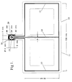
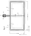
- A planar antenna, characterised in that said antenna comprises a rectangular conductive element formed from two square elements, the square elements being defined within the rectangle by a centrally located return conductor, each said square element being connected at one end to a connector element, and at the other end to said return conductor, wherein the dimensions of the square elements are chosen so as to maximise gain for selected radio frequencies.
- An antenna according to claim 1, wherein the conductive elements are formed on a substrate.
- An antenna according to claim 2, wherein the substrate is a flexible film.
- An antenna according to claim 2 or claim 3, wherein the substrate is transparent.
- An antenna according to claim 1, wherein both square elements are electrically connected to the same connector element, and the return conductor is connected to an electrically separate connector element.
- An antenna according to claim 1, wherein said antenna further includes one or more additional square elements disposed within said square elements, each additional square element being connected to the respective square element at one end and being defined by the return conductor on one side.
- An antenna according to claim 6, wherein the conductive elements are formed on a substrate.
- An antenna according to claim 7, wherein the substrate is a flexible film.
- An antenna according to claim 7 or claim 8, wherein the substrate is transparent.
- An antenna according to claim 6, wherein both square elements are electrically connected to the same connector element, and the return conductor is connected to an electrically separate connector element.
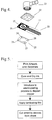
- A method for providing conductive elements on a substrate, characterised in that the method includes the steps of:printing a conductor pattern onto a substrate, using conductive ink; andelectrodepositing further conductive material onto the printed conductor pattern, using the pattern formed from conductive ink as an electrode in an electroplating process.
- A method according to claim 11, wherein the substrate is flexible.
- A method according to claim 11 or claim 12, wherein the substrate is transparent.
- A method according to claim 11, wherein the conductor pattern is screen printed onto said substrate.
- A method according to claim 14, wherein a plurality of conductor patterns are printed onto said substrate, and after electrodeposition a protective film is applied to the conductor pattern.
- A method according to claim 15, wherein after the film is applied the substrate is cut to form a plurality of devices.
- A method according to claim 15 or claim 16, wherein the film is adhesive on both sides.
- A device including conductive elements formed by the method of claim 11.
Applications Claiming Priority (5)
| Application Number | Priority Date | Filing Date | Title |
|---|---|---|---|
| AUPO929897 | 1997-09-19 | ||
| AUPO9298/97 | 1997-09-19 | ||
| AUPO9298A AUPO929897A0 (en) | 1997-09-19 | 1997-09-19 | Transparent mobile communication antenna |
| US09/098,771 US6252550B1 (en) | 1998-06-17 | 1998-06-17 | Planar antenna device |
| US98771 | 1998-06-17 |
Publications (3)
| Publication Number | Publication Date |
|---|---|
| EP0903805A2 true EP0903805A2 (en) | 1999-03-24 |
| EP0903805A3 EP0903805A3 (en) | 1999-06-09 |
| EP0903805B1 EP0903805B1 (en) | 2003-08-06 |
Family
ID=25645616
Family Applications (1)
| Application Number | Title | Priority Date | Filing Date |
|---|---|---|---|
| EP98116584A Expired - Lifetime EP0903805B1 (en) | 1997-09-19 | 1998-09-02 | Planar antenna device |
Country Status (3)
| Country | Link |
|---|---|
| EP (1) | EP0903805B1 (en) |
| AT (1) | ATE246847T1 (en) |
| DE (1) | DE69816922T2 (en) |
Cited By (16)
| Publication number | Priority date | Publication date | Assignee | Title |
|---|---|---|---|---|
| GB2355116A (en) * | 1999-10-08 | 2001-04-11 | Nokia Mobile Phones Ltd | Flexible planar mobile 'phone antenna |
| EP1266426A1 (en) * | 2000-03-13 | 2002-12-18 | RCD Technology, Inc. | Method for forming radio frequency antenna using conductive inks |
| EP1388186A1 (en) * | 2001-03-26 | 2004-02-11 | Daniel Luch | Electrically conductive patterns, antennas and methods of manufacture |
| EP1555715A1 (en) * | 2004-01-13 | 2005-07-20 | Kabushiki Kaisha Toshiba | Antenna device and mobile communication terminal equipped with antenna device |
| WO2007037999A1 (en) * | 2005-09-26 | 2007-04-05 | Motorola Inc. | Multi-band antenna |
| US7268740B2 (en) | 2000-03-13 | 2007-09-11 | Rcd Technology Inc. | Method for forming radio frequency antenna |
| US7298331B2 (en) | 2000-03-13 | 2007-11-20 | Rcd Technology, Inc. | Method for forming radio frequency antenna |
| EP1901392A1 (en) * | 2006-09-14 | 2008-03-19 | Nippon Sheet Glass Company Limited | On-vehicle film antenna apparatus |
| US7377447B2 (en) | 2005-12-05 | 2008-05-27 | Rcd Technology, Inc. | Tuned radio frequency identification (RFID) circuit used as a security device for wristbands and package security |
| WO2008066811A2 (en) * | 2006-11-30 | 2008-06-05 | Corning Cable Systems Llc | Locatable fibre optic cable comprising antenna of conductive ink |
| US7388542B2 (en) | 2005-11-10 | 2008-06-17 | Rcd Technology, Inc. | Method for an element using two resist layers |
| US7456506B2 (en) | 2005-03-14 | 2008-11-25 | Rcd Technology Inc. | Radio frequency identification (RFID) tag lamination process using liner |
| US7456752B2 (en) | 2003-05-06 | 2008-11-25 | Rcd Technology, Inc. | Radio frequency identification sensor for fluid level |
| US7674649B2 (en) | 2005-03-14 | 2010-03-09 | Rcd Technology Inc. | Radio frequency identification (RFID) tag lamination process using liner |
| WO2015110658A1 (en) * | 2014-01-27 | 2015-07-30 | Hirschmann Car Communication Gmbh | Vehicle antennas having a flexible substrate as the antenna support |
| WO2020259981A1 (en) | 2019-06-25 | 2020-12-30 | Saint-Gobain Glass France | Electrical connection element for glazing |
Citations (12)
| Publication number | Priority date | Publication date | Assignee | Title |
|---|---|---|---|---|
| WO1983002538A1 (en) * | 1982-01-04 | 1983-07-21 | Gen Electric | Electroplated augmentative replacement processed conductors and manufacture thereof |
| US4470883A (en) * | 1983-05-02 | 1984-09-11 | General Electric Company | Additive printed circuit process |
| EP0195612A2 (en) * | 1985-03-16 | 1986-09-24 | Marconi Electronic Devices Limited | Printed circuit arrangement |
| US4737797A (en) * | 1986-06-26 | 1988-04-12 | Motorola, Inc. | Microstrip balun-antenna apparatus |
| US4860019A (en) * | 1987-11-16 | 1989-08-22 | Shanghai Dong Hai Military Technology Engineering Co. | Planar TV receiving antenna with broad band |
| WO1991009511A2 (en) * | 1989-12-19 | 1991-06-27 | Technology Applications Company Limited | Electrical conductors of conductive resin |
| EP0443097A1 (en) * | 1990-02-23 | 1991-08-28 | Carl Baasel Lasertechnik GmbH | Three dimensional plating or etching process and masks therefor |
| EP0516303A1 (en) * | 1991-05-14 | 1992-12-02 | Sony Corporation | Planar antenna |
| CH684540A5 (en) * | 1991-12-24 | 1994-10-14 | Shih Chang Hsu | Process for producing a multilayer metal pattern |
| US5363114A (en) * | 1990-01-29 | 1994-11-08 | Shoemaker Kevin O | Planar serpentine antennas |
| EP0762539A1 (en) * | 1995-08-17 | 1997-03-12 | Murata Manufacturing Co., Ltd. | Chip antenna |
| EP0786824A1 (en) * | 1996-01-27 | 1997-07-30 | Akitoshi Imamura | A microloop antenna |
-
1998
- 1998-09-02 EP EP98116584A patent/EP0903805B1/en not_active Expired - Lifetime
- 1998-09-02 AT AT98116584T patent/ATE246847T1/en not_active IP Right Cessation
- 1998-09-02 DE DE69816922T patent/DE69816922T2/en not_active Expired - Fee Related
Patent Citations (12)
| Publication number | Priority date | Publication date | Assignee | Title |
|---|---|---|---|---|
| WO1983002538A1 (en) * | 1982-01-04 | 1983-07-21 | Gen Electric | Electroplated augmentative replacement processed conductors and manufacture thereof |
| US4470883A (en) * | 1983-05-02 | 1984-09-11 | General Electric Company | Additive printed circuit process |
| EP0195612A2 (en) * | 1985-03-16 | 1986-09-24 | Marconi Electronic Devices Limited | Printed circuit arrangement |
| US4737797A (en) * | 1986-06-26 | 1988-04-12 | Motorola, Inc. | Microstrip balun-antenna apparatus |
| US4860019A (en) * | 1987-11-16 | 1989-08-22 | Shanghai Dong Hai Military Technology Engineering Co. | Planar TV receiving antenna with broad band |
| WO1991009511A2 (en) * | 1989-12-19 | 1991-06-27 | Technology Applications Company Limited | Electrical conductors of conductive resin |
| US5363114A (en) * | 1990-01-29 | 1994-11-08 | Shoemaker Kevin O | Planar serpentine antennas |
| EP0443097A1 (en) * | 1990-02-23 | 1991-08-28 | Carl Baasel Lasertechnik GmbH | Three dimensional plating or etching process and masks therefor |
| EP0516303A1 (en) * | 1991-05-14 | 1992-12-02 | Sony Corporation | Planar antenna |
| CH684540A5 (en) * | 1991-12-24 | 1994-10-14 | Shih Chang Hsu | Process for producing a multilayer metal pattern |
| EP0762539A1 (en) * | 1995-08-17 | 1997-03-12 | Murata Manufacturing Co., Ltd. | Chip antenna |
| EP0786824A1 (en) * | 1996-01-27 | 1997-07-30 | Akitoshi Imamura | A microloop antenna |
Cited By (28)
| Publication number | Priority date | Publication date | Assignee | Title |
|---|---|---|---|---|
| US6784844B1 (en) | 1999-10-08 | 2004-08-31 | Nokia Mobile Phone Limited | Antenna assembly and method of construction |
| GB2355116A (en) * | 1999-10-08 | 2001-04-11 | Nokia Mobile Phones Ltd | Flexible planar mobile 'phone antenna |
| GB2355116B (en) * | 1999-10-08 | 2003-10-08 | Nokia Mobile Phones Ltd | An antenna assembly and method of construction |
| US6933892B2 (en) | 2000-03-13 | 2005-08-23 | Rcd Technology Corp. | Method for forming radio frequency antenna |
| US7268740B2 (en) | 2000-03-13 | 2007-09-11 | Rcd Technology Inc. | Method for forming radio frequency antenna |
| EP1266426A4 (en) * | 2000-03-13 | 2004-12-08 | Rcd Technology Inc | Method for forming radio frequency antenna using conductive inks |
| US7515116B2 (en) | 2000-03-13 | 2009-04-07 | Rcd Technology, Inc. | Method for forming radio frequency antenna |
| US7639184B2 (en) | 2000-03-13 | 2009-12-29 | Rcd Technology Inc. | Method for forming radio frequency antenna |
| EP1266426A1 (en) * | 2000-03-13 | 2002-12-18 | RCD Technology, Inc. | Method for forming radio frequency antenna using conductive inks |
| US7298331B2 (en) | 2000-03-13 | 2007-11-20 | Rcd Technology, Inc. | Method for forming radio frequency antenna |
| EP1388186A4 (en) * | 2001-03-26 | 2005-08-17 | Daniel Luch | Electrically conductive patterns, antennas and methods of manufacture |
| EP1388186A1 (en) * | 2001-03-26 | 2004-02-11 | Daniel Luch | Electrically conductive patterns, antennas and methods of manufacture |
| US7456752B2 (en) | 2003-05-06 | 2008-11-25 | Rcd Technology, Inc. | Radio frequency identification sensor for fluid level |
| US7358906B2 (en) | 2004-01-13 | 2008-04-15 | Kabushiki Kaisha Toshiba | Antenna device and mobile communication terminal equipped with antenna device |
| EP1555715A1 (en) * | 2004-01-13 | 2005-07-20 | Kabushiki Kaisha Toshiba | Antenna device and mobile communication terminal equipped with antenna device |
| US7674649B2 (en) | 2005-03-14 | 2010-03-09 | Rcd Technology Inc. | Radio frequency identification (RFID) tag lamination process using liner |
| US7456506B2 (en) | 2005-03-14 | 2008-11-25 | Rcd Technology Inc. | Radio frequency identification (RFID) tag lamination process using liner |
| WO2007037999A1 (en) * | 2005-09-26 | 2007-04-05 | Motorola Inc. | Multi-band antenna |
| US7388542B2 (en) | 2005-11-10 | 2008-06-17 | Rcd Technology, Inc. | Method for an element using two resist layers |
| US7377447B2 (en) | 2005-12-05 | 2008-05-27 | Rcd Technology, Inc. | Tuned radio frequency identification (RFID) circuit used as a security device for wristbands and package security |
| EP1901392A1 (en) * | 2006-09-14 | 2008-03-19 | Nippon Sheet Glass Company Limited | On-vehicle film antenna apparatus |
| WO2008066811A3 (en) * | 2006-11-30 | 2008-07-24 | Corning Cable Sys Llc | Locatable fibre optic cable comprising antenna of conductive ink |
| US7526163B2 (en) | 2006-11-30 | 2009-04-28 | Corning Cable Systems Llc | Locatable cables and cable components therefor |
| WO2008066811A2 (en) * | 2006-11-30 | 2008-06-05 | Corning Cable Systems Llc | Locatable fibre optic cable comprising antenna of conductive ink |
| WO2015110658A1 (en) * | 2014-01-27 | 2015-07-30 | Hirschmann Car Communication Gmbh | Vehicle antennas having a flexible substrate as the antenna support |
| DE102015201379B4 (en) * | 2014-01-27 | 2021-02-11 | Hirschmann Car Communication Gmbh | Vehicle antennas with a flexible substrate as antenna carrier |
| WO2020259981A1 (en) | 2019-06-25 | 2020-12-30 | Saint-Gobain Glass France | Electrical connection element for glazing |
| DE202020005572U1 (en) | 2019-06-25 | 2021-11-03 | Saint-Gobain Glass France | Electrical connection element for glazing |
Also Published As
| Publication number | Publication date |
|---|---|
| EP0903805A3 (en) | 1999-06-09 |
| DE69816922D1 (en) | 2003-09-11 |
| DE69816922T2 (en) | 2004-07-15 |
| EP0903805B1 (en) | 2003-08-06 |
| ATE246847T1 (en) | 2003-08-15 |
Similar Documents
| Publication | Publication Date | Title |
|---|---|---|
| EP0903805B1 (en) | Planar antenna device | |
| US6252550B1 (en) | Planar antenna device | |
| US5041838A (en) | Cellular telephone antenna | |
| US6556812B1 (en) | Antenna coupler and arrangement for coupling a radio telecommunication device to external apparatuses | |
| US6157344A (en) | Flat panel antenna | |
| CN100466377C (en) | Multi-band planar antenna | |
| JP2003078320A (en) | Antenna unit and computer terminal comprising the same | |
| JP2003500956A (en) | Radiating housing | |
| US20110309985A1 (en) | Wideband printed circuit board-printed antenna for radio frequency front end circuit | |
| WO2004027681A3 (en) | Rfid tag wide bandwidth logarithmic spiral antenna method and system | |
| US6407706B2 (en) | Planar antenna device | |
| US6421018B1 (en) | Bowtie inductive coupler | |
| PL204755B1 (en) | Antenna window with high frequency component | |
| US20080261667A1 (en) | Mobile terminal having an improved internal antenna | |
| US8433269B2 (en) | Compact satellite antenna | |
| EP0853827A1 (en) | Vehicle antenna | |
| US8704714B2 (en) | Surface mount module embedded antenna | |
| CN1183174A (en) | Antenna and assembly | |
| JPH06152237A (en) | Patch antenna system | |
| AU783548B2 (en) | Planar antenna device | |
| JP7383729B2 (en) | vehicle pane | |
| KR102239231B1 (en) | Combo antenna module and manufacturing method thereof | |
| CN214124114U (en) | Vehicle-mounted antenna | |
| CN216793985U (en) | Antenna device, glass, antenna system and vehicle | |
| JPH0766627A (en) | Planar patch antenna system |
Legal Events
| Date | Code | Title | Description |
|---|---|---|---|
| PUAI | Public reference made under article 153(3) epc to a published international application that has entered the european phase |
Free format text: ORIGINAL CODE: 0009012 |
|
| AK | Designated contracting states |
Kind code of ref document: A2 Designated state(s): AT BE CH CY DE DK ES FI FR GB GR IE IT LI LU MC NL PT SE |
|
| AX | Request for extension of the european patent |
Free format text: AL;LT;LV;MK;RO;SI |
|
| PUAL | Search report despatched |
Free format text: ORIGINAL CODE: 0009013 |
|
| AK | Designated contracting states |
Kind code of ref document: A3 Designated state(s): AT BE CH CY DE DK ES FI FR GB GR IE IT LI LU MC NL PT SE |
|
| AX | Request for extension of the european patent |
Free format text: AL;LT;LV;MK;RO;SI |
|
| RIC1 | Information provided on ipc code assigned before grant |
Free format text: 6H 01Q 1/38 A, 6H 01Q 1/12 B, 6H 05K 1/09 B |
|
| AKX | Designation fees paid | ||
| REG | Reference to a national code |
Ref country code: DE Ref legal event code: 8566 |
|
| 17P | Request for examination filed |
Effective date: 19991209 |
|
| RBV | Designated contracting states (corrected) |
Designated state(s): AT BE CH CY DE DK ES FI FR GB GR IE IT LI LU MC NL PT SE |
|
| RAX | Requested extension states of the european patent have changed |
Free format text: AL PAYMENT 19991209;LT PAYMENT 19991209;LV PAYMENT 19991209;MK PAYMENT 19991209;RO PAYMENT 19991209;SI PAYMENT 19991209 |
|
| 17Q | First examination report despatched |
Effective date: 20000620 |
|
| GRAH | Despatch of communication of intention to grant a patent |
Free format text: ORIGINAL CODE: EPIDOS IGRA |
|
| RTI1 | Title (correction) |
Free format text: PLANAR ANTENNA DEVICE |
|
| GRAH | Despatch of communication of intention to grant a patent |
Free format text: ORIGINAL CODE: EPIDOS IGRA |
|
| GRAA | (expected) grant |
Free format text: ORIGINAL CODE: 0009210 |
|
| AK | Designated contracting states |
Designated state(s): AT BE CH CY DE DK ES FI FR GB GR IE IT LI LU MC NL PT SE |
|
| AX | Request for extension of the european patent |
Extension state: AL LT LV MK RO SI |
|
| PG25 | Lapsed in a contracting state [announced via postgrant information from national office to epo] |
Ref country code: NL Free format text: LAPSE BECAUSE OF FAILURE TO SUBMIT A TRANSLATION OF THE DESCRIPTION OR TO PAY THE FEE WITHIN THE PRESCRIBED TIME-LIMIT Effective date: 20030806 Ref country code: LI Free format text: LAPSE BECAUSE OF FAILURE TO SUBMIT A TRANSLATION OF THE DESCRIPTION OR TO PAY THE FEE WITHIN THE PRESCRIBED TIME-LIMIT Effective date: 20030806 Ref country code: IT Free format text: LAPSE BECAUSE OF FAILURE TO SUBMIT A TRANSLATION OF THE DESCRIPTION OR TO PAY THE FEE WITHIN THE PRESCRIBED TIME-LIMIT;WARNING: LAPSES OF ITALIAN PATENTS WITH EFFECTIVE DATE BEFORE 2007 MAY HAVE OCCURRED AT ANY TIME BEFORE 2007. THE CORRECT EFFECTIVE DATE MAY BE DIFFERENT FROM THE ONE RECORDED. Effective date: 20030806 Ref country code: CH Free format text: LAPSE BECAUSE OF FAILURE TO SUBMIT A TRANSLATION OF THE DESCRIPTION OR TO PAY THE FEE WITHIN THE PRESCRIBED TIME-LIMIT Effective date: 20030806 Ref country code: BE Free format text: LAPSE BECAUSE OF FAILURE TO SUBMIT A TRANSLATION OF THE DESCRIPTION OR TO PAY THE FEE WITHIN THE PRESCRIBED TIME-LIMIT Effective date: 20030806 Ref country code: AT Free format text: LAPSE BECAUSE OF FAILURE TO SUBMIT A TRANSLATION OF THE DESCRIPTION OR TO PAY THE FEE WITHIN THE PRESCRIBED TIME-LIMIT Effective date: 20030806 |
|
| REG | Reference to a national code |
Ref country code: GB Ref legal event code: FG4D |
|
| REG | Reference to a national code |
Ref country code: CH Ref legal event code: EP |
|
| PG25 | Lapsed in a contracting state [announced via postgrant information from national office to epo] |
Ref country code: LU Free format text: LAPSE BECAUSE OF NON-PAYMENT OF DUE FEES Effective date: 20030902 Ref country code: IE Free format text: LAPSE BECAUSE OF NON-PAYMENT OF DUE FEES Effective date: 20030902 Ref country code: CY Free format text: LAPSE BECAUSE OF FAILURE TO SUBMIT A TRANSLATION OF THE DESCRIPTION OR TO PAY THE FEE WITHIN THE PRESCRIBED TIME-LIMIT Effective date: 20030902 |
|
| REG | Reference to a national code |
Ref country code: IE Ref legal event code: FG4D |
|
| REF | Corresponds to: |
Ref document number: 69816922 Country of ref document: DE Date of ref document: 20030911 Kind code of ref document: P |
|
| PG25 | Lapsed in a contracting state [announced via postgrant information from national office to epo] |
Ref country code: MC Free format text: LAPSE BECAUSE OF NON-PAYMENT OF DUE FEES Effective date: 20030930 |
|
| REG | Reference to a national code |
Ref country code: SE Ref legal event code: TRGR |
|
| PG25 | Lapsed in a contracting state [announced via postgrant information from national office to epo] |
Ref country code: GR Free format text: LAPSE BECAUSE OF FAILURE TO SUBMIT A TRANSLATION OF THE DESCRIPTION OR TO PAY THE FEE WITHIN THE PRESCRIBED TIME-LIMIT Effective date: 20031106 Ref country code: DK Free format text: LAPSE BECAUSE OF FAILURE TO SUBMIT A TRANSLATION OF THE DESCRIPTION OR TO PAY THE FEE WITHIN THE PRESCRIBED TIME-LIMIT Effective date: 20031106 |
|
| PG25 | Lapsed in a contracting state [announced via postgrant information from national office to epo] |
Ref country code: ES Free format text: LAPSE BECAUSE OF FAILURE TO SUBMIT A TRANSLATION OF THE DESCRIPTION OR TO PAY THE FEE WITHIN THE PRESCRIBED TIME-LIMIT Effective date: 20031117 |
|
| NLV1 | Nl: lapsed or annulled due to failure to fulfill the requirements of art. 29p and 29m of the patents act | ||
| PG25 | Lapsed in a contracting state [announced via postgrant information from national office to epo] |
Ref country code: PT Free format text: LAPSE BECAUSE OF FAILURE TO SUBMIT A TRANSLATION OF THE DESCRIPTION OR TO PAY THE FEE WITHIN THE PRESCRIBED TIME-LIMIT Effective date: 20040106 |
|
| LTIE | Lt: invalidation of european patent or patent extension |
Effective date: 20030806 |
|
| REG | Reference to a national code |
Ref country code: CH Ref legal event code: PL |
|
| ET | Fr: translation filed | ||
| PLBE | No opposition filed within time limit |
Free format text: ORIGINAL CODE: 0009261 |
|
| STAA | Information on the status of an ep patent application or granted ep patent |
Free format text: STATUS: NO OPPOSITION FILED WITHIN TIME LIMIT |
|
| REG | Reference to a national code |
Ref country code: IE Ref legal event code: MM4A |
|
| 26N | No opposition filed |
Effective date: 20040507 |
|
| PGFP | Annual fee paid to national office [announced via postgrant information from national office to epo] |
Ref country code: FR Payment date: 20050920 Year of fee payment: 8 |
|
| PGFP | Annual fee paid to national office [announced via postgrant information from national office to epo] |
Ref country code: SE Payment date: 20050923 Year of fee payment: 8 Ref country code: FI Payment date: 20050923 Year of fee payment: 8 |
|
| PG25 | Lapsed in a contracting state [announced via postgrant information from national office to epo] |
Ref country code: FI Free format text: LAPSE BECAUSE OF NON-PAYMENT OF DUE FEES Effective date: 20060902 |
|
| PG25 | Lapsed in a contracting state [announced via postgrant information from national office to epo] |
Ref country code: SE Free format text: LAPSE BECAUSE OF NON-PAYMENT OF DUE FEES Effective date: 20060903 |
|
| PGFP | Annual fee paid to national office [announced via postgrant information from national office to epo] |
Ref country code: DE Payment date: 20070301 Year of fee payment: 9 |
|
| PGFP | Annual fee paid to national office [announced via postgrant information from national office to epo] |
Ref country code: GB Payment date: 20070302 Year of fee payment: 9 |
|
| EUG | Se: european patent has lapsed | ||
| REG | Reference to a national code |
Ref country code: FR Ref legal event code: ST Effective date: 20070531 |
|
| PG25 | Lapsed in a contracting state [announced via postgrant information from national office to epo] |
Ref country code: FR Free format text: LAPSE BECAUSE OF NON-PAYMENT OF DUE FEES Effective date: 20061002 |
|
| GBPC | Gb: european patent ceased through non-payment of renewal fee |
Effective date: 20070902 |
|
| PG25 | Lapsed in a contracting state [announced via postgrant information from national office to epo] |
Ref country code: DE Free format text: LAPSE BECAUSE OF NON-PAYMENT OF DUE FEES Effective date: 20080401 |
|
| PG25 | Lapsed in a contracting state [announced via postgrant information from national office to epo] |
Ref country code: GB Free format text: LAPSE BECAUSE OF NON-PAYMENT OF DUE FEES Effective date: 20070902 |