EP0905751A2 - Method for minimizing lateral and vertical dopant diffusion in gate structures - Google Patents
Method for minimizing lateral and vertical dopant diffusion in gate structures Download PDFInfo
- Publication number
- EP0905751A2 EP0905751A2 EP98307025A EP98307025A EP0905751A2 EP 0905751 A2 EP0905751 A2 EP 0905751A2 EP 98307025 A EP98307025 A EP 98307025A EP 98307025 A EP98307025 A EP 98307025A EP 0905751 A2 EP0905751 A2 EP 0905751A2
- Authority
- EP
- European Patent Office
- Prior art keywords
- layer
- silicon
- oxide layer
- gate
- over
- Prior art date
- Legal status (The legal status is an assumption and is not a legal conclusion. Google has not performed a legal analysis and makes no representation as to the accuracy of the status listed.)
- Granted
Links
- 239000002019 doping agent Substances 0.000 title claims abstract description 61
- 238000000034 method Methods 0.000 title claims abstract description 58
- 238000009792 diffusion process Methods 0.000 title claims description 23
- XUIMIQQOPSSXEZ-UHFFFAOYSA-N Silicon Chemical group [Si] XUIMIQQOPSSXEZ-UHFFFAOYSA-N 0.000 claims abstract description 215
- 229910052710 silicon Inorganic materials 0.000 claims abstract description 162
- 239000010703 silicon Substances 0.000 claims abstract description 162
- 230000004888 barrier function Effects 0.000 claims abstract description 86
- 229910021332 silicide Inorganic materials 0.000 claims abstract description 59
- FVBUAEGBCNSCDD-UHFFFAOYSA-N silicide(4-) Chemical compound [Si-4] FVBUAEGBCNSCDD-UHFFFAOYSA-N 0.000 claims abstract description 56
- 239000000758 substrate Substances 0.000 claims abstract description 41
- 150000004767 nitrides Chemical class 0.000 claims abstract description 18
- IJGRMHOSHXDMSA-UHFFFAOYSA-N Atomic nitrogen Chemical compound N#N IJGRMHOSHXDMSA-UHFFFAOYSA-N 0.000 claims abstract description 14
- 238000005530 etching Methods 0.000 claims abstract description 9
- 238000000151 deposition Methods 0.000 claims abstract description 8
- 229910052757 nitrogen Inorganic materials 0.000 claims abstract description 7
- 229910021420 polycrystalline silicon Inorganic materials 0.000 claims description 12
- 230000009977 dual effect Effects 0.000 claims description 11
- 229920005591 polysilicon Polymers 0.000 claims description 6
- ZOXJGFHDIHLPTG-UHFFFAOYSA-N Boron Chemical compound [B] ZOXJGFHDIHLPTG-UHFFFAOYSA-N 0.000 claims description 5
- 229910052785 arsenic Inorganic materials 0.000 claims description 5
- RQNWIZPPADIBDY-UHFFFAOYSA-N arsenic atom Chemical compound [As] RQNWIZPPADIBDY-UHFFFAOYSA-N 0.000 claims description 5
- 229910052796 boron Inorganic materials 0.000 claims description 5
- BHEPBYXIRTUNPN-UHFFFAOYSA-N hydridophosphorus(.) (triplet) Chemical compound [PH] BHEPBYXIRTUNPN-UHFFFAOYSA-N 0.000 claims description 5
- 238000005229 chemical vapour deposition Methods 0.000 claims description 4
- 238000000137 annealing Methods 0.000 description 13
- 230000015572 biosynthetic process Effects 0.000 description 9
- 238000004519 manufacturing process Methods 0.000 description 8
- VYPSYNLAJGMNEJ-UHFFFAOYSA-N Silicium dioxide Chemical compound O=[Si]=O VYPSYNLAJGMNEJ-UHFFFAOYSA-N 0.000 description 4
- 239000000463 material Substances 0.000 description 4
- QGZKDVFQNNGYKY-UHFFFAOYSA-N Ammonia Chemical compound N QGZKDVFQNNGYKY-UHFFFAOYSA-N 0.000 description 3
- 238000011109 contamination Methods 0.000 description 3
- 238000010586 diagram Methods 0.000 description 3
- 239000004065 semiconductor Substances 0.000 description 3
- 229910021341 titanium silicide Inorganic materials 0.000 description 3
- WQJQOUPTWCFRMM-UHFFFAOYSA-N tungsten disilicide Chemical compound [Si]#[W]#[Si] WQJQOUPTWCFRMM-UHFFFAOYSA-N 0.000 description 3
- 229910021342 tungsten silicide Inorganic materials 0.000 description 3
- 229910004205 SiNX Inorganic materials 0.000 description 2
- 238000001459 lithography Methods 0.000 description 2
- 238000004518 low pressure chemical vapour deposition Methods 0.000 description 2
- 230000014759 maintenance of location Effects 0.000 description 2
- 239000012466 permeate Substances 0.000 description 2
- 238000000623 plasma-assisted chemical vapour deposition Methods 0.000 description 2
- 239000000047 product Substances 0.000 description 2
- 239000000377 silicon dioxide Substances 0.000 description 2
- JBRZTFJDHDCESZ-UHFFFAOYSA-N AsGa Chemical compound [As]#[Ga] JBRZTFJDHDCESZ-UHFFFAOYSA-N 0.000 description 1
- 229910019044 CoSix Inorganic materials 0.000 description 1
- 208000032750 Device leakage Diseases 0.000 description 1
- 229910001218 Gallium arsenide Inorganic materials 0.000 description 1
- 229910052581 Si3N4 Inorganic materials 0.000 description 1
- 229910008486 TiSix Inorganic materials 0.000 description 1
- 229910021529 ammonia Inorganic materials 0.000 description 1
- QVGXLLKOCUKJST-UHFFFAOYSA-N atomic oxygen Chemical compound [O] QVGXLLKOCUKJST-UHFFFAOYSA-N 0.000 description 1
- YXTPWUNVHCYOSP-UHFFFAOYSA-N bis($l^{2}-silanylidene)molybdenum Chemical compound [Si]=[Mo]=[Si] YXTPWUNVHCYOSP-UHFFFAOYSA-N 0.000 description 1
- 230000001413 cellular effect Effects 0.000 description 1
- 239000010941 cobalt Substances 0.000 description 1
- 229910017052 cobalt Inorganic materials 0.000 description 1
- GUTLYIVDDKVIGB-UHFFFAOYSA-N cobalt atom Chemical compound [Co] GUTLYIVDDKVIGB-UHFFFAOYSA-N 0.000 description 1
- 230000001419 dependent effect Effects 0.000 description 1
- 239000003989 dielectric material Substances 0.000 description 1
- 238000001312 dry etching Methods 0.000 description 1
- 239000012467 final product Substances 0.000 description 1
- 239000007789 gas Substances 0.000 description 1
- 229910052732 germanium Inorganic materials 0.000 description 1
- GNPVGFCGXDBREM-UHFFFAOYSA-N germanium atom Chemical compound [Ge] GNPVGFCGXDBREM-UHFFFAOYSA-N 0.000 description 1
- 238000002513 implantation Methods 0.000 description 1
- 238000011065 in-situ storage Methods 0.000 description 1
- 239000012212 insulator Substances 0.000 description 1
- 239000011159 matrix material Substances 0.000 description 1
- 238000001465 metallisation Methods 0.000 description 1
- 229910021344 molybdenum silicide Inorganic materials 0.000 description 1
- 229910000069 nitrogen hydride Inorganic materials 0.000 description 1
- 230000003647 oxidation Effects 0.000 description 1
- 238000007254 oxidation reaction Methods 0.000 description 1
- 239000001301 oxygen Substances 0.000 description 1
- 229910052760 oxygen Inorganic materials 0.000 description 1
- 235000012239 silicon dioxide Nutrition 0.000 description 1
- HQVNEWCFYHHQES-UHFFFAOYSA-N silicon nitride Chemical compound N12[Si]34N5[Si]62N3[Si]51N64 HQVNEWCFYHHQES-UHFFFAOYSA-N 0.000 description 1
- 125000006850 spacer group Chemical group 0.000 description 1
- 230000001360 synchronised effect Effects 0.000 description 1
- 229910052715 tantalum Inorganic materials 0.000 description 1
- GUVRBAGPIYLISA-UHFFFAOYSA-N tantalum atom Chemical compound [Ta] GUVRBAGPIYLISA-UHFFFAOYSA-N 0.000 description 1
Images


Classifications
-
- H—ELECTRICITY
- H01—ELECTRIC ELEMENTS
- H01L—SEMICONDUCTOR DEVICES NOT COVERED BY CLASS H10
- H01L21/00—Processes or apparatus adapted for the manufacture or treatment of semiconductor or solid state devices or of parts thereof
- H01L21/02—Manufacture or treatment of semiconductor devices or of parts thereof
- H01L21/04—Manufacture or treatment of semiconductor devices or of parts thereof the devices having at least one potential-jump barrier or surface barrier, e.g. PN junction, depletion layer or carrier concentration layer
- H01L21/18—Manufacture or treatment of semiconductor devices or of parts thereof the devices having at least one potential-jump barrier or surface barrier, e.g. PN junction, depletion layer or carrier concentration layer the devices having semiconductor bodies comprising elements of Group IV of the Periodic System or AIIIBV compounds with or without impurities, e.g. doping materials
-
- H—ELECTRICITY
- H01—ELECTRIC ELEMENTS
- H01L—SEMICONDUCTOR DEVICES NOT COVERED BY CLASS H10
- H01L21/00—Processes or apparatus adapted for the manufacture or treatment of semiconductor or solid state devices or of parts thereof
- H01L21/70—Manufacture or treatment of devices consisting of a plurality of solid state components formed in or on a common substrate or of parts thereof; Manufacture of integrated circuit devices or of parts thereof
- H01L21/77—Manufacture or treatment of devices consisting of a plurality of solid state components or integrated circuits formed in, or on, a common substrate
- H01L21/78—Manufacture or treatment of devices consisting of a plurality of solid state components or integrated circuits formed in, or on, a common substrate with subsequent division of the substrate into plural individual devices
- H01L21/82—Manufacture or treatment of devices consisting of a plurality of solid state components or integrated circuits formed in, or on, a common substrate with subsequent division of the substrate into plural individual devices to produce devices, e.g. integrated circuits, each consisting of a plurality of components
- H01L21/822—Manufacture or treatment of devices consisting of a plurality of solid state components or integrated circuits formed in, or on, a common substrate with subsequent division of the substrate into plural individual devices to produce devices, e.g. integrated circuits, each consisting of a plurality of components the substrate being a semiconductor, using silicon technology
- H01L21/8232—Field-effect technology
- H01L21/8234—MIS technology, i.e. integration processes of field effect transistors of the conductor-insulator-semiconductor type
- H01L21/8238—Complementary field-effect transistors, e.g. CMOS
-
- H—ELECTRICITY
- H01—ELECTRIC ELEMENTS
- H01L—SEMICONDUCTOR DEVICES NOT COVERED BY CLASS H10
- H01L21/00—Processes or apparatus adapted for the manufacture or treatment of semiconductor or solid state devices or of parts thereof
- H01L21/02—Manufacture or treatment of semiconductor devices or of parts thereof
- H01L21/04—Manufacture or treatment of semiconductor devices or of parts thereof the devices having at least one potential-jump barrier or surface barrier, e.g. PN junction, depletion layer or carrier concentration layer
- H01L21/18—Manufacture or treatment of semiconductor devices or of parts thereof the devices having at least one potential-jump barrier or surface barrier, e.g. PN junction, depletion layer or carrier concentration layer the devices having semiconductor bodies comprising elements of Group IV of the Periodic System or AIIIBV compounds with or without impurities, e.g. doping materials
- H01L21/28—Manufacture of electrodes on semiconductor bodies using processes or apparatus not provided for in groups H01L21/20 - H01L21/268
- H01L21/28008—Making conductor-insulator-semiconductor electrodes
- H01L21/28017—Making conductor-insulator-semiconductor electrodes the insulator being formed after the semiconductor body, the semiconductor being silicon
- H01L21/28026—Making conductor-insulator-semiconductor electrodes the insulator being formed after the semiconductor body, the semiconductor being silicon characterised by the conductor
- H01L21/28035—Making conductor-insulator-semiconductor electrodes the insulator being formed after the semiconductor body, the semiconductor being silicon characterised by the conductor the final conductor layer next to the insulator being silicon, e.g. polysilicon, with or without impurities
- H01L21/28044—Making conductor-insulator-semiconductor electrodes the insulator being formed after the semiconductor body, the semiconductor being silicon characterised by the conductor the final conductor layer next to the insulator being silicon, e.g. polysilicon, with or without impurities the conductor comprising at least another non-silicon conductive layer
- H01L21/28061—Making conductor-insulator-semiconductor electrodes the insulator being formed after the semiconductor body, the semiconductor being silicon characterised by the conductor the final conductor layer next to the insulator being silicon, e.g. polysilicon, with or without impurities the conductor comprising at least another non-silicon conductive layer the conductor comprising a metal or metal silicide formed by deposition, e.g. sputter deposition, i.e. without a silicidation reaction
-
- H—ELECTRICITY
- H01—ELECTRIC ELEMENTS
- H01L—SEMICONDUCTOR DEVICES NOT COVERED BY CLASS H10
- H01L29/00—Semiconductor devices adapted for rectifying, amplifying, oscillating or switching, or capacitors or resistors with at least one potential-jump barrier or surface barrier, e.g. PN junction depletion layer or carrier concentration layer; Details of semiconductor bodies or of electrodes thereof ; Multistep manufacturing processes therefor
- H01L29/40—Electrodes ; Multistep manufacturing processes therefor
- H01L29/43—Electrodes ; Multistep manufacturing processes therefor characterised by the materials of which they are formed
- H01L29/49—Metal-insulator-semiconductor electrodes, e.g. gates of MOSFET
- H01L29/4916—Metal-insulator-semiconductor electrodes, e.g. gates of MOSFET the conductor material next to the insulator being a silicon layer, e.g. polysilicon doped with boron, phosphorus or nitrogen
- H01L29/4925—Metal-insulator-semiconductor electrodes, e.g. gates of MOSFET the conductor material next to the insulator being a silicon layer, e.g. polysilicon doped with boron, phosphorus or nitrogen with a multiple layer structure, e.g. several silicon layers with different crystal structure or grain arrangement
- H01L29/4933—Metal-insulator-semiconductor electrodes, e.g. gates of MOSFET the conductor material next to the insulator being a silicon layer, e.g. polysilicon doped with boron, phosphorus or nitrogen with a multiple layer structure, e.g. several silicon layers with different crystal structure or grain arrangement with a silicide layer contacting the silicon layer, e.g. Polycide gate
Landscapes
- Engineering & Computer Science (AREA)
- Microelectronics & Electronic Packaging (AREA)
- Power Engineering (AREA)
- Physics & Mathematics (AREA)
- Condensed Matter Physics & Semiconductors (AREA)
- General Physics & Mathematics (AREA)
- Computer Hardware Design (AREA)
- Manufacturing & Machinery (AREA)
- Chemical & Material Sciences (AREA)
- Ceramic Engineering (AREA)
- Crystallography & Structural Chemistry (AREA)
- Chemical Kinetics & Catalysis (AREA)
- Insulated Gate Type Field-Effect Transistor (AREA)
- Semiconductor Memories (AREA)
- Electrodes Of Semiconductors (AREA)
- Metal-Oxide And Bipolar Metal-Oxide Semiconductor Integrated Circuits (AREA)
Abstract
Description
- The invention relates generally to methods and apparatus for fabricating gates for integrated circuits. More particularly, the invention relates to methods and apparatus for reducing the amount of dopant outdiffusion in a gate structure during processing of the gate structure.
- As the demand for integrated circuits, such as dynamic random access memory (DRAM) integrated circuits, increases, the need for efficiently produced integrated circuits is also increasing. Producing integrated circuits in such a way that the integrity of the integrated process may be protected throughout the fabrication process increases the overall throughput of the integrated circuits.
- When a gate structure, e.g., a gate level interconnect, is formed, dopants in the silicon layers of a gate structure are likely to vertically diffuse into a silicide layer of the gate structure during annealing processes which generally occur at temperatures of greater than approximately 800 degrees Centigrade. Annealing processes may be used to "drive" dopants to create a source or a drain using the gate structure, as will be appreciated by those skilled in the art.
- Figure 1 is a diagrammatic representation of the layers included in a conventional gate structure in an integrated circuit. A
gate structure 104 is typically included as part of an integrated circuit, e.g., a DRAM integrated circuit.Gate structure 104 includes asubstrate 106.Substrate 106 is generally formed from silicor and may also include various other layers associated with the formation of the integrated circuit of whichgate structure 104 is a part. By way of example,substrate 106 may include various insulating layers and conducting layers. - A
gate oxide layer 108overlays substrate 106, and a dopedsilicon layer 110 is formed overgate oxide layer 108. Dopedsilicon layer 110, which is typically a polycrystalline silicon layer, is doped using a dopant such as boron, phosphorous, or arsenic. Asilicide layer 116 is arranged over dopedsilicon layer 110. In general,silicide layer 116 is relatively low in resistance, and is often formed from a silicide such as titanium silicide or tungsten silicide. - Dopant that is present in doped
silicon layer 110 has a tendency to vertically diffuse, or migrate, intosilicide layer 116 during annealing processes, e.g., processes at temperatures of greater than approximately 800 degrees Centigrade. It has been observed that the amount of dopant which diffuses intosilicide layer 110 during annealing processes is greater than approximately 50 percent, as for example in the range of approximately 50 percent to approximately 70 percent, of the total amount of dopant in doped silicon layer 1 10. - When dopant diffuses into
silicide layer 116, given that silicide layer is relatively low in resistance, dopant which reachessilicide layer 116 readily laterally diffuses throughsilicide layer 116. Sincesilicide layer 116 generally overlays adjacent, distinct, doped regions, as for example in a dual workfunction gate, which are doped with different dopants, lateral diffusion of dopant throughsilicide layer 116 may contaminate different regions. Similarly, lateral diffusion of dopant withinsilicon layer 110 may also contaminate differently doped regions. Contamination of doped regions generally detrimentally affects the performance of the device which includes the doped regions. Hence, annealing is often limited to reduce the amount of dopant which diffuses withinsilicon layer 110 in both the lateral direction and the vertical direction, which diffuses intosilicide layer 116. That is, the thermal budget of integrated circuit fabrication processes may be limited in order to reduce contamination. - Reducing the thermal budget of an integrated circuit fabrication process, while generally effective in reducing contamination of doped regions, often proves to be undesirable. For example, when the thermal budget is reduced, high temperature steps, i.e., steps which occur at temperatures of greater than approximately 900 degrees Centigrade, in an overall integrated circuit may be shortened. Such steps are used to heal dislocations, reflow dielectrics, and to activate doped junctions, for example. Further, for DRAMS, reducing the number of dislocations which may be healed generally significantly compromises the retention time associated with the DRAM by increasing device leakage. Retention time is the time a DRAM cell retains its stored charge, and is limited by the rate at which the stored charge leaks away.
- Therefore, what is desired is a method and an apparatus for reducing dopant outdiffusion in a gate structure without compromising the integrity or the performance of an integrated circuit which inciudes the gate structure.
- Methods and apparatus for fabricating gate structures, which include barrier layers, within an integrated circuit are disclosed. According to one aspect of the present invention, a method for minimizing dopant outdiffusion within an integrated circuit involves forming a substrate, forming a gate oxide layer over the substrate, and forming a layered silicon structure over the gate oxide layer. A silicide layer is formed atop the layered silicon structure. In one embodiment, forming a layered silicon structure includes depositing a first doped silicon layer over the gate oxide layer, forming a first oxide layer over the first silicon layer, nitridizing the first oxide layer, and etching the nitridized first oxide layer to expose nitride at rain boundaries of the first silicon layer. A second silicon layer, or a silicide layer, may then be deposited over the nitride exposed at the grain boundaries of the first silicon layer. In such an embodiment, nitridizing the first oxide layer causes nitrogen to be diffused into at least a portion of the first doped silicon layer.
- In another embodiment, the method includes depositing a first doped silicon layer over the gate oxide layer, and performing a chemical vapor deposition to form an oxynitride film over the first doped silicon layer. Once the oxynitride film is formed, the oxynitride film is etched to expose nitride at a grain boundaries of the first silicon layer. After the oxynitride film is etched, either a second silicon layer or a silicide layer is deposited over the nitride exposed at the grain boundaries of the first silicon layer.
- According to another aspect of the present invention, a gate structure on an integrated circuit chip includes a substrate which includes a junction region and a gate oxide layer that overlays at least part of the junction region of the substrate. The gate structure also includes a layered silicon structure formed over the gate oxide layer, as well as a silicide layer formed over the layered silicon structure. In one embodiment, the layered silicon structure includes at least a first doped silicon layer and a second silicon layer. In such an embodiment, the layered silicon structure may include a barrier film which is sandwiched between the first silicon layer and the second silicon layer. In another embodiment, the silicon structure includes a single silicon layer with a barrier film sandwiched between the silicon layer and the silicide layer.
- In another embodiment, the layered silicon structure inciudes a first doped polysilicon layer and a second polysilicon layer. In still another embodiment, the layered silicon structure has a thickness in the range of approximately 1000 Angstroms to approximately 2000 Angstroms.
- According to still another aspect of the present invention, a gate structure on an integrated circuit chip includes a substrate, a gate oxide layer formed at least partially over the substrate, and a layered silicon structure with a first doped silicon layer and a first barrier which controls the amount of dopant diffusing from the first doped silicon layer. The layered silicon structure is formed over the gate oxide layer, and a silicide layer is formed over the layered silicon structure. In one embodiment, the layered silicon structure includes a second silicon layer, a third silicon layer, a second barrier film, and a third barrier film.
- These and other features and advantages of the present invention will be presented in more detail in the following detailed description of the invention and in the associated figures.
- The invention, together with further advantages thereof may best be understood by reference to the following description taken in conjunction with the accompanying drawings in which:
- Figure 1 is a diagrammatic representation of the layers of a conventional gate structure in an integrated circuit.
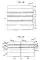
- Figure 2a is a diagrammatic representation of the layers a first gate structure in an integrated circuit with a barrier layer in accordance with an embodiment of the present invention.
- Figure 2b is a diagrammatic representation of the layers of a second gate structure in an integrated circuit with multiple barrier layers in accordance with an embodiment of the present invention.
- Figure 2c is a diagrammatic representation of a portion of a dual workfunction gate in accordance with an embodiment of the present invention.
- Figure 3 is a process flow diagram which illustrates the steps associated with one method of fabricating a gate structure in an integrated circuit with a barrier layer in accordance with an embodiment of the present invention.
- Figure 4a is a diagrammatic representation of a gate structure prior to the formation of a first silicon layer in accordance with an embodiment of the present invention.
- Figure 4b is a diagrammatic representation of the gate structure of Figure 4a after the formation of a first silicon layer in accordance with an embodiment of the present invention.
- Figure 4c is a diagrammatic representation of the gate structure of Figure 4b after an oxide layer has been deposited over the first silicon layer in accordance with an embodiment of the present invention.
- Figure 4d is a diagrammatic representation of the gate structure of Figure 4c after the oxide layer has been nitridized and etched in accordance with an embodiment of the present invention.
- Figure 4e is a diagrammatic representation of the gate structure of Figure 4d after a silicide layer has been deposited over the first silicon layer in accordance with an embodiment of the present invention.
- Figure 5 is a process flow diagram which illustrates the steps associated with a second method of fabricating a gate structure in an integrated circuit with a barrier layer in accordance with an embodiment of the present invention.
-
- The present invention will now be described in detail with reference to a few illustrative embodiments thereof as illustrated in the accompanying drawings. In the following description, numerous specific details are set forth in order to provide a thorough understanding of the present invention. It will be obvious, however, to one skilled in the art, that the present invention may be practiced without some or all of these specific details. In other instances, well known structures and steps have not been described in detail in order not to unnecessarily obscure the present invention.
- In order to reduce the amount of dopant outdiffusion into a silicide layer of a gate structure, e.g., a gate interconnect structure, during annealing processes, a barrier to diffusion is formed in accordance with one aspect of the present invention within the gate structure to impede the diffusion of dopants. Figure 2a is a diagrammatic representation of the layers a first gate structure in an integrated circuit with a barrier layer in accordance with an embodiment of the present invention. It should be appreciated that for illustrative purposes, some features of the gate structure have been exaggerated, while others have not been shown.
- As shown, a
gate structure 204 may be included as part of an integrated circuit. Such integrated circuit is, for example, a random access memory (RAM), a dynamic random access memory (DRAM), a synchronous DRAM (SDRAM), and a read only memory (ROM). Other integrated circuit such as an application specific integrated circuit (ASIC), a merged DRAM-logic circuit (embedded DRAM), or any other logic circuit is also useful. - Typically, numerous integrated circuits are formed on the wafer in parallel. After processing is finished, the wafer is diced to separate the integrated circuits to individual chips. The chips are then packaged, resulting in a final product that is used in, for example, consumer products such as computer systems, cellular phones, personal digital assistants (PDAs), and other electronic products.
- The gate structure is formed on a
substrate 206, such as silicon wafer. Other substrates such as gallium arsenide, germanium, silicon on insulator (SOI), or other semiconductor materials are also useful. The substrate, for example, may be lightly or heavily doped with dopants of a pre-determined conductivity to achieve the desired electrical characteristics.Substrate 206 may also include various other layers associated with the formation ofgate structure 204 or, more generally, the integrated circuit of whichgate structure 204 is a part. By way of example,substrate 206 may include insulating layers, conducting layers, and various junction regions, as will be appreciated by those skilled in the art. - A
gate oxide layer 208overlays substrate 206.Gate oxide layer 208 may generally be formed from any suitable material, as for example thermally grown oxide or nitrided oxides. Asilicon layer 210 is formed overgate oxide layer 208.Silicon layer 210, which may be a polycrystalline silicon layer, e.g, "polysilicon" layer, is doped using a do pant such as boron, phosphorous, or arsenic. Abarrier layer 212 lies oversilicon layer 210 and is, in the described embodiment, nitride which is located at the grain boundaries ofsilicon layer 210, e.g, withinsilicon layer 210 and especially near the top surface ofsilicon layer 210. -
Barrier layer 212 serves to reduce the amount of dopant that vertically and laterally outdiffuses fromsilicon layer 210 during annealing processes associated with creating a source or a drain usinggate structure 204. It should be appreciated thatbarrier layer 212 controls dopant diffusion during annealing while maintaining a low contact resistance.Barrier layer 212 generally maintains its integrity during the annealing at high temperature processing, e.g, processing at temperatures of greater than approximately 900 degrees Centigrade. - A silicide layer 216 is arranged over
barrier layer 212. In general, silicide layer 216 is low in resistance and, in one embodiment, silicide layer 216 may be formed from titanium silicide (TiSix). Other silicides, such as tungsten silicide (WSix), molybdenum silicide (MoSix), tantalum silicide (TaSix), cobalt silicide (CoSix), or any other silicides, are also useful. -
Barrier layer 212 reduces the amount of dopant which vertically diffuses fromsilicon layer 210 into silicide layer 216. Silicon layers 210, 214, together withbarrier layer 212, form alayered silicon structure 220. In general, layeredsilicon structure 220 may include substantially any number of silicon layers and barrier layers. A gate structure with a silicon structure which includes multiple silicon layers and barrier layers will be described in more detail below with respect to Figure 2b. - As shown,
gate structure 204 may also include adielectric layer 218 which is formed over silicide layer 216. In general,dielectric layer 218 may be used to insulate different layers ofgate structure 204 from other layers of the integrated circuit which includesgate structure 204. The dielectric layer may also serve as an etch stop layer for subsequent processing, such as to form a borderless contact. - The dimensions, e.g., thickness, of layers in
gate structure 204 may generally be widely varied. The thickness of each layer withingate structure 204 may depend upon the application in whichgate structure 204 is to be used. For example, the thicknesses of the layers may be smaller for 0.175 micron DRAM generation than for 0.25 micron DRAM generation. In one embodiment,gate oxide layer 208 may have a thickness in the range of approximately 30 Angstroms to approximately 100 Angstroms, e.g., approximately 60 Angstroms to approximately 65 Angstroms. In such an embodiment, the layered silicon structure may have a thickness in the range of approximately 1000 Angstroms to approximately 2000 Angstroms, while silicide layer 216 may have a thickness in the range of approximately 500 Angstroms to approximately 2000 Angstroms. - Referring next to Figure 2b, the composition of a second gate structure with multiple barrier layers will be described in accordance with an embodiment of the present invention. A
gate structure 234, likegate structure 204 of Figure 2a, may be included as part of an integrated circuit, e.g., a DRAM.Gate structure 234 includes asubstrate 206. Agate oxide layer 208overlays substrate 206. In the described embodiment, amulti-layered silicon structure 270 is formed overgate oxide layer 208. - Multi-layered silicon structure includes
multiple silicon layers silicon layer silicon layer 240, which substantially directly overlaysgate oxide layer 238, is doped using a dopant such as boron, phosphorous, or arsenic. Eachsilicon layer silicon layers silicon layer 240, e.g., doped using different dopants. It should be appreciated, however, than in other embodiments, substantially allsilicon layers - Barrier layers 242, 246 generally lie between
silicon layers barrier layer 242 lies betweensilicon layers barrier layer 246 lies betweensilicon layers barrier layer 242 which lies oversilicon layer 240, may be a film of nitride which is located at the grain boundaries near the top ofsilicon layer 240. In one embodiment,barrier layer 242 is formed using a nitridizing process, as will be discussed in more detail below with reference to Figure 3. -
Barrier layer 242 is arranged to reduce the amount of dopant that vertically outdiffuses fromsilicon layer 240 during annealing processes. The use of multiple barrier layers 242, 246, 250 essentially creates a matrix of barrier layers in or on layeredsilicon structure 270 to better control the overall amount of dopant which is essentially diffused out ofsilicon structure 270. In other words, by providing multiple barrier layers 242, 246, 250 withinsilicon structure 270, the vertical and lateral diffusion of dopants withingate structure 234 may be more readily controlled. - A
silicide layer 256, which may be formed from silicides which include, but are not limited to, titanium silicide and tungsten silicide. Barrier layers 242, 246, 250 withinsilicon structure 270, as mentioned above, reduce the amount of dopant which diffuses fromsilicon layer 240 intosilicide layer 256. In one embodiment,,gate structure 234 may include adielectric layer 258 which is formed oversilicide layer 256.Dielectric layer 258 may generally be used to insulate different layers ofgate structure 234 from other layers of an integrated circuit which includesgate structure 234. - Gate structures which use of barrier layers to control dopant outdiffusion may be used in a variety of different applications. As barrier layers may reduce both vertical diffusion to a silicide layer and lateral diffusion through the silicide layer, the use of gate structures with barrier layers is particularly useful in dual workfunction gates. Figure 2c is a diagrammatic representation of a portion of a dual workfunction gate in accordance with an embodiment of the present invention. For ease of illustration, some features of the dual workfunction gate have been exaggerated, while others have not been shown.
- A
dual workfunction gate 270 includes ajunction region 272 which may be a part of a semiconductor wafer substrate (not shown).Junction region 272 includes dopedregions region 272a comprises dopant of a first conductivity and the dopedregion 272b comprises dopant of a second conductivity. In the described embodiment,region 272a may be "p-doped," whileregion 272b may be "n-doped." Anundoped region 272c is located betweenregions region 272a from mixing with dopants inregion 272b. - As shown, a
gate oxide layer 276 is formed directly overjunction region 272. A first dopedsilicon layer 280 is located overgate oxide layer 276. In general, dopedregions Region 280a which indirectly overlaysregion 272a may be doped in the same manner asregion 272a, e.g., bothregion 272a andregion 280a may be p-doped, whileregion 280b andregion 272b, whichregion 280b indirectly overlays, may both be n-doped. - A
first barrier film 284 overlays dopedsilicon layer 280. The barrier layer comprises a material which is of sufficient thickness to prevent dopants in dopedsilicon layer 280 from laterally and vertically diffusing. In other words,first barrier film 284 obstructs the vertical and lateral diffusion of dopants therethrough during annealing processes. In one embodiment, the barrier comprises nitride at grain boundaries of dopedsilicon layer 280. - A
second silicon layer 288, which may or may not be doped, overlaysfirst barrier film 284. In one embodiment, as shown, asecond barrier film 290 overlayssecond silicon layer 288 to further control vertical diffusion of dopants. Silicon layers 280, 288, together withbarrier films - A
silicide layer 296 overlies silicon layer 292. Dopant diffusion intosilicide layer 296 is generally reduced through the use ofbarrier films silicide layer 296 may readily occur if dopants are allowed to vertically diffuse intosilicide layer 296. However, with the inclusion ofbarrier films silicide layer 296 and, hence, the amount of dopant which laterally diffuses throughsilicide layer 296 may be reduced. As a result,distinct regions 298a, 198b may be maintained indual workfunction gate 270. - In gate structures without barrier layers, the amount of dopant which diffuses, or migrates, into a silicide layer during annealing processes at temperatures of greater than approximately 800 degrees Centigrade has been observed as being greater than approximately 50 percent, as for example in the range of approximately 50 percent to approximately 70 percent, of the total amount of dopant in a doped silicon layer. With the use of barrier layers, the amount of dopant which diffuses into a silicide layer has been observed as being less than approximately 20 percent, e.g., in the range of approximately 4 percent to approximately 15 percent, of the total amount of dopant in a doped silicon layers.
- Figure 3 is a process flow diagram which illustrates the steps associated with one process which may be used to fabricate a gate structure, e.g.,
gate structure 204 of Figure 2a, which includes a barrier layer, in an integrated circuit in accordance with an embodiment of the present invention. Theprocess 302 begins atstep 304 where a substrate, e.g, a semiconductor wafer substrate, is provided. The substrate may generally be formed from silicon, and may further include various layers associated with the overall formation of an integrated circuit. Such layers may include, but are not limited to, metallization layers and oxide layers. - A gate oxide layer is deposited over the substrate in
step 306. Once the gate oxide layer is deposited, then process flow moves to step 308 where a silicon layer is deposited over the substrate or, more particularly, the gate oxide layer. In general as mentioned above, the silicon layer may be formed from any suitable silicon, as for example a polycrystalline silicon. The silicon layer, which is doped, may be doped using any suitable method, such as in situ doping or implantation of a dopant followed by an annealing process, as will be appreciated by those skilled in the art. While dopants used to dope the silicon layer may be widely varied, in one embodiment, dopants include phosphorous, boron, and arsenic. - A barrier layer is then formed on the polysilicon layer in
Step 310. The barrier layer includes, for example, an oxide layer The oxide layer, which may be a silicon dioxide (SiO2) layer, may be grown on the surface of the silicon layer using any suitable method. Typically, the oxide layer may be grown using a rapid thermal oxidation (RTO) in oxygen at a temperature in the range of approximately 900 degrees Centigrade to approximately 1100 degrees Centigrade, as for example approximately 925 degrees Centigrade, for a time duration in the range of approximately 30 seconds to approximately 120 seconds, as for example approximately 60 seconds. While the thickness of the oxide layer may be widely varied, in one embodiment, the thickness of the oxide layer is in the range of approximately 40 Angstroms to approximately 50 Angstroms. - Once the oxide layer is grown in
step 310, process flow proceeds to step 312 in which a nitridization process is performed on the oxide layer. In other words, the oxide is nitridized. Oxide may generally be nitridized using any suitable method, such as a rapid thermal nitridization (RTN) using ammonia (NH3), or other suitable nitrogen-contained gases, at a temperature in the range of approximately 900 degrees Centigrade to approximately 1100 degrees Centigrade, e.g., approximately 1050 degrees Centigrade, for a duration in the range of approximately 20 seconds to 120 seconds, e.g., approximately 30 seconds. - When the oxide layer is nitridized, nitride, e.g., silicon nitride (SiNx), forms on the surface of the silicon layer and at the grain boundaries of the silicon layer. That is, an SiNx film forms at the interface between the oxide layer and at the grain boundaries the underlying silicon layer. In general, nitride diffuses along the grain boundaries of the silicon layer. In some embodiments, as for example when the thickness of the silicon layer is relatively thin, nitride may permeate substantially the entire silicon layer when the oxide layer is nitridized. When nitride permeates substantially the entire silicon layer, both vertical dopant diffusion and lateral dopant diffusion may be significantly reduced, as for example in a dual workfunction gate, as described above with respect to Figure 2c.
- After the nitridization on the oxide layer is completed, the nitridized oxide layer is stnpped, or otherwise etched, to expose nitrogen at the grain boundaries of the silicon layer in
step 314. The exposed nitrogen at the grain boundaries forms a barrier layer which prevents dopant diffusion in a vertical direction between the underlying silicon layer and layers which overlay the silicon layer. It should be appreciated that the barrier layer may also reduce the amount of dopant diffusion in a lateral direction. - A determination is made in
step 318 regarding whether additional silicon layers are to be formed over the new silicon layer. If the determination is that additional silicon layers are to be formed, the indication is that a thicker, "overall" silicon layer is desired within the gate structure. In general, the overall silicon layer is a layered structure, as the overall silicon layer includes at least two individual silicon layers with a barrier layer formed therebetween. In one embodiment, a thicker overall silicon layer may be used to provide a plurality of barrier layers in a gate structure to further reduce the amount of both vertical and lateral diffusion within the gate structure. In another embodiment, a silicon layer which includes an individual silicon layer with a barrier film over it may be used to reduce both vertical and lateral diffusion. - If the determination in
step 318 is that at least one additional silicon layer is to be formed over the existing silicon layers, then process flow returns to step 308 where a new silicon layer is formed over the substrate or, more specifically, over the barrier layer. Alternatively, when the determination is that no additional silicon layers are to be formed, then process flow moves to step 320 in which a silicide layer is deposited over the silicon layers. Then instep 322, additional processing is performed to complete the processing of the gate structure. In general, the additional processing may include, but is not limited to, depositing in insulating layer, e.g, a dielectric layer, over the silicide layer, lithographic patterning dry etching sidewall spacer formation, and junction doping. Once the additional processing is completed, then the process of fabricating a gate structure is completed. - Referring next to Figures 4a-4e, the fabrication of a gate structure, using the steps described above with respect to Figure 3, will be described in accordance with an embodiment of the present invention. It should be appreciated that for illustrative purposes, some features of the gate structure, particularly the size of a barrier layer, have been exaggerated, while others have not been shown. The fabrication of a
gate structure 402 begins with the formation of asubstrate 404. Agate oxide layer 408 is formed over the substrate. - A doped
silicon layer 412 is formed overgate oxide layer 408. Anoxide layer 416 is deposited over the dopedsilicon layer 412 to promote the formation of a barrier layer. During a nitridization of theoxide layer 416, as described above with respect to Figure 3, nitride is essentially implanted at thegrain boundaries 414 of dopedsilicon layer 412. After theoxide layer 416 is striped away, a barrier layer 414', which may be a film, that is formed at thegrain boundaries 414 of dopedsilicon layer 412, is exposed. Asilicide layer 422 is deposited over barrier layer 414'. In general, various other layers may be associated withgate structure 402, including a dielectric layer (not shown) which is often deposited oversilicide layer 422. - With reference to Figure 5, a second process which may be used to fabricate a gate structure that includes a barrier layer will be described in accordance with an embodiment of the present invention. The
process 502 begins atstep 504 in which a substrate is formed. The substrate may include various layers associated with the overall formation of an integrated circuit of which the gate structure is a part. - After the substrate is formed, a gate oxide layer is deposited over the substrate in
step 506. A silicon layer is deposited over the substrate or, more particularly, the gate oxide layer instep 508. In general, the silicon layer is a doped silicon layer which may be, but is not limited to being, a doped polycrystalline silicon layer. - Once the silicon layer is deposited, an oxynitride film is deposited over the silicon layer using a chemical vapor deposition process in
step 510. As will be appreciated by those skilled in the art, a variety of different chemical vapor deposition processes, including low pressure chemical vapor deposition (LPCVD) and plasma enhanced chemical vapor deposition (PECVD), may be used to deposit the oxynitride film. - The oxynitride layer is stripped, or otherwise etched, to expose nitrogen at the grain boundaries of the silicon layer in
step 512. The exposed nitrogen at the grain boundaries forms a barrier layer which prevents dopant diffusion in a vertical direction between the underlying silicon layer and a subsequent layers which are deposited over the grain boundaries. It should be appreciated that the barrier layer may also reduce the amount of dopant diffusion in a lateral direction. - A determination is made in
step 516 regarding whether additional silicon layers are to be formed over the barrier layer. If the determination instep 516 is that at least one additional silicon layer is to be formed over the existing silicon layers, then process flow returns to step 508, where a new silicon layer is formed over the substrate or, more specifically, the barrier layer. Alternatively, when the determination is that no additional silicon layers are to be formed, then process flow moves to step 518 in which a silicide layer is deposited over the barrier layer. Finally, instep 520, additional processing is performed to complete the processing of the gate structure. In general, the additional processing may include, but is not limited to, depositing an insulating layer, e.g., a dielectric layer, over the silicide layer, lithography, etching, and junction doping. Once the additional processing is completed, the second process of fabricating a gate structure is completed. - Although only a few embodiments of the present invention have been described, it should be understood that the present invention may be embodied in many other specific forms without departing from the spirit or the scope of the invention. By way of example, a gate structure which includes a barrier layer has been described as being suitable for use in the fabrication of a dual workfunction gate that may be include in an integrated circuit such as a dynamic random access memory (DRAM). In general, however, the gate structure which includes a barrier layer may be suitable for use in a variety of other applications.
- The creation of a barrier layer has been described as using either an oxide layer which is nitridized then etched, or an oxynitride layer which is deposited using a process such as CVD then etched. However, it should be appreciated that any suitable method may generally be used to create a barrier layer within a layered silicon structure without departing from the spirit or the scope of the present invention.
- As previously mentioned, the silicon layers in a gate interconnect structure, such as a gate interconnect structure in a dual workfunction gate, may be formed from any suitable silicon. For example, in one embodiment, the silicon layers may be polycrystalline silicon layers. Similarly, the barrier layer may also be created using substantially any material which controls dopant outdiffusion from a doped silicon layer.
- In general, a layered silicon structure may include any number of different silicon layers. The number of silicon layers in the silicon structure is generally dependent upon the overall desired thickness of the silicon structure, as well as the thickness of the individual layers and the barrier layers. As described above, the overall thickness of the silicon structure may be widely varied. By way of example, the thickness may be in the range of approximately 1000 Angstroms to approximately 2000 Angstroms. Similarly, the thicknesses of the silicon layers and the barrier layers may also be widely varied. In one embodiment, the thickness of each silicon layer may be in the range of approximately 100 Angstroms to approximately 500 Angstroms, while the thickness of each barrier layer may be in the range of approximately 50 Angstroms to approximately 30 Angstroms.
- While the silicon layer which substantially directly overlays a gate oxide layer is generally doped, subsequent silicon layers are not necessarily doped. When some of the subsequent silicon layers are doped, those silicon layers are often doped differently from the silicon layer which substantially contacts the gate oxide layer.
- Further, the top-most barrier layer of a layered silicon structure has been described as being the top layer of the silicon structure, i.e., the layer over which silicide is typically directly deposited. However, it should be appreciated that the top-most barrier layer may also be "sandwiched" between silicon layers without departing from the spirit or the scope of the present invention. Therefore, the present examples are to be considered as illustrative and not restrictive, and the invention is not to be limited to the details given herein, but may be modified within the scope of the appended claims along with their full scope of equivalents.
Claims (21)
- A method for minimizing dopant outdiffusion within an integrated circuit, the method comprising:forming a substrate;forming a gate oxide layer at least partially over the substrate ;forming a layered silicon structure over the gate oxide layer, the layered silicon structure being arranged to impede dopant diffusion; andforming a silicide layer over the layered silicon structure.
- A method as recited in claim 1 wherein forming a layered silicon structure includes:depositing a first doped silicon layer over the gate oxide layer;forming a first oxide layer over the first silicon layer;nitridizing the first oxide layer; andetching the nitridized first oxide layer, wherein etching the nitridized first oxide layer exposes nitride at grain boundaries of the first silicon.
- A method as recited in claim 2 wherein nitridizing the first oxide layer diffuses nitrogen into the first doped silicon layer.
- A method as recited in claim 3 wherein:forming the first oxide layer over the first silicon layer includes growing the first oxide layer at a first process temperature in the range of approximately 900 degrees Centigrade to approximately 1000 degrees Centigrade; andnitridizing the oxide layer includes nitridizing the oxide layer at a second process temperature in the range of approximately 900 degrees Centigrade to approximately 1100 degrees Centigrade.
- A method as recited in claim 2 further including;depositing a second silicon layer over the nitride exposed at the grain boundaries of the first silicon layer;forming a second oxide layer over the second silicon layer;nitridizing the second oxide layer; andetching the nitridized second oxide layer, wherein etching the nitridized second oxide layer exposes nitride at a grain boundaries of the second silicon layer.
- A method as recited in claim 1 wherein forming a layered silicon structure includes:depositing a first doped silicon layer over the gate oxide layer,performing a chemical vapor deposition to form an oxynitride film over the first doped silicon layer; andetching the oxynitride film, wherein etching the oxynitride film exposes nitride at a grain boundaries of the first silicon layer.
- A gate structure on an integrated circuit chip comprising:a substrate, wherein the substrate includes a junction region;a gate oxide layer formed at least partially over the junction region of the substrate;a layered silicon structure formed over the gate oxide layer, wherein the layered silicon structure is arranged to reduce diffusion within the gate structure; anda silicide layer formed over the layered silicon structure.
- A gate structure as recited in claim 7 wherein the layered silicon structure includes at least a first doped silicon layer.
- A gate structure as recited in claim 8 wherein the layered silicon structure further includes a barrier film disposed between the first silicon layer and the silicide layer.
- A gate structure as recited in claim 9 wherein the barrier film has a thickness in the range of approximately 50 Angstroms to approximately 80 Angstroms.
- A gate structure as recited in claim 9 wherein the barrier film includes silicon oxynitride.
- A gate structure as recited in claim 9 wherein the gate structure is a dual workfunction gate and the integrated circuit is a digital random access memory integrated circuit.
- A gate structure as recited in claim 8 wherein the first silicon layer is doped using a dopant selected from the group consisting of boron, phosphorous, and arsenic.
- A gate structure as recited in claim 9 further wherein the layered silicon structure further includes:a second silicon layer disposed between the barrier film and the silicide layer; anda second barrier film disposed between the second silicon layer and the silicide layer.
- A gate structure as recited in claim 14 wherein the layered silicon structure includes a first doped polysilicon layer and a second polysilicon layer.
- A gate structure as recited in claim 7 wherein the layered silicon structure has a thickness in the range of approximately 1000 Angstroms to approximately 1500 Angstroms.
- A gate structure on an integrated circuit chip comprising:a substrate;a gate oxide layer formed at least partially over the substrate;a layered silicon structure formed over the gate oxide layer, wherein the layer silicon structure inciudes a first doped silicon layer and a first barrier film, the first barrier film being arranged to prevent the first doped silicon layer from outdiffusing; anda silicide layer formed over the layered silicon structure.
- A gate structure as recited in claim 17 wherein the layered silicon structure includes a second silicon layer.
- A gate structure as recited in claim 18 wherein the layered silicon structure further includes a second barrier film arranged over the second silicon layer.
- A gate structure as recited in claim 19 wherein the integrated circuit is a digital random access memory integrated circuit.
- An integrated circuit including a gate structure as defined in any of claims 7 to 20.
Applications Claiming Priority (2)
| Application Number | Priority Date | Filing Date | Title |
|---|---|---|---|
| US93920997A | 1997-09-29 | 1997-09-29 | |
| US939209 | 1997-09-29 |
Publications (3)
| Publication Number | Publication Date |
|---|---|
| EP0905751A2 true EP0905751A2 (en) | 1999-03-31 |
| EP0905751A3 EP0905751A3 (en) | 1999-08-11 |
| EP0905751B1 EP0905751B1 (en) | 2006-12-13 |
Family
ID=25472745
Family Applications (1)
| Application Number | Title | Priority Date | Filing Date |
|---|---|---|---|
| EP98307025A Expired - Lifetime EP0905751B1 (en) | 1997-09-29 | 1998-09-01 | Method for minimizing lateral and vertical dopant diffusion in gate structures |
Country Status (7)
| Country | Link |
|---|---|
| US (1) | US5998253A (en) |
| EP (1) | EP0905751B1 (en) |
| JP (1) | JPH11163160A (en) |
| KR (1) | KR19990030078A (en) |
| CN (1) | CN1155056C (en) |
| DE (1) | DE69836607T2 (en) |
| TW (1) | TW402747B (en) |
Cited By (2)
| Publication number | Priority date | Publication date | Assignee | Title |
|---|---|---|---|---|
| EP0903776A2 (en) * | 1997-09-23 | 1999-03-24 | International Business Machines Corporation | Titanium polycide stabilization with a porous barrier |
| EP0986095A2 (en) * | 1998-09-08 | 2000-03-15 | Siemens Aktiengesellschaft | Layered structure with a material layer and a diffusion barrier layer disposed at the grain boundary of the material layer and process for fabricating the same |
Families Citing this family (20)
| Publication number | Priority date | Publication date | Assignee | Title |
|---|---|---|---|---|
| US6767794B2 (en) * | 1998-01-05 | 2004-07-27 | Advanced Micro Devices, Inc. | Method of making ultra thin oxide formation using selective etchback technique integrated with thin nitride layer for high performance MOSFET |
| US6309924B1 (en) | 2000-06-02 | 2001-10-30 | International Business Machines Corporation | Method of forming self-limiting polysilicon LOCOS for DRAM cell |
| US6649543B1 (en) * | 2000-06-22 | 2003-11-18 | Micron Technology, Inc. | Methods of forming silicon nitride, methods of forming transistor devices, and transistor devices |
| US6686298B1 (en) | 2000-06-22 | 2004-02-03 | Micron Technology, Inc. | Methods of forming structures over semiconductor substrates, and methods of forming transistors associated with semiconductor substrates |
| US6833329B1 (en) | 2000-06-22 | 2004-12-21 | Micron Technology, Inc. | Methods of forming oxide regions over semiconductor substrates |
| US6660657B1 (en) | 2000-08-07 | 2003-12-09 | Micron Technology, Inc. | Methods of incorporating nitrogen into silicon-oxide-containing layers |
| US6383943B1 (en) * | 2000-10-16 | 2002-05-07 | Taiwan Semiconductor Manufacturing Company | Process for improving copper fill integrity |
| US6495475B2 (en) | 2001-03-28 | 2002-12-17 | Atmel Corporation | Method for fabrication of a high capacitance interpoly dielectric |
| US6653678B2 (en) | 2001-07-13 | 2003-11-25 | International Business Machines Corporation | Reduction of polysilicon stress in trench capacitors |
| US6878585B2 (en) * | 2001-08-29 | 2005-04-12 | Micron Technology, Inc. | Methods of forming capacitors |
| US6723599B2 (en) | 2001-12-03 | 2004-04-20 | Micron Technology, Inc. | Methods of forming capacitors and methods of forming capacitor dielectric layers |
| TW566366U (en) * | 2002-09-27 | 2003-12-11 | Wus Tech Co Ltd | Labor-saving portable battery equipment for power-driven walking assisted scooter |
| US6979851B2 (en) * | 2002-10-04 | 2005-12-27 | International Business Machines Corporation | Structure and method of vertical transistor DRAM cell having a low leakage buried strap |
| US7138691B2 (en) * | 2004-01-22 | 2006-11-21 | International Business Machines Corporation | Selective nitridation of gate oxides |
| US7898014B2 (en) * | 2006-03-30 | 2011-03-01 | International Business Machines Corporation | Semiconductor device structures with self-aligned doped regions and methods for forming such semiconductor device structures |
| US20080048186A1 (en) * | 2006-03-30 | 2008-02-28 | International Business Machines Corporation | Design Structures Incorporating Semiconductor Device Structures with Self-Aligned Doped Regions |
| JP4685953B2 (en) * | 2009-07-17 | 2011-05-18 | Dowaエレクトロニクス株式会社 | EPITAXIAL SUBSTRATE FOR ELECTRONIC DEVICES WITH VERTICAL DIRECTION OF CURRENT CONDUCTION |
| CN103578998B (en) * | 2012-07-30 | 2016-06-08 | 上海华虹宏力半导体制造有限公司 | Prevent the method that in PMOS device technique, grid polycrystalline silicon exhausts |
| CN103681341B (en) * | 2012-09-21 | 2016-04-13 | 上海华虹宏力半导体制造有限公司 | Suppress the method for PMOS device threshold voltage shift |
| US9240354B2 (en) | 2012-11-14 | 2016-01-19 | Globalfoundries Inc. | Semiconductor device having diffusion barrier to reduce back channel leakage |
Citations (4)
| Publication number | Priority date | Publication date | Assignee | Title |
|---|---|---|---|---|
| US4935804A (en) * | 1984-03-19 | 1990-06-19 | Fujitsu Limited | Semiconductor device |
| EP0682359A1 (en) * | 1994-05-09 | 1995-11-15 | International Business Machines Corporation | Multilayer gate MOS device |
| EP0780889A2 (en) * | 1995-12-22 | 1997-06-25 | France Telecom | Method for selective depositing of refractory metal silicide on silicon and silicon wafer metallized by this process |
| EP0903776A2 (en) * | 1997-09-23 | 1999-03-24 | International Business Machines Corporation | Titanium polycide stabilization with a porous barrier |
Family Cites Families (6)
| Publication number | Priority date | Publication date | Assignee | Title |
|---|---|---|---|---|
| US5103276A (en) * | 1988-06-01 | 1992-04-07 | Texas Instruments Incorporated | High performance composed pillar dram cell |
| US4952524A (en) * | 1989-05-05 | 1990-08-28 | At&T Bell Laboratories | Semiconductor device manufacture including trench formation |
| US5218218A (en) * | 1990-02-01 | 1993-06-08 | Mitsubishi Denki Kabushiki Kaisha | Semiconductor device and manufacturing method thereof |
| KR940006679B1 (en) * | 1991-09-26 | 1994-07-25 | 현대전자산업 주식회사 | Dram cell having a vertical transistor and fabricating method thereof |
| KR970009276B1 (en) * | 1993-10-28 | 1997-06-09 | 금성일렉트론 주식회사 | Method for manufacturing moset |
| JP2817645B2 (en) * | 1995-01-25 | 1998-10-30 | 日本電気株式会社 | Method for manufacturing semiconductor device |
-
1997
- 1997-12-19 US US08/993,743 patent/US5998253A/en not_active Expired - Lifetime
-
1998
- 1998-08-18 TW TW087113545A patent/TW402747B/en not_active IP Right Cessation
- 1998-08-26 CN CNB98118734XA patent/CN1155056C/en not_active Expired - Fee Related
- 1998-09-01 EP EP98307025A patent/EP0905751B1/en not_active Expired - Lifetime
- 1998-09-01 DE DE69836607T patent/DE69836607T2/en not_active Expired - Fee Related
- 1998-09-24 KR KR1019980039560A patent/KR19990030078A/en not_active Application Discontinuation
- 1998-09-25 JP JP10271473A patent/JPH11163160A/en active Pending
Patent Citations (4)
| Publication number | Priority date | Publication date | Assignee | Title |
|---|---|---|---|---|
| US4935804A (en) * | 1984-03-19 | 1990-06-19 | Fujitsu Limited | Semiconductor device |
| EP0682359A1 (en) * | 1994-05-09 | 1995-11-15 | International Business Machines Corporation | Multilayer gate MOS device |
| EP0780889A2 (en) * | 1995-12-22 | 1997-06-25 | France Telecom | Method for selective depositing of refractory metal silicide on silicon and silicon wafer metallized by this process |
| EP0903776A2 (en) * | 1997-09-23 | 1999-03-24 | International Business Machines Corporation | Titanium polycide stabilization with a porous barrier |
Non-Patent Citations (3)
| Title |
|---|
| "PROCESS FOR SUPPRESSION OF ANOMALOUS SUB-THRESHOLD LEAKAGE" IBM TECHNICAL DISCLOSURE BULLETIN, vol. 37, no. 11, 1 November 1994, page 177 XP000487204 * |
| HOSOYA T ET AL: "A POLYCIDE GATE ELECTRODE WITH A CONDUCTIVE DIFFUSION BARRIER FORMED WITH ECR NITROGEN PLASMA FOR DUAL GATE CMOS" IEEE TRANSACTIONS ON ELECTRON DEVICES, vol. 42, no. 12, 1 December 1995, pages 2111-2116, XP000582420 * |
| KAZUHIRO KOBUSHI ET AL: "A HIGH INTEGRITY AND LOW RESISTANCE TI-POLYCIDE GATE USING A NITROGEN ION-IMPLANTED BUFFER LAYER" JAPANESE JOURNAL OF APPLIED PHYSICS, vol. 27, no. 11, 1 November 1988, pages 2158-2160, XP000068677 * |
Cited By (5)
| Publication number | Priority date | Publication date | Assignee | Title |
|---|---|---|---|---|
| EP0903776A2 (en) * | 1997-09-23 | 1999-03-24 | International Business Machines Corporation | Titanium polycide stabilization with a porous barrier |
| EP0903776A3 (en) * | 1997-09-23 | 1999-08-11 | International Business Machines Corporation | Titanium polycide stabilization with a porous barrier |
| US6057220A (en) * | 1997-09-23 | 2000-05-02 | International Business Machines Corporation | Titanium polycide stabilization with a porous barrier |
| EP0986095A2 (en) * | 1998-09-08 | 2000-03-15 | Siemens Aktiengesellschaft | Layered structure with a material layer and a diffusion barrier layer disposed at the grain boundary of the material layer and process for fabricating the same |
| EP0986095A3 (en) * | 1998-09-08 | 2005-08-17 | Infineon Technologies AG | Layered structure with a material layer and a diffusion barrier layer disposed at the grain boundary of the material layer and process for fabricating the same |
Also Published As
| Publication number | Publication date |
|---|---|
| TW402747B (en) | 2000-08-21 |
| JPH11163160A (en) | 1999-06-18 |
| EP0905751A3 (en) | 1999-08-11 |
| CN1213845A (en) | 1999-04-14 |
| US5998253A (en) | 1999-12-07 |
| KR19990030078A (en) | 1999-04-26 |
| EP0905751B1 (en) | 2006-12-13 |
| CN1155056C (en) | 2004-06-23 |
| DE69836607T2 (en) | 2007-10-11 |
| DE69836607D1 (en) | 2007-01-25 |
Similar Documents
| Publication | Publication Date | Title |
|---|---|---|
| EP0905751B1 (en) | Method for minimizing lateral and vertical dopant diffusion in gate structures | |
| US6465335B1 (en) | Method of manufacturing semiconductor device | |
| US6130145A (en) | Insitu doped metal policide | |
| US7902614B2 (en) | Semiconductor device with gate stack structure | |
| US5904564A (en) | Method for fabricating MOSFET having cobalt silicide film | |
| US6329277B1 (en) | Method of forming cobalt silicide | |
| US8319341B2 (en) | Semiconductor device with gate structure | |
| EP0926717B1 (en) | Method of forming polysilicon capacitor electrode | |
| EP0905750B1 (en) | Reliable polycide gate stack with reduced sheet resistance | |
| US6333220B1 (en) | Method and apparatus for providing low-GIDL dual workfunction gate doping with borderless diffusion contact | |
| KR100265677B1 (en) | Semiconductor device having oxygen-doped silicon layer so as to restrict diffusion from heavily doped silicon layer and process of fabrication thereof | |
| JPH1093077A (en) | Semiconductor device and manufacturing method thereof | |
| US6197672B1 (en) | Method for forming polycide dual gate | |
| JP2001203347A (en) | Semiconductor device and manufacturing method | |
| KR100744642B1 (en) | Metal line of semiconductor device, gate electrode of semiconductor device and method forming the gate electrode | |
| KR20080039143A (en) | W-dual poly gate and manufacturing method of the same | |
| JPH06151754A (en) | Semiconductor memory device | |
| JPH04239180A (en) | Manufacture of non-volatile semiconductor memory |
Legal Events
| Date | Code | Title | Description |
|---|---|---|---|
| PUAI | Public reference made under article 153(3) epc to a published international application that has entered the european phase |
Free format text: ORIGINAL CODE: 0009012 |
|
| AK | Designated contracting states |
Kind code of ref document: A2 Designated state(s): DE FR GB IE IT NL |
|
| AX | Request for extension of the european patent |
Free format text: AL;LT;LV;MK;RO;SI |
|
| PUAL | Search report despatched |
Free format text: ORIGINAL CODE: 0009013 |
|
| AK | Designated contracting states |
Kind code of ref document: A3 Designated state(s): AT BE CH CY DE DK ES FI FR GB GR IE IT LI LU MC NL PT SE |
|
| AX | Request for extension of the european patent |
Free format text: AL;LT;LV;MK;RO;SI |
|
| RIC1 | Information provided on ipc code assigned before grant |
Free format text: 6H 01L 21/28 A, 6H 01L 29/49 B, 6H 01L 21/768 B, 6H 01L 21/8238 B |
|
| 17P | Request for examination filed |
Effective date: 20000210 |
|
| AKX | Designation fees paid |
Free format text: DE FR GB IE IT NL |
|
| RAP1 | Party data changed (applicant data changed or rights of an application transferred) |
Owner name: INTERNATIONAL BUSINESS MACHINES CORPORATION Owner name: INFINEON TECHNOLOGIES AG |
|
| 17Q | First examination report despatched |
Effective date: 20040601 |
|
| GRAP | Despatch of communication of intention to grant a patent |
Free format text: ORIGINAL CODE: EPIDOSNIGR1 |
|
| REG | Reference to a national code |
Ref country code: HK Ref legal event code: WD Ref document number: 1018981 Country of ref document: HK |
|
| RIC1 | Information provided on ipc code assigned before grant |
Ipc: H01L 21/8238 20060101ALI20060323BHEP Ipc: H01L 21/28 20060101AFI20060323BHEP |
|
| GRAS | Grant fee paid |
Free format text: ORIGINAL CODE: EPIDOSNIGR3 |
|
| RAP1 | Party data changed (applicant data changed or rights of an application transferred) |
Owner name: INTERNATIONAL BUSINESS MACHINES CORPORATION Owner name: QIMONDA AG |
|
| GRAA | (expected) grant |
Free format text: ORIGINAL CODE: 0009210 |
|
| AK | Designated contracting states |
Kind code of ref document: B1 Designated state(s): DE FR GB IE IT NL |
|
| PG25 | Lapsed in a contracting state [announced via postgrant information from national office to epo] |
Ref country code: NL Free format text: LAPSE BECAUSE OF FAILURE TO SUBMIT A TRANSLATION OF THE DESCRIPTION OR TO PAY THE FEE WITHIN THE PRESCRIBED TIME-LIMIT Effective date: 20061213 |
|
| REG | Reference to a national code |
Ref country code: GB Ref legal event code: FG4D |
|
| REG | Reference to a national code |
Ref country code: IE Ref legal event code: FG4D |
|
| REF | Corresponds to: |
Ref document number: 69836607 Country of ref document: DE Date of ref document: 20070125 Kind code of ref document: P |
|
| NLV1 | Nl: lapsed or annulled due to failure to fulfill the requirements of art. 29p and 29m of the patents act | ||
| ET | Fr: translation filed | ||
| PLBE | No opposition filed within time limit |
Free format text: ORIGINAL CODE: 0009261 |
|
| STAA | Information on the status of an ep patent application or granted ep patent |
Free format text: STATUS: NO OPPOSITION FILED WITHIN TIME LIMIT |
|
| 26N | No opposition filed |
Effective date: 20070914 |
|
| PGFP | Annual fee paid to national office [announced via postgrant information from national office to epo] |
Ref country code: GB Payment date: 20070914 Year of fee payment: 10 |
|
| PGFP | Annual fee paid to national office [announced via postgrant information from national office to epo] |
Ref country code: DE Payment date: 20071113 Year of fee payment: 10 |
|
| PG25 | Lapsed in a contracting state [announced via postgrant information from national office to epo] |
Ref country code: IE Free format text: LAPSE BECAUSE OF NON-PAYMENT OF DUE FEES Effective date: 20070903 |
|
| PGFP | Annual fee paid to national office [announced via postgrant information from national office to epo] |
Ref country code: IT Payment date: 20080924 Year of fee payment: 11 Ref country code: FR Payment date: 20080912 Year of fee payment: 11 |
|
| GBPC | Gb: european patent ceased through non-payment of renewal fee |
Effective date: 20080901 |
|
| PG25 | Lapsed in a contracting state [announced via postgrant information from national office to epo] |
Ref country code: DE Free format text: LAPSE BECAUSE OF NON-PAYMENT OF DUE FEES Effective date: 20090401 |
|
| PG25 | Lapsed in a contracting state [announced via postgrant information from national office to epo] |
Ref country code: GB Free format text: LAPSE BECAUSE OF NON-PAYMENT OF DUE FEES Effective date: 20080901 |
|
| REG | Reference to a national code |
Ref country code: FR Ref legal event code: ST Effective date: 20100531 |
|
| PG25 | Lapsed in a contracting state [announced via postgrant information from national office to epo] |
Ref country code: FR Free format text: LAPSE BECAUSE OF NON-PAYMENT OF DUE FEES Effective date: 20090930 |
|
| PG25 | Lapsed in a contracting state [announced via postgrant information from national office to epo] |
Ref country code: IT Free format text: LAPSE BECAUSE OF NON-PAYMENT OF DUE FEES Effective date: 20090901 |