FIELD OF THE INVENTION
-
The present invention relates to a disk array device
adapted to execution of data I/O processing by concurrently
accessing a plurality units of disk device, and more
specifically a disk array device adapted for maintenance of
consistency of data by executing, when write processing is
interrupted due to, for instance, power failure, recovery
processing for data write using the data stored therein.
BACKGROUND OF THE INVENTION
-
A disk device having nonvolatability of record, a large capacity,
a capability for high speed data transfer or other excellent
features such as a magnetic disk or an optical disk device has
been widely used as an external storage device for a computer
system. Demands for a disk device include those for a
capability for high speed data transfer, high reliability, a
large capacity, and a low price. As a disk device satisfying
the requirements as described above, now hot attentions are put
gathered on a disk array device. The disk array device
comprises a plurality of compact disk devices for recording
therein data distributedly and also for enabling concurrent
access to the data.
-
With the disk array device, by concurrently executing
data transfer to a plurality of disk devices, data transfer can
be executed at a rate higher by the number of disk devices as
compared to a data transfer rate in a case of a single disk device.
Further, by recording, in addition to data, redundant
information such as parity data, it becomes possible to detect
and correct a data error caused by, for instance, a failure of
a disk device, and the reliability as high as that obtained in
the method of recording duplicated contents of a disk device
with a lower cost as compared to that requiring for duplicating.
-
It is generally recognized that a disk array device is
a new recording medium simultaneously satisfying the three
requirements for low price, high speed, and high reliability.
For this reason, it is not allowable that any of the three
requirements is not satisfied. What is most important and most
difficult to maintain is high reliability. For, a signal disk
itself constituting a disk array is a cheap one, and so high
reliability is not required to a single disk itself.
Accordingly, to realize a disk array device, it is most required
to maintain the high reliability, and the present invention
relates to a disk array device, so that the factor of high
reliability is especially important.
-
David A. Patterson of Barkley school, California
University, et al. have published reports in which disk array
devices each for distributing a large volume of data to a number
of disks at a high speed for realizing redundancy of data in
preparation for a failure of any disk are classified to levels
1 to 5 (ACM SIGMOD Conference, Chicago, Illinois, June 1-3, 1988,
p109 to p116).
-
The levels 1 to 5 used for classification of disk array
devices proposed by David A. Patternson et al. is abbreviated
as RAID (Redundant Arrays of Inexpensive Disks). Next brief
description is made for RAID 1 to 5.
-
Fig. 32 shows a disk array device not having data
redundancy, and this category is not included in the levels
proposed by David A. Patterson et al., but this level is
described herein as RAID0. In a RAID0 disk array device, as
shown by data A to I, a disk array control unit 10 distributes
data to disk devices 32-1 to 32-3 according to an I/O request
from a host computer 18, and data redundancy for disk error is
not insured.
-
A RAID1 disk array device has, as shown in Fig. 33, a mirror
disk device 32-2 in which copies A' to C' of data A to C stored
in the disk device 32-1 are stored. In a case of RAID1, use
efficiency of the disk device is low, but data redundancy is
insured, and can be realized with simple controls, so that this
type of disk array device has widely been used.
-
A RAID2 disk array device stripes (divides) data by a unit
of bit or byte, and concurrently executes data write or data
read to and from each disk device. The striped data is recorded
in the physically same sectors in all the disk devices. As error
correction code, hamming code generated from data is used. The
RAID2 disk array device has, in addition to disk devices for
data storage, a disk device for recording the hamming code
therein, and identifies a faulty disk from the hamming code to
restore data. By having data redundancy based on hamming code,
data can be insured even if a disk device goes wrong, but the
use efficiency of disk devices is rather low, so that this type
of disk array device has not been put into practical use.
-
A RAID3 disk array device has the configuration as shown
in Fig. 34. Namely, as shown in Fig. 35, for instance, data
a, b, c are divided by a unit of bit or sector to data a1 to
a3, b1 to b3, and c1 to c3, and further parity P1 is computed
from the data a1 to a3, parity P2 is computed from the data b1
to b3, and also parity P3 is computed from data c1 to c3, and
the disk devices 32-1 to 32-4 shown in Fig. 34 are concurrently
accessed to write data therein.
-
In a case of RAID3, redundancy of data is maintained with
parity. Further a time required for data write can be reduced
by concurrently processing divided data. However, a
concurrent seek operation is required for all the disk devices
32-1 to 32-4 for each access for data write or data read. This
scheme is effective when a large volume of data is continuously
treated, but in a case of, for instance, transaction processing
for accessing a small volume of data at random, the capability
for high-speed data transfer can not effectively be used, and
the efficiency goes lower.
-
A RAID4 disk array device divides one piece of data by
sector and then writes the divided data in the same disk device.
For instance, in the disk device 32-1, data a is divided to sector
data a1 to a4 and the divided data is written therein. The
parity is stored in a disk device 32-4 univocally decided.
Herein parity P1 is computed from data a1, b1, and c1, parity
P2 from data a2, b2, c2, parity P3 from data a3, b3, c3, and
parity P4 from data a4, b4, c4.
-
Data can concurrently be read from the disk devices 32-1
to 32-3. As for an operation for reading data a to b, in a case
of the data a, sector data a1 to a4 are successively read out
and synthesized by accessing sectors 0 to 3 of the disk device
32-1. When writing data, data prior to write processing and
the parity are read and then new parity is computed to write
the data, so that it is required to access the disk device 32-1
totally 4 times for one operation for writing data.
-
For instance, when sector data a1 in the disk device 32-1
is updated (rewritten), in addition to data write up updating,
an operation for reading old data (a1) old at an updated position
and old parity (P1) old of the corresponding disk device 32-4,
computing new parity (P1) new consistent to new data (a1) new,
and then writing the data is required.
-
Also when writing data, access to the disk device 32-4
for parity is always executed, so that data can not be written
in a plurality of disk devices simultaneously. For instance,
even if it is tried to simultaneously write data a1 in the disk
device 32-1 and data b2 in the disk device 32-2, as it is required
to read the parities P1, P2 from the same disk device 32-4 and
then write the data after computing new parities, so that the
data can not simultaneously be written in the disk devices.
-
RAID4 is defined as described above, but this type of disk
array device provides few merits, so that there is no actual
movement for introduction of this type of disk array device into
practical use.
-
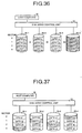
In a RAID5 disk array device, a disk device for parity
is not fixed, so that operations for data read and data write
can concurrently be executed. Namely, as shown in Fig. 37,
parities for sectors are written in different disk devices
respectively. Herein parity P1 is computed from data a1, b1,
c1, parity P2 from data a2, b2, d2, parity P3 from data a3, c3,
d3, and parity P4 from data b4, c4, d4.
-
As for concurrent operations for data read and data write,
for instance, data a1 for sector 0 of the disk device 32-1 and
data b2 for sector 1 of the disk device 32-2 are placed in the
disk devices 32-4 and 32-3 having parity P1 and parity P2
different from each other respectively, so that the operations
for reading data and writing data can concurrently be executed.
It should be noted that overhead required for accessing 4 times
in all is the same as that in RAID4.
-
As described above, in a case of RAID5, operations for
data read and data write can concurrently be executed by
accessing a plurality of disk devices asynchronously, so that
this type of disk array device is suited to transaction
processing executed by accessing a small volume of data at
random.
-
In the conventional types of disk array devices as
described above, when power supply is interrupted for some
reasons while data write to a disk device is being executed,
the system control can be started from the same operation for
writing data after recovery of power supply in RAID1 to RAID3
disk array devices, but the same write operation can not be
restarted after recovery of power supply in RAID4 and RAID5 disk
array devices for the following reasons.
-
When writing data in a RAID4 or a RAID 5 disk array device,
a parity is decided by computing exclusive-OR (expressed by the
exclusive-OR symbol) for data in a plurality of disk devices
through the equation (1) below and the parity is stored in a
disk device for parity.
Data a (+) data b (+) · · · = Parity P
-
Sites for storage of data and parity are fixed, in a case
of RAID4, to particular disks 32-1 to 32-4 as shown in Fig. 36.
In contrast, in a case of RAID5, sites for storage of parity
are distributed to the disk devices 32-1 to 32-4 as shown in
Fig. 37 to dissolve concentration of access to a particular disk
or particular disks due to operations for reading and writing
parity.
-
When reading data from these RAID4 and RAID5 types of disk
array devices, data in the disk devices 32-1 to 32-4 cannot be
rewritten, so that consistency of parity is maintained, but also
parity must be rewritten according to data when writing data
therein.
-
For instance, when old data (a1) old in the disk device
32-1 is rewritten to new data (a1) new, parity P1 for all the
data in the disk device can be maintained by updating parity
by computing through the equation (2):
Old data (+) old parity (+) new data = New parity
-
As shown by this equation (2), it is necessary to read
out old data and old parity in the disk device first, and then
an operation for writing new data and operations for generating
and writing new parity are executed.
-
Next detailed description is made for a method of
rewriting data in a RAID5 type of disk array device with
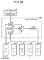
reference to Fig. 38. Fig. 38 is a simulated view for
illustrating a sequence for rewriting data, and in this figure,
an array controller 50 is connected to 5 units of disk devices
( Devices 0, 1, 2, 3, 4) 32-1, 32-2, 32-3, 32-4, and 32-5 for
the purpose to control the disk devices 32-1 to 32-5, and a host
computer 18 is connected to the array controller 50 via a control
unit 10 for controlling the array controller 50.
-
For instance, when rewriting data (D0) in the disk device
32-1, at first the control unit 10 issues a write command to
the array controller 50, and also transfers write data (D0 new)
40 to the array controller 50. The array controller 50 receives
the write command from the control unit 10, and reads out old
data (D0 old) 40-1 from the disk controller 32-1. Also the array
controller 50 reads out old parity (Dp old) from the disk device
32-5.
-
Then the array controller 50 writes the new data (D0 new)
in the disk device 32-1. Then the array controller 50 computes
exclusive-OR (EOR) with a logic circuit 12 among old parity (DP
old) 48, old data (D0 old) 40-1, and new data (D0 new) 40 to
generate new parity (Dp new) 48-1, and write the new parity in
the disk device 32-5. Then the array controller 50 reports to
the control unit 10 that the write operation has been finished
normally, and the control unit 10 acknowledges the report, thus
data updating being finished.
-
If power is cut off while writing new data or new parity
in a RAID4 or a RAID5 type of disk array device, it becomes
impossible to check up to where data has been written normally,
and consistency of parity is lost. If the processing for writing
the same data is executed after recovery of power, old data and
old parity are read from a disk device or disk devices with
consistency of parity having been lost therefrom, so that
inconsistent parity is generated and the data write operation
is disadvantageously finished.
-
To solve the problem described above, the present
inventors proposed RAID4 and RAID5 types of disk array device
in which, even if power is cut off during an operation for writing
new data or new parity, the interrupted operation for writing
the same data or same parity can be restarted (Refer to Japanese
Patent Laid-Open Publication No. HEI 6-119126). The disk array
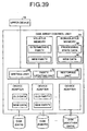
device according to this invention is shown in Fig. 39.
-
In this disk array device, at least processing state data
38 indicating a processing state of a writing unit 60 as well
as of a parity updating unit 70 and new data 40 transferred from
an upper device 18 are stored in an nonvolatile memory 34 in
preparation for a case where power goes down, and when power
is turned ON, a restoring unit 80 executes the processing for
recovery using the new data 40 maintained in the nonvolatile
memory 34 with reference to the processing state data 38 in the
nonvolatile memory 34 when the write processing has been
interrupted.
-
However, out subsequent study showed that, in the
invention disclosed in Japanese Patent Laid-Open Publication
No. HEI 6-119126, if any one of a plurality of disk devices goes
wrong, sometimes the processing for recovery can not be executed.
Namely, in the configuration shown in Fig. 38, for instance,
if the disk device 32-2 is faulty, when power is cut off and
the operation for writing data is interrupted while rewriting
new data (D0) new) or new parity (Dp new), not only data (D0)
in the disk device 32-1 and parity (Dp) in the disk device 32-5
are broken, but also it becomes impossible to reconstruct data
(D1) during data stripe and constituting the same parity group
in the faulty disk device 32-2, thus the data being lost.
-
Also it is conceivable that the invention disclosed in
Japanese Patent Laid-Open Publication No. HEI 6-119126 is
applied to a RAID5 disk array device having a plurality of array
controllers. Namely, an nonvolatile memory is provided in a
disk array device having a plurality of array controller, new
data and processing state data are stored in the nonvolatile
memory, and the processing for data recovery is executed, when
the data write processing is not finished normally due to power
failure or for any other reason, using the data.
-
However, when a plurality of array controllers are booted
up with independent power supply units respectively, time delay
is generated. For this reason, if power supply is restarted
after processing for writing data has not been normally finished
in a plurality of array controllers, the processing for recovery
is executed to data in a parity group updated immediately after
data recovery by an array controller using data stored in an
nonvolatile memory in another array controller, and the last
data is disadvantageously lost.
SUMMARY OF THE INVENTION
-
It is an object of the present invention to provide a disk
array device which can restart, even if power goes down during
data write processing, the interrupted data write processing
after recovery of power to complete the processing, especially
a disk array device in which data can be restored even if any
of a plurality of disk devices is faulty, or a disk array device
having a plurality of array controllers in which data can be
restored.
-
Fig. 1 is an explanatory view showing an operational
principle of a disk array device according to the present
invention. As shown in Fig. 1, the disk array device belongs
to the category of RAID4 or RAID5, and comprises a control unit
10, an array controller 50, and a plurality unit (for instance,
5 units in Fig. 1) of disk devices 32-1, 32-2, 32-3, 32-4, and
32-5.
-
Provided in the control unit 10 are a channel interface
adapter 16, an nonvolatile memory 34, a special write executing
unit 110, and a data reproducing means 120. An upper device
18 such as a host computer is connected via the channel interface
adapter 16 to the disk array device. The nonvolatile memory 34
stores therein new data transferred from the upper device.
-
When the write processing is interrupted once and then
restarted, if regeneration of parity is impossible because new
data is stored in the nonvolatile memory 34 and data can not
is read out normally from a third disk device (for instance,
32-2) excluding a disk device (for instance, 32-1), to which
it has been instructed for new data to be written in, and a disk
device for parity (for instance, 32-5), the special write
executing unit 110 executes the processing for restoring data
by generating new parity using new data stored in the
nonvolatile memory 34, and writes the new data, new parity and
other data in the disk device by means of special write
processing.
-
Namely, the special write executing unit 110 has a data
write unit 113 and a parity generating unit 116, and the data
write unit 113 overwrites a preset special value or preferably
new data stored in the nonvolatile memory 34, when executing
the special write processing, at a specified write position in
the specified disk device (for instance, 32-1).
-
Also when executing the special write processing, the
parity generating unit 116 generates new parity using data and
parity stored at positions corresponding to disk write
positions for new data in a disk device (for instance, 32-1),
to which it has been instructed for new data to be written in,
and a disk device for parity (for instance, 32-5) and also using
new data stored in the nonvolatile memory 34, and writes the
new parity in the disk device for parity (for instance, 32-5).
-
The data reproducing unit 120 issues a request for shift
to the special write processing mode to the special write
executing unit 110 when there is a third disk device (for
instance, 32-2) from which data can not be read out normally
in processing for recovery).
-
Provided in the array controller 50 are a plurality (for
instance, 5 units in Fig. 1) of device interface adapters 54-1,
54-2, 54-3, 54-4, and 54-5. Data error detecting units 154-1,
154-2, 154-3, 154-4, 154-5 are provided in the device interface
adapters 54-1, 54-2, 54-3, 54-4, and 54-5, respectively. The
data error detecting units 154-1, 154-2, 154-3, 154-4, 154-5
detects generation of an error when reading out data from the
disk devices 32-1, 32-2, 32-3, 32-4, and 32-5, and reports
generation of the error to the data reproducing unit 120.
-
In a disk array device having the configuration described
above, the processing for data recovery is executed as described
below. After processing for writing new data is interrupted
due to power failure or for other reasons, when the write
processing is restarted because power supply is restarted or
for other reasons, at first parity stored at a position
corresponding to a disk write position for new data in a disk
device for parity (for instance, 32-5) is read out. In this
step, a read error is detected by the data error detecting unit
(for instance, 154-5) because consistency of parity with that
of data has been lost due to interruption of the previous write
processing.
-
Then the data error detecting unit (for instance, 154-5)
reports generation of an error to the data reproducing unit 120.
When the data reproducing unit 120 receives the report, it reads
out data, for reproducing the parity data, from disk devices
(for instance, 32-2, 32-3, 32-4) other than a disk device as
a target for new data write (for instance, 32-1) and a disk device
for parity (for instance, 32-5) each belonging to the parity
group in which the read error was generated.
-
In this step, if a further read error is detected by the
data error detecting unit (for instance, 154-2) while reading
out data from a third disk device (for instance, 32-2), the data
error detecting unit reports generation of the error to the data
reproducing unit 120. With this operation, the data
reproducing unit 120 issues a request for shift to the special
write processing mode to the special write executing unit 110.
-
When the special write executing unit 110 receives a
request for shift to the special write processing mode, the data
write unit 113 overwrites a preset special value or preferably
new data stored in the nonvolatile memory 34 at specified write
positions in the specified disk device (for instance, 32-1).
-
The parity generating unit 116 generates new parity using
data and parity stored at positions corresponding to specified
write positions in a disk device (for instance, 32-1), to which
it has been instructed for new data to be written in, as well
as in a disk device for parity (for instance, 32-5), and writes
the new parity in the disk device for parity (for instance, 32-5).
Then the special write processing mode is terminated.
-
It should be noted that, when a preset special value is
overwritten at a specified write position in a specified disk
device (for instance, 32-1) (for instance, when new data is not
stored in the nonvolatile memory 34), the data write unit 113
memorizes that the special value was overwritten, for instance,
by providing a flag in the memory, and simulatedly reports a
read error when a read request is issued to the data.
-
As described above, a disk array device according to the
present invention is a disk array device adapted to data
updating by reading out old data stored at a write position of
a specified disk device, then writing new data transferred from
a upper device at the write position, and writing a new parity
generated according to an old parity stored at a disk write
position for the new data on a disk device for parity, the old
data as well as to the new data at a disk storage position for
the old parity, comprising an nonvolatile memory for storing
therein new data transferred from a upper device; and a special
write executing unit for executing processing for recovery, in
a case where, when write processing is interrupted once and then
the interrupted write processing is restarted, it is impossible
to restore a parity because required data can not normally be
read out from a third disk device other than a first disk device
in which the new data is stored in the nonvolatile memory thereof
and also in which new data is to be written and a second disk
for parity, by generating a new parity by means of using data
and parity stored at a position corresponding to a disk write
position for the new data on the first disk device and the second
disk device and new data stored in the nonvolatile memory.
-
With the disk array device according to the present
invention, when write processing interrupted once due to power
failure or for other reason is restarted, processing for
recovery of data is executed, even when there is any faulty disk,
by generating new parity (Dp new) using data (D0 old, Dp old)
stored at positions corresponding to disk write positions for
new data (D0 new) in the disk device, to which it has been
instructed for new data (D0 new) to be written in as well as
in the disk device for parity and new data (D0 new) stored in
the nonvolatile memory.
-
A disk array device according to the present invention
characterized in that the data stored at positions
corresponding to disk write positions for the new data on all
disk devices other than the first disk device, second disk
device, and third disk device, and the generated new parity are
stored in the nonvolatile memory, and the special write
executing unit concurrently writes the new data stored in the
nonvolatile memory, the data stored at corresponding positions
of all disk devices excluding the first disk device, second disk
device, and third disk device, and the generated new parity in
corresponding disks.
-
With the disk array device according to the present
invention, when restarting the write processing once
interrupted, new data (D0 new), other data (D2, D3), and new
parity (Dp new) are concurrently written into corresponding
disk devices, so that the processing for recovery of data can
be executed even if there is any faulty disk.
-
A disk array device according to the present invention
is characterized in that, a write flag indicating that write
processing is being executed and management information
indicating progression of the write processing are stored in
the nonvolatile memory in a period of time from a time when a
write processing instruction is received from an upper device
until the write operation is finished in the normal state.
-
With the disk array device according to the present
invention, as a write flag indicating whether an operation for
writing data into a disk device has been finished normally or
not and a status indicating a stage of the write processing are
stored in an nonvolatile memory, if the write processing has
not been finished normally, when power supply is restarted,
whether any data not having been written in the normal state
is remaining or not can visually and easily be checked by
referring to the write flag, and also the recovery processing
can be restarted from the point where the write processing was
interrupted by referring to the status, so that the recovery
processing can rapidly be executed.
-
A disk array device according to the present invention
is a disk array device comprising a plurality of array
controllers each driven by an independent power supply unit for
writing and reading data and parity to and from a plurality of
disk device, and a control unit for controlling the array
controller, and executing data updating by reading out old data
stored at a write position on a specified disk device, then
writing new data transferred from an upper device at the write
position, and further writing a new parity generated according
to an old parity, old data, and new data read from storage
positions corresponding to disk write positions for the new data
in a disk device for parity at disk storage positions for the
old parity; wherein the control unit comprises a nonvolatile
memory for storing therein at least the new data, old data, and
old parity, when write processing is instructed from an upper
device, before the write processing is executed to a disk
device; a task generating unit for generating, when it is
reported that an array controller, to which power supply has
been stopped, is included in the plurality of array controllers,
a task for allocating the write processing being executed by
the array controller with power supply having been stopped
thereto or write processing to be executed by the array
controller but not having been completed to other array
controllers; and a task information table for storing therein
the task generated by the task generating unit; and further the
plurality of array controllers each comprise a power monitoring
unit for mutually monitoring the power supply state; a power
supply stop reporting unit for reporting to the control unit
the fact that stoppage of power supply to other array controller
or controllers has been detected; and a parity generating unit
for generating a new parity according to data read from a storage
position corresponding to a disk write position for the new data
on all disks excluding the disk device in which it has been
specified to write new data and the disk device for parity as
well as to new data transferred from the nonvolatile memory.
-
With the disk array device according to the present
invention, when a write instruction is issued from an upper
device, new data (D0 new), old data (D0 old), and old parity
(Dp old) are stored in a non volatile memory prior to execution
of the write processing to a disk device, so that, when a trouble
is generated in the write processing by one of array controllers,
another array controller can continue the write processing in
stead of the faulty array controller, and for this reason
consistency of data is maintained.
-
A disk array device according to the present invention
is characterized in that, management information indicating
progression of write processing is stored in the nonvolatile
memory, and the task generating unit generates a task according
to the management information stored in the nonvolatile memory.
-
With the disk array device according to the present
invention, a status indicating a stage of the write processing
and an ID flag indicating an array controller having executed
the process indicated by the status are stored in a nonvolatile
memory, and a task for alternative processing is generated
according to the status, so that the write processing can be
restarted from the interrupted point.
-
A disk array device according to the present invention
is a disk array device comprising a plurality of array
controllers each driven by an independent power supply unit for
writing and read data and parity to and from a plurality of disk
device, and a control unit for controlling the array controller,
and executing data updating by reading out old data stored at
a write position on a specified disk device, then writing new
data transferred from an upper device at the write position,
and further writing a new parity generated according to an old
parity, old data, and new data read from storage positions
corresponding to disk write positions for the new data in a disk
device for parity at disk storage positions for the old parity;
wherein each of the plurality of array controllers comprises
a nonvolatile memory for storing, when write processing is
instructed from an upper device, and before the write processing
to a disk device is executed, at least the new data, old data,
and old parity therein; and a communicating unit for executing
transaction of data and parity with another array controller,
transmitting, when the new data, old data, and old parity have
been stored in the nonvolatile memory in one of the array
controllers, the new data, old data, and old parity stored in
the nonvolatile memory from the one array controller to the
other array controller before write processing is executing to
a disk device, and also receiving the new data, old data, and
old parity sent from the one array controller to the other array
controller and storing them in the nonvolatile memory of the
other array controller.
-
With the disk array device according to the present
invention, when an instruction for write processing is issued
from an upper device, new data (D0 new), old data (D0 old), new
parity (Dp old) or new parity (Dp new) are stored in the
nonvolatile memory of one of the array controllers before
execution of the write processing to a disk device, and further
new data (D0 new), old data (D0 old), and old parity (Dp old)
are copied into a nonvolatile memory of another array controller,
so that, even if the processing for writing data and parity is
not finished in the normal status due to power failure or for
some other reasons, when power supply is restarted, the recovery
processing can easily be executed by using new data (D0 new)
stored in a nonvolatile memory in one of the array controllers
or in the other one.
-
A disk array device according to the present invention
is characterized in that, management information indicating
progression of write processing is stored in the nonvolatile
memory.
-
With the disk array device according to the present
invention, a status indicating a stage of write processing is
stored in the nonvolatile, so that, after the write processing
is not finished in the normal state, when power supply is
restarted, the write processing can be restarted from the
interrupted point by referring to the status.
-
A disk array device according to the present invention
is characterized in that, when write processing is interrupted
in the one of the array controllers and then the array controller
interrupted as described above is restored to a stable allowing
the normal operation, the one of the array controllers, or the
other array controller having received the new data, old data,
and old parity from the one of the array controller before
interruption of the write processing executes the interrupted
write processing again according to the new data, old data, and
old parity stored in a respective nonvolatile memory.
-
With the disk array device according to the present
invention, write processing once interrupted is restarted
according to new data (D0 new), old data (D0 old), and old parity
(Dp old) stored in a nonvolatile memory, so that the recovery
processing can easily be executed.
-
A disk array device according to the present invention
is a disk array device comprising a plurality units of disk
devices, and an array controller for writing and reading data
and parity to and from the disk devices and adapted for data
updating by reading old data stored at a write position of a
specified disk device and then writing new data transferred from
an upper device at the write position, and also writing a new
parity generated according to an old parity, old data, and new
data read from a storage position corresponding to a disk write
position for the new data on a disk device for parity at a disk
storage position for the old parity; characterized in that the
disk array device further comprises a non-failure power supply
unit for baking up power supply to the plurality units of disk
device as well as power supply to the array controller.
-
With the disk array device according to the present
invention, even when AC input to a power supply unit is stopped,
or when power supply between a power supply unit and an array
controller or that between a power supply unit and a disk device
is down for some reasons or other, power supply is executed
continuously, so that the write processing by an array
controller is not interrupted with consistency of data
maintained.
-
A disk array device according to the present invention
is a disk array device adapted for data updating by reading out
old data stored at a write position of a specified disk device
and then new data transferred from an upper device at the write
position, and also writing a new parity generated according to
an old parity, old data, and new data stored at a write position
corresponding to the disk write position for the new data on
a disk device for parity at the disk storage position for the
old parity; and the disk array device further comprises a
special write executing unit for executing processing recovery,
when, of a data group as a basis for a parity, data in at least
two disk units can not be read out normally, by writing arbitrary
data in the two disk devices from which data can not be read
out normally and generating a new parity using the data
arbitrarily written and data normally read out from the data
group as a basis for a parity; and a data error detecting unit
for issuing a data check response to read to the data arbitrarily
written by the special write executing unit.
-
With the disk array device according to the present
invention, although data written in a disk device, from which
data can normally be read out, can not be reproduced, by
generating new parity by means of writing arbitrary data in the
disk device, the disk device can normally be operated according
to a write instruction from an upper device. For this reason,
the recovery processing from an upper device can be executed.
-
Also with the disk array device according to the present
invention, by memorizing that arbitrary data has been written
at a place where unreadable data is stored in a disk device from
which data can not normally be read out, and also by sending
an error or the like in response to a read instruction from an
upper device for the written arbitrary data, it is possible to
prevent the arbitrary data from erroneously be sent to the upper
device.
-
Other objects and features of this invention will become
understood from the following description with reference to the
accompanying drawings.
BRIEF DESCRIPTION OF THE DRAWINGS
-
- Fig. 1 is an explanatory view for illustrating principles
of a disk array device according to the present invention;
- Fig. 2 is a block diagram showing Embodiment 1 of the disk
array device according to the present invention;
- Fig. 3 is a functional block diagram showing a case where
one of the disk devices in Embodiment 1 of the disk array device
according to the present invention is faulty;
- Fig. 4 is a functional block diagram showing a case where
no disk device in Embodiment 1 of the disk array device according
to the present invention is faulty;
- Fig. 5 is a simulated view showing an example of contents
stored in a management table stored in a nonvolatile memory in
Embodiment 1;
- Fig. 6 is a flow chart showing a general flow of operations
in Embodiment 1 of the disk array device according to the present
invention;
- Fig. 7 is a flow chart showing details of the processing
for writing data as well as for updating parity in Embodiment
1 of the disk array device according to the present invention;
- Fig. 8 is a flow chart showing details of special data
write processing in Embodiment 1 of the disk array device
according to the present invention;
- Fig. 9 is a flow chart showing details of ordinary data
write processing in Embodiment 1 of the disk array device
according to the present invention;
- Fig. 10 is a flow chart showing details of recovery
processing in Embodiment 1 of the present invention;
- Fig. 11 is a flow chart showing details of recovery
processing in NFT in Embodiment 1 of the disk array device
according to the present invention;
- Fig. 12 is a flow chart sowing details of recovery
processing in FT in Embodiment 1 of the disk array device
according to the present invention;
- Fig. 13 is a flow chart showing details f the data read-out
processing in Embodiment 1 of the disk array device according
to the present invention;
- Fig. 14 is a block diagram showing Embodiment 2 of the
disk array device according to the present invention;
- Fig. 15 is a functional block diagram showing a case where
one of disk devices in Embodiment 2 of the disk array device
according to the present invention;
- Fig. 16 is a functional block diagram showing a case where
there is no faulty disk device in Embodiment 2 of the disk array
device according to the present invention;
- Fig. 17 is a block diagram showing Embodiment 3 of the
disk array device according to the present invention;
- Fig. 18 is a functional block diagram showing Embodiment
3 of the disk array device according to the present invention;
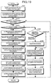
- Fig. 19 is a flow chart showing details of write
processing in Embodiment 3 of the disk array device according
to the present invention;
- Fig. 20 is a flow chart showing details of the processing
in response to a write instruction to other disk device issued
before generation of abnormality to an array controller in which
abnormality has been generated in Embodiment 3 of the disk array
device according to the present invention;
- Fig. 21 is a functional block diagram showing Embodiment
4 of the disk array device according to the present invention;
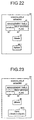
- Fig. 22 is a simulated view showing a case in which a
management table, new data, and new parity are stored in a
nonvolatile memory in Embodiment 4;
- Fig. 23 is a simulated view showing a case in which a
management table, new data, and intermediate parity are stored
in a nonvolatile memory in Embodiment 4;
- Fig. 24 is a flow chart showing details of write
processing in Embodiment 4 of the disk array device according
to the present invention;
- Fig. 25 is a flow chart showing details of recovery
processing in Embodiment 4 of the disk array device according
to the present invention;
- Fig. 26 is a functional block diagram showing Embodiment
5 of the disk array device according to the present invention;
- Fig. 27 is a simulated view showing an example of contents
of a management table stored in a nonvolatile memory in
Embodiment 2;
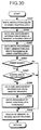
- Fig. 28 is a flow chart showing details of write
processing in Embodiment 5 of the disk array device according
to the present invention;
- Fig. 29 is a functional block diagram showing a variant
of Embodiment 5 of the disk array device according to the present
invention;
- Fig. 30 is a flow chart showing details of write
processing in the variant;
- Fig. 31 is a functional block diagram showing Embodiment
6 of the disk array device according to the present invention;
- Fig. 32 is an explanatory view showing a disk array device
according to RAID0;
- Fig. 33 is an explanatory view showing a disk array device
according to RAID1;
- Fig. 34 is an explanatory view showing the disk array
device according to RAID3;
- Fig. 35 is an explanatory view showing data division
according to RAID3;
- Fig. 36 is an explanatory view showing a disk array device
according to RAID4;
- Fig. 37 is an explanatory view showing the disk array
device according to RAID5;
- Fig. 38 is an explanatory view showing a sequence for
rewriting data according to RAID5; and
- Fig. 39 is a functional block diagram of a disk array
device according to a previous invention applied by the present
inventors.
-
DESCRIPTION OF THE PREFERRED EMBODIMENT
-
Next detailed description is made for embodiments of the
disk array device according to the present invention with
reference to Fig. 2 to Fig. 31.
-
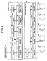
Fig. 2 is a block diagram showing Embodiment 1 of a disk
array device according to the present invention. In Fig. 2,
provided in a control unit 10 is a microprocessor (described
as MPU hereinafter) 12. Connected to an internal bus of this
MPU 12 are a ROM 20 in which control program or specified data
is stored, a volatile memory 22 using a RAM, a cache memory 26
provided via a cache function engine 24, a nonvolatile memory
34 operable even during power failure because of a backup power
supply unit 36, a resource manager module 13 managing internal
resources or internal jobs, and an service adapter 14 for
managing the hardware environment.
-
Also a channel interface adapter 16 is provided in the
control unit 10, and a host computer 18 functioning as an upper
device is connected via the adapter 16 to the control unit 10.
Further, a device interface adapter 17 is provided in the
control unit 10, and an array controller 50 controlling a
plurality units (for instance, 5 units in Fig. 2) of disk devices
32-1, 32-2, 32-3, 32-4, and 32-5 is connected via the adapter
17 to the control unit 10.
-
Provided in the array controller 50 are an upper interface
52 connected to the device interface adapter 17 in the control
unit 10, and a plurality units (for instance,5 units in Fig.
2) of device interface adapters 54-1, 54-2, 54-3, 54-4, and 54-5
as functioning as lower interfaces with a plurality units of
disk devices 32-1 to 32-5 connected thereto.
-
Of the 5 units of disk devices 32-1 to 32-5, for instance,
4 units of the disk devices are used for storage of data, and
one unit of the devices is used for parity. In the disk array
device according to the present invention, the same function
as that in the RAID4 type of disk array device shown in Fig.
36 or in the RAID5 type of disk array device shown in Fig. 37
is realized, so that, in a case of the RAID4 type of disk array
device, for instance, disk devices 32-1 to 32-4 are used for
storage of data, while the disk device 32-5 is used for parity.
On the other hand, in a case of the RAID5 type of disk array
device, like in a case of the RAID4 type of disk devices, any
of the disk devices 32-1 to 32-5 is not used dedicatedly for
parity although one disk device stores therein data having the
same format in batch, and the disk devices are successively used
as a disk device for storage of parity according to a
prespecified sequence in response to a sector.
-
Fig. 3 and Fig. 4 are functional block diagrams each
showing the disk array device according to Embodiment 2, and
Fig. 3 shows a case where one of the disk units is faulty, and
Fig. 4 shows a case where no device is faulty, namely where all
the disk devices are normally working.
-
Fig. 3 and Fig. 4 assume a case where, of a plurality unit
(5 units in Fig.3 and Fig. 4) of the disk devices 32-1 to 32-5,
for instance, a disk device 32-5 is used as a disk device for
parity. It is needless to say that, if the disk device 32-5
is of the RAID4 type, the disk device is used only for storage
of parity, and in a case of the RAID5, the disk device is used
for storage of parity in current data access.
-
When updating data (D0) in the specified disk device 32-1
to new data (D0 new) while one disk device 32-2 is faulty, as
shown in Fig. 3, stored in a nonvolatile memory 34 in the control
unit 10 are new data (D0 new) transferred from the host computer
18, a management table 41 showing progression of the write
processing or the like, a write flag 44 indicating that an
operation for writing is being executed, old data (D0 old) 40-1
read out from the disk device 32-1, data (D2, D3) 46, 47 read
out from the normal disk devices 54-3 and 54-4, old parity (Dp
old) 48 read out from the disk device for parity 32-5, and new
parity (Dp new) 48-1 computed through exclusive-OR (EOR) among
old data (D0 old) 40-1, new data (D0 new) 40, and old parity
(Dp old) 48.
-
The processing for generating new parity (Dp new) 48-1
is executed in a parity generating unit 116 (Refer to Fig.
1) in the special write executing unit 110. It should be noted
that the special write executing unit 110 is realized with the
MPU 12 shown in Fig. 2.
-
To prevent generation of data loss, the special data write
processing is executed. Namely, the new data (Do new) 40 stored
in the nonvolatile memory 34 , other data (D2, D3) 46, 47, and
new party (Dp new) 48-1 are sent to and stored in device interface
adapters 54-1, 54-3, 54-4, 54-5 in the array controller 50.
-
The new data (0 new) 40-2, other data (D2, D3) 46-1, 47-1,
and new parity (Dp new) 48-2 stored in the device interface
adapters 54-1, 54-3, 54-4, 54-5 are concurrently written in the
disk devices 32-1, 32-3, 32-4, 32-5 according to the RAID3
system. The processing for overwriting the new data (D0 new)
in the disk device 32-1, to which the write processing is
specified, is executed by the data write unit 113 in the special
write executing unit 110.
-
A stage (status) of the write processing 42 and a
self-system flag 43 indicating, when a plurality of array
controllers are provided, whether the write processing is being
executed by the system or by any other system are stored in the
management table 41.
-
Computing for exclusive-OR is executed, for instance,
by the MPU 12.
-
When the write processing not having been finished in the
normal state is to be restored, the new data (Do new) 40, other
data (D2, D3) 46, 47, and new parity (Dp new) stored in the
nonvolatile memory 34 are concurrently written via the device
interface adapters 54-1, 54-3, 54-4, 54-5 of the array
controller 50 in the disk devices 32-1, 32-3, 32-4, and 32-5
according to the RAID3 system.
-
When data (D0) in the specified disk device 32-1 is to
be updated to new data (Do new) in the state where all the disk
devices 32-1, 32-2, 32-3, 32-4, 32-5 are operating, as shown
in Fig. 4, the new data (D0 new) 40 transferred from the host
computer 18, management table 41 showing a status of the write
processing, and write flag 44 indicating that the write
processing is being executed are stored in the nonvolatile
memory 34 of the control unit 10.
-
Also stored in the nonvolatile memory 22 of the control
unit 10 are old data (D0 old) 40-1 read out from the disk device
32-1 and old parity (Dp old) read out from the disk device for
parity 32-5.
-
In this case, the ordinary write processing is executed.
Namely, the new data (D0 new) stored in the nonvolatile memory
34 is sent to and stored in the device interface adapter 54-1
of the array controller 50, and the stored new data (D0 new)
40-2 are written in the disk device 32-1.
-
Computing for exclusive-OR (EOR) is executed in the MPU
12 depending on the new data (D0 new) 40 stored in the nonvolatile
memory 34 and old data (D0 old) stored in the nonvolatile memory
22, and old parity (Dp old) 48 also stored in the nonvolatile
memory 22 to obtain new parity (Dp new) 48-1, and the new parity
(Dp new) 48-1 is stored in the nonvolatile memory 22 in the
control unit 10. This new parity (Dp new) 48-1 is stored in
the device interface adapter 54-5 of the array controller 50,
and the stored new parity (Dp new) 48-2 is written in the disk
device 32-5.
-
When write processing not having been finished in the
normal state is to be restored, the new data (Do new) stored
in the nonvolatile memory 34 is written via the device
interface adapter 54-1 of the array controller 50 in the disk
device 32-1. Also because the write processing was not finished
in the normal state, old data (D0 old) and old parity (Dp old)
have not been fixed yet, and for this reason data (D1, D2, D3)
is read out from the disk devices 32-2, 32-3, 32-4 to generate
new parity (Dp new) and are stored in the device interface
adapters 54-2, 54-3, and 54-5.
-
The data (D1, D2, D3 ) 45-1, 46-1, 47-1 stored as described
above are sent to and stored in the nonvolatile memory 22 in
the control unit 10. And, new parity (Dp new) 48-1 is obtained
from the data (D1, D2, D3) 45, 46, 47 stored in the nonvolatile
memory 22 and new data (Do new) stored in the nonvolatile memory
34, and is written via the device interface adapter 54-5 of the
array controller 50 in the disk device 32-5.
-
Fig. 5 shows an example of contents stored in the
management table 41, which is stored in the nonvolatile memory
34. As shown in the figure, the items of "op-id", "status"
corresponding to the status 42 in Fig. 3 and Fig. 4, "self
system/other system" corresponding to the self-system flag 43
in Fig. 3 and Fig. 4, and "address" are stored in the management
table 41.
-
The "op-id" is an ID for controlling write processing by
the array controller 50; "status" indicates to which state the
write processing has progressed; "self system/other system"
indicates, where there are provided a plurality of array
controllers, whether the controller having executed the
processing shown in the status is in the system or in other
system; and "address" indicates a site for storage of data or
parity stored in the nonvolatile memory 34.
-
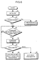
Fig. 6 is a flow chart showing the entire operating
sequence in the disk array device shown in Fig. 3 and Fig. 4.
In Fig. 6, when power for the disk array device is turned ON,
a prespecified operation for initialization is executed
according to the initial program routine (IPL) in step S1, and
then checking as to whether power down has occurred or not is
executed in step S2. When system control is started upon
logging-on after the power is turned OFF by means of an ordinary
operation for logging off, it is determined that power down has
not occurred with the system control shifted to step S3, and
reception of a command from the host computer 18 is waited.
-
When a command is received from the host computer 18 in
step S3, system control shifts to step S4, where the command
is decoded. When a demand for write access is detected in step
S5, system control shifts to step S6 to execute data write and
parity updating, and on the other hand when a demand for read
access is detected in step S5, system control shifts to step
S7 to execute data read.
-
On the other hand, when system control is started upon
power ON, if it is determined in step S2 that power down has
occurred, the processing for recovery is executed in step S8,
and then the ordinary operating sequence from step S3 and on
is executed. The program for executing this operating sequence
is stored in a ROM 20 (Refer to Fig. 2) in the control unit 10,
and the program is executed by the MPU 12 (Refer to Fig. 2).
-
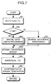
Fig. 7 is a flow chart showing details of the data write
processing and parity updating shown in step S6 in Fig. 6. In
Fig. 7, when a write command is received from the host computer
18, at first the write flag 44 is prepared in step S61 in the
nonvolatile memory 34 in the control unit 10. Then system
control shifts to step S62, and an operating state of all the
disk devices 32-1, 32-2, 32-3, 32-4, and 32-5 is checked.
-
When there is any faulty disk (for instance, the disk
device 32-2 in Fig. 3) (NFT), system control shifts to step S63
to execute the special data write processing, and if all the
disk devices 32-1, 32-2, 32-3, 32-4, 32-5 are operating (FT),
system control shifts to step S67 to execute the ordinary data
write processing.
-
When data write is finished in step S63 or step S67, the
controller 10 receives in step S64 a report indicating that the
write processing was finished in the normal state from the array
controller 50 with the write flag 44 deleted in step S65, and
it is confirmed in step S66 that the write processing was
finished. With this operation, the processing for writing data
and updating parity is complete.
-
Fig. 8 is a flow chart showing details of the special data
write processing shown in step S63 in Fig. 7. It should be noted
that contents of the processing shown in Fig. 8 is the same as
those in the functional block diagram in Fig. 3. In Fig. 8,
new data to be written in the disk device is transferred from
the host computer 18 in association with the write command, so
that new data (D0 new) from the host computer 18 is stored in
the nonvolatile memory 34 in the control unit 10 in step S631.
-
Then in step S632, old data (D0 old) 40-3, other data (D2,
D3) 46-1, 47-1, and old parity (Dp old) 48-3 are read out from
all the disk devices 32-1, 32-3, 32-4, 32-5 excluding a faulty
disk device (Disk device 32-2 in Fig. 3) according to
instructions from the device interface adapters 54-1, 54-3,
54-4, and 54-5 and are stored in the device interface adapters
54-1, 54-3, 54-4, and 54-5. The stored old data (D0 old) 40-3,
other data (D2, D3) 46-1, 47-1, and old parity (Dp old) 48-3
are transferred in step S633 to the control unit 10 and stored
in the nonvolatile memory 34.
-
Then system control shifts to step S634, and new parity
(Dp new) 48-1 is generated from exclusive-OR among the old data
(D0 old), old parity (Dp old) 48, and new data (D0 new) 40 each
stored in the nonvolatile memory, and the new parity is stored
in step S635 in the nonvolatile memory 34.
-
Then system control shifts to step S636; the new data
(D0 new) 40 and other data (D2, D3) 46, 47, and new parity (Dp
new) 48-1 each stored in the nonvolatile memory 34 are
transferred and stored in the device interface adapters 54-1,
54-3, 54-4, 54-5; in step S637 new data (D0 new) 40-2, other
data (D2, D3) 46-1, 47-1, and new parity (Dp new) 48-2 are
transferred to the disk devices 32-1, 32-3, 32-4, 32-5; in step
S638 new data (D0 new) 40-2, other data (D2, D3) 46-1, 47-1,
and new parity (Dp new) 48-2 are concurrently written in the
same regions as those for new data to be written in of the disk
devices 32-1, 32-3, 32-4, and 32-5. With this operation, the
special data write processing is finished.
-
Fig. 9 is a flow chart showing details of the ordinary
data write processing shown in step S67 in Fig. 7. It should
be noted that contents of the processing shown in Fig. 9 is the
same as those shown in the functional block diagram in Fig. 4.
In Fig. 9, at first, in step S671, the new data (D0 new) 40
transferred from the host computer 18 in association with a
write command is stored in the nonvolatile memory 34 of the
control unit 10. Then in step S672, if the disk device 32-1
is specified as a disk device for data write, the new data
(D0 new) is transferred to and stored in the device interface
adapter 54-1.
-
Then in step S673, according to an instruction from the
device interface adapter 54-1, contents of a region, in which
the new data is to be written, of the disk device 32-1 is read
as old data (D0 old) 40-3 and is stored in step S674 in the device
interface adapter 54-1.
-
When the old data (D0 old) 40-3 has been stored, in step
S675, new data (D0 new) in the device interface adapter 54-1
is transferred to the disk device 32-1, and in step S676, the
new data (D0 new) 40-2 is written in the region in which the
new data is to be written.
-
Then, contents of the same region of the disk device for
parity 32-5 as the region, in which new data is to be written,
of the disk device 32-1 is read as old parity (Dp old) 48-3 in
step S677, and in step S678 the old parity (Dp old) 48-3 is stored
in the device interface adapter 54-5.
-
Then in step S679, the old data (D0 old) 40-3 and old parity
(Dp old) 48-3 stored in the device interface adapters 54-1, 54-5
are transferred to the nonvolatile memory 22 of the control unit
10 to stored therein, and further new parity (Dp new) 48-1 is
generated from exclusive-OR among the old data (D0 old) 40-1
and old parity (Dp old) 48 stored in the nonvolatile memory
22 and new data (D0 new) stored in the nonvolatile memory 34,
and the new parity is stored in the nonvolatile memory 22.
-
Then system control shifts to step S680; the new parity
(Dp new) 48-1 stored in the nonvolatile memory 22 is transferred
to the device interface adapter 54-5 and stored therein; further
in step S681, the new parity (Dp new) 48-2 is transferred to
the disk device 32-5; and in step S682. the new parity (Dp new)
48-2 is written in the same region of the disk device 32-5 as
a region, in which new data is to be written in, of the disk
device 32-1. With this operation, the normal data write
processing is finished.
-
Herein, new parity (Dp new) is basically generated from
exclusive-OR among new data (D0 new), old data (D0 old), and
old parity (Dp old), but new parity (Dp new) may be generated
after intermediate parity is generated as described in (1) to
(3) below.
- (1) At first intermediate parity is generated from
exclusive-OR between new data (D0 new) and old data (D0 old),
and new parity (Dp new) is generated from exclusive-OR between
the intermediate parity and old parity (Dp old). Namely, the
computing according to the following equations is executed:
New data (+) old data = Intermediate parity Intermediate parity (+) old parity = New parity
- (2) Intermediate parity is generated from exclusive-OR
between old data (D0 old) and old parity (Dp old), and new parity
(Dp new) is generated from exclusive-OR between the
intermediate parity and new data (D0 new). Namely, computing
according to the following equations is executed.
Old data (+) old parity = Intermediate parity Intermediate parity (+) new data = New parity
- (3) Intermediate parity is generated from exclusive-OR
between old parity (Dp old) and new data (D0 new), and new parity
is generated from exclusive-OR between the intermediate parity
and old data (D0 old). Namely, the computing according to the
following equations is executed:
Old parity (+) new data = Intermediate parity Intermediate parity (+) old data = New parity
-
-
It should be noted that the generated intermediate parity
is stored in the nonvolatile memory 22 or nonvolatile memory
34 of the control unit 10.
-
Fig. 10 is a flow chart showing details of the recovery
processing shown in step S8 in Fig. 6. In step S2 in Fig. 6,
if it is determined that power down has occurred, as shown in
Fig. 10, at first in step S81, checking is executed as to whether
the write flag 44 is provided in the nonvolatile memory 34 of
the control unit 10 or not. If it is determined that the write
flag 44 is not provided, it is regarded that no data nor parity
was being written when power went down, and the processing for
recovery is terminated immediately.
-
In step S81, if it is determined that the write flag 44
has been provided therein, system control shifts to step S82,
and checking is executed as to whether all the disk devices 32-1,
32-2, 32-3, 32-4, and 32-5 are operating or not. If it is
determined that there is any faulty disk device (disk device
32-2 in Fig. 3) (NFT), system control shifts to step S83 to enter
the special write operation mode for NFT and execute the
processing for recovery, and on the other hand, if it is
determined that all the disk devices 32-1, 32-2, 32-3, 32-4,
and 32-5 are operating normally (FT), system control shifts to
step S86 to enter the special write operation mode for FT with
the processing for recovery executed.
-
When the recovery processing is complete in step S83 or
step S86, system control shifts to step S84, the host computer
18 instructs the control unit 10 to issue an instruction for
shifting from the special write operation mode to the ordinary
mode to the array controller 50, and when the control unit 10
receives the instruction, the control unit 10 issues an
instruction for shifting to the ordinary mode to the array
controller 50. Then in step S85 the array controller 50
receives the command, and shifts to the ordinary mode. With
this operation, the recovery processing is finished.
-
Fig. 11 is a flow chart showing in details the recovery
processing in NFT in step S83 in Fig. 10. It should be noted
that contents of the processing shown in Fig. 11 corresponds
to the functional block diagram shown in Fig. 3. In Fig. 11,
at first in step S831, the control unit 10 gives an instruction
for shifting to the special write operation mode in NFT to the
array controller 50. The array controller 50 receives the
command in step S832 and shifts to the special write mode.
-
Then in step S833, new data (D0 new), other data (D2, D3)
46, 47, and new parity (Dp new) 48-1 are read out from the
nonvolatile memory 34 of the control unit 10, and in step S834
the new data (D0 new) 40, other data (D2, D3) 46, 47, and new
parity (Dp new) 48-1 are transferred to and stored in the device
interface adapters 54-1, 54-3, 54-4, and 54-5.
-
Further in step S835, new data (D0 new) 40-2, other data
(D2, D3) 46-1, 47-1, and new parity (Dp new) 48-2 are transferred
to the disk devices 32-1, 32-3, 32-4, and 32-5, and in step S836
the new data (D0 new) 40-2, other data (D2, D3) 46-1, 47-1, and
new parity (Dp new) 48-2 are concurrently written in the same
regions of the disk devices 32-1, 32-3, 32-4, and 32-5 as the
region, in which new data is to be written in, according to the
RAID3 system.
-
Then in step S837, the control unit 10 receives the report
that the write processing was finished in the normal state from
the array controller 50, and in step S838, the write flag 44
is turned OFF, and it is confirmed in step S839 that the write
processing was finished in the normal state. Then checking is
executed as to other write flag 44 is effective or not, the
operations from the steps S833 to S839 are repeatedly executed
until there is no effective write flag 44, and when there is
not effective write flag 44, the recovery processing in NFT is
finished.
-
Fig. 12 is a flow chart showing in detail the recovery
processing in FT shown in step S86 in Fig. 10. It should be
noted that contents of the processing in Fig. 12 corresponds
to the functional block diagram shown in Fig. 4. In Fig. 12,
at first in step S861, the control unit 10 issues an instruction
for shifting to the special write operation mode in FT to the
array controller 50. The array controller 50 receives the
command in step S862 and shifts to the special write processing.
-
Then in step S863, new data (D0 new) is read out from the
nonvolatile memory 34 of the control unit 10, and the new data
is transferred to and stored in the device interface adapter
54-1. Also in step S864, data (D1, D2, D3) is read out from
the disk devices 32-2, 32-3, 32-4 excluding the disk device 32-1,
in which new data (D0 new) is to be stored, and the disk device
for parity 32-5, and the data (D1, D2, D3) 45-1, 46-1, 47-1 are
stored in the device interface adapters 54-2, 54-3, 54-4.
-
Then in step S865, new data (D0 new) 40-2 in the device
interface adapter 54-1 is transferred to the disk device 32-1
and the new data (D0 new) 40-2 is written in a region in which
new data is to be written.
-
Then in step S866, the data (D1, D2, D3) 45-1, 46-1, 47-1
stored in the device interface adapters 54-2, 54-3, 54-4 are
transferred to and stored in the nonvolatile memory 22 of the
control unit 10, new parity (Dp new) 48-1 is generated from
exclusive-OR among the data (D1, D2, D3) 45, 46, 47 stored in
the nonvolatile memory 22 and the new data (D0 new) 40 stored
in the nonvolatile memory 34, and the new parity is stored in
the nonvolatile memory 22.
-
Then system control shifts to step S867, the new parity
(Dp new) 48-1 stored in the nonvolatile memory 22 is transferred
to and stored in the device interface adapter 54-5, and the
stored new parity (Dp new) 48-2 is transferred to the disk device
32-5 and is written in the same region of the disk device 32-5
as a region, in which new data is to be written in, of the disk
device 32-1.
-
Then in step S868, the control unit 10 receives a report
that the write processing was finished in the normal state from
the array controller 50, and in step S869 the write flag 44 is
invalidated and it is confirmed in step S870 that the write
processing was finished in the normal state. Then checking is
executed as to whether any other write flag 44 is effective or
not, and the operations in the steps S863 to S870 are repeatedly
executed until there is no effective write flag 44, and when
there is not effective write flag 44, the recovery processing
in FT is finished.
-
Fig. 13 is a flow chart showing details of the data read
processing in step S7 in Fig. 6. In Fig. 13, when a read command
from the host computer 18 is decoded, in step S71 data is read
out from a disk device via a device interface adapter specified
in step S71 as a target for data read, and after the data is
stored in step S72 in the device interface adapter, and in step
S73 the data is transferred to the host computer 18.
-
With the embodiment described above, the nonvolatile
memory 34 is provided in the control unit 10, and when any disk
devices goes wrong during the processing for writing data, the
new data (D0 new) 40 transferred from the host computer 18 for
updating, status 42 indicating progression of the data write
processing, write flag 44, data read out from disk devices which
are not faulty, namely old data (Do old) 40-1, old parity (Dp
old) 48, other data (D2, D3) 46, 47, and new parity (Dp new)
48-1 generated from exclusive-OR among the new data (D0 new)
40, old data (D0 old) 40-1, and old parity (Dp old) 48 are stored
in the nonvolatile memory 34, so that, if the write processing
is not finished in the normal state due to power failure or for
some other reasons during the processing for writing data and
parity, when power supply is restarted, the new data (D0 new)
40 and other data (D2, D3) 46, 47, and new parity (Dp new) 48-1
stored in the nonvolatile memory 34 are written in a disk device,
thus the data being easily recovered.
-
With the embodiment described above, the nonvolatile
memory 34 is provided in the control unit 10, and when the data
write processing is to be executed, if there is not faulty disk
device, the new data (D0 new) 40 transferred from the host
computer 18 for updating, status 42 indicating progression of
the data write processing, and write flag 44 are stored in the
nonvolatile memory 34, so that, if the write processing is not
finished in the normal state due to power failure or for some
other reasons during the processing for writing data or parity,
when power supply is restarted, the data can easily be recovered
by reading out data (D1, D2, D3) belonging to the same parity
group from disk devices other than the disk device in which data
is to be updated and the disk device for parity, generating new
parity (Dp new) 48-1 from exclusive-OR between the data (D1,
D2, D3) and the new data (D0 new) 40 stored in the nonvolatile
memory 34, and writing the new parity (Dp new) 48-1 and new data
(D0 new) stored in the nonvolatile memory 34 in a disk device
anew.
-
Further with the embodiment described above, the write
flag 44 is stored in the nonvolatile memory 34, after write
processing is not finished in the normal state, when power
supply is restarted, it can easily and visually be checked by
referring to the write flag 44 whether there is left any data
not written in the normal state or not, and for this reason,
the processing for data recovery can rapidly be executed.
-
Further with the embodiment described above, as the
status 42 is stored in the nonvolatile memory 34, after write
processing is not finished in the normal state, when power
supply is restarted, processing for data recovery can be
continues from a section where the write processing in
interrupted by referring to the status 42, and for this reason
the processing for data recovery can be executed more rapidly.
-
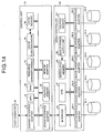
Fig. 14 is a block diagram showing a disk array device
according to Embodiment 2 of the present invention. The disk
array device shown in Fig. 14 is different from that shown in
Fig. 1 in the points that there is not provided in the control
unit 10 the nonvolatile memory 34 operable depending on a backup
power supply 36 even when power is down, that there are provided
in the array controller 50 the nonvolatile memory 34 and backup
power supply 36 in place thereof, and that there are provided
a volatile memory 23 and a logic circuit 37 for computing
exclusive-OR (EOR) in the array controller 50. As other
portions of the configuration are the same as those in
Embodiment 1 above, so that the same reference numerals are
assigned to the same components as those in the disk array device
shown in Fig. 1 and description thereof is omitted herein.
-
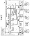
Fig. 15 and Fig. 16 are functional block diagrams each
showing the disk array device according to Embodiment 2 shown
in Fig. 14, and Fig. 15 shows a case where there is one faulty
disk device, while Fig. 16 shows a case where there is not faulty
disk device, namely a case where all the disk devices are
operating normally. Like in Embodiment 1 described above, in
Fig. 15 and Fig. 16, of a plurality units of disk device (5 units
in the figures) 32-1 to 32-5, for instance, the disk device 32-5
is used for storage of parity.
-
In the state where one disk device 32-2 is faulty, when
data (D0) in the specified disk device 32-1 is to be updated
to new data (D0 new), as shown in Fig. 15, new data (D0 new)
40, management table 41 for storing therein the status 42 and
the self-system flag 43, write flag 44, old data (Do old) 40-1,
other data (D2,D3) 46,47, old parity (Dp old) 48, and new parity
(Dp new) 48-1 are stored, like in Embodiment 1, in the
nonvolatile memory 34 of the array controller 50.
-
The new parity (Dp new) 48-1 is obtained by computing
exclusive-OR (EOR) among the old data (D0 old) 40-1, new data
(D0 new) 40, and old parity (Dp old) 48 in the logic circuit
37 provided in the array controller 50.
-
Also in this Embodiment 2, like in Embodiment 1, when the
processing for data write is to be executed, new data (D0 new)
40-2, other data (D2, D3) 46-1, 47-1 and new parity (Dp new)
48-2 are concurrently written in the disk devices 32-1, 32-3,
32-4, 32-5 according to the RAID3 system.
-
When write processing not finished in the normal state
is to be recovered, new data (D0 new) 40, other data (D2, D3)
46, 47, and new parity (Dp new) 48-1 stored in the nonvolatile
memory 34 are concurrently written via the device interface
adapters 54-1, 54-3, 54-4, 54-5 in the disk devices 32-1, 32-3,
32-4, 32-5 according to the RAID3 system.
-
When data (D0) in the specified disk device 32-1 is
updated to new data (D0 new) in the state where all the disk
devices 32-1, 32-2, 32-3, 32-4, 32-5 are operating normally,
as shown in Fig. 16, the new data (D0 new) 40, management table
41, and write flag 44 are stored in the nonvolatile memory 34
of the array controller 50. Also the old data (D0 old) 40-1
and old parity (Dp old) 48 are stored in the volatile memory
23 of the array controller 50.
-
The new data (D0 new) 40 stored in the nonvolatile memory
34 is written via the device interface adapter 54-1 in the disk
device 32-1. Also computing for exclusive-OR (EOR) among the
new data (D0 new) 40 stored in the nonvolatile memory 34, old
data (D0 old) 40-1 stored in the volatile memory 23, and old
parity (Dp old) 48 is executed in the logic circuit 37 to obtain
new parity (Dp new) 48-1, and the new parity is stored in the
volatile memory 23. This new parity (Dp new) 48-1 is written
via the device interface adapter 54-5 in the disk device 32-5.
-
When write processing not having been finished in the
normal state is to be recovered, the new data (D0 new) 40 stored
in the nonvolatile memory 34 is written via the device interface
adapter 54-1 in the disk device 32-1. Also data (D1, D2, D3)
are read out from the disk devices 32-2, 32-3, 32-4, sent to
and stored in the volatile memory 23.
-
Then new parity (Dp new) 48-1 is generated from the data
(D1, D2, D3) 45, 46, 47 stored in the volatile memory 23 and
new data (D0 new) 40 stored in the nonvolatile memory 34, and
the new parity (Dp new) 48-1 is written via the device interface
adapter 54-5 in the disk device 32-5.
-
Operations of the disk array device shown in Fig. 15 and
Fig. 16 are the same as those shown in the flow charts shown
in Fig. 6 to Fig. 13. For this reason description thereof is
omitted herein.
-
In Embodiment 2 shown in Fig. 14 to Fig. 16, the
nonvolatile memory 34 is provided in the array controller 50,
and if there is any faulty disk device when data is to be written,
new data (D0 new) 40, status 42, write flag 44, old data (D0
old) 40-1, old parity (Dp old) 48, other data (D2, D3) 46, 47,
and new parity (Dp new) 48-1 are stored in the nonvolatile memory
34, so that, even if processing for writing data and parity is
not finished in the normal state due to power failure or for
some other reasons, when power supply is restarted, the data
can easily be recovered by writing the new data (D0 new) 40,
other data (D2, D3) 46, 47, and new parity (Dp new) 48-1 stored
in the nonvolatile memory 34 in a disk device.
-
With the Embodiment 2 above, the nonvolatile memory 34
is provided in the array controller 50, and when data is to be
written in, if there is no faulty disk device, new data (D0 new)
40, status 42, and write flag 44 are stored in the nonvolatile
memory 34, so that, even if the processing for writing data and
parity is not finished in the normal state due to power failure
or for some other reasons, when power supply is restarted, data
(D1, D2, D3) belonging to the same parity group is read out from
disk devices other than a disk device, in which data is to be
updated, and a disk device for storage of parity, new parity
(Dp new) 48-1 is generated from the data (D1, D2, D3) and new
data (D0 new) 40 stored in the nonvolatile memory 34, the new
parity (Dp new) 48-1 and new data (D0 new) 40 are written anew
in a disk device, thus the data being easily recovered.
-
With the Embodiment 2 above, as the write flag 44 is stored
in the nonvolatile memory 34, after write operation is not
finished in the normal state, when power supply is restarted,
whether any data not having been written normally is left or
not can visually be checked by referring to the write flag 44,
so that the processing for data recovery can rapidly be
executed.
-
Further with the Embodiment 2, the status 42 is stored
in the nonvolatile memory 34, after write processing is not
finished in the normal state, when power supply is restarted,
the processing for recovery can be continued from the section
where the write processing is interrupted by referring to the
status 42, so that the processing for data recovery can rapidly
be executed.
-
Fig. 17 is a block diagram showing the disk array device
according to Embodiment 3 of the present invention. In the disk
array device according to this embodiment, as shown in Fig. 17
connected to the control unit 10 with the host computer 18
connected thereto are two units of array controller A50 and
array controller B51 driven by independent powers 62, 64
respectively, and for instance 5 units of disk device 32-1, 32-2,
32-3, 32-4, 32-5 are controlled by the array controller A50 and
array controller B51. It should be noted that the same
reference numerals are assigned to the same components as those
in the disk array device shown in Fig. 1 and detailed description
thereof is omitted herein.
-
Provided in the control unit 10 are, like in Embodiment
1, the MPU 12, ROM 20, volatile memory 22, cache function engine
24, cache memory 26, nonvolatile memory 34, back-up power supply
unit 36, resource manager module 13, service adapter 14, and
channel interface adapter 16.
-
Also to independently control the two units of array
controller A50 and array controller B51, provided in the control
unit 10 are a group A consisting of a device interface adapter
A17 and a device adapter module A11, and a group B consisting
of a device interface adapter B15 and a device adapter module
B19. These groups A and B are driven by the independent power
supply units 27, 28 respectively.
-
The array controller A50 has the same configuration as
that of the array controller B51, and although not shown in the
figure, there are provided, like in Embodiment 1 shown in Fig.
1, a plurality of device interface adapters functioning as an
upper interface connected to the device interface adapter A17
or device interface adapter B15 in the control unit 10 and a
lower interface with a plurality units of disk devices 32-1 to
32-5 connected thereto.
-
Fig. 18 is a functional block diagram showing the disk
array device according to Embodiment 3 shown in Fig. 17. In
Fig. 18, it is assumed that, of the plurality units of disk
devices 32-1 to 32-5 (for instance 5 units in the figure), the
disk device 32-5 is used for storage of parity. It is needless
to say that, in a case of the RAID4 system, the disk device 32-5
is always used for storage of parity, and that, in the RAID5
system, the disk device is used for storage of parity in data
access at the current point of time.
-
The nonvolatile memory 34 in the control unit 10 is shared
by the group A consisting of the device interface adapter A17
and device adapter module A11 and the group B consisting of the
device interface adapter B15 and device interface module B19.
Namely the data or parity stored in this nonvolatile memory 34
can be written via any of the two array controllers 50, 51 into
the disk devices 32-1, 32-2, 32-3, 32-4, and 32-5.
-
In the state where all the disk devices 32-1, 32-2, 32-3,
32-4, and 32-5 are operating normally, when data (D0) in the
instructed disk device 32-1 is to be updated to new data (D0
new), as shown in Fig. 18, stored in the nonvolatile memory 34
of the control unit 10 new data (D0 new) 40 transferred from
the host computer 18, old data (D0 old) 40-1 read out from the
disk device 32-1, old parity (Dp old) 48 read out from the disk
device for parity 32-5, management table 41 showing progression
of the write processing, and write flag 44 indicating that write
processing is being executed. Although there is no particular
limitation, the write flag 44 is stored in the management table
41.
-
Also the control unit 10 has a task generating section
72 for generating a task for writing back the new data (D0 new)
stored in the nonvolatile memory 34 into a disk device. The
task generating section 72 is realized by, for instance, the
MPU 12 in the control unit 10. The task information generated
in the task generating section 72 is stored in a task information
table 74 stored in a memory in the resource manager module 13,
and execution of the task processing is instructed to an
appropriate device adapter modules 11, 19 by the resource
manager according to the task information.
-
Also stored in the task information table 74 is an
alternative path processing request flag 76 indicating, when
an abnormal state is generated in one of the array controllers,
that write processing is executed by using an array controller
working normally in place of the array controller in which the
abnormal state has been generated.
-
The device adapter modules 11, 19 read out, when
instructed by the resource manager, task information from the
task information table 74, reads out new data (D0 new) 40 stored
in the nonvolatile memory 34 according to the task information,
and issues a write instruction to the array controllers 50, 51
in the system. Also the device adapter effects the write flag
44 in the management table 41 stored in the nonvolatile memory
34.
-
Each of the array controllers 50, 51 monitors, with a
power supply monitoring section 55, power supply state to the
another array controller 51 or 50, and when one of the array
controllers 50 (or 51) detects that power supply to another
array controller 51 (or 50) has been stopped, it is reported
by a power supply stop reporting section 56 via the device
interface adapter 17 (or 15) in the system to the device adapter
module 11 (or 19) that power supply to another array controller
51 (or 50) has been stopped. The power monitoring section 55
and power supply stop reporting section 56 are realized by a
microprocessor (MPU) or the like provided in the array
controllers 50, 51.
-
Also provided in the array controllers 50, 51 is a parity
generating section 57 for reading out other data in the same
parity group, to which the new data (D0 new) 40 transferred from
the nonvolatile memory 34 in the control unit 10 belongs, and
generating new parity (Dp new) from the data and new data (D0
new) 40.
-
Reconstruction of parity by this parity generating
section 57 is executed when a special mode is set with a flag
in response to a write instruction. The parity generating
section 57 is realized with a microprocessor (MPU) provided in
the array controllers 50, 51 or the like.
-
Next description is made for a flow of processing
operations by the disk array device shown in Fig. 18. The entire
operation flow in this disk array device, a flow of operations
for reading data, and a flow of recovery processing are almost
the same as those shown in flow charts shown in Fig. 6, Fig.
13, and Fig. 12, respectively. For this reason, description
of the entire operation flow, a flow of the recovery processing,
and that of the processing for reading data in the disk array
device shown in Fig. 18 is omitted herein.
-
Fig. 19 is a flow chart showing details of the write
processing in the disk array device shown in Fig. 18. In Fig.
19, when a write instruction is received from the host computer
18, at first a device adapter module A11 belonging to group A
in the control unit 10 issues a data write command to the array
controller A50 in the system in step S1671.
-
With this operation, in step S1672, the array controller
A50 writes new data (D0 new) according to the ordinary write
processing sequence shown in Fig. 9 in the disk device 32-1,
and also generates new parity (Dp new) from the new data (D0
new) 40, old data (D0 old), and old parity (Dp old), and writes
the new parity in the disk device for parity 32-5.
-
During the ordinary write processing in step S1672,
namely before the control unit 10 receives a write complete
signal from the array controller A50, if the control unit 10
receives an abnormal end signal in step S1673 and it is
determined in step S1674 that a cause for abnormal termination
is stop of power supply to the array controller A50, system
control shifts to step S1675.
-
In step S1675, the device adapter module A11 in which an
abnormal state has been detected sets an alternative path
processing request flag 76 in the task information table 74 to
have the write processing task, in which the abnormal state has
been generated, executed by another device path, namely by the
array controller B51. Then in step S1676, the device adapter
module A11 issues a request for the alternative path processing
for the task to the resource managers.
-
The resource manager, to which the alternative path
processing is requested, issues a request for execution of the
write processing task interrupted due to generation of an
abnormal state to the device adapter controlling the
alternative array controller B51 in step S1677.
-
The adapter having received the request recognizes, in
step S1678, that contents of the accepted processing is write
processing and at the same time, the alternative device path
processing to be executed in place of the array controller A50
with any abnormality having been generated therein, and in step
S1679, the adapter issues write instruction with a special flag
called herein as a parity generation flag for reconstruction
of parity data added thereto to the array controller B51.
-
The array controller B51 having received the write
instruction with the parity generation flag added thereto reads
out new data (D0 new) stored in the nonvolatile memory 34 in
the control unit 10, and writes the data in the disk device 32-1.
-
Then in step S1681, the array controller B51 reads out
data (D1, D2, D3) belonging to the same group to which the
update data belongs from other disk devices 32-2, 32-3, 32-4
excluding the disk device 32-1 in which data is to be updated
and the disk device for parity 32-5, generates new parity (Dp
new) by computing exclusive-OR (EOR) among the data (D1, D2,
D3) and new data (D0 new), and writes the new parity (Dp new)
in the disk device for parity 32-5.
-
Finally in step S1682, the alternative path processing
request flag 76 is invalidated, thus the data write processing
being finished.
-
In step S1674, if it is determined that a cause for
abnormal termination of the write processing is not due to stop
of power supply to the array controller A50, system control
shifts to step S1683. In step S1683, if it is determined that
a cause for abnormal termination of the write processing is due
to an abnormal operation, such as hung-up, of the array
controller A50, system control shifts to step S1684 to reset
the device interface adapter A17 and array controller A50, and
then in S1685 the parity generation flag for reconstruction of
parity data is added to the write instruction, which is again
issued to the array controller A50.
-
On the other hand, if it is determined that the cause for
abnormal termination of the write processing is interruption
of the write processing by the array controller A50 into a disk
device, system control directly shifts to step S1685 without
resetting the array controllers, a write instruction with the
parity generation flag for reconstruction of parity data added
thereto is again issued to the array controller A50.
-
The array controller A50 having received the write
instruction with the parity generation flag added thereto reads
out new data (D0 new) 40 stored in the nonvolatile memory 34
in the control unit 10 in step S1686, and writes the read-out
data in the disk device 32-1.
-
Then in step S1687, the array controller A50 reads out
data (D1, D2, D3) belonging to the same parity group to which
the data to be updated belongs from other disk devices 32-2,
32-3, 32-4 excluding the disk device 32-1 in which data updating
is executed and the disk device for parity 32-5, generates new
parity (Dp new) by computing exclusive-OR (EOR) among the
read-out data (D1, D2, D3) and new data (D0 new), and writes
the new parity in the disk device for parity 32-5. With this
operation, the data write operation is finished.
-
In step S1673 in Fig. 1, if an abnormal termination signal
is not received, it means that data updating by the array
controller A50 was executed normally, and the write processing
is finished immediately.
-
Fig. 20 is a flow chart showing detailed of the processing
for a write instruction to the other device issued to the array
controller A50 by a device adapter which has detected an
abnormal state in the array controller A50 in the disk array
device shown in Fig. 18. In Fig. 20, in step S1691 determination
is made as to whether there is a write instruction not having
received a normal termination complete signal from the array
controller A50 or not, and if it is determined that there is
a write instruction not having received the signal, in step
S1692 time-out is detected by the logic for monitoring the task
execution time by the resource manager.
-
Then in step S1693, the resource manager sets an
alternative path processing request flag 76 in the task
information table 74 to have a write processing task for the
write instruction not having received the normal termination
complete signal executed by another device path, namely by the
array controller B51.
-
Also the resource manager issues a request for processing
the write processing task for the write instruction not having
received the normal termination complete signal to the device
adapter module B19 controlling the alternative array controller
B51 in step S1694. The device adapter received the request
recognizes in step S1695 that contents of the received
processing is write processing and also alternative device path
processing in place of the array controller A50 in which an
abnormal state was generated, and issues in step S1696 a write
instruction with a special flag described herein as a parity
generation flag for reconstruction of parity data added thereto
to the array controller B51.
-
The array controller B51 having received the write
instruction with the parity generation flag added thereto reads
out new data (D0 new) 40 for the current write processing stored
in the nonvolatile memory 34 in the control unit 10, and writes
the read-out data in the disk device 32-1.
-
Then in step S1698, the array controller B51 reads out
data (D1, D2, D3) belonging to the same parity group to which
the data to be updated belongs from other disk devices 32-2,
32-3, 32-4 excluding the disk device 32-1 in which data is to
be updated and the disk device for parity 32-5, generates new
parity by computing exclusive-OR (EOR) among the read-out data
(D1, D2, D3) and new data (D0 new), and writes the new parity
in the disk device for parity 32-5.
-
Finally in step S1699, the alternative path processing
request flag 76 is invalidated, and the data write processing
is finished.
-
In step S1691, it is determined that there is any write
instruction not having received the normal termination complete
signal from the array controller A50, the processing is
terminated immediately.
-
With the Embodiment 3 shown in Fig. 17 to Fig. 20, the
nonvolatile memory 34 is provided in the control unit 10, and
when data is written in, the new data (D0 new) 40, a status
indicating a stage of write processing, and a management table
41 storing therein a flag indicating an array controller having
executed the processing shown in the status, old data (0 old)
40-1 and old parity (Dp old) 48 are stored in the nonvolatile
memory 34, so that, even if any abnormal state is generated in
one of the array controllers, the write processing can be
continued by another array controller in place of the array
controller in which the abnormal state was generated, and for
this reason data consistency can be maintained.
-
With the Embodiment 3 above, new data (D0 new) 40 and
management table 41 storing therein a status of write processing
and a flag indicating an array controller are stored in the
nonvolatile memory 34, so that, after the write processing for
writing data and parity is not finished in the normal state,
when power supply is restarted, data can easily be recovered
by reading out data (D1, D2, D3) belonging to the same parity
group from disk devices other than the disk device in which data
is to be updated and that for parity, generating new parity (Dp
new) 48-1 from the data (D1, D2, D3) and the new data (D0 new)
stored in the nonvolatile memory 34, and writing the new parity
(Dp new) 48-1 and new data (D0 new) anew in a disk device.
-
Fig. 21 is a functional block diagram showing a disk array
device according to Embodiment 4 of the present invention. In
this disk array device according to Embodiment 4, as shown in
Fig. 21, connected to the control unit 10 with the host computer
18 connected thereto are two units of array controller A50 and
array controller B51 driven by independent power supply units
62, 64 respectively, and for instance five units of disk devices
32-1, 32-2, 32-3, 32-4, and 32-5 are controlled by the array
controller A50 and array controller B51. It should be noted
that the same reference numerals are assigned to the same
components as those in the disk array device shown in Fig. 2
and detailed description thereof is omitted herein.
-
Although not shown in the figure, provided in the control
unit 10 are, like in Embodiment 1, an MPU, a ROM, a volatile
memory, a cache function engine, a cache memory, a resource
manager module, a service adapter, and a channel interface
adapter.
-
Configuration of the array controller A50 is the same as
that of the array controller B51, and although not shown herein,
like in Embodiment 1 shown in Fig. 2, a plurality units of
interface adapter functioning as an upper interface connected
to a device interface adapter not shown in the control unit 10,
and as a lower interface to which a plurality units of disk
devices 32-1 to 32-5 are connected are provided therein.
-
Also provided in the array controller A50 and array
controller B51 are nonvolatile memory 34 and back-up power
supply units (not shown) for supplying power to the nonvolatile
memory 34 respectively (not shown). The new data (D0 new) 40
transferred when data is to be written in a disk device, for
instance, from the control unit 10, old data (D0 old) 40-1 and
old parity (Dp old) 48 read out from the disk device, new parity
(Dp new) 48-1 newly generated, a status 42 indicating a stage
of write processing, and a management table 41 storing therein
a self-system flag indicating the array controller having
executed the processing shown in the status are stored in the
nonvolatile memory 34 in the array controller A50.
-
Stored in the nonvolatile memory 34 of the array
controller B51 are, for instance, at least new data (D0 new)
40-4, old data (D0 old) 40-5, and old parity (Dp old) 48-4.
-
Also a communicating section 82 for communication with
a controller in another device is provided in each of the array
controller A50 and array controller B51. Transaction of new
data (D0 new), old data (D0 old) and old parity (Dp old), and
a report of the normal termination of write processing is
executed through this communicating section 82. The
communicating sections 82 are connected to each other via a PCI
bus generally employed, for instance, in personal computers or
the like.
-
Also provided in each of the array controller A50 and
array controller B51 is a logic circuit 37 for preparing new
parity (Dp new) by computing exclusive-OR (EOR) among the new
data (D0 new), old data (D0 old), and old parity (Dp old).
-
Either one of the array controller A50 and array
controller B51 can write data or parity in the disk devices 32-1
to 32-5.
-
In the example shown in Fig. 21, it is assumed that, of
a plurality units of disk devices 32-1 to 32-5 (for instance,
5 units in the figure), for instance the disk device 32-5 is
used for storage of parity. It is needless to say that the disk
device 32-5 is always used for storage of parity in the RAID4
system, and that the disk device 32-5 is positioned as a disk
device for storage of parity in the current data access.
-
Fig. 22 shows a case where the management table 41, new
data (Do new), and new parity (Dp new) 48-1 are stored in the
nonvolatile memory 34 in the array controller A50. In this case,
although not shown in the figure, new data (D0 new) and new parity
(Dp new) are stored in the nonvolatile memory 34 in the array
controller B51.
-
Fig. 23 shows a case where the management table 41, new
data (D0 new) 40, intermediate parity (Dp int) 48-5 generated
by computing exclusive-OR (EOR) among old data (D0 old) and old
parity (Dp old) are stored in the nonvolatile memory 34 of the
array controller A50. In this case, although not shown in the
figure, new data (D0 new) and intermediate parity (Dp int) are
stored in the nonvolatile memory 34 in the array controller B51.
-
Next description is made for a flow of operational
sequence in the disk array device shown in Fig. 21. This entire
operational flow in this disk array and a flow of operations
for reading out data are substantially the same as those in
Fig. 6 and Fig. 13. So description of the entire operational
flow and an operational flow in data read processing in the disk
array device shown in Fig. 21 are omitted herein.
-
Fig. 24 is a flow chart showing details of the write
processing in the disk array device shown in Fig. 21. It should
be noted that a status of each step (a stage of write processing)
is also shown in the right side of the figure. In Fig. 24, at
first in step S2671, the array controller A50 receives new data
(D0 new) together with a write instruction from the control unit
10 and stores the new data (D0 new) 40 in the nonvolatile memory
34 in the array controller A50. The status in this step is
"Receive new data".
-
Then in step S2672, the array controller A50 transfers
new data (D0 new) via the communicating section 82 to the other
array controller B51, while the array controller B51 receives
the new data (D0 new) transferred thereto and stores the new
data (Do new) in the nonvolatile memory 34 in the array
controller B51. With this operation, the new data (D0 new) 40-4
is copied into the array controller B51. The status at this
point of time is " Receive new data".
-
Then in step S2673, the array controller A50 reads out
the old data (D0 old) and old parity from the disk devices 32-1,
32-5, and stores the old data (D0 old) 40-1 and old parity (Dp
old) 48 in the nonvolatile memory 34 in the array controller
A50. The status at this point of time is "Read old data &
parity".
-
Then in step S2674, the array controller A50 transfers
old data (D0 old) and old parity (Dp old) via the communicating
section 82 to the array controller B51, and on the other hand,
the array controller B51 receives and stores the old data (D0
old) and old parity (Dp old) transferred thereto in the
nonvolatile memory 34 in the array controller B51.
-
With this operation, the old data (D0 old) 40-5 and old
parity (Dp old) 48-4 have been copied. The status at this point
of time is " Read old data & parity".
-
Then in step S2675, the array controller A50 generates
new parity (Dp new) 48-1 from the new data (D0 new) 40, old data
(D0 old) 40-1, and old parity (Dp old) 48 stored in the
nonvolatile memory 34 in the array controller A50, and stores
the new parity in the nonvolatile memory 34 in the array
controller A50. The status at this point of time is "Generate
new parity".
-
Then in step S2676, the array controller A50 writes new
data (D0 new) 40 and new parity (Dp new) 48-1 at appropriate
places in the disk devices 32-1, 32-5. The status at this point
of time is "Write new data & parity".
-
Then in step S2677, the array controller A50 reports to
the control unit 10 that the write processing was finished in
the normal state. The status at this point of time is changed
from "Write new data & parity" to "Finish" after the report of
normal termination is complete.
-
Then in step S2678, the array controller A50 reports that
the write processing was finished in the normal state to the
array controller B51. The status at this point of time is
"Finish".
-
Then in step S2679, the array controller A50 releases the
region occupied by the new data (D0 new) 40, old data (D0 old)
40-1, old parity (Dp old), new parity (Dp new) 48-1 and status
42 stored in the nonvolatile memory 34 in the array controller
A50. The status at this point of time is "Finish".
-
In step S2680, the array controller B51 releases, when
having received the report of normal termination from the array
controller A50, the region occupied by the new data (D0 new)
40-4, old data (D0 old) 40-5, and old parity (Dp old) 48-4 stored
in the nonvolatile memory 34 in the array controller B51. The
status at this point of time is "Finish". With this operation,
the write processing is finished.
-
It should be noted that, when write processing is
interrupted due to generation of abnormal state such as stop
of power supply to the array controller A50, abnormal operations
of the array controller A50 such as hanging-up, or interruption
of write processing into a disk device by the array controller
A50, like in the write processing in Embodiment 3 shown in Fig.
19, the write processing may be continued by the array
controller B51 in place of the array controller A50.
-
Fig. 25 is a flow chart showing details of the recovery
processing in the disk array device shown in Fig. 21. In Fig.
25, when power is turned ON, at first in step S2861, the array
controller A50 (or B51) determines whether a controller in
another system, namely the array controller B51 (or A50) is
operating normally or not.
-
When the array controller B51 (or A50) is operating
normally, in step S2862, whether the write processing in the
system, namely by the array controller A50 (or B51) has been
finished by the array controller B51 (or A50) or not.
-
When the write processing in the system has not been
finished, in step S2683, arbitrary is made as to which of the
array control A50 and array controller B51 should execute the
write processing not finished yet. This arbitration may be
executed, for instance, in the way where either one of the array
controller A50 and array controller B51 started first becomes
a master and the one started later becomes a slave one (contrary
one is also allowable), and the controller positioned as a
master executes the write processing. At previously priority
orders of primary and secondary ones are assigned to the array
controller A50 and array controller B51, and the primary
controller may execute the write processing.
-
When a controller, which executes the write processing,
is fixed through arbitration, the array controller taking
charge for the write processing reads out in step S2864 new data
(D0 new) from the nonvolatile memory 34 in the array controller,
and also reads out the status 42 from the nonvolatile memory
34 in the array controller A50, and in step S2865 restarts the
write processing from the interrupted section according to the
read-out status.
-
When the write processing is finished, in step 2866, the
array controller having restarted the write processing reports
to the control unit 10 that the write processing was finished
in the normal state, and also reports in step S2867 to the other
array controller that the write processing was finished in the
normal state.
-
Then in step S2868, the array controller having restarted
the write processing releases a region for new data (D0 new),
old data (D0 old), old parity (Dp old) each stored in the
nonvolatile memory 34 in the array controller, or a region for
new parity (Dp new) when new parity is stored therein, or a region
for status when a status is stored therein.
-
Also in step S2869, also the array controller not having
taken charge for restart of the write processing releases a
region for new data (D0 new), old data (D0 old), old parity (Dp
old) each stored in the nonvolatile memory 34 in the array
controller, or a region for new parity (Dp new) when new parity
is stored therein, or a region for status when status is stored
therein. With this operation, the recovery processing is
finished.
-
In step S2862, if the write processing in the system has
been finished, the write processing is not restarted, system
control shifts to step S2866 to report normal termination of
the write processing (step S2866 to S2867) and also releases
a region in the nonvolatile memory 34 (step S2868 to S2869),
and the recovery processing is finished.
-
Also in step S2861, if the array controller B51 (or A50)
in the other system is not operating normally, system control
shifts to step S2864, the array controller A50 (or B51) in the
current system restarts the write processing to execute the
operations in step S2864 to S2869, and the recovery processing
is finished.
-
It should be noted that the same operational sequence
is followed when the management table 41, new data (D0 new) 40,
and new parity (Dp new) 48-1 are stored in the nonvolatile memory
34 as shown in Fig. 22, or when the management table 41, new
data (D0 new) 40, intermediate parity (Dp int) 48-5 are stored
in the nonvolatile memory 34 as shown in Fig. 23.
-
With Embodiment 4 shown in Fig. 21 to Fig. 25, the
nonvolatile memory 34 is provided in each of the array
controller A50 and array controller B51, and when data is
written in, new data (D0 new) 40, status 42 indicating a stage
of write processing, old data (D0 old) 40-1, old parity (Dp old)
48, new parity (Dp new) 48-1 or the like are stored in the
nonvolatile memory 34 of the array controller A50, and further
each of the data is copied in the nonvolatile memory 34 of the
array controller B51, so that, even if the processing for
writing data or parity is not finished in the normal state due
to power failure or for some other reason, when power supply
is restarted, the data can easily be recovered by using the new
data stored in the nonvolatile memory 34 in the array controller
A50 or in the nonvolatile memory 34 of the array controller B51.
-
Further with Embodiment 4 above, if any abnormality is
generated in the write processing by one of the array
controllers, the write processing can be continued by another
controller in place of the array controller in which abnormality
was generated, so that data consistency can be maintained.
-
Fig. 26 is a functional block diagram showing a disk array
device according to Embodiment 5 of the present invention. In
this disk array device according to Embodiment 5, as shown in
Fig. 26, connected to the control unit 10 with the host computer
18 connected thereto are two units of array controller A50 and
array controller B51 driven by independent power supply units
62, 64, respectively, and for instance 5 units of disk devices
32-1, 32-2, 32-3, 32-4, and 32-5 are controlled by the array
controller A50 and array controller B51, and a shared device
90 having the nonvolatile memory 34, which can be used to write
data in or read data from by either one of the array controller
A50 and array controller B51, is connected to the array
controller A50 as well as to the array controller B51.
-
Power is applied to this nonvolatile memory 34 from a
back-up power supply unit 91. It should be noted that the same
reference numerals are assigned to the same components as those
in the disk array device shown in Fig. 2 and description thereof
is omitted herein.
-
Although not shown in the figure, provided in the control
unit 10 are, like in Embodiment 1, an MPU, a ROM, a volatile
memory, a cache function engine, a cache memory, a resource
manager module, a service adapter, and a channel interface
adapter.
-
Configuration of the array controller A50 is the same as
that of the array controller B51, and although now shown herein,
like in Embodiment 1 shown in Fig. 2, a plurality units of device
interface adapter functioning as an upper interface connected
to a device interface adapter not shown in the control unit 10,
and as a lower interface to which a plurality units of disk
devices 32-1 to 32-5 are connected are provided therein.
-
Also provided in each of the array controller A50 and
array controller B51 is a logic circuit for preparing new parity
(Dp new) by computing exclusive-OR (EOR) among the new data (D0
new), old data (D0 old), and old parity (Dp old).
-
Both the array controller A50 and array controller B51
can write data or parity in the disk devices 32-1 to 32-5.
-
When data is written in a disk device, new data (D0 new)
40-6, old data (D0 old) 40-7, old parity (Dp old) 48-6, and
management table 41-1 with management information such as
status 42 stored therein transferred from the array controller
executing the write processing (array controller A50 in the
figure) is stored in the nonvolatile memory 34.
-
Also in this disk array device, provided in each of the
array controller A50 and array controller B51 is a power
monitoring section 93 for mutually monitoring power supply
state in the other array controller, so that power supply state
in an array controller during write processing can always be
monitored. The power monitoring section 93 for instance
periodically sends a message to the other array controller, and
monitors a response to the message.
-
In the example shown in Fig. 26, it is assumed that, of
a plurality of disk devices 32-1 to 32-5 (for instance 5 units
in the figure), the disk device 32-5 is used for storage of parity.
It is needless to say that, in a case of the RAID4, the disk
device 32-5 is always used for storage of parity, and that, in
a case of the RAID5, the disk device 32-5 is positioned as that
for storage of parity in the current data access.
-
Fig. 27 shows an example of contents of the management
table stored in the nonvolatile memory 34 in the shared device
90. As shown in the figure, stored in the management table 41-1
are "op_id" indicating for instance an identifier for
differentiating each write processing; "data LBA" indicating
a logical block address as an object for the current write
processing; "old data address" indicating an address where old
data (D0 old) is temporally stored; "new data address"
indicating an address where new data (D0 new) is temporally
stored; "old parity address" indicating an address where old
parity (Dp old) is temporally stored; "new parity address"
indicating an address where new parity (Dp new) is temporally
stored; "array controller #" indicating an identifier such as
a number identifying an array controller which manages this
management table 41-1; and "write status" indicating a current
status of write processing.
-
Next description is made for an operational flow in the
disk array device shown in Fig. 26. The entire operational flow,
a flow of operations for reading out data, and an operational
for recovery processing in this disk array device are
substantially the same as those shown in the flow charts in Fig.
6, Fig. 13, and Fig. 12, respectively. For this reason, the
entire operations, a flow of operations in the recovery
processing, and that of the data read processing in the disk
array device shown in Fig. 26 are omitted herein.
-
Fig. 28 is a flow chart showing details of the write
processing in the disk array device in Fig. 26. In Fig. 28,
when the control unit 10 receives a write command from the host
computer 18, at first in step S3671, the control unit 10 issues
a data write instruction to the array controller A50.
-
When the array controller A50 receives new data (D0 new)
40 together with the write instruction, in step S3672 the array
controller A50 stores the new data (D0 new) 40-6, old data (D0
old) 40-7, old parity (Dp old) 48-6, and management table 41-1
in the nonvolatile memory 34 in the shared device 90, then in
step S3673 writes the new data (D0 new) 40 in the disk device
32-1 and also generates new parity (Dp new) from the new data
(D0 new) 40, old data (D0 old) 40-1, and old parity (Dp old)
48, and starts the normal write processing to write the new
parity in the disk device 32-5 for storage of parity.
-
During the normal write processing, if power supply to
the array controller currently executing the write processing,
namely power supply to the array controller A50 is disconnected,
in step S3674 the power monitoring section 93 detects
disconnection of the power, and in step S3675 reports
disconnection of the power to the array controller A50 to the
other array controller, namely to the array controller B51.
-
In step S3676, the array controller B51 having received
the report of disconnection of power reads out new data (D0 new)
40-6, old data (D0 old) 40-7, old parity (Dp old) 48-6 , and
management information in the management table 41-4 from the
nonvolatile memory 34 in the shared device 90, and in step S3677
the array controller B51 continues the interrupted write
processing in place of the array controller A50.
-
Then in step S3678, after the write processing by the
array controller B51 is finished, a region of the nonvolatile
memory 34 in the shared device 90 is released, and the write
processing is finished.
-
In step S3674, when disconnection of power to the array
controller A50 is not detected, system control shifts to step
S3678, a region of the nonvolatile in the shared memory 90 is
released, and the write processing is finished.
-
Fig. 29 shows a case where, in place of the power
monitoring section 93 for monitoring disconnection of power to
the array controller as shown in Fig. 26, a controller
monitoring section 95 for monitoring operations of the array
controllers 50, 51 is provided in each of the array controllers
50, 51, and power supply to other controller is periodically
monitored by this controller monitoring section 95 at a
prespecified time interval. Other portions of the
configuration are the same as those in Fig. 26, and detailed
description thereof is omitted herein.
-
The controller monitoring section 95, for instance,
periodically sends a message to the other array controller, and
motors a response to the message.
-
Next description is made for a flow of operations in the
disk array device shown in Fig. 29. A general operation flow,
a flow of operations in the data read processing, and a flow
of operations in the recovery processing are the same as those
in the device shown in Fig. 26, namely are substantially the
same as those shown in the flow charts in Fig. 6, Fig. 13, and
Fig. 12 respectively. For this reason, description of the
general operation flow and flows of operations in the recovery
processing and in the data read processing is omitted herein.
-
Fig. 30 is a flow chart showing details of the write
processing in the disk array device shown in Fig. 29. In Fig.
30, when the control unit 10 receives a write command from the
host computer 18, at first in step S3681 the control unit 10
issues a data write instruction to the array controller A50.
-
When the array controller A50 receives new data (D0 new)
40 together with the write instruction, in step S3682 the array
controller A50 stores the new data (D0 new) 40-6, old data (D0
old) 40-7, old parity (Dp old) 48-6, and management table 41-1
in the nonvolatile memory 34 in the shared device 90, and then
in step S3683 writes the new data (D0 new) 40 in the disk device
32-1, and also generates new parity (Dp new) from the new data
(D0 new) 40, old data (D0 old) 40-1, old parity (Dp old) 48,
and starts the normal write operation to write the new parity
(Dp new) in the disk device 32-5 for parity.
-
During this ordinary write processing, if power supply
to the array controller executing the write operation, namely
power to the array controller A50 is disconnected, in step S3684
the controller monitoring section 95 in the array controller
B51 monitoring operating state of the array controller A50 at
a prespecified interval detects disconnection of the power.
Then in step S3685, the array controller B51 determines, by
referring to the status of write processing stored in the
nonvolatile memory 34 in the shared device 90, whether the array
controller A50 was executing the write processing or not at the
point of time when power to the array controller A50 was cut.
-
If it is determined that the array controller was
executing the write processing when the power supply was
disconnected, in step S3686 the array controller B51 reads out
the new data (D0 new) 40-6, old data (D0 old) 40-7, old parity
(Dp old) 48-6, and management information in the management
table 41-1 from the nonvolatile memory 34 in the shared device
90, and in step 3687 restarts the interrupted write processing
in place of the array controller A50.
-
Then in step S3688, after the write processing by the
array controller B51 is finished, a region of the nonvolatile
memory 34 in the shared device 90 is released, and the write
processing is finished.
-
In step S3684, if disconnection of power supply to the
array controller A50 is not detected, or if it is determined
in step S3685 that the array controller A50 was not executing
the write processing when power was cut, system control shifts
to step S3688, a region of the nonvolatile memory 34 in the shared
device 90 is released, and the write processing is finished.
-
With Embodiment 5 shown in Fig. 26 to Fig. 30, the
nonvolatile memory 34 is provided in the shared device 90
accessible from both the array controller A50 and array
controller B51, and when the data write processing is started,
the new data (D0 new) 40-6, old data (D0 old) 40-7, old parity
(Dp old) 48-6, and management table 41-1 including status or
the like therein are stored in the nonvolatile memory 34, so
that, when any abnormality is generated in the write processing
by one of the array controllers, the other array controller can
continue the write processing in place f the faulty array
controller, and for this reason consistency of data can be
maintained.
-
With Embodiment 5 above, even if write processing is not
finished in the normal state due to power failure to the entire
system or for some other reason during the processing for
writing data and parity, when power supply is restarted, the
data can easily be recovered by using the data and management
information stored in the nonvolatile memory 34 in the shared
device 90.
-
Fig. 31 is a functional block diagram showing the disk
array device according to Embodiment 6 of the present invention.
In this disk array device according to this embodiment, as shown
in Fig. 31, connected to the control unit 10 with the host
computer 18 connected thereto is an array controller 50, and
for instance 5 units of disk devices 32-1, 32-2, 32-3, 32-4,
32-5 are controlled by the array controller 50. Power is
supplied from a non-failure power supply unit 98 to the array
controller 50 as well as to all the disk devices 32-1 to 32-5.
It should be noted that the same reference numerals are assigned
to the same components as those in the disk array device shown
in Fig. 2, and detailed description is omitted herein.
-
Generally, inconsistency in data stored the disk devices
32-1 to 32-5 is generated when write processing is interrupted
due to stop of power supply to the disk devices 32-1 to 32-5
or to the array controller 50 during the write processing to
the disk devices.
-
The non-failure power supply unit 98 incorporates a
battery therein, and in a case where, for instance, supply of
AC power is stopped due to power failure or for some other reason,
power to the disk devices 32-1 to 32-5 or to the array controller
50 is backed up by the battery until the write processing being
executed by the array controller 50 at the point of time when
the AC power supply was stopped is finished.
-
With Embodiment 6 shown in Fig. 31, power for the array
controller 50 is backed up by the non-failure power supply unit
98, so that power supply can continuously be executed even when
AC input to the power supply unit is stopped or when power supply
from the power supply unit to the array controller 50 is stopped
due to any trouble, the write processing by the array controller
50 is not interrupted, and generation of inconsistency in data
can be prevented.
-
Also with Embodiment 6 above, power supply to the disk
devices 32-1 to 32-5 is backed up by the non-failure power supply
unit 98, so that power supply can be continued even when power
supply from a power supply unit to the disk devices 32-1 to 32-5
is stopped due to any trouble, the write processing by the array
controller 50 is not interrupted, and generation of
inconsistency in data can be prevented.
-
It should be noted that the present invention is not
limited to the embodiments described above, and it is needless
to say that various modifications and changes in the design are
possible within the gist of the invention.
-
Description of the embodiments above assumes a case of
recovery processing executed, after power supply is
disconnected during write processing, when power supply is
restarted, but the present invention can be applied, in addition
to a case where some trouble is generated due to disconnection
of power, to the recovery processing where write processing is
not finished in the normal state due to generation of some other
fatal troubles during write processing.
-
With the present invention, when write processing once
interrupted due to power failure or for some other reason is
restarted, processing for data recovery is executed by
generating new parity using data and parity stored at positions
corresponding to disk write positions for new data in a disk
device in which new data is to be written as well as in a disk
device for parity and also new data stored in a nonvolatile
memory, data can easily be executed even when there is any faulty
disk device. Namely in the conventional technology, if there
is any faulty disk device, when it is tried to execute processing
for data recovery because there is no consistency in parity at
the restarting of write processing once interrupted, in the
conventional technology, the parity cannot be reproduced
because data required for recovery cannot be normally read out
from the faulty disk device, namely processing for data recovery
cannot be executed, but with the present invention, it is
possible to overcome the inconvenience.
-
This application is based on Japanese patent application
No. HEI 9-302331 filed in the Japanese Patent Office on November
4, 1997, the entire contents of which are hereby incorporated
by reference.
-
Although the invention has been described with respect
to a specific embodiment for a complete and clear disclosure,
the appended claims are not to be thus limited but are to be
construed as embodying all modifications and alternative
constructions that may occur to one skilled in the art which
fairly fall within the basic teaching herein set forth.