EP0915516A2 - Substrate for stacked module and stacked module - Google Patents
Substrate for stacked module and stacked module Download PDFInfo
- Publication number
- EP0915516A2 EP0915516A2 EP98120397A EP98120397A EP0915516A2 EP 0915516 A2 EP0915516 A2 EP 0915516A2 EP 98120397 A EP98120397 A EP 98120397A EP 98120397 A EP98120397 A EP 98120397A EP 0915516 A2 EP0915516 A2 EP 0915516A2
- Authority
- EP
- European Patent Office
- Prior art keywords
- chip select
- electrodes
- electrode
- substrates
- substrate
- Prior art date
- Legal status (The legal status is an assumption and is not a legal conclusion. Google has not performed a legal analysis and makes no representation as to the accuracy of the status listed.)
- Withdrawn
Links
- 239000000758 substrate Substances 0.000 title claims abstract description 142
- 239000004065 semiconductor Substances 0.000 claims abstract description 77
- 239000004020 conductor Substances 0.000 claims description 15
- 238000004806 packaging method and process Methods 0.000 description 8
- 230000006870 function Effects 0.000 description 4
- 229910000679 solder Inorganic materials 0.000 description 4
- 239000000919 ceramic Substances 0.000 description 3
- 239000011521 glass Substances 0.000 description 2
- 239000012212 insulator Substances 0.000 description 2
- 238000000034 method Methods 0.000 description 2
- 238000010586 diagram Methods 0.000 description 1
- 238000004519 manufacturing process Methods 0.000 description 1
- 239000011159 matrix material Substances 0.000 description 1
- 239000011347 resin Substances 0.000 description 1
- 229920005989 resin Polymers 0.000 description 1
Images


Classifications
-
- H—ELECTRICITY
- H05—ELECTRIC TECHNIQUES NOT OTHERWISE PROVIDED FOR
- H05K—PRINTED CIRCUITS; CASINGS OR CONSTRUCTIONAL DETAILS OF ELECTRIC APPARATUS; MANUFACTURE OF ASSEMBLAGES OF ELECTRICAL COMPONENTS
- H05K1/00—Printed circuits
- H05K1/02—Details
- H05K1/14—Structural association of two or more printed circuits
- H05K1/144—Stacked arrangements of planar printed circuit boards
-
- H—ELECTRICITY
- H01—ELECTRIC ELEMENTS
- H01L—SEMICONDUCTOR DEVICES NOT COVERED BY CLASS H10
- H01L23/00—Details of semiconductor or other solid state devices
- H01L23/48—Arrangements for conducting electric current to or from the solid state body in operation, e.g. leads, terminal arrangements ; Selection of materials therefor
- H01L23/488—Arrangements for conducting electric current to or from the solid state body in operation, e.g. leads, terminal arrangements ; Selection of materials therefor consisting of soldered or bonded constructions
- H01L23/498—Leads, i.e. metallisations or lead-frames on insulating substrates, e.g. chip carriers
- H01L23/49811—Additional leads joined to the metallisation on the insulating substrate, e.g. pins, bumps, wires, flat leads
- H01L23/49816—Spherical bumps on the substrate for external connection, e.g. ball grid arrays [BGA]
-
- H—ELECTRICITY
- H01—ELECTRIC ELEMENTS
- H01L—SEMICONDUCTOR DEVICES NOT COVERED BY CLASS H10
- H01L23/00—Details of semiconductor or other solid state devices
- H01L23/48—Arrangements for conducting electric current to or from the solid state body in operation, e.g. leads, terminal arrangements ; Selection of materials therefor
- H01L23/488—Arrangements for conducting electric current to or from the solid state body in operation, e.g. leads, terminal arrangements ; Selection of materials therefor consisting of soldered or bonded constructions
- H01L23/498—Leads, i.e. metallisations or lead-frames on insulating substrates, e.g. chip carriers
- H01L23/49833—Leads, i.e. metallisations or lead-frames on insulating substrates, e.g. chip carriers the chip support structure consisting of a plurality of insulating substrates
-
- H—ELECTRICITY
- H01—ELECTRIC ELEMENTS
- H01L—SEMICONDUCTOR DEVICES NOT COVERED BY CLASS H10
- H01L25/00—Assemblies consisting of a plurality of individual semiconductor or other solid state devices ; Multistep manufacturing processes thereof
- H01L25/03—Assemblies consisting of a plurality of individual semiconductor or other solid state devices ; Multistep manufacturing processes thereof all the devices being of a type provided for in the same subgroup of groups H01L27/00 - H01L33/00, or in a single subclass of H10K, H10N, e.g. assemblies of rectifier diodes
- H01L25/04—Assemblies consisting of a plurality of individual semiconductor or other solid state devices ; Multistep manufacturing processes thereof all the devices being of a type provided for in the same subgroup of groups H01L27/00 - H01L33/00, or in a single subclass of H10K, H10N, e.g. assemblies of rectifier diodes the devices not having separate containers
- H01L25/065—Assemblies consisting of a plurality of individual semiconductor or other solid state devices ; Multistep manufacturing processes thereof all the devices being of a type provided for in the same subgroup of groups H01L27/00 - H01L33/00, or in a single subclass of H10K, H10N, e.g. assemblies of rectifier diodes the devices not having separate containers the devices being of a type provided for in group H01L27/00
- H01L25/0657—Stacked arrangements of devices
-
- H—ELECTRICITY
- H01—ELECTRIC ELEMENTS
- H01L—SEMICONDUCTOR DEVICES NOT COVERED BY CLASS H10
- H01L2224/00—Indexing scheme for arrangements for connecting or disconnecting semiconductor or solid-state bodies and methods related thereto as covered by H01L24/00
- H01L2224/01—Means for bonding being attached to, or being formed on, the surface to be connected, e.g. chip-to-package, die-attach, "first-level" interconnects; Manufacturing methods related thereto
- H01L2224/02—Bonding areas; Manufacturing methods related thereto
- H01L2224/04—Structure, shape, material or disposition of the bonding areas prior to the connecting process
- H01L2224/0401—Bonding areas specifically adapted for bump connectors, e.g. under bump metallisation [UBM]
-
- H—ELECTRICITY
- H01—ELECTRIC ELEMENTS
- H01L—SEMICONDUCTOR DEVICES NOT COVERED BY CLASS H10
- H01L2224/00—Indexing scheme for arrangements for connecting or disconnecting semiconductor or solid-state bodies and methods related thereto as covered by H01L24/00
- H01L2224/01—Means for bonding being attached to, or being formed on, the surface to be connected, e.g. chip-to-package, die-attach, "first-level" interconnects; Manufacturing methods related thereto
- H01L2224/02—Bonding areas; Manufacturing methods related thereto
- H01L2224/04—Structure, shape, material or disposition of the bonding areas prior to the connecting process
- H01L2224/05—Structure, shape, material or disposition of the bonding areas prior to the connecting process of an individual bonding area
- H01L2224/0554—External layer
- H01L2224/05541—Structure
- H01L2224/05548—Bonding area integrally formed with a redistribution layer on the semiconductor or solid-state body
-
- H—ELECTRICITY
- H01—ELECTRIC ELEMENTS
- H01L—SEMICONDUCTOR DEVICES NOT COVERED BY CLASS H10
- H01L2224/00—Indexing scheme for arrangements for connecting or disconnecting semiconductor or solid-state bodies and methods related thereto as covered by H01L24/00
- H01L2224/01—Means for bonding being attached to, or being formed on, the surface to be connected, e.g. chip-to-package, die-attach, "first-level" interconnects; Manufacturing methods related thereto
- H01L2224/02—Bonding areas; Manufacturing methods related thereto
- H01L2224/04—Structure, shape, material or disposition of the bonding areas prior to the connecting process
- H01L2224/05—Structure, shape, material or disposition of the bonding areas prior to the connecting process of an individual bonding area
- H01L2224/0554—External layer
- H01L2224/0556—Disposition
- H01L2224/0557—Disposition the external layer being disposed on a via connection of the semiconductor or solid-state body
-
- H—ELECTRICITY
- H01—ELECTRIC ELEMENTS
- H01L—SEMICONDUCTOR DEVICES NOT COVERED BY CLASS H10
- H01L2224/00—Indexing scheme for arrangements for connecting or disconnecting semiconductor or solid-state bodies and methods related thereto as covered by H01L24/00
- H01L2224/01—Means for bonding being attached to, or being formed on, the surface to be connected, e.g. chip-to-package, die-attach, "first-level" interconnects; Manufacturing methods related thereto
- H01L2224/10—Bump connectors; Manufacturing methods related thereto
- H01L2224/12—Structure, shape, material or disposition of the bump connectors prior to the connecting process
- H01L2224/13—Structure, shape, material or disposition of the bump connectors prior to the connecting process of an individual bump connector
- H01L2224/13001—Core members of the bump connector
- H01L2224/1302—Disposition
- H01L2224/13024—Disposition the bump connector being disposed on a redistribution layer on the semiconductor or solid-state body
-
- H—ELECTRICITY
- H01—ELECTRIC ELEMENTS
- H01L—SEMICONDUCTOR DEVICES NOT COVERED BY CLASS H10
- H01L2224/00—Indexing scheme for arrangements for connecting or disconnecting semiconductor or solid-state bodies and methods related thereto as covered by H01L24/00
- H01L2224/01—Means for bonding being attached to, or being formed on, the surface to be connected, e.g. chip-to-package, die-attach, "first-level" interconnects; Manufacturing methods related thereto
- H01L2224/10—Bump connectors; Manufacturing methods related thereto
- H01L2224/12—Structure, shape, material or disposition of the bump connectors prior to the connecting process
- H01L2224/13—Structure, shape, material or disposition of the bump connectors prior to the connecting process of an individual bump connector
- H01L2224/13001—Core members of the bump connector
- H01L2224/1302—Disposition
- H01L2224/13025—Disposition the bump connector being disposed on a via connection of the semiconductor or solid-state body
-
- H—ELECTRICITY
- H01—ELECTRIC ELEMENTS
- H01L—SEMICONDUCTOR DEVICES NOT COVERED BY CLASS H10
- H01L2224/00—Indexing scheme for arrangements for connecting or disconnecting semiconductor or solid-state bodies and methods related thereto as covered by H01L24/00
- H01L2224/01—Means for bonding being attached to, or being formed on, the surface to be connected, e.g. chip-to-package, die-attach, "first-level" interconnects; Manufacturing methods related thereto
- H01L2224/10—Bump connectors; Manufacturing methods related thereto
- H01L2224/15—Structure, shape, material or disposition of the bump connectors after the connecting process
- H01L2224/16—Structure, shape, material or disposition of the bump connectors after the connecting process of an individual bump connector
- H01L2224/161—Disposition
- H01L2224/16135—Disposition the bump connector connecting between different semiconductor or solid-state bodies, i.e. chip-to-chip
- H01L2224/16145—Disposition the bump connector connecting between different semiconductor or solid-state bodies, i.e. chip-to-chip the bodies being stacked
- H01L2224/16146—Disposition the bump connector connecting between different semiconductor or solid-state bodies, i.e. chip-to-chip the bodies being stacked the bump connector connecting to a via connection in the semiconductor or solid-state body
-
- H—ELECTRICITY
- H01—ELECTRIC ELEMENTS
- H01L—SEMICONDUCTOR DEVICES NOT COVERED BY CLASS H10
- H01L2225/00—Details relating to assemblies covered by the group H01L25/00 but not provided for in its subgroups
- H01L2225/03—All the devices being of a type provided for in the same subgroup of groups H01L27/00 - H01L33/648 and H10K99/00
- H01L2225/04—All the devices being of a type provided for in the same subgroup of groups H01L27/00 - H01L33/648 and H10K99/00 the devices not having separate containers
- H01L2225/065—All the devices being of a type provided for in the same subgroup of groups H01L27/00 - H01L33/648 and H10K99/00 the devices not having separate containers the devices being of a type provided for in group H01L27/00
- H01L2225/06503—Stacked arrangements of devices
- H01L2225/0652—Bump or bump-like direct electrical connections from substrate to substrate
-
- H—ELECTRICITY
- H01—ELECTRIC ELEMENTS
- H01L—SEMICONDUCTOR DEVICES NOT COVERED BY CLASS H10
- H01L2225/00—Details relating to assemblies covered by the group H01L25/00 but not provided for in its subgroups
- H01L2225/03—All the devices being of a type provided for in the same subgroup of groups H01L27/00 - H01L33/648 and H10K99/00
- H01L2225/04—All the devices being of a type provided for in the same subgroup of groups H01L27/00 - H01L33/648 and H10K99/00 the devices not having separate containers
- H01L2225/065—All the devices being of a type provided for in the same subgroup of groups H01L27/00 - H01L33/648 and H10K99/00 the devices not having separate containers the devices being of a type provided for in group H01L27/00
- H01L2225/06503—Stacked arrangements of devices
- H01L2225/06527—Special adaptation of electrical connections, e.g. rewiring, engineering changes, pressure contacts, layout
-
- H—ELECTRICITY
- H01—ELECTRIC ELEMENTS
- H01L—SEMICONDUCTOR DEVICES NOT COVERED BY CLASS H10
- H01L2225/00—Details relating to assemblies covered by the group H01L25/00 but not provided for in its subgroups
- H01L2225/03—All the devices being of a type provided for in the same subgroup of groups H01L27/00 - H01L33/648 and H10K99/00
- H01L2225/04—All the devices being of a type provided for in the same subgroup of groups H01L27/00 - H01L33/648 and H10K99/00 the devices not having separate containers
- H01L2225/065—All the devices being of a type provided for in the same subgroup of groups H01L27/00 - H01L33/648 and H10K99/00 the devices not having separate containers the devices being of a type provided for in group H01L27/00
- H01L2225/06503—Stacked arrangements of devices
- H01L2225/06541—Conductive via connections through the device, e.g. vertical interconnects, through silicon via [TSV]
-
- H—ELECTRICITY
- H01—ELECTRIC ELEMENTS
- H01L—SEMICONDUCTOR DEVICES NOT COVERED BY CLASS H10
- H01L2225/00—Details relating to assemblies covered by the group H01L25/00 but not provided for in its subgroups
- H01L2225/03—All the devices being of a type provided for in the same subgroup of groups H01L27/00 - H01L33/648 and H10K99/00
- H01L2225/04—All the devices being of a type provided for in the same subgroup of groups H01L27/00 - H01L33/648 and H10K99/00 the devices not having separate containers
- H01L2225/065—All the devices being of a type provided for in the same subgroup of groups H01L27/00 - H01L33/648 and H10K99/00 the devices not having separate containers the devices being of a type provided for in group H01L27/00
- H01L2225/06503—Stacked arrangements of devices
- H01L2225/06572—Auxiliary carrier between devices, the carrier having an electrical connection structure
-
- H—ELECTRICITY
- H01—ELECTRIC ELEMENTS
- H01L—SEMICONDUCTOR DEVICES NOT COVERED BY CLASS H10
- H01L2924/00—Indexing scheme for arrangements or methods for connecting or disconnecting semiconductor or solid-state bodies as covered by H01L24/00
- H01L2924/095—Indexing scheme for arrangements or methods for connecting or disconnecting semiconductor or solid-state bodies as covered by H01L24/00 with a principal constituent of the material being a combination of two or more materials provided in the groups H01L2924/013 - H01L2924/0715
- H01L2924/097—Glass-ceramics, e.g. devitrified glass
- H01L2924/09701—Low temperature co-fired ceramic [LTCC]
-
- H—ELECTRICITY
- H05—ELECTRIC TECHNIQUES NOT OTHERWISE PROVIDED FOR
- H05K—PRINTED CIRCUITS; CASINGS OR CONSTRUCTIONAL DETAILS OF ELECTRIC APPARATUS; MANUFACTURE OF ASSEMBLAGES OF ELECTRICAL COMPONENTS
- H05K1/00—Printed circuits
- H05K1/02—Details
- H05K1/11—Printed elements for providing electric connections to or between printed circuits
- H05K1/111—Pads for surface mounting, e.g. lay-out
- H05K1/112—Pads for surface mounting, e.g. lay-out directly combined with via connections
Definitions
- This invention relates to a packaging structure in which a semiconductor device such as a memory or the like is used, and particularly to a stacked module formed by stacking semiconductor devices and connecting them and substrates used for the stacked module, in which a semiconductor device is mounted on the surface thereof, to be stacked.
- a known packaging method for a semiconductor device is that a semiconductor device is mounted on a substrate, the substrates are stacked in plural layers to construct a stacked module, and the module is mounted on a motherboard.
- This packaging for a semiconductor device by the stacked module is effective for reducing the packaging area.
- the stacked module using a substrate is effectively utilized for packaging a semiconductor chip such as a semiconductor memory or the like.
- a semiconductor chip such as a semiconductor memory or the like.
- DRAM dynamic RAMs
- FIG. 10 the external terminals of the DRAM 80, 81 are all shared except RAS (Row Address Strobe).
- RAS Row Address Strobe
- the terminals 82, 83 connected to RAS are separately used for chip select. Chip select may be performed not by RAS, but by CAS (Column Address Strobe).
- terminals other than a chip select terminal for determining which DRAMs 80, 81 is operated are shared, thus in the case of wiring packaging, substrates on which DRAMs are mounted can be stacked.
- the stacked module is, for example, as described in Japan Patent Laid-Open No. 8-236694, such that a plurality of substrates (carrier) where a semiconductor chip (LSI chip) is mounted facedown are stacked and connection between the substrates is performed by metallic pins or conductive bumps.
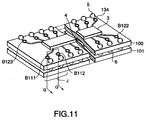
- FIG. 11 is a perspective view showing this type of a stacked module using conductive bumps.
- the stacked module of FIG. 11 is equivalent to a memory circuit of FIG. 10.
- semiconductor chips 3, 4 are respectively chips of DRAMs 80, 81 of FIG. 10.
- the semiconductor chips 3, 4 are mounted facedown on substrates 100, 101.
- the matrix of the substrates 100, 101 is formed by an insulator such as ceramics, glass or the like.
- a conductive bump 5 is mounted on each electrode pad of the substrate 100, a conductive bump 6 is mounted on each electrode pad of the substrate 101, and the respective electrode pads are wired to terminals (not shown) of the semiconductor chips 3, 4. Connection between the substrates 100, 101 is performed through the conductive bumps 6.
- the conductive bumps 5 are served as external terminals at the time of connecting the stacked module of FIG. 11 facedown to a motherboard not shown.
- FIG. 12A shows the upper substrate 100 where the semiconductor chip 3 is mounted
- FIG. 12B shows the lower substrate 101 where the semiconductor chip 4 is mounted
- they are plan views respectively showing the condition before the conductive bumps 5, 6 are mounted.
- Electrode pads 111 to 134 connected to the terminal (not shown) of the semiconductor device 3, on which the conductive bumps 5 are mounted, through hole electrode pads B111 to B134 connected to the electrode pads 111 to 134, and wirings for connecting the respective through hole electrode pads and the terminals of the semiconductor device 3 to each other are formed on the surface of the substrate 100.
- electrode pads 141 to 164 connected to the terminals (not shown) of the semiconductor device 4, on which the conductive bumps 6 of FIG. 11 are mounted, through-hole electrode pads C111 to C134 connected to the electrode pads 141 to 164, and wiring for connecting the respective through-hole electrode pads and the terminals of the semiconductor device 4 to each other are formed on the surface of the substrate 101.
- the reason why the electrode pads on which the conductive bumps 5, 6 are placed are separate from the through-hole electrodes is that the conductive bumps such as solder bumps or the like are prevented from being absorbed in the through-holes.
- the through-hole electrode pads B111 to B134 and C111 to C134 of Figures 12A and 12B are electrically connected to the through-hole electrode pads B111' to B134' and C111' to C134' (only reference numerals, not shown) formed on the back of the substrates 100 and 101 through through-holes.
- the same electrode pads 111' to 134' and 141' to 164' are formed on the back side of the substrates 100 and 101 of the electrode pads 111 to 134 and 141 to 164.
- the electrode pads 111' to 134' on the back side of the substrate 100 are respectively connected to the through-hole electrode pads B111' to B134' on the same back side, and the electrode pads 141' to 164' of the back side of the substrate 101 are respectively connected to the through-hole electrode pads C111' to C134' on the back side.
- the electrode pads and the through-hole electrodes are formed in pair on the surface side and back side of the substrates 100, 101, whereby the electrode patterns are made uniform so as to improve productivity in pattern printing.
- the conductive bumps 6 directly connect the electrode pads 141 to 164 on the surface side of the lower substrate 101 and the electrode pads 111' to 134' on the back side of the upper substrate 100 to each other.
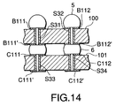
- the condition of the connection is shown in Figures 13 and 14.
- FIG. 13 is a perspective view of a J-part of FIG. 11 to an enlarged scale
- FIG. 14 is a sectional view taken along line G - G of FIG. 11.
- the through electrode pads B111 and B111', B112 and B112', C111 and C111', C112 and C112' are respectively connected to each other by through-hole internal electrodes S31, S32, S33, S34.
- the conductive bumps 6, as shown in FIG. 13, directly connect the electrode pads 111', 112' on the back side of the upper substrate 100 to the electrode pads 141, 142 on the surface side of the lower substrate 101 to each other.
- the connection form of the other electrode pad part is also similar to Figures 13 and 14.
- the respective electrode pads of the substrates 100, 101 are directly connected to each other vertically through the conductive bumps 6.
- the semiconductor devices 3 and 4 are vertically direct-coupled to each other through the conductive bumps 6 to be connected, and mounted facedown on a motherboard not shown through the conductive bumps 5.
- connection for chip select is a wiring part between the RAS terminal of the semiconductor chip 3 and the electrode pads 111, 112, and between the RAS terminal of the semiconductor chip 3 and the electrode pads 141, 142 (through hole electrode pads B111, B112, C111, C112).
- the connection pattern for chip select differs with the substrates of the respective layers.
- a chip select signal is supplied to the electrode pad connected to the RAS of the semiconductor chip 3. At this time, the chip select signal is transmitted to the electrode pad 142, but this is not connected to the RAS, so that the semiconductor device 4 is not selected.
- a chip select signal is supplied to the electrode pad 111 connected to the RAS of the semiconductor chip 4.
- chip select is enabled by changing wiring for chip select at every stage of the substrates. Hence it is necessary to use different substrates in the respective layers in the stacked module.
- a stacked module of the present invention is a stacked module constructed so that substrates on which a semiconductor device having a chip select terminal to be selected according to an external signal is mounted are stacked in N-layer (N is integers from 2 up) and the upper and lower terminals are connected to each other. All of the substrates (1, 2 in FIG. 3 and FIG. 6) have the same wiring structure.
- Each substrate (1 in FIG. 3 and FIG. 6) has N-number of chip select electrodes (B1 and 11, B2 and 12 in FIG. 3 and FIG. 6) arranged adjacent to each other, first chip select electrodes (B1 and 11, C1 and 41 in FIG. 3 and FIG. 6) among N-number of chip select electrodes are connected to the chip select terminal of a mounted semiconductor device (3 in FIG.
- substrates in common can be used all in N-number of layers so as to improve productivity, and even if the upper and lower positional relationship of the substrates is mistaken, there is no obstacle.
- the first chip select electrode is positioned at the most end of N-number of chip select electrodes.
- the other chip select electrodes and the opposite surface side electrodes positioned on the opposite surface side of the adjacent chip select electrode in the direction of the chip select electrode are, to be concrete, connected to each other by conductors (L1, S1, S2 in FIG. 3) arranged in the interior of the substrate.
- a stacked module in which first and second substrates are stacked and upper and lower terminals are connected to each other, is characterized in that the first and second substrates (1, 2 in FIG. 6) have the same wiring structure, the first substrate (1 in FIG. 6) has chip select electrodes (B1 and 11, B2 and 12) arranged adjacent to each other, one side chip select electrodes (B1 and 11) are connected to chip select terminals of a mounted semiconductor device (3 in FIG. 1), the other side chip select electrodes (B2, 12 and S10 in FIG. 6) are pierced through the first substrate to reach the opposite surface side and then connected to the opposite surface side electrodes (11' in FIG.
- the substrate of the present invention includes N-number (N is integers from 2 up) of chip select electrodes arranged adjacent to each other, wherein a first chip select electrode positioned at the most end of the N-number of chip select electrodes is connected to the chip select terminal of the semiconductor device, and the other chip select electrode is connected to the opposite surface side electrode positioned on the opposite surface side of the adjacent chip select electrode in the direction of the first chip select electrode.
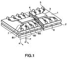
- FIG. 1 is a perspective view, with portions broken away, showing a first embodiment of a stacked module according to the present invention.
- the stacked module of FIG. 1 is equivalent to a memory circuit.
- semiconductor chips 3, 4 are respectively DRAM chips of DRAM 80, 81 of FIG. 10.
- the semiconductor chips 3, 4 are mounted facedown on substrates 1, 2.
- the matrices of the substrates 1, 2 are formed by an insulator such as ceramics or glass.
- a conductive bump 5 such as a solder bump is formed on each electrode pad of the substrate 1
- a conductive bump 6 such as a solder bump or the like is formed on each electrode pad of the substrate 2, and connection between the substrates is performed through the conductive bump 6.
- the conductive bump 5 serves as an external terminal at the time of mounting the stacked module of FIG. 1 facedown on a motherboard not shown.
- the number of external terminals is twenty four.
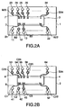
- FIG. 2A shows the upper substrate 1 on which the semiconductor chip 3 is mounted
- FIG. 2B shows the lower substrate 2 on which the semiconductor chip 4 is mounted
- they are plan views respectively showing the condition before the conductive bumps 5, 6 are mounted.
- the substrates 1 and 2 have the same wiring structure.
- FIG. 2A on the surface of the substrate 1, formed are 24 electrode pads 11 to 34 connected to the terminal (not shown) of the semiconductor chip 3, on which the conductive bump 5 of FIG. 1 is mounted, chip select electrode pads B1, B2 connected to the electrode pads 11, 12, through-hole electrode pads B3 to B34 connected to the electrode pads 13 to 34, and wirings 7 for connecting the chip select electrode pads B1, B2, and the through-hole electrode pads B3 to B34 to the respective terminals of the semiconductor chip 3.
- FIG. 2B on the surface of the substrate 2, formed are 24 electrode pads 41 to 64 connected to the terminal (not shown) of the semiconductor chip 4, on which the conductive bump 6 of FIG. 1 is mounted, chip select electrode pads C1, C2 connected to the electrode pads 41, 42, through-hole electrode pads C3 to C34 connected to the electrode pads 43 to 64, and wirings 8 for connecting the chip select electrode pads C1, C2 and the respective through-hole electrode pads to the respective terminals of the semiconductor chip 4.
- the electrode pads 11, 12 (B1, B2) and the electrode pads 41, 42 (C1, C2) of the substrates 1, 2 are the electrode pads for chip select of the semiconductor chips 3, 4, and the other electrode pads 13 to 34 and electrode pads 43 to 64 are connected to terminals other than the chip select terminals and also connected to each other at the time of stacking and packaging.
- the electrode pad 12 (B2) is not connected to the semiconductor chip 3, and the electrode pad 42 (C2) is not connected to the semiconductor chip 4.
- electrode pads for placing the conductive bumps 5, 6 thereon are provided separately from the conductive pads B1 to B34, C1 to C34 is to improve placing of the conductive bumps such as solder bumps or the like.
- the through-hole electrode pads B3 to B34 and the through-hole electrode pads C3 to C34 are electrically connected to through-hole electrode pads B3' to B34' and C3' to C34' (only reference numerals, not shown) formed on the back sides of the substrates 1, 2 through through-holes. Further, the same electrode pads 11' to 34' and 41' to 64' (only reference numerals, not shown) are formed on the back sides of the substrates 1, 2 of the electrode pads 11 to 34 and 41 to 64 on which the conductive bumps 5, 6 are placed.
- the electrode pads 11' to 34' on the back side of the substrate 1 are respectively connected to the chip select electrode pads B1', B2' and the through-hole electrode pads B31' to B34' on the same back side similarly to the surface side, and also the electrode pads 41' to 64' on the back side of the substrate 2 are respectively connected to the chip select electrode pads C1', C2' and the through-hole electrode pads C3' to C34' on the same back side.
- the electrode pads and the through-hole electrodes are formed in pair on the surface sides and the back sides of the substrates 1, 2, whereby the substrates may be used in any layer of the stacked module.
- the conductive bumps 6 respectively connect the electrode pads 41 to 64 of the surface side of the lower substrate 2 and the electrode pads 11' to 34' of the back side of the upper substrate 1 directly to each other. Thus, the connection between the semiconductor chips 3 and 4 through the conductive bumps 6 is enabled.
- FIG. 3 is a perspective view of a part P in FIG. 1 to an enlarged scale
- FIG. 4 is a sectional view taken along line A - A of FIG. 1.
- the chip select electrode pad B2 of the substrate 1 and the electrode pad B1' on the back side of the adjacent chip select electrode pad B1 are connected to each other inside the substrate 1
- the chip select electrode pad C2 of the substrate 2 and the electrode pad C1' on the back side of the adjacent chip select electrode pad C1 are connected to each other inside the substrate 2.
- the chip select electrode pad B2 is connected to the back side electrode pad B1' through a via hole internal electrode S2, an internal conductive layer L1, and a via hole internal electrode S1, and further connected from the electrode pad 11' through the conductive bump 6 to the chip select electrode pad C1.
- the chip select electrode pad C1 is connected to the RAS terminal of the semiconductor device 4 mounted on the lower substrate 2, so that a chip select signal supplied to the chip select electrode pad B2 is supplied to the terminal of RAS of the semiconductor chip 4 to be selected.
- the chip select electrode pad B1 is independent of the electrode pad B2.
- the electrode pad 11 (and B1) of the upper substrate 1 serving as a connecting terminal to a motherboard is connected to the RAS terminal of the semiconductor chip 3, so that chip select for the semiconductor chip 3 is performed by the electrode pad 11.
- chip select electrode pads B1 and B2 are utilized as a terminal for performing chip select for the semiconductor chips 3, 4.
- the same wiring structure as that of the substrate 1 is formed also in the inside of the substrate 2. That is, the chip select electrode C2 is connected to the electrode pad C1' and the electrode pad 41' on the back side through a via hole internal electrode S4, an internal conductive layer L2, and a via hole internal electrode S3.
- the chip select electrode pad C1 is independent of the electrode pad C2.
- the internal wiring of substrate 2 and the electrode pad C2 are unused wiring.
- the substrate 1 includes a two-layer structure of a first layer 1A and a second layer 1B.
- a via hole internal electrode S2 is formed
- a via hole internal electrode S1 is formed, and further an internal conductive layer L1 is formed.
- the substrate 2 is also obtained by forming a first layer 2A and a second layer 2B and stacking the same to each other by the same method as the substrate 1.
- the substrates 1 and 2 have the quite same wiring structure, so that the productivity is high and the yield is improved. Further, even if the positions of the substrates 1, 2 are inverted, the function will not be changed. Hence, it is not necessary to replace a stacked module so as to improve the economical efficiency.
- FIG. 5 is a sectional view showing a second embodiment in which a three-layer substrate is used. However, FIG. 5 shows a section of only a chip select electrode pad part. The wiring structure of the other electrode pads is approximately the same as that in the first embodiment, so the illustration and description are omitted.
- Chip select electrode pads B1 to B3, C1 to C3, D1 to D3 are formed on the surfaces of the substrates 100, 1001, 1002. Further on the back sides thereof, electrode pads B1' to B3', C1' to C3', D1' to D3' are similarly formed.
- the chip select electrode pads B1, C1, and D1 positioned at the most end (left end) are connected to the chip select terminals (RAS terminal of DRAM chip) of the semiconductor chips of the respective layers.
- Conductive bumps 5, 6, 6K are formed on separate electrode pads connected to the electrode pads B1 to B3, C1 to C3, D1 to D3 similarly to the first embodiment.
- the chip select electrode pads B2 and C1 are connected to each other through an internal conductive layer L1, via hole internal electrodes at both ends thereof, and a conductive bump 6, and the chip select electrode pads B3 and D1 are connected to each other through an internal conductive layer L4, via hole internal electrodes at both ends thereof, a conductive bump 6, an electrode pad C2, an internal conductive layer L2 and a conductive bump 6K.
- the respective internal conductive layers L1 to L6 are extended independently of each other toward the chip select electrode pads C1, D1 connected to the chip select terminal (RAS terminal of DRAM chip) of the semiconductor chip.
- the chip select electrode pads B1, B2 and B3 are individually connected to the chip select terminal (RAS terminal) of the semiconductor chip of the substrate of each layer. Moreover, the wiring structure is the same in the respective substrates.
- the internal conductive layers L3, L5, L6 are not used in the case of FIG: 5.
- the substrate is two-layer or three-layer, but in the case of performing chip select for N-number (N is integers) of semiconductor chips, a substrate of N-layer structure is used.
- the number of chip select electrode pads is N equal to that of the semiconductor chips, the respective chip select electrode pads are connected through internal wiring of the substrate and conductive bumps between the upper and lower substrates to the chip select terminal (e.g. RAS terminal of DRAM) of one semiconductor chip to be selected.
- electrodes electrode pads and through-hole internal electrodes vertically piercing the substrates to be connected to each other and N-number of chip select electrode pads are formed on the surfaces of the respective substrates.
- a first chip select electrode pad on the surface of the substrate of the i-th layer (1 ⁇ i ⁇ N, i is integers) from above is connected to a second chip select electrode pad positioned on the opposite surface side of the adjacent chip select electrode pad.
- This connection is performed through an internal conductor (conductive layer).
- the internal conductor is formed toward the direction in which the chip select electrode pad (first chip select electrode pad) connected to the chip select terminal of the semiconductor device is positioned.
- the second chip select electrode pad is connected to a chip select electrode pad on the surface of the substrate of the (i+1)-th layer from above through a conductive bump.
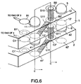
- FIG. 6 is a partial perspective view showing a third embodiment of a stacked module according to the present invention
- FIG. 7 is a sectional view taken along line C - C of FIG. 6.
- back conductive layers L10, L11 are formed on the back sides of the substrates 1, 2 instead of the internal conductive layers L1 and L2 in the embodiment shown in Figures 3 and 4.
- No through-hole and via hole are not formed between the chip select electrode pad B1 (C1) and the electrode pad B1' (C1') on the back side thereof.
- the electrode pads B1' and 11', B2' and 12', C1' and 41', C2' and 42' are not connected with each other.
- the chip select electrode pad B1 is connected to the chip select terminal of the semiconductor chip of the substrate 1.
- the chip select electrode pad B2 is connected through the through-hole internal electrode S10 to the electrode pad B2' on the back side.
- the electrode pad B2' is further connected to the chip select terminal of the semiconductor chip of the substrate 2 through a back conductive layer L10, the back electrode pad 11', the conductive bump 6 and the chip select electrode pad C1.
- the chip select electrode pads B1, B2 function as chip select external terminals of two semiconductor chips similarly to the first embodiment.
- the chip select electrode pad C2 of the substrate 2 is connected through a through-hole internal electrode S11 to an electrode pad C2' on the back side, and further connected from the back conductive layer L11 to the back electrode pad 41', but this connecting path is not used for chip select.
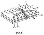
- FIG. 8 is a perspective view showing a fourth embodiment of a stacked module according to the present invention
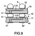
- FIG. 9 is a sectional view taken along line D - D of FIG. 8.
- the stacked module shown in FIG. 8 is so constructed that the same functions as those of the electrode pads B1 to B34 and C1 to C34 shown in FIG. 1 are joined with the electrode pads where the conductive bumps 5, 6 are formed.
- electrode pads 11, 12 on the surface of a substrate 70 on which a semiconductor chip 3 is mounted, and electrode pads 41, 42 on the surface of a substrate 71 on which a semiconductor chip 4 is mounted are chip select electrode pads.
- the other electrode pads are vertically connected to each other through a conductor piercing through the substrates 70, 71.
- the internal conductors L12, L13 play a part instead of the internal conductive layers L1, L2 of FIG. 4.
- connection between the chip select electrode pad and the internal conductive layer is performed by the via hole internal electrode, but in FIG. 9, the via hole is filled up with internal conductors L12, L13.
- no holes such as a via hole and a through-hole are formed in the electrode pads where the conductive bumps 5, 6 are formed, so that the conductive bumps 5, 6 can be formed directly on the electrode pad surface so as to reduce the number of the electrode pads.
- a semiconductor device mounted on a substrate is not limited to a base chip of a semiconductor, but it may be a semiconductor package packaged by resin or ceramics.
- the semiconductor chip 3 is mounted on a surface where the conductive bump 5 is formed in FIG. 1, the semiconductor chip 3 may be mounted on the opposite side to the surface. Further, the chip select electrode pads may be positioned in any place if only they are adjacent to each other. For example, the chip select electrode pads may be formed in the positions of the electrode pads B3, B4.
- first chip select electrodes e.g. B1 and 11, C1 and 42
- the other chip select electrodes B2 and 12 in FIG. 3
- the opposite surface side electrodes B1' and 11' in FIG. 3
- the opposite surface side electrodes and the chip select electrodes (C1 and 41 in FIG. 3) of the substrate (2 in FIG. 3) confronting therewith are connected to each other by the conductive bump (6 in FIG. 3).
- the chip select electrode may be an electrode pad or an electrode pin.
- a conductive bump is not needed.
- a conductive line other than the electrode pin may be all right.
- the other chip select electrodes and the opposite surface side electrodes positioned on the opposite surface side of the adjacent chip select electrode in the direction of the chip select electrode are connected to each other by conductors (e.g. L1, S1, S2 in FIG. 3) arranged in the interior of the substrate.
- the conductors may have any shape.
- the productivity is high and the yield can be improved. Furthermore, even if the positions of the substrates 1, 2 are inverted, the function will not be changed, so that it is not necessary to replace a stacked module and the economical efficiency can be improved.
Abstract
Description
- This invention relates to a packaging structure in which a semiconductor device such as a memory or the like is used, and particularly to a stacked module formed by stacking semiconductor devices and connecting them and substrates used for the stacked module, in which a semiconductor device is mounted on the surface thereof, to be stacked.
- A known packaging method for a semiconductor device is that a semiconductor device is mounted on a substrate, the substrates are stacked in plural layers to construct a stacked module, and the module is mounted on a motherboard. This packaging for a semiconductor device by the stacked module is effective for reducing the packaging area.
- The stacked module using a substrate is effectively utilized for packaging a semiconductor chip such as a semiconductor memory or the like. For example, the case of packaging dynamic RAMs (DRAM) 80, 81 of a memory circuit shown in FIG. 10 will be described. In FIG. 10, the external terminals of the
DRAM terminals - In FIG. 10, terminals other than a chip select terminal for determining which
DRAMs - The stacked module is, for example, as described in Japan Patent Laid-Open No. 8-236694, such that a plurality of substrates (carrier) where a semiconductor chip (LSI chip) is mounted facedown are stacked and connection between the substrates is performed by metallic pins or conductive bumps.
- FIG. 11 is a perspective view showing this type of a stacked module using conductive bumps. The stacked module of FIG. 11 is equivalent to a memory circuit of FIG. 10. In FIG. 11,
semiconductor chips DRAMs - The
semiconductor chips substrates substrates conductive bump 5 is mounted on each electrode pad of thesubstrate 100, aconductive bump 6 is mounted on each electrode pad of thesubstrate 101, and the respective electrode pads are wired to terminals (not shown) of thesemiconductor chips substrates conductive bumps 6. Theconductive bumps 5 are served as external terminals at the time of connecting the stacked module of FIG. 11 facedown to a motherboard not shown. - FIG. 12A shows the
upper substrate 100 where thesemiconductor chip 3 is mounted, FIG. 12B shows thelower substrate 101 where thesemiconductor chip 4 is mounted, and they are plan views respectively showing the condition before theconductive bumps -
Electrode pads 111 to 134 connected to the terminal (not shown) of thesemiconductor device 3, on which theconductive bumps 5 are mounted, through hole electrode pads B111 to B134 connected to theelectrode pads 111 to 134, and wirings for connecting the respective through hole electrode pads and the terminals of thesemiconductor device 3 to each other are formed on the surface of thesubstrate 100. - On the other hand,
electrode pads 141 to 164 connected to the terminals (not shown) of thesemiconductor device 4, on which theconductive bumps 6 of FIG. 11 are mounted, through-hole electrode pads C111 to C134 connected to theelectrode pads 141 to 164, and wiring for connecting the respective through-hole electrode pads and the terminals of thesemiconductor device 4 to each other are formed on the surface of thesubstrate 101. The reason why the electrode pads on which theconductive bumps - The through-hole electrode pads B111 to B134 and C111 to C134 of Figures 12A and 12B are electrically connected to the through-hole electrode pads B111' to B134' and C111' to C134' (only reference numerals, not shown) formed on the back of the
substrates substrates electrode pads 111 to 134 and 141 to 164. - The electrode pads 111' to 134' on the back side of the
substrate 100 are respectively connected to the through-hole electrode pads B111' to B134' on the same back side, and the electrode pads 141' to 164' of the back side of thesubstrate 101 are respectively connected to the through-hole electrode pads C111' to C134' on the back side. - Thus, the electrode pads and the through-hole electrodes are formed in pair on the surface side and back side of the
substrates - The
conductive bumps 6 directly connect theelectrode pads 141 to 164 on the surface side of thelower substrate 101 and the electrode pads 111' to 134' on the back side of theupper substrate 100 to each other. The condition of the connection is shown in Figures 13 and 14. - Figures 13 is a perspective view of a J-part of FIG. 11 to an enlarged scale, and FIG. 14 is a sectional view taken along line G - G of FIG. 11. As shown in Figures 13 and 14, the through electrode pads B111 and B111', B112 and B112', C111 and C111', C112 and C112' are respectively connected to each other by through-hole internal electrodes S31, S32, S33, S34. The
conductive bumps 6, as shown in FIG. 13, directly connect the electrode pads 111', 112' on the back side of theupper substrate 100 to theelectrode pads lower substrate 101 to each other. The connection form of the other electrode pad part is also similar to Figures 13 and 14. As the result, the respective electrode pads of thesubstrates conductive bumps 6. - As described above, the
semiconductor devices conductive bumps 6 to be connected, and mounted facedown on a motherboard not shown through theconductive bumps 5. - Again in Figures 12A and 12B, connection for chip select is a wiring part between the RAS terminal of the
semiconductor chip 3 and theelectrode pads semiconductor chip 3 and theelectrode pads 141, 142 (through hole electrode pads B111, B112, C111, C112). However, the connection pattern for chip select differs with the substrates of the respective layers. - In the case of selecting the
semiconductor chip 3 at the time of reading and writing data, as shown in FIG. 12A, a chip select signal is supplied to the electrode pad connected to the RAS of thesemiconductor chip 3. At this time, the chip select signal is transmitted to theelectrode pad 142, but this is not connected to the RAS, so that thesemiconductor device 4 is not selected. On the other hand, in the case of selecting thesemiconductor chip 4 at the time of reading and writing, a chip select signal is supplied to theelectrode pad 111 connected to the RAS of thesemiconductor chip 4. Thus, selection from thesemiconductor devices electrode pads substrate 100. - In the described conventional stacked module, chip select is enabled by changing wiring for chip select at every stage of the substrates. Hence it is necessary to use different substrates in the respective layers in the stacked module.
- That is, it is necessary to manufacture substrates with plural wiring patterns, so that productivity is low and the yield is bad. Further, when the arrangement of substrates in the stacked module is wrong, it is necessary to replace the whole of the stacked module.
- Accordingly it is the object of the invention to provide a substrate and a stacked module in which the described problems are solved by making the wiring part for chip select in common.
- A stacked module of the present invention is a stacked module constructed so that substrates on which a semiconductor device having a chip select terminal to be selected according to an external signal is mounted are stacked in N-layer (N is integers from 2 up) and the upper and lower terminals are connected to each other. All of the substrates (1, 2 in FIG. 3 and FIG. 6) have the same wiring structure. Each substrate (1 in FIG. 3 and FIG. 6) has N-number of chip select electrodes (B1 and 11, B2 and 12 in FIG. 3 and FIG. 6) arranged adjacent to each other, first chip select electrodes (B1 and 11, C1 and 41 in FIG. 3 and FIG. 6) among N-number of chip select electrodes are connected to the chip select terminal of a mounted semiconductor device (3 in FIG. 1), and the other chip select electrodes (B2 and 12 of FIG. 3 and FIG. 6) are connected to opposite surface side electrodes (B1' and 11' in FIG. 3, 11' in FIG. 6) positioned on the opposite surface side of the adjacent chip select electrode in the direction of the first chip select electrode. The opposite surface side electrodes and the chip select electrodes (C1 and 41 in FIG. 3 and FIG. 6) of the substrate (2 in FIG. 3 and FIG. 6) confronting therewith are connected to each other by conductive bumps (6 in FIG. 3 and FIG. 6).
- Thus, substrates in common can be used all in N-number of layers so as to improve productivity, and even if the upper and lower positional relationship of the substrates is mistaken, there is no obstacle.
- In the described invention, to simplify wiring, the first chip select electrode is positioned at the most end of N-number of chip select electrodes.
- The other chip select electrodes and the opposite surface side electrodes positioned on the opposite surface side of the adjacent chip select electrode in the direction of the chip select electrode are, to be concrete, connected to each other by conductors (L1, S1, S2 in FIG. 3) arranged in the interior of the substrate.
- According to the present invention, a stacked module, in which first and second substrates are stacked and upper and lower terminals are connected to each other, is characterized in that the first and second substrates (1, 2 in FIG. 6) have the same wiring structure, the first substrate (1 in FIG. 6) has chip select electrodes (B1 and 11, B2 and 12) arranged adjacent to each other, one side chip select electrodes (B1 and 11) are connected to chip select terminals of a mounted semiconductor device (3 in FIG. 1), the other side chip select electrodes (B2, 12 and S10 in FIG. 6) are pierced through the first substrate to reach the opposite surface side and then connected to the opposite surface side electrodes (11' in FIG. 6) positioned on the opposite surface side of one side chip select electrodes through a conductor (L10 in FIG. 6), and the opposite surface side electrodes and the chip select electrodes (C1 and 41 in FIG. 6) of the second substrate (2 in FIG. 6) confronting therewith are connected to each other by a conductive bump (6 in FIG. 6).
- As a conductor is not formed in the interior of the substrate in the described stacked module, it is not necessary to construct the substrate in multi-layer, resulting in the advantage that the substrate can be manufactured at a low cost and the thickness is not increased.
- The substrate of the present invention includes N-number (N is integers from 2 up) of chip select electrodes arranged adjacent to each other, wherein a first chip select electrode positioned at the most end of the N-number of chip select electrodes is connected to the chip select terminal of the semiconductor device, and the other chip select electrode is connected to the opposite surface side electrode positioned on the opposite surface side of the adjacent chip select electrode in the direction of the first chip select electrode.
-
- FIG. 1 is a perspective view, with portions broken away, showing a first embodiment of a stacked module according to the present invention;
- FIG. 2A is a plan view showing an upper substrate of the stacked module shown in FIG. 1; FIG. 2B is a plan view showing a lower substrate;
- FIG. 3 is a perspective view of a part P in FIG. 1 to an enlarged scale;
- FIG. 4 is a sectional view taken along line A - A of FIG. 1;
- FIG. 5 is a partial sectional view showing a second embodiment of a stacked module according to the present invention;
- FIG. 6 is a partial perspective view showing a third embodiment of a stacked module according to the present invention;
- FIG. 7 is a sectional view taken along line C - C of FIG. 6;
- FIG. 8 is a perspective view, with portions broken away, showing a fourth embodiment of a stacked module according to the present invention;
- FIG. 9 is a sectional view taken along line D - D of FIG. 8;
- FIG. 10 is a circuit diagram of a memory circuit using DRAM;
- FIG. 11 is a perspective view, with portions broken away, showing the conventional stacked module;
- FIG. 12A is a plan view showing an upper substrate of the stacked module shown in FIG. 11; FIG. 12B is a plan view showing a lower substrate;
- FIG. 13 is a perspective view of a part J in FIG. 11 to an enlarged scale; and
- FIG. 14 is a sectional view taken along line G - G of FIG. 11.
-
- FIG. 1 is a perspective view, with portions broken away, showing a first embodiment of a stacked module according to the present invention. The stacked module of FIG. 1 is equivalent to a memory circuit. In FIG. 1,
semiconductor chips DRAM - The semiconductor chips 3, 4 are mounted facedown on
substrates substrates conductive bump 5 such as a solder bump is formed on each electrode pad of thesubstrate 1, aconductive bump 6 such as a solder bump or the like is formed on each electrode pad of thesubstrate 2, and connection between the substrates is performed through theconductive bump 6. Theconductive bump 5 serves as an external terminal at the time of mounting the stacked module of FIG. 1 facedown on a motherboard not shown. The number of external terminals is twenty four. - FIG. 2A shows the
upper substrate 1 on which thesemiconductor chip 3 is mounted, FIG. 2B shows thelower substrate 2 on which thesemiconductor chip 4 is mounted, and they are plan views respectively showing the condition before theconductive bumps substrates - In FIG. 2A, on the surface of the
substrate 1, formed are 24electrode pads 11 to 34 connected to the terminal (not shown) of thesemiconductor chip 3, on which theconductive bump 5 of FIG. 1 is mounted, chip select electrode pads B1, B2 connected to theelectrode pads electrode pads 13 to 34, and wirings 7 for connecting the chip select electrode pads B1, B2, and the through-hole electrode pads B3 to B34 to the respective terminals of thesemiconductor chip 3. - On the other hand, in FIG. 2B, on the surface of the
substrate 2, formed are 24electrode pads 41 to 64 connected to the terminal (not shown) of thesemiconductor chip 4, on which theconductive bump 6 of FIG. 1 is mounted, chip select electrode pads C1, C2 connected to theelectrode pads electrode pads 43 to 64, and wirings 8 for connecting the chip select electrode pads C1, C2 and the respective through-hole electrode pads to the respective terminals of thesemiconductor chip 4. - The
electrode pads 11, 12 (B1, B2) and theelectrode pads 41, 42 (C1, C2) of thesubstrates semiconductor chips other electrode pads 13 to 34 andelectrode pads 43 to 64 are connected to terminals other than the chip select terminals and also connected to each other at the time of stacking and packaging. The electrode pad 12 (B2) is not connected to thesemiconductor chip 3, and the electrode pad 42 (C2) is not connected to thesemiconductor chip 4. - The reason why electrode pads for placing the
conductive bumps - In Figures 2A and 2B, the through-hole electrode pads B3 to B34 and the through-hole electrode pads C3 to C34 are electrically connected to through-hole electrode pads B3' to B34' and C3' to C34' (only reference numerals, not shown) formed on the back sides of the
substrates same electrode pads 11' to 34' and 41' to 64' (only reference numerals, not shown) are formed on the back sides of thesubstrates electrode pads 11 to 34 and 41 to 64 on which theconductive bumps - The
electrode pads 11' to 34' on the back side of thesubstrate 1 are respectively connected to the chip select electrode pads B1', B2' and the through-hole electrode pads B31' to B34' on the same back side similarly to the surface side, and also the electrode pads 41' to 64' on the back side of thesubstrate 2 are respectively connected to the chip select electrode pads C1', C2' and the through-hole electrode pads C3' to C34' on the same back side. Thus, the electrode pads and the through-hole electrodes are formed in pair on the surface sides and the back sides of thesubstrates - The
conductive bumps 6 respectively connect theelectrode pads 41 to 64 of the surface side of thelower substrate 2 and theelectrode pads 11' to 34' of the back side of theupper substrate 1 directly to each other. Thus, the connection between thesemiconductor chips conductive bumps 6 is enabled. - In the present embodiment, to let the
substrates semiconductor chips semiconductor chips - FIG. 3 is a perspective view of a part P in FIG. 1 to an enlarged scale, and FIG. 4 is a sectional view taken along line A - A of FIG. 1. As shown in Figures 3 and 4, the chip select electrode pad B2 of the
substrate 1 and the electrode pad B1' on the back side of the adjacent chip select electrode pad B1 are connected to each other inside thesubstrate 1, and the chip select electrode pad C2 of thesubstrate 2 and the electrode pad C1' on the back side of the adjacent chip select electrode pad C1 are connected to each other inside thesubstrate 2. - To be more in detail, in FIG. 3, the chip select electrode pad B2 is connected to the back side electrode pad B1' through a via hole internal electrode S2, an internal conductive layer L1, and a via hole internal electrode S1, and further connected from the
electrode pad 11' through theconductive bump 6 to the chip select electrode pad C1. The chip select electrode pad C1 is connected to the RAS terminal of thesemiconductor device 4 mounted on thelower substrate 2, so that a chip select signal supplied to the chip select electrode pad B2 is supplied to the terminal of RAS of thesemiconductor chip 4 to be selected. - The chip select electrode pad B1 is independent of the electrode pad B2.
- Hence, the electrode pad 11 (and B1) of the
upper substrate 1 serving as a connecting terminal to a motherboard is connected to the RAS terminal of thesemiconductor chip 3, so that chip select for thesemiconductor chip 3 is performed by theelectrode pad 11. - Thus, the chip select electrode pads B1 and B2 (
electrode pads 11 and 12) are utilized as a terminal for performing chip select for thesemiconductor chips - The same wiring structure as that of the
substrate 1 is formed also in the inside of thesubstrate 2. That is, the chip select electrode C2 is connected to the electrode pad C1' and the electrode pad 41' on the back side through a via hole internal electrode S4, an internal conductive layer L2, and a via hole internal electrode S3. The chip select electrode pad C1 is independent of the electrode pad C2. However, in the first embodiment, the internal wiring ofsubstrate 2 and the electrode pad C2 are unused wiring. - As shown in FIG. 4, the
substrate 1 includes a two-layer structure of afirst layer 1A and asecond layer 1B. In thefirst layer 1A, after boring, a via hole internal electrode S2 is formed, and in thesecond layer 1B, after boring, a via hole internal electrode S1 is formed, and further an internal conductive layer L1 is formed. - The
substrate 2 is also obtained by forming a first layer 2A and asecond layer 2B and stacking the same to each other by the same method as thesubstrate 1. - As described above, in the first embodiment, the
substrates substrates - FIG. 5 is a sectional view showing a second embodiment in which a three-layer substrate is used. However, FIG. 5 shows a section of only a chip select electrode pad part. The wiring structure of the other electrode pads is approximately the same as that in the first embodiment, so the illustration and description are omitted.
- In the FIG. 5, all of
substrates substrates - Among the above chip select electrode pads, the chip select electrode pads B1, C1, and D1 positioned at the most end (left end) are connected to the chip select terminals (RAS terminal of DRAM chip) of the semiconductor chips of the respective layers.
Conductive bumps - The chip select electrode pads B2 and C1 are connected to each other through an internal conductive layer L1, via hole internal electrodes at both ends thereof, and a
conductive bump 6, and the chip select electrode pads B3 and D1 are connected to each other through an internal conductive layer L4, via hole internal electrodes at both ends thereof, aconductive bump 6, an electrode pad C2, an internal conductive layer L2 and aconductive bump 6K. - The respective internal conductive layers L1 to L6 are extended independently of each other toward the chip select electrode pads C1, D1 connected to the chip select terminal (RAS terminal of DRAM chip) of the semiconductor chip.
- Accordingly, the chip select electrode pads B1, B2 and B3 are individually connected to the chip select terminal (RAS terminal) of the semiconductor chip of the substrate of each layer. Moreover, the wiring structure is the same in the respective substrates. The internal conductive layers L3, L5, L6 are not used in the case of FIG: 5.
- In the first and second embodiments of stacked modules, the substrate is two-layer or three-layer, but in the case of performing chip select for N-number (N is integers) of semiconductor chips, a substrate of N-layer structure is used. In this case, the number of chip select electrode pads is N equal to that of the semiconductor chips, the respective chip select electrode pads are connected through internal wiring of the substrate and conductive bumps between the upper and lower substrates to the chip select terminal (e.g. RAS terminal of DRAM) of one semiconductor chip to be selected.
- To be concrete, in a stacked module formed by stacking N-layers, electrodes (electrode pads and through-hole internal electrodes) vertically piercing the substrates to be connected to each other and N-number of chip select electrode pads are formed on the surfaces of the respective substrates. A first chip select electrode pad on the surface of the substrate of the i-th layer (1 ≦ i <N, i is integers) from above is connected to a second chip select electrode pad positioned on the opposite surface side of the adjacent chip select electrode pad. This connection is performed through an internal conductor (conductive layer). In this case, the internal conductor is formed toward the direction in which the chip select electrode pad (first chip select electrode pad) connected to the chip select terminal of the semiconductor device is positioned. Further, the second chip select electrode pad is connected to a chip select electrode pad on the surface of the substrate of the (i+1)-th layer from above through a conductive bump. Thus, the substrates of the same wiring structure can be used for N-layers.
- FIG. 6 is a partial perspective view showing a third embodiment of a stacked module according to the present invention, and FIG. 7 is a sectional view taken along line C - C of FIG. 6. In the present embodiment, back conductive layers L10, L11 are formed on the back sides of the
substrates - No through-hole and via hole are not formed between the chip select electrode pad B1 (C1) and the electrode pad B1' (C1') on the back side thereof. The electrode pads B1' and 11', B2' and 12', C1' and 41', C2' and 42' are not connected with each other.
- The chip select electrode pad B1 is connected to the chip select terminal of the semiconductor chip of the
substrate 1. The chip select electrode pad B2 is connected through the through-hole internal electrode S10 to the electrode pad B2' on the back side. The electrode pad B2' is further connected to the chip select terminal of the semiconductor chip of thesubstrate 2 through a back conductive layer L10, theback electrode pad 11', theconductive bump 6 and the chip select electrode pad C1. - Accordingly, the chip select electrode pads B1, B2 function as chip select external terminals of two semiconductor chips similarly to the first embodiment.
- The chip select electrode pad C2 of the
substrate 2 is connected through a through-hole internal electrode S11 to an electrode pad C2' on the back side, and further connected from the back conductive layer L11 to the back electrode pad 41', but this connecting path is not used for chip select. - In the case of stacked modules shown in Figures 6 and 7, it is possible to connect three or more layers of substrates to each other. In this stacked module, a conductive layer is not formed in the substrate, so it is not necessary to form a substrate of a multi-layer structure, resulting in the advantage that the substrate can be formed at a low cost and is not increased in thickness.
- FIG. 8 is a perspective view showing a fourth embodiment of a stacked module according to the present invention, and FIG. 9 is a sectional view taken along line D - D of FIG. 8. The stacked module shown in FIG. 8 is so constructed that the same functions as those of the electrode pads B1 to B34 and C1 to C34 shown in FIG. 1 are joined with the electrode pads where the
conductive bumps - In FIG. 9,
electrode pads substrate 70 on which asemiconductor chip 3 is mounted, andelectrode pads substrate 71 on which asemiconductor chip 4 is mounted are chip select electrode pads. The other electrode pads are vertically connected to each other through a conductor piercing through thesubstrates - The internal conductors L12, L13 play a part instead of the internal conductive layers L1, L2 of FIG. 4. In FIG. 4, connection between the chip select electrode pad and the internal conductive layer is performed by the via hole internal electrode, but in FIG. 9, the via hole is filled up with internal conductors L12, L13.
- In the present embodiment, no holes such as a via hole and a through-hole are formed in the electrode pads where the
conductive bumps conductive bumps - The stacked module of the present invention is not limited to the described embodiments. For example, a semiconductor device mounted on a substrate is not limited to a base chip of a semiconductor, but it may be a semiconductor package packaged by resin or ceramics.
- Though the
semiconductor chip 3 is mounted on a surface where theconductive bump 5 is formed in FIG. 1, thesemiconductor chip 3 may be mounted on the opposite side to the surface. Further, the chip select electrode pads may be positioned in any place if only they are adjacent to each other. For example, the chip select electrode pads may be formed in the positions of the electrode pads B3, B4. - In the embodiments of the present invention, it will be sufficient that first chip select electrodes (e.g. B1 and 11, C1 and 42) positioned at the most end among N-number of chip select electrodes are connected to chip select terminals of the mounted semiconductor device (3 in FIG. 1), and the other chip select electrodes (B2 and 12 in FIG. 3) are the opposite surface side electrodes (B1' and 11' in FIG. 3) positioned on the opposite surface side of the adjacent chip select electrode confronting with the first chip select electrodes. Further it will be sufficient that the opposite surface side electrodes and the chip select electrodes (C1 and 41 in FIG. 3) of the substrate (2 in FIG. 3) confronting therewith are connected to each other by the conductive bump (6 in FIG. 3).
- In this case, the chip select electrode may be an electrode pad or an electrode pin. In the case of the electrode pin, a conductive bump is not needed. Furthermore, a conductive line other than the electrode pin may be all right.
- In the embodiments of the present invention, the other chip select electrodes and the opposite surface side electrodes positioned on the opposite surface side of the adjacent chip select electrode in the direction of the chip select electrode are connected to each other by conductors (e.g. L1, S1, S2 in FIG. 3) arranged in the interior of the substrate. The conductors may have any shape.
- According to the present invention, as described above, it will be apparent that as all of the substrates have the quite same wiring structure, the productivity is high and the yield can be improved. Furthermore, even if the positions of the
substrates
Claims (11)
- A stacked module, in a stacked module formed by stacking N-layer (N is integers from 2 up) of substrates (1, 2) where a semiconductor device (3, 4) having a chip select terminal to be selected according to an external signal is mounted and connecting upper and lower terminals to each other, characterized in thatall of said substrates (1, 2) have the same wiring structure,said substrates (1, 2) include N-number of chip select electrodes (B1, B2, C1, C2) arranged adjacent to each other, a first chip select electrode (B1, C1) among N-number of said chip select electrodes (B1, B2, C1, C2) is connected to a chip select terminal of said mounted semiconductor device (3, 4), the other chip select electrodes (B2, C2) are connected to opposite surface side electrodes (B1', C1') positioned on an opposite surface side of an adjacent chip select electrode in a direction of said first chip select electrode (B1, C1), andsaid opposite surface side electrodes (B1', C1') and said chip select electrodes (C1) of said substrate (2) confronted therewith are connected to each other.
- The stacked module as claimed in claim 1, wherein said first chip select electrode (B1, C1) is an electrode positioned at the most end among N-number of said chip select electrodes (B1, B2, C1, C2).
- The stacked module as claimed in claim 2, wherein said other chip select electrodes (B2, C2) and said opposite surface side electrodes (B1', C1') are connected to each other by conductors arranged in an interior of said substrates (1, 2).
- The stacked module as claimed in claim 2, wherein said other chip select electrodes (B2, C2) and said opposite surface side electrodes (B1', C1') are connected to each other by conductors formed on said opposite surface side of said substrates (1, 2).
- The stacked module as claimed in claim 2, wherein said opposite surface side electrodes (B1', C1') and said chip select electrodes (C1) of said substrate (2) confronted therewith are connected to each other by conductive bumps (6).
- The stacked module as claimed in claim 1, wherein said substrates (1, 2) include electrodes connected to terminals other than said chip select terminals of said semiconductor device and vertically pierced through said substrates (1, 2), and said piercing electrodes are connected to each other through conductive bumps between the respective substrates.
- A stacked module, in a stacked module formed by stacking first and second substrates (1, 2) where a semiconductor device (3, 4) having a chip select terminal to be selected according to an external signal is mounted and connecting upper and lower terminals to each other, characterized in thatsaid first and second substrates (1, 2) have the same wiring structure,said first substrate (1) includes chip select electrodes (B1, B2) arranged adjacent to each other, one chip select electrode (B1) is connected to a chip select terminal of said semiconductor device (3), the other chip select electrode (B2) is pierced through said first substrate (1) to reach an opposite surface side and then connected to an opposite surface side electrode (B1') positioned on the opposite surface side of said one chip select electrode (B1) through a conductor, andsaid opposite surface side electrode (B1') and said chip select electrode (C1) of said second substrate (2) confronted therewith are connected to each other by a conductive bump (6).
- A substrate for a stacked module formed by stacking N-layer (N is integers from 2 up) of substrates (1, 2) on which a semiconductor device (3, 4) having chip select terminals to be selected according to an external signal is mounted,
characterized in that said substrate (1, 2) includes N-number (N is integers from 2 up) of chip select electrodes (B1, B2, C1, C2), a first chip select electrode (B1, C1) among N-number of said chip select electrodes (B1, B2, C1, C2) is connected to the chip select terminal of said semiconductor device (3, 4), and the other chip select electrodes (B2, C2) are connected to opposite surface side electrodes (B1', C1') positioned on an opposite surface side of an adjacent chip select electrode in a direction of said first chip select electrode (B1, C1). - The substrate claimed in claim 8, wherein said first chip select electrode (B1, C1) is an electrode positioned at the most end among N-number of said chip select electrodes (B1, B2, C1, C2).
- The stacked module claimed in claim 8, wherein said other chip select electrodes (B2, C2) and said opposite surface side electrodes (B1', C1') are connected to each other by conductors arranged in the interior of said substrates (1, 2).
- The stacked module claimed in claim 8, wherein said other chip select electrodes (B2, C2) and said opposite surface side electrodes (B1', C1') are connected to each other by conductors formed on said opposite surface side of said substrates (1, 2).
Applications Claiming Priority (3)
| Application Number | Priority Date | Filing Date | Title |
|---|---|---|---|
| JP298909/97 | 1997-10-30 | ||
| JP29890997 | 1997-10-30 | ||
| JP9298909A JP2870530B1 (en) | 1997-10-30 | 1997-10-30 | Stack module interposer and stack module |
Publications (2)
| Publication Number | Publication Date |
|---|---|
| EP0915516A2 true EP0915516A2 (en) | 1999-05-12 |
| EP0915516A3 EP0915516A3 (en) | 2004-01-02 |
Family
ID=17865748
Family Applications (1)
| Application Number | Title | Priority Date | Filing Date |
|---|---|---|---|
| EP98120397A Withdrawn EP0915516A3 (en) | 1997-10-30 | 1998-10-28 | Substrate for stacked module and stacked module |
Country Status (5)
| Country | Link |
|---|---|
| US (1) | US5995379A (en) |
| EP (1) | EP0915516A3 (en) |
| JP (1) | JP2870530B1 (en) |
| KR (1) | KR100298282B1 (en) |
| TW (1) | TW405247B (en) |
Cited By (4)
| Publication number | Priority date | Publication date | Assignee | Title |
|---|---|---|---|---|
| DE10049551A1 (en) * | 1999-10-26 | 2001-05-03 | Sharp Kk | Connection structure for stackable semiconductor chips e.g. LSI chips, has bump electrode and contact spot electrode at top and bottom faces of chip, and connecting electrodes at front and rear of chip |
| DE10134648A1 (en) * | 2001-07-20 | 2002-10-10 | Infineon Technologies Ag | Stacked electronic component device has perpendicular pins providing mechanical and electrical connections between stacked electronic components |
| EP1288968A2 (en) * | 2001-07-24 | 2003-03-05 | Hewlett-Packard Company | Solid state memory |
| EP1685600A1 (en) * | 2003-09-05 | 2006-08-02 | Sanmina-SCI Corporation | Stackable electronic assembly |
Families Citing this family (72)
| Publication number | Priority date | Publication date | Assignee | Title |
|---|---|---|---|---|
| US6002177A (en) * | 1995-12-27 | 1999-12-14 | International Business Machines Corporation | High density integrated circuit packaging with chip stacking and via interconnections |
| JP3268740B2 (en) * | 1997-08-20 | 2002-03-25 | 株式会社東芝 | ASIC design / manufacturing method, standard cell, embedded array, and multi-chip package |
| JP3727172B2 (en) * | 1998-06-09 | 2005-12-14 | 沖電気工業株式会社 | Semiconductor device |
| JP3563604B2 (en) * | 1998-07-29 | 2004-09-08 | 株式会社東芝 | Multi-chip semiconductor device and memory card |
| US6504241B1 (en) * | 1998-10-15 | 2003-01-07 | Sony Corporation | Stackable semiconductor device and method for manufacturing the same |
| US6122187A (en) | 1998-11-23 | 2000-09-19 | Micron Technology, Inc. | Stacked integrated circuits |
| KR100319608B1 (en) | 1999-03-09 | 2002-01-05 | 김영환 | A stacked semiconductor package and the fabricating method thereof |
| JP2000277944A (en) * | 1999-03-24 | 2000-10-06 | Ando Electric Co Ltd | Board and method for expansion |
| JP3213292B2 (en) * | 1999-07-12 | 2001-10-02 | ソニーケミカル株式会社 | Multilayer board and module |
| JP4051531B2 (en) | 1999-07-22 | 2008-02-27 | セイコーエプソン株式会社 | Semiconductor device and manufacturing method thereof, circuit board, and electronic apparatus |
| KR100343453B1 (en) * | 1999-10-28 | 2002-07-11 | 박종섭 | Mult-laminated type memory module |
| US6404660B1 (en) * | 1999-12-23 | 2002-06-11 | Rambus, Inc. | Semiconductor package with a controlled impedance bus and method of forming same |
| DE10009171B4 (en) * | 2000-02-26 | 2005-08-11 | Robert Bosch Gmbh | Power converter and its manufacturing process |
| JP3779524B2 (en) * | 2000-04-20 | 2006-05-31 | 株式会社東芝 | Multi-chip semiconductor device and memory card |
| DE10044148A1 (en) * | 2000-09-06 | 2002-03-21 | Infineon Technologies Ag | Electronic component with stacked components and process for its manufacture |
| JP3405456B2 (en) * | 2000-09-11 | 2003-05-12 | 沖電気工業株式会社 | Semiconductor device, method of manufacturing semiconductor device, stack type semiconductor device, and method of manufacturing stack type semiconductor device |
| US7444575B2 (en) * | 2000-09-21 | 2008-10-28 | Inapac Technology, Inc. | Architecture and method for testing of an integrated circuit device |
| US7240254B2 (en) * | 2000-09-21 | 2007-07-03 | Inapac Technology, Inc | Multiple power levels for a chip within a multi-chip semiconductor package |
| US6812726B1 (en) * | 2002-11-27 | 2004-11-02 | Inapac Technology, Inc. | Entering test mode and accessing of a packaged semiconductor device |
| JP3934867B2 (en) * | 2000-09-29 | 2007-06-20 | 株式会社東芝 | Nonvolatile semiconductor memory device and nonvolatile semiconductor memory system |
| US6653572B2 (en) * | 2001-02-07 | 2003-11-25 | The Furukawa Electric Co., Ltd. | Multilayer circuit board |
| KR100364635B1 (en) * | 2001-02-09 | 2002-12-16 | 삼성전자 주식회사 | Chip-Level Three-Dimensional Multi-Chip Package Having Chip Selection Pad Formed On Chip-Level And Making Method Therefor |
| US6469375B2 (en) * | 2001-02-28 | 2002-10-22 | William F. Beausoleil | High bandwidth 3D memory packaging technique |
| US7610447B2 (en) * | 2001-02-28 | 2009-10-27 | Rambus Inc. | Upgradable memory system with reconfigurable interconnect |
| US6889304B2 (en) | 2001-02-28 | 2005-05-03 | Rambus Inc. | Memory device supporting a dynamically configurable core organization |
| DE10125025A1 (en) * | 2001-05-22 | 2002-12-12 | Infineon Technologies Ag | Circuit board for memory components has contacts on first surface associated with memory component contacts, contact spheres connecting component and board contacts, conducting tracks |
| JP4109839B2 (en) * | 2001-06-01 | 2008-07-02 | 株式会社東芝 | Semiconductor device |
| US6914786B1 (en) * | 2001-06-14 | 2005-07-05 | Lsi Logic Corporation | Converter device |
| JP2003060053A (en) * | 2001-08-10 | 2003-02-28 | Fujitsu Ltd | Semiconductor chip, semiconductor integrated circuit device comprising it and method for selecting semiconductor chip |
| JP2003100947A (en) | 2001-09-20 | 2003-04-04 | Mitsubishi Electric Corp | Semiconductor device and semiconductor device module |
| US8166361B2 (en) | 2001-09-28 | 2012-04-24 | Rambus Inc. | Integrated circuit testing module configured for set-up and hold time testing |
| US8001439B2 (en) | 2001-09-28 | 2011-08-16 | Rambus Inc. | Integrated circuit testing module including signal shaping interface |
| US8286046B2 (en) | 2001-09-28 | 2012-10-09 | Rambus Inc. | Integrated circuit testing module including signal shaping interface |
| US7313740B2 (en) * | 2002-07-25 | 2007-12-25 | Inapac Technology, Inc. | Internally generating patterns for testing in an integrated circuit device |
| US6611052B2 (en) * | 2001-11-16 | 2003-08-26 | Micron Technology, Inc. | Wafer level stackable semiconductor package |
| US7046522B2 (en) * | 2002-03-21 | 2006-05-16 | Raymond Jit-Hung Sung | Method for scalable architectures in stackable three-dimensional integrated circuits and electronics |
| US6542393B1 (en) | 2002-04-24 | 2003-04-01 | Ma Laboratories, Inc. | Dual-bank memory module with stacked DRAM chips having a concave-shaped re-route PCB in-between |
| US6891447B2 (en) * | 2002-07-12 | 2005-05-10 | Massachusetts Institute Of Technology | Electromagnetic coupling connector for three-dimensional electronic circuits |
| US8063650B2 (en) | 2002-11-27 | 2011-11-22 | Rambus Inc. | Testing fuse configurations in semiconductor devices |
| US6809269B2 (en) * | 2002-12-19 | 2004-10-26 | Endicott Interconnect Technologies, Inc. | Circuitized substrate assembly and method of making same |
| US7183643B2 (en) | 2003-11-04 | 2007-02-27 | Tessera, Inc. | Stacked packages and systems incorporating the same |
| WO2005086216A1 (en) * | 2004-03-09 | 2005-09-15 | Japan Science And Technology Agency | Semiconductor element and semiconductor element manufacturing method |
| US20060206745A1 (en) * | 2005-03-11 | 2006-09-14 | Advanced Micro Devices, Inc. | Automatic resource assignment in devices having stacked modules |
| US7251160B2 (en) * | 2005-03-16 | 2007-07-31 | Sandisk Corporation | Non-volatile memory and method with power-saving read and program-verify operations |
| JP4577688B2 (en) * | 2005-05-09 | 2010-11-10 | エルピーダメモリ株式会社 | Semiconductor chip selection method, semiconductor chip, and semiconductor integrated circuit device |
| US7095602B1 (en) | 2005-06-29 | 2006-08-22 | Murata Manufacturing Co., Ltd. | Ceramic structure and nonreciprocal circuit device |
| US7826243B2 (en) * | 2005-12-29 | 2010-11-02 | Bitmicro Networks, Inc. | Multiple chip module and package stacking for storage devices |
| JP4753725B2 (en) * | 2006-01-20 | 2011-08-24 | エルピーダメモリ株式会社 | Multilayer semiconductor device |
| US7701045B2 (en) * | 2006-04-11 | 2010-04-20 | Rambus Inc. | Point-to-point connection topology for stacked devices |
| US7506098B2 (en) * | 2006-06-08 | 2009-03-17 | Bitmicro Networks, Inc. | Optimized placement policy for solid state storage devices |
| US7952184B2 (en) * | 2006-08-31 | 2011-05-31 | Micron Technology, Inc. | Distributed semiconductor device methods, apparatus, and systems |
| KR100827724B1 (en) | 2006-09-12 | 2008-05-07 | 엠텍비젼 주식회사 | System in package having stacking structure of wafer level package and manufacturing method thereof |
| US7781927B2 (en) * | 2006-10-13 | 2010-08-24 | Lg Innotek Co., Ltd. | Vibration motor |
| US7754532B2 (en) * | 2006-10-19 | 2010-07-13 | Micron Technology, Inc. | High density chip packages, methods of forming, and systems including same |
| US7605477B2 (en) * | 2007-01-25 | 2009-10-20 | Raytheon Company | Stacked integrated circuit assembly |
| KR100874926B1 (en) | 2007-06-07 | 2008-12-19 | 삼성전자주식회사 | Stack modules, cards containing them and systems containing them |
| US8078339B2 (en) * | 2007-07-13 | 2011-12-13 | Cummins Inc. | Circuit board with integrated connector |
| US8560124B2 (en) | 2007-07-13 | 2013-10-15 | Cummins Inc. | Idle control system and method for adaptive temperature control |
| KR101176187B1 (en) * | 2007-11-21 | 2012-08-22 | 삼성전자주식회사 | Stacked semiconductor device and method for thereof serial path build up |
| JP2009239256A (en) * | 2008-03-03 | 2009-10-15 | Panasonic Corp | Semiconductor device and method of fabricating same |
| US8082537B1 (en) | 2009-01-28 | 2011-12-20 | Xilinx, Inc. | Method and apparatus for implementing spatially programmable through die vias in an integrated circuit |
| US7989959B1 (en) * | 2009-01-29 | 2011-08-02 | Xilinx, Inc. | Method of forming stacked-die integrated circuit |
| US8987868B1 (en) | 2009-02-24 | 2015-03-24 | Xilinx, Inc. | Method and apparatus for programmable heterogeneous integration of stacked semiconductor die |
| KR20100096879A (en) * | 2009-02-25 | 2010-09-02 | 삼성전자주식회사 | Devices including copper pads, stacked structures thereof and methods of manufacturing the same |
| CN101894829B (en) * | 2009-05-19 | 2012-06-27 | 国碁电子(中山)有限公司 | Stacked encapsulating structure |
| KR20110112707A (en) | 2010-04-07 | 2011-10-13 | 삼성전자주식회사 | Stacked memory device having inter-chip connection unit, memory system including the same, and method of compensating delay time of transmission lines |
| US9015023B2 (en) | 2010-05-05 | 2015-04-21 | Xilinx, Inc. | Device specific configuration of operating voltage |
| US9000490B2 (en) | 2013-04-19 | 2015-04-07 | Xilinx, Inc. | Semiconductor package having IC dice and voltage tuners |
| KR102077608B1 (en) * | 2013-09-26 | 2020-02-17 | 에스케이하이닉스 주식회사 | Semiconductor chip and stacked package having the same |
| US9893037B1 (en) * | 2017-04-20 | 2018-02-13 | Nanya Technology Corporation | Multi-chip semiconductor package, vertically-stacked devices and manufacturing thereof |
| JP2020145351A (en) * | 2019-03-07 | 2020-09-10 | キオクシア株式会社 | Semiconductor device and manufacturing method thereof |
| KR20220000294A (en) | 2020-06-25 | 2022-01-03 | 삼성전자주식회사 | Semiconductor package |
Citations (5)
| Publication number | Priority date | Publication date | Assignee | Title |
|---|---|---|---|---|
| US5130894A (en) * | 1990-11-26 | 1992-07-14 | At&T Bell Laboratories | Three-dimensional circuit modules |
| US5198888A (en) * | 1987-12-28 | 1993-03-30 | Hitachi, Ltd. | Semiconductor stacked device |
| EP0729184A2 (en) * | 1995-02-24 | 1996-08-28 | Nec Corporation | Semiconductor package stack module and method of producing the same |
| US5585675A (en) * | 1994-05-11 | 1996-12-17 | Harris Corporation | Semiconductor die packaging tub having angularly offset pad-to-pad via structure configured to allow three-dimensional stacking and electrical interconnections among multiple identical tubs |
| US5612570A (en) * | 1995-04-13 | 1997-03-18 | Dense-Pac Microsystems, Inc. | Chip stack and method of making same |
Family Cites Families (7)
| Publication number | Priority date | Publication date | Assignee | Title |
|---|---|---|---|---|
| JPS6129140A (en) * | 1984-07-20 | 1986-02-10 | Hitachi Ltd | Semiconductor device |
| JPH03295266A (en) * | 1990-04-12 | 1991-12-26 | Hitachi Ltd | High integrated semiconductor device |
| JPH0513666A (en) * | 1991-06-29 | 1993-01-22 | Sony Corp | Complex semiconductor device |
| US5397916A (en) * | 1991-12-10 | 1995-03-14 | Normington; Peter J. C. | Semiconductor device including stacked die |
| US5434452A (en) * | 1993-11-01 | 1995-07-18 | Motorola, Inc. | Z-axis compliant mechanical IC wiring substrate and method for making the same |
| US5434745A (en) * | 1994-07-26 | 1995-07-18 | White Microelectronics Div. Of Bowmar Instrument Corp. | Stacked silicon die carrier assembly |
| US5854507A (en) * | 1998-07-21 | 1998-12-29 | Hewlett-Packard Company | Multiple chip assembly |
-
1997
- 1997-10-30 JP JP9298909A patent/JP2870530B1/en not_active Expired - Lifetime
-
1998
- 1998-10-19 TW TW087117285A patent/TW405247B/en not_active IP Right Cessation
- 1998-10-23 US US09/177,384 patent/US5995379A/en not_active Expired - Lifetime
- 1998-10-28 EP EP98120397A patent/EP0915516A3/en not_active Withdrawn
- 1998-10-29 KR KR19980045750A patent/KR100298282B1/en not_active IP Right Cessation
Patent Citations (5)
| Publication number | Priority date | Publication date | Assignee | Title |
|---|---|---|---|---|
| US5198888A (en) * | 1987-12-28 | 1993-03-30 | Hitachi, Ltd. | Semiconductor stacked device |
| US5130894A (en) * | 1990-11-26 | 1992-07-14 | At&T Bell Laboratories | Three-dimensional circuit modules |
| US5585675A (en) * | 1994-05-11 | 1996-12-17 | Harris Corporation | Semiconductor die packaging tub having angularly offset pad-to-pad via structure configured to allow three-dimensional stacking and electrical interconnections among multiple identical tubs |
| EP0729184A2 (en) * | 1995-02-24 | 1996-08-28 | Nec Corporation | Semiconductor package stack module and method of producing the same |
| US5612570A (en) * | 1995-04-13 | 1997-03-18 | Dense-Pac Microsystems, Inc. | Chip stack and method of making same |
Non-Patent Citations (2)
| Title |
|---|
| PATENT ABSTRACTS OF JAPAN vol. 010, no. 179 (E-414), 24 June 1986 (1986-06-24) & JP 61 029140 A (HITACHI LTD), 10 February 1986 (1986-02-10) * |
| PATENT ABSTRACTS OF JAPAN vol. 016, no. 134 (E-1185), 6 April 1992 (1992-04-06) & JP 03 295266 A (HITACHI LTD), 26 December 1991 (1991-12-26) * |
Cited By (7)
| Publication number | Priority date | Publication date | Assignee | Title |
|---|---|---|---|---|
| DE10049551A1 (en) * | 1999-10-26 | 2001-05-03 | Sharp Kk | Connection structure for stackable semiconductor chips e.g. LSI chips, has bump electrode and contact spot electrode at top and bottom faces of chip, and connecting electrodes at front and rear of chip |
| US6362529B1 (en) | 1999-10-26 | 2002-03-26 | Sharp Kabushiki Kaisha | Stacked semiconductor device |
| KR100414839B1 (en) * | 1999-10-26 | 2004-01-13 | 샤프 가부시키가이샤 | Stacked semiconductor device |
| DE10134648A1 (en) * | 2001-07-20 | 2002-10-10 | Infineon Technologies Ag | Stacked electronic component device has perpendicular pins providing mechanical and electrical connections between stacked electronic components |
| EP1288968A2 (en) * | 2001-07-24 | 2003-03-05 | Hewlett-Packard Company | Solid state memory |
| EP1685600A1 (en) * | 2003-09-05 | 2006-08-02 | Sanmina-SCI Corporation | Stackable electronic assembly |
| EP1685600A4 (en) * | 2003-09-05 | 2008-05-14 | Sanmina Sci Corp | Stackable electronic assembly |
Also Published As
| Publication number | Publication date |
|---|---|
| TW405247B (en) | 2000-09-11 |
| EP0915516A3 (en) | 2004-01-02 |
| JP2870530B1 (en) | 1999-03-17 |
| KR19990037491A (en) | 1999-05-25 |
| KR100298282B1 (en) | 2001-09-06 |
| US5995379A (en) | 1999-11-30 |
| JPH11135711A (en) | 1999-05-21 |
Similar Documents
| Publication | Publication Date | Title |
|---|---|---|
| US5995379A (en) | Stacked module and substrate therefore | |
| US4956694A (en) | Integrated circuit chip stacking | |
| US5780925A (en) | Lead frame package for electronic devices | |
| USRE36916E (en) | Apparatus for stacking semiconductor chips | |
| KR100293775B1 (en) | Three-dimensional memory module and semiconductor device using module therefor | |
| US6049467A (en) | Stackable high density RAM modules | |
| US7104804B2 (en) | Method and apparatus for memory module circuit interconnection | |
| US7183643B2 (en) | Stacked packages and systems incorporating the same | |
| US9355996B2 (en) | Microelectronic package with consolidated chip structures | |
| US8344518B2 (en) | Apparatus for stacking integrated circuits | |
| JP2001024151A (en) | Semiconductor device | |
| US6011695A (en) | External bus interface printed circuit board routing for a ball grid array integrated circuit package | |
| US6770980B2 (en) | Semiconductor device having semiconductor element packaged on interposer | |
| US20060202317A1 (en) | Method for MCP packaging for balanced performance | |
| CN100525578C (en) | Method for increasing a routing density for a circuit board and such a circuit board | |
| US5691569A (en) | Integrated circuit package that has a plurality of staggered pins | |
| WO1981002367A1 (en) | Over/under dual in-line chip package | |
| KR20140028209A (en) | Semiconductor chip, semiconductor stack package having the chip and chip selection method for the same | |
| JPH0239101B2 (en) | ||
| US20030067082A1 (en) | Apparatus and methods for stacking integrated circuit devices with interconnected stacking structure | |
| US6295220B1 (en) | Memory bar and related circuits and methods | |
| JPH09186424A (en) | Printed circuit board | |
| US6188133B1 (en) | Semiconductor with plurality of connecting parts arranged on lower surface of a substrate | |
| JP2000294725A (en) | Semiconductor device | |
| JP2515755B2 (en) | Semiconductor device |
Legal Events
| Date | Code | Title | Description |
|---|---|---|---|
| PUAI | Public reference made under article 153(3) epc to a published international application that has entered the european phase |
Free format text: ORIGINAL CODE: 0009012 |
|
| AK | Designated contracting states |
Kind code of ref document: A2 Designated state(s): AT BE CH CY DE DK ES FI FR GB GR IE IT LI LU MC NL PT SE |
|
| AX | Request for extension of the european patent |
Free format text: AL;LT;LV;MK;RO;SI |
|
| PUAL | Search report despatched |
Free format text: ORIGINAL CODE: 0009013 |
|
| AK | Designated contracting states |
Kind code of ref document: A3 Designated state(s): AT BE CH CY DE DK ES FI FR GB GR IE IT LI LU MC NL PT SE |
|
| AX | Request for extension of the european patent |
Extension state: AL LT LV MK RO SI |
|
| 17P | Request for examination filed |
Effective date: 20031118 |
|
| AKX | Designation fees paid |
Designated state(s): DE FR GB |
|
| 17Q | First examination report despatched |
Effective date: 20050415 |
|
| STAA | Information on the status of an ep patent application or granted ep patent |
Free format text: STATUS: THE APPLICATION IS DEEMED TO BE WITHDRAWN |
|
| 18D | Application deemed to be withdrawn |
Effective date: 20050826 |