EP0920055A2 - Cooling device for a heat generating componant on a printed board - Google Patents
Cooling device for a heat generating componant on a printed board Download PDFInfo
- Publication number
- EP0920055A2 EP0920055A2 EP98115694A EP98115694A EP0920055A2 EP 0920055 A2 EP0920055 A2 EP 0920055A2 EP 98115694 A EP98115694 A EP 98115694A EP 98115694 A EP98115694 A EP 98115694A EP 0920055 A2 EP0920055 A2 EP 0920055A2
- Authority
- EP
- European Patent Office
- Prior art keywords
- heat
- circuit board
- conducting plate
- cooling device
- area
- Prior art date
- Legal status (The legal status is an assumption and is not a legal conclusion. Google has not performed a legal analysis and makes no representation as to the accuracy of the status listed.)
- Granted
Links
Images

Classifications
-
- H—ELECTRICITY
- H05—ELECTRIC TECHNIQUES NOT OTHERWISE PROVIDED FOR
- H05K—PRINTED CIRCUITS; CASINGS OR CONSTRUCTIONAL DETAILS OF ELECTRIC APPARATUS; MANUFACTURE OF ASSEMBLAGES OF ELECTRICAL COMPONENTS
- H05K1/00—Printed circuits
- H05K1/02—Details
- H05K1/0201—Thermal arrangements, e.g. for cooling, heating or preventing overheating
- H05K1/0203—Cooling of mounted components
- H05K1/0204—Cooling of mounted components using means for thermal conduction connection in the thickness direction of the substrate
- H05K1/0206—Cooling of mounted components using means for thermal conduction connection in the thickness direction of the substrate by printed thermal vias
-
- H—ELECTRICITY
- H01—ELECTRIC ELEMENTS
- H01L—SEMICONDUCTOR DEVICES NOT COVERED BY CLASS H10
- H01L23/00—Details of semiconductor or other solid state devices
- H01L23/34—Arrangements for cooling, heating, ventilating or temperature compensation ; Temperature sensing arrangements
- H01L23/36—Selection of materials, or shaping, to facilitate cooling or heating, e.g. heatsinks
- H01L23/367—Cooling facilitated by shape of device
- H01L23/3677—Wire-like or pin-like cooling fins or heat sinks
-
- H—ELECTRICITY
- H01—ELECTRIC ELEMENTS
- H01L—SEMICONDUCTOR DEVICES NOT COVERED BY CLASS H10
- H01L2924/00—Indexing scheme for arrangements or methods for connecting or disconnecting semiconductor or solid-state bodies as covered by H01L24/00
- H01L2924/0001—Technical content checked by a classifier
- H01L2924/0002—Not covered by any one of groups H01L24/00, H01L24/00 and H01L2224/00
-
- H—ELECTRICITY
- H05—ELECTRIC TECHNIQUES NOT OTHERWISE PROVIDED FOR
- H05K—PRINTED CIRCUITS; CASINGS OR CONSTRUCTIONAL DETAILS OF ELECTRIC APPARATUS; MANUFACTURE OF ASSEMBLAGES OF ELECTRICAL COMPONENTS
- H05K2201/00—Indexing scheme relating to printed circuits covered by H05K1/00
- H05K2201/06—Thermal details
- H05K2201/066—Heatsink mounted on the surface of the PCB
-
- H—ELECTRICITY
- H05—ELECTRIC TECHNIQUES NOT OTHERWISE PROVIDED FOR
- H05K—PRINTED CIRCUITS; CASINGS OR CONSTRUCTIONAL DETAILS OF ELECTRIC APPARATUS; MANUFACTURE OF ASSEMBLAGES OF ELECTRICAL COMPONENTS
- H05K2201/00—Indexing scheme relating to printed circuits covered by H05K1/00
- H05K2201/09—Shape and layout
- H05K2201/09209—Shape and layout details of conductors
- H05K2201/095—Conductive through-holes or vias
- H05K2201/09572—Solder filled plated through-hole in the final product
-
- H—ELECTRICITY
- H05—ELECTRIC TECHNIQUES NOT OTHERWISE PROVIDED FOR
- H05K—PRINTED CIRCUITS; CASINGS OR CONSTRUCTIONAL DETAILS OF ELECTRIC APPARATUS; MANUFACTURE OF ASSEMBLAGES OF ELECTRICAL COMPONENTS
- H05K2201/00—Indexing scheme relating to printed circuits covered by H05K1/00
- H05K2201/10—Details of components or other objects attached to or integrated in a printed circuit board
- H05K2201/10613—Details of electrical connections of non-printed components, e.g. special leads
- H05K2201/10954—Other details of electrical connections
- H05K2201/10969—Metallic case or integral heatsink of component electrically connected to a pad on PCB
-
- H—ELECTRICITY
- H05—ELECTRIC TECHNIQUES NOT OTHERWISE PROVIDED FOR
- H05K—PRINTED CIRCUITS; CASINGS OR CONSTRUCTIONAL DETAILS OF ELECTRIC APPARATUS; MANUFACTURE OF ASSEMBLAGES OF ELECTRICAL COMPONENTS
- H05K2203/00—Indexing scheme relating to apparatus or processes for manufacturing printed circuits covered by H05K3/00
- H05K2203/04—Soldering or other types of metallurgic bonding
- H05K2203/0455—PTH for surface mount device [SMD], e.g. wherein solder flows through the PTH during mounting
-
- H—ELECTRICITY
- H05—ELECTRIC TECHNIQUES NOT OTHERWISE PROVIDED FOR
- H05K—PRINTED CIRCUITS; CASINGS OR CONSTRUCTIONAL DETAILS OF ELECTRIC APPARATUS; MANUFACTURE OF ASSEMBLAGES OF ELECTRICAL COMPONENTS
- H05K3/00—Apparatus or processes for manufacturing printed circuits
- H05K3/30—Assembling printed circuits with electric components, e.g. with resistor
- H05K3/32—Assembling printed circuits with electric components, e.g. with resistor electrically connecting electric components or wires to printed circuits
- H05K3/34—Assembling printed circuits with electric components, e.g. with resistor electrically connecting electric components or wires to printed circuits by soldering
- H05K3/341—Surface mounted components
-
- H—ELECTRICITY
- H05—ELECTRIC TECHNIQUES NOT OTHERWISE PROVIDED FOR
- H05K—PRINTED CIRCUITS; CASINGS OR CONSTRUCTIONAL DETAILS OF ELECTRIC APPARATUS; MANUFACTURE OF ASSEMBLAGES OF ELECTRICAL COMPONENTS
- H05K3/00—Apparatus or processes for manufacturing printed circuits
- H05K3/40—Forming printed elements for providing electric connections to or between printed circuits
- H05K3/42—Plated through-holes or plated via connections
Definitions
- the invention relates to a cooling device for a Printed circuit board arranged heat-generating component with the Features specified in the preamble of claim 1.
- Cooling devices for electronic devices arranged on printed circuit boards Power components have been around for some time the very strong heat development of modern power components has become increasingly important. One if possible effective heat dissipation is particularly important in electronic Control devices of motor vehicles required to Avoid malfunctions in the control electronics. Problematic is that the heat generating components in most Cases are electrically isolated from the heat sink need, the insulating layer the direct heat transfer difficult on the heat sink. For example from DE 41 07 312 A1 a cooling device with a a double-sided copper-clad printed circuit board heat-generating component known.
- That of the component generated heat is through through-metallized holes in the Printed circuit board, so-called vias, with solder are filled and immediately below the mounting surface of the component are arranged on the copper-clad Derived from the bottom of the circuit board.
- the circuit board is with its copper-clad underside separated by a thermally conductive, electrically insulating layer on a heat sink upset.
- the disadvantage here is that the electrical insulating layer a quick transition through the Metallized holes dissipate heat to the heat sink prevents the thermal conductivity of this layer is worse than the metallic thermal conductivity of the Solder-filled through-metallized holes. With very strong Heat development is therefore a disadvantage in the prior art Heat build-up resulting in overheating and Damage to the circuit arranged on the circuit board can lead.
- the cooling device with the characteristic Features of claim 1 avoids that in the prior art disadvantages.
- a build-up of heat due to the metallized Bores on the mounting side of the component opposite second side of the circuit board derived Heat is advantageously avoided in that a heat sink serving as a heat sink directly onto the second one large-area metallization below the through-metallized Holes is soldered. This advantageously achieves that the heat is dissipated directly to the heat conducting plate and spread out there quickly.
- the layer thicknesses of the large area Metallization of the circuit board is one double-sided copper-clad printed circuit board usually 30 up to 40 ⁇ m and can with the known manufacturing processes scarcely larger than 80 ⁇ m, which is why the lateral Heat dissipation from this layer is not very large.
- the thermal plate can be significantly thicker than that Metallization layer are designed so that the lateral Heat dissipation is significantly improved.
- Particularly advantageous is that especially in the case of a briefly occurring Heat pulse load the heat directly onto the heat conducting plate is derived, distributed there and then over the electrically insulating, heat-conducting layer is delivered to the heat sink.
- a metal plate is also advantageous as a heat-conducting plate made of copper, because this material is a good one Solderability and high thermal conductivity at the same time owns.
- the on the metallized Bores on the area of the heat conducting plate with recesses extending through the heat-conducting plate to provide.
- Part of the through-metallized is through the recesses Holes from the second side of the circuit board from freely accessible, so that after laying the thermal plate from the second side of the PCB made of solder through the Recesses filled in the plated-through holes can be. Since the solder filled into the recesses adheres to the inner walls of the recesses and at the same time penetrates into the metallized holes, form Solder bridges that heat dissipation to the thermal plate improve significantly.
- Such a soldering of the heat conducting plate with the second metallization of the circuit board can be advantageous in well-controlled wave soldering together with the soldering from on the second side of the circuit board provided components are performed.
- the recesses in the heat-conducting plate are arranged so that the on the metallized Area of the heat conducting plate lying on the bores a comb-like structure with several parallel fingers having.
- This The area can easily be soldered with a Solder mask or a film to be covered, which is a Soldering prevents and is used when assembling the circuit board on the heat sink advantageous as a flat support area.
- the thermal plate can be particularly easily with the second metallization the circuit board by wave soldering become.
- the one not provided with the recesses First apply an adhesive layer to the second metallization glued.
- the adhesive layer then advantageously serves as a positioning aid for the thermal plate during the subsequent Wave soldering.
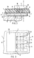
- Fig. 1 and Fig. 2 each show a cross section through a first embodiment of the cooling device according to the invention.
- a double copper-clad circuit board 1 made of insulating material has on its top 6 next to those for Wiring of components required a first conductor tracks large-area metallization 8 on and on the underside 7 a second large-area metallization 9, both over a plurality of through-metallized bores 10, so-called Vias, galvanically and thermally conductive with each other are connected.
- On the first large-scale metallization 8 is a heat generating electronic power device 2 over the plated-through holes 10 in a known manner Way e.g. soldered directly in the reflow soldering process.
- the solder application can take place so that solder 20 at least partially in the through-plated holes 10 of the top 6 is filled out.
- the thermal plate is in the form of a tin-plated Copper plate formed, the thickness of which is preferably approximately between 0.5 and 1.5 mm should be. But it is also conceivable another good heat-conducting material for the heat-conducting plate to use. Deviating from that in FIGS. 1 to Fig. 3 illustrated embodiment can the heat conducting plate 3, for example, the shape of a simple cuboid Have plate, the floor plan with the through-metallized Bore-provided area of the printed circuit board 1 corresponds. For soldering the heat conducting plate to the circuit board is then the circuit board 3, for example with the Bottom 7 turned upwards.
- FIG. 1 to 3 is the thermal plate 3, however, in the wave soldering process soldered to the second metallization 9. Because on the bottom 7 of the circuit board 1 often further components are provided are with the wave soldering method with connections the underside should be soldered, this has the advantage that the soldering of the thermal plate 3 together with the soldering these components can be done.
- FIG. 1 to Fig. 3 embodiment shows the thermal plate 3 a cuboid basic form, in the two rectangular recesses 15 are provided, which by three fingers 3a are delimited by one not with recesses project area 3b laterally. The recesses 15 are through the thermal plate from the top 18 passed through to the bottom 19. Like on can best be seen in FIG.
- the heat-conducting plate 3 an E-shaped floor plan.
- the one with the recesses the heat-conducting plate can also have a different shape.
- the area provided with the recesses is the Thermal plate at least the size of the via holes 10 provided area of the circuit board.
- the thermal plate 3 can be as follows on the circuit board 1 can be attached. First, on the top 18 of the not provided with the recesses, to the left in Fig. 3 the dashed line 3b arranged an adhesive 17 applied and then the thermal plate 3 with her Top 18 on the metallization 9 on the bottom 7 glued on the circuit board. It is important to ensure that area 3b is not on the plated through holes 10 is glued and that the recesses 15th provided, shown in Fig. 3 to the right of the dashed line Area above the plated-through holes 15 is arranged.
- the adhesive layer 17 serves to hold the Thermal plate during subsequent wave soldering and becomes very applied thinly.
- the heat-conducting plate is through the adhesive layer 17 through a very narrow gap from the second Metallization 9 spaced.
- the solder mask can also be applied prior to bonding be applied to the thermal plate.
- the one with the thermal plate provided circuit board is then one Wave soldering station supplied.
- wave soldering prevents Solder mask a solder deposit on the not with the recesses 15 provided area 3b of the underside 19 of the heat-conducting plate, while on the bottom 19 in the area the finger deposits 3a solder.
- solder 20 continues to penetrate into the recesses 15 and in the narrow gap between the second metallization 9 and the top 18 of the thermal plate.
- the through-plated holes 10 fill up Solder.
- At least the through the recesses are preferred 15 accessible holes 10 completely with solder replenished. This forms solder bridges, which the Vias 10 with the inner wall 14 of the recesses 15 very good heat conducting connection.
- the solder mask is removed and one in its place electrically insulating and good heat-conducting layer 5 the area 3b not provided with the plated-through holes applied to the underside 19 of the heat-conducting plate.
- the heat sink 4 has a raised area, which serves as a support area serves for the insulating layer 5. Below the The heat sink 4 has a depression, so that it is ensured that the deposited on the fingers 3a Lot 20 cannot touch the heat sink.
- the insulation layer 5 can also be designed as an adhesive layer or adhesive film be and thus the mechanical bracket serve the circuit board on the heat sink.
Landscapes
- Engineering & Computer Science (AREA)
- Microelectronics & Electronic Packaging (AREA)
- Chemical & Material Sciences (AREA)
- Materials Engineering (AREA)
- Physics & Mathematics (AREA)
- Condensed Matter Physics & Semiconductors (AREA)
- General Physics & Mathematics (AREA)
- Computer Hardware Design (AREA)
- Power Engineering (AREA)
- Cooling Or The Like Of Electrical Apparatus (AREA)
- Structure Of Printed Boards (AREA)
- Cooling Or The Like Of Semiconductors Or Solid State Devices (AREA)
Abstract
Description
Die Erfindung betrifft eine Kühlvorrichtung für ein auf einer Leiterplatte angeordnetes wärmeerzeugendes Bauelement mit den im Oberbegriff des Anspruchs 1 angegebenen Merkmalen.The invention relates to a cooling device for a Printed circuit board arranged heat-generating component with the Features specified in the preamble of claim 1.
Kühlvorrichtungen für auf Leiterplatten angeordnete elektronische Leistungsbauelemente haben seit einiger Zeit aufgrund der sehr starken Wärmeentwicklung moderner Leistungsbauelemente eine stets wachsende Bedeutung gewonnen. Eine möglichst effektive Wäremabfuhr ist dabei insbesondere in elektronischen Steuergeräten von Kraftfahrzeugen erforderlich, um Fehlfunktionen der Steuerelektronik zu vermeiden. Problematisch ist, daß die wärmeerzeugenden Bauelemente in den meisten Fällen gegenüber dem Kühlkörper elektrisch isoliert werden müssen, wobei die isolierende Schicht den direkten Wärmeübergang auf den Kühlkörper erschwert. So ist beispielsweise aus der DE 41 07 312 A1 eine Kühlvorrichtung mit einem auf eine doppelseitig kupferkaschierte Leiterplatte aufgelöteten wärmeerzeugenden Bauelement bekannt. Die von dem Bauelement erzeugte Wärme wird über durchmetallisierte Bohrungen in der Leiterplatte, sogenannte Durchkontaktierungen, die mit Lötzinn aufgefüllt sind und unmittelbar unter der Montagefläche des Bauelementes angeordnet sind, auf die kupferkaschierte Unterseite der Leiterplatte abgeleitet. Die Leiterplatte ist mit ihrer kupferkaschierten Unterseite getrennt durch eine wärmeleitende elektrisch isolierende Schicht auf einen Kühlkörper aufgebracht. Nachteilig dabei ist, daß die elektrisch isolierende Schicht einen schnellen Übergang der durch die metallisierten Bohrungen abgeleiteten Wärme auf den Kühlkörper verhindert, da die Wärmeleitfähigkeit dieser Schicht schlechter ist als die metallische Wärmeleitfähigkeit der mit Lot gefüllten durchmetallisierten Bohrungen. Bei sehr starker Wärmeentwicklung ist daher beim Stand der Technik ein nachteiliger Wärmestau die Folge, der zu einer Überhitzung und Beschädigung der auf der Leiterplatte angeordneten Schaltung führen kann.Cooling devices for electronic devices arranged on printed circuit boards Power components have been around for some time the very strong heat development of modern power components has become increasingly important. One if possible effective heat dissipation is particularly important in electronic Control devices of motor vehicles required to Avoid malfunctions in the control electronics. Problematic is that the heat generating components in most Cases are electrically isolated from the heat sink need, the insulating layer the direct heat transfer difficult on the heat sink. For example from DE 41 07 312 A1 a cooling device with a a double-sided copper-clad printed circuit board heat-generating component known. That of the component generated heat is through through-metallized holes in the Printed circuit board, so-called vias, with solder are filled and immediately below the mounting surface of the component are arranged on the copper-clad Derived from the bottom of the circuit board. The circuit board is with its copper-clad underside separated by a thermally conductive, electrically insulating layer on a heat sink upset. The disadvantage here is that the electrical insulating layer a quick transition through the Metallized holes dissipate heat to the heat sink prevents the thermal conductivity of this layer is worse than the metallic thermal conductivity of the Solder-filled through-metallized holes. With very strong Heat development is therefore a disadvantage in the prior art Heat build-up resulting in overheating and Damage to the circuit arranged on the circuit board can lead.
Die erfindungsgemäße Kühlvorrichtung mit den kennzeichnenden Merkmalen des Anspruchs 1 vermeidet die beim Stand der Technik auftretenden Nachteile. Ein Wärmestau der durch die metallisierten Bohrungen auf die der Montageseite des Bauelementes gegenüberliegende zweite Seite der Leiterplatte abgeleiteten Wärme wird vorteilhaft dadurch vermieden, daß eine als Wärmesenke dienende Wärmeleitplatte direkt auf die zweite großflächige Metallisierung unterhalb der durchmetallisierten Bohrungen aufgelötet ist. Dadurch wird vorteilhaft erreicht, daß die Wärme direkt auf die Wärmeleitplatte abgeleitet wird und sich dort rasch verteilt. Die Schichtdicken der großflächigen Metallisierungen der Leiterplatte beträgt bei einer doppelseitig kupferkaschierten Leiterplatte in der Regel 30 bis 40 µm und kann mit den bekannten Herstellungsverfahren kaum größer als 80µm ausgelegt werden, weshalb die laterale Wärmeableitung dieser Schicht nicht sehr groß ist. Im Gegensatz dazu kann die Wärmeleitplatte deutlich dicker als die Metallisierungsschicht ausgelegt werden, so daß die laterale Wärmeableitung deutlich verbessert wird. Besonders vorteilhaft ist, daß insbesondere bei einer kurzzeitig auftretenden Wärmepulsbelastung die Wärme zunächst direkt auf die Wärmeleitplatte abgeleitet wird, sich dort verteilt und anschließend über die elektrisch isolierende, wärmeleitende Schicht an den Kühlkörper abgegeben wird.The cooling device according to the invention with the characteristic Features of claim 1 avoids that in the prior art disadvantages. A build-up of heat due to the metallized Bores on the mounting side of the component opposite second side of the circuit board derived Heat is advantageously avoided in that a heat sink serving as a heat sink directly onto the second one large-area metallization below the through-metallized Holes is soldered. This advantageously achieves that the heat is dissipated directly to the heat conducting plate and spread out there quickly. The layer thicknesses of the large area Metallization of the circuit board is one double-sided copper-clad printed circuit board usually 30 up to 40 µm and can with the known manufacturing processes scarcely larger than 80µm, which is why the lateral Heat dissipation from this layer is not very large. In contrast in addition, the thermal plate can be significantly thicker than that Metallization layer are designed so that the lateral Heat dissipation is significantly improved. Particularly advantageous is that especially in the case of a briefly occurring Heat pulse load the heat directly onto the heat conducting plate is derived, distributed there and then over the electrically insulating, heat-conducting layer is delivered to the heat sink.
Vorteilhaft ist weiterhin als Wärmeleitplatte eine Metallplatte aus Kupfer zu verwenden, da dieses Material eine gute Lötfähigkeit und gleichzeitig eine hohe Wärmeleitfähigkeit besitzt.A metal plate is also advantageous as a heat-conducting plate made of copper, because this material is a good one Solderability and high thermal conductivity at the same time owns.
Besonders vorteilhaft ist weiterhin, den auf den durchmetallisierten Bohrungen aufliegenden Bereich der Wärmeleitplatte mit sich durch die Wärmeleitplatte erstreckenden Ausnehmungen zu versehen. Durch die Ausnehmungen ist ein Teil der durchmetallisierten Bohrungen von der zweiten Seite der Leiterplatte aus frei zugänglich, so daß nach Auflage der Wärmeleitplatte von der zweiten Seite der Leiterplatte aus Lötzinn durch die Ausnehmungen in die durchmetallisierten Löcher eingefüllt werden kann. Da das in die Ausnehmungen eingefüllte Lötzinn an den Innenwandungen der Ausnehmungen haftet und gleichzeitig in die metallisierten Bohrungen eindringt, bilden sich Lotbrücken aus, die die Wärmeableitung auf die Wärmeleitplatte deutlich verbessern. Eine derartige Verlötung der Wärmeleitplatte mit der zweiten Metallisierung der Leiterplatte kann vorteilhaft im gut beherrschten Wellenlötverfahren zusammen mit der Verlötung von auf der zweiten Seite der Leiterplatte vorgesehenen Bauelementen durchgeführt werden.It is also particularly advantageous that the on the metallized Bores on the area of the heat conducting plate with recesses extending through the heat-conducting plate to provide. Part of the through-metallized is through the recesses Holes from the second side of the circuit board from freely accessible, so that after laying the thermal plate from the second side of the PCB made of solder through the Recesses filled in the plated-through holes can be. Since the solder filled into the recesses adheres to the inner walls of the recesses and at the same time penetrates into the metallized holes, form Solder bridges that heat dissipation to the thermal plate improve significantly. Such a soldering of the heat conducting plate with the second metallization of the circuit board can be advantageous in well-controlled wave soldering together with the soldering from on the second side of the circuit board provided components are performed.
Weiterhin ist vorteilhaft, wenn die Ausnehmungen der Wärmeleitplatte derart angeordnet sind, daß der auf den durchmetallisierten Bohrungen aufliegende Bereich der Wärmeleitplatte eine kammartige Struktur mit mehrere parallelen Fingern aufweist. Durch eine Optimierung von Breite und Abstand der Finger kann eine gute Wärmeableitung erreicht werden und gleichzeitig sichergestellt werden, daß genügend durchmetallisierte Bohrungen beim Löten mit Lötzinn aufgefüllt werden.It is also advantageous if the recesses in the heat-conducting plate are arranged so that the on the metallized Area of the heat conducting plate lying on the bores a comb-like structure with several parallel fingers having. By optimizing the width and distance of the Good heat dissipation can be achieved and fingers at the same time ensure that there is enough metallization Holes are filled with solder when soldering.
Außerdem ist vorteilhaft, einen nicht mit Ausnehmungen versehenen weiteren Bereich der Wärmeableitplatte vorzusehen. Dieser Bereich kann auf einfache Weise vor dem Löten mit einem Lötstopplack oder einer Folie abgedeckt werden, welche eine Belotung verhindert, und dient bei der Montage der Leiterplatte auf dem Kühlkörper vorteilhaft als ebener Auflagebereich.It is also advantageous to use a recess that is not provided with recesses to provide further area of the heat dissipation plate. This The area can easily be soldered with a Solder mask or a film to be covered, which is a Soldering prevents and is used when assembling the circuit board on the heat sink advantageous as a flat support area.
Die Wärmeleitplatte kann besonders leicht mit der zweiten Metallisierung der Leiterplatte im Wellenlötverfahren verlötet werden. Hierzu wird der nicht mit den Ausnehmungen versehene Bereich zunächst über eine Klebeschicht auf die zweite Metallisierung aufgeklebt. Die Klebeschicht dient dann vorteilhaft als Positionierhilfe der Wärmeleitplatte beim anschließenden Wellenlöten.The thermal plate can be particularly easily with the second metallization the circuit board by wave soldering become. For this, the one not provided with the recesses First apply an adhesive layer to the second metallization glued. The adhesive layer then advantageously serves as a positioning aid for the thermal plate during the subsequent Wave soldering.
Ein Ausführungsbeispiel der Erfindung ist in der Zeichnung
dargestellt und wird in der nachfolgenden Beschreibung näher
erläutert. Es zeigt
Fig. 1 und Fig. 2 zeigen jeweils einen Querschnitt durch ein
erstes Ausführungsbeispiel der erfindungsgemäßen Kühlvorrichtung.
Eine doppelt kupferkaschierte Leiterplatte 1 aus Isoliermaterial
weist auf ihrer Oberseite 6 neben den für die
Verdrahtung von Bauelementen benötigten Leiterbahnen eine erste
großflächige Metallisierung 8 auf und auf der Unterseite
7 eine zweite großflächige Metallisierung 9, die beide über
eine Vielzahl von durchmetallisierten Bohrungen 10, sogenannte
Durchkontaktierungen, galvanisch und wärmeleitend miteinander
verbunden sind. Auf der ersten großflächigen Metallisierung
8 ist ein wärmeerzeugendes elektronisches Leistungsbauelement
2 über den durchmetallisierten Bohrungen 10 in bekannter
Weise z.B. im Reflow-Lötverfahren direkt aufgelötet.
Die Lotauftragung kann dabei so erfolgen, daß Lot 20 wenigstens
teilweise in die durchmetallisierten Bohrungen 10 von
der Oberseite 6 aus eingefüllt wird. Weiterhin sind Anschlüsse
13 des Bauelementes 2 mit Leiterbahnen 11 auf der Oberseite
der Leiterplatte 1 verlötet.Fig. 1 and Fig. 2 each show a cross section through a
first embodiment of the cooling device according to the invention.
A double copper-clad circuit board 1 made of insulating material
has on its
Auf der Unterseite 7 der Leiterplatte 1 ist eine Wärmeleitplatte
3 auf die zweite Metallisierung 9 direkt aufgelötet.
Die Wärmeleitplatte ist in Form einer galvanisch verzinnten
Kupferplatte ausgebildet, deren Dicke vorzugsweise etwa zwischen
0,5 und 1,5 mm liegen sollte. Es ist aber auch denkbar,
ein anderes gut wärmeleitendes Material für die Wärmeleitplatte
zu verwenden. Abweichend von dem in den Fig. 1 bis
Fig. 3 dargestellten Ausführungsbeispiel kann die Wärmeleitplatte
3 beispielsweise die Form einer einfachen quaderförmigen
Platte aufweisen, deren Grundriß dem mit den durchmetallisierten
Bohrungen versehenen Bereich der Leiterplatte 1
entspricht. Zur Verlötung der Wärmeleitplatte mit der Leiterplatte
wird dann die Leiterplatte 3 beispielsweise mit der
Unterseite 7 nach oben gewandt. Anschließend wird auf die
nunmehr oben liegende Seite 7 über den durchmetallisierten
Bohrungen Lot aufgedruckt, die Wärmeleitplatte 3 auf die Lotpaste
aufgesetzt und im Reflowlötverfahren mit der zweiten
Metallisierung 9 verlötet. Anschließend wird auf der von der
Leiterplatte abgewandten Seite der Wärmeleitplatte 3 die
elektrisch isolierende und wärmeleitende Schicht aufgebracht
und die Wärmeleitplatte mit der isolierende Schicht auf einen
Kühlkörper aufgesetzt.On the
Bei dem in den Figuren 1 bis 3 dargestellten Ausführungsbeispiel
ist die Wärmeleitplatte 3 jedoch im Wellenlötverfahren
mit der zweiten Metallisierung 9 verlötet. Da auf der Unterseite
7 der Leiterplatte 1 oft noch weitere Bauelemente vorgesehen
sind, die im Wellenlötverfahren mit Anschlüssen auf
der Unterseite verlötet werden sollen, hat dies den Vorteil,
daß die Verlötung der Wärmeleitplatte 3 zusammen mit der Verlötung
dieser Bauelemente erfolgen kann. Bei dem in Fig. 1
bis Fig. 3 dargestellten Ausführungsbeispiel weist die Wärmeleitplatte
3 eine quaderförmige Grundform auf, in der zwei
rechteckförmige Ausnehmungen 15 vorgesehen sind, die durch
drei Finger 3a begrenzt werden, die von einem nicht mit Ausnehmungen
versehenen Bereich 3b seitlich abstehen. Die Ausnehmungen
15 sind durch die Wärmeleitplatte von deren Oberseite
18 bis zu deren Unterseite 19 hindurchgeführt. Wie am
besten in Fig. 3 zu erkennen ist, weist die Wärmeleitplatte 3
einen E-förmigen Grundriß auf. Die mit den Ausnehmungen versehene
Wärmeleitplatte kann aber auch eine andere Form aufweisen.
Insbesondere ist es möglich, die Anzahl der Finger 3a
an die Anzahl der Durchkontaktierungen anzupassen. Vorteilhaft
ist, wenn der mit den Ausnehmungen versehene Bereich der
Wärmeleitplatte mindestens die Größe des mit den Durchkontaktierungen
10 versehenen Bereiches der Leiterplatte aufweist.In the embodiment shown in Figures 1 to 3
is the
Die Wärmeleitplatte 3 kann folgendermaßen an der Leiterplatte
1 befestigt werden. Zunächst wird auf die Oberseite 18 des
nicht mit den Ausnehmungen versehenen, in Fig. 3 links von
der gestrichelten Linie angeordneten Bereichs 3b ein Kleber
17 aufgetragen und anschließend die Wärmeleitplatte 3 mit ihrer
Oberseite 18 auf die Metallisierung 9 auf der Unterseite
7 der Leiterplatte aufgeklebt. Dabei ist darauf zu achten,
daß der Bereich 3b nicht auf die durchmetallisierten Bohrungen
10 aufgeklebt wird und daß der mit den Ausnehmungen 15
versehene, in Fig. 3 rechts von der gestrichelten Linie dargestellte
Bereich über den durchmetallisierten Bohrungen 15
angeordnet wird. Die Klebeschicht 17 dient der Halterung der
Wärmeleitplatte beim anschließenden Wellenlöten und wird sehr
dünn aufgetragen. Durch die Klebeschicht 17 ist die Wärmeleitplatte
durch einen sehr schmalen Spalt von der zweiten
Metallisierung 9 beabstandet. Weiterhin wird ein Lötstopplack
oder ein anderes geeignetes Mittel auf die Unterseite 19 des
nicht mit den Ausnehmungen versehenen Bereichs 3b aufgetragen.
Der Lötstopplack kann auch bereits vor der Verklebung
der Wärmeleitplatte aufgetragen werden. Die mit der Wärmeleitplatte
versehene Leiterplatte wird anschließend einer
Wellenlötstation zugeführt. Beim Wellenlöten verhindert der
Lötstopplack eine Lotabscheidung auf dem nicht mit den Ausnehmungen
15 versehenen Bereich 3b der Unterseite 19 der Wärmeleitplatte,
während sich auf der Unterseite 19 im Bereich
der Finger 3a Lot abscheidet. Wie besonders gut in Fig. 1 zu
erkennen ist, dringt Lötzinn 20 weiterhin auch in die Ausnehmungen
15 und in den schmalen Spalt zwischen der zweiten Metallisierung
9 und der Oberseite 18 der Wärmeleitplatte ein.
Außerdem füllen sich die durchmetallisierten Bohrungen 10 mit
Lötzinn. Vorzugsweise werden zumindest die durch die Ausnehmungen
15 zugänglichen Bohrungen 10 vollständig mit Lötzinn
aufgefüllt. Dabei bilden sich Lotbrücken aus, welche die
Durchkontaktierungen 10 mit der Innenwandung 14 der Ausnehmungen
15 sehr gut wärmeleitend verbinden. Nach der Verlötung
wird der Lötstopplack entfernt und an seiner Stelle eine
elektrisch isolierende und gut wärmeleitende Schicht 5 auf
den nicht mit den Durchkontaktierungen versehenen Bereich 3b
auf der Unterseite 19 der Wärmeleitplatte aufgebracht. Wird
ein Lötstopplack verwendet, der eine ausreichende Wärmeleitfähigkeit
und elektrisch isolierende Eigenschaften besitzt,
so kann dieser auch als Isolierschicht 5 vorgesehen sein, wodurch
ein Herstellungsschritt eingespart wird. Anschließend
wird die Leiterplatte 1 mit der Wärmeleitplatte 3, wie in
Fig. 2 gezeigt, auf einen Kühlkörper 4 aufgesetzt. Der Kühlkörper
4 weist einen erhabenen Bereich auf, welcher als Auflagebereich
für die Isolierschicht 5 dient. Unterhalb der
Fingerbereiche 3a weist der Kühlkörper 4 eine Absenkung auf,
so daß sicher gestellt ist, daß das auf den Fingern 3a abgeschiedene
Lot 20 nicht den Kühlkörper berühren kann. Die Isolierschicht
5 kann auch als Klebeschicht oder Klebefolie ausgebildet
sein und damit zugleich der mechanischen Halterung
der Leiterplatte auf dem Kühlkörper dienen.The
Durch die in Fig. 1 und 2 dargestellt Anordnung wird eine
sehr effektive Einkopplung der durch die Durchkontaktierungen
10 abgeleiteten Wärme auf die Fingerbereiche 3a der Wärmeleitplatte
3 erreicht. Die die Ausnehmungen 15 begrenzenden
Finger 3a leiten die Wärme auf den Bereich 3b ab. Dort verteilt
sich die Wärme und gelangt über die elektrisch isolierende
Schicht 5 auf den Kühlkörper 4. Je breiter die Fingerbereiche
3a ausgebildet sind, desto besser ist die laterale
Wärmeableitung auf den Bereich 3b. Andererseits sollten die
Finger nicht zu breit sein, da ansonsten zu viele Durchkontaktierungen
10 nicht mit Lot gefüllt werden. Fur die jeweilige
Anwendung muß hier ein Kompromiß gefunden werden. Bei
dem hier dargestellten Ausführungsbeispiel wurden die Breite
der Finger 3a etwa schmaler als die Breite der Ausnehmungen
15 ausgelegt.Due to the arrangement shown in FIGS. 1 and 2, a
very effective coupling of through-
Anders als in den Fig. 1 und 2 dargestellten Ausführungsbeispiel
ist es auch möglich, die Klebeschicht 17 entfallen zulassen
und statt dessen die Wärmeleitplatte 3 mit einer auf
der Unterseite 9 über dem Bereich 3b aufgeklebten Klebefolie
an der Unterseite 7 der Leiterplatte 1 festzukleben. Die Klebefolie
schützt in diesem Fall zugleich die Unterseite 19 des
Bereichs 3b vor einer Belotung in der Wellenlötstation. Beim
Löten dringt Lot 20 in die Ausnehmungen 15 und die Durchkontierungen
10 ein, wodurch die Wärmeleitplatte mit der zweiten
Metallisierung 9 verlötet wird. In diesem Fall liegt die
Oberseite 18 der Wärmeleitplatte direkt auf der zweiten Metallisierung
9 auf.Unlike the embodiment shown in FIGS. 1 and 2
it is also possible to omit the
Claims (8)
Applications Claiming Priority (2)
| Application Number | Priority Date | Filing Date | Title |
|---|---|---|---|
| DE1997152797 DE19752797A1 (en) | 1997-11-28 | 1997-11-28 | Cooling device for a heat-generating component arranged on a printed circuit board |
| DE19752797 | 1997-11-28 |
Publications (3)
| Publication Number | Publication Date |
|---|---|
| EP0920055A2 true EP0920055A2 (en) | 1999-06-02 |
| EP0920055A3 EP0920055A3 (en) | 1999-07-28 |
| EP0920055B1 EP0920055B1 (en) | 2005-11-30 |
Family
ID=7850109
Family Applications (1)
| Application Number | Title | Priority Date | Filing Date |
|---|---|---|---|
| EP19980115694 Expired - Lifetime EP0920055B1 (en) | 1997-11-28 | 1998-08-20 | Cooling device for a heat generating component on a printed board |
Country Status (3)
| Country | Link |
|---|---|
| EP (1) | EP0920055B1 (en) |
| JP (1) | JP4469429B2 (en) |
| DE (2) | DE19752797A1 (en) |
Cited By (18)
| Publication number | Priority date | Publication date | Assignee | Title |
|---|---|---|---|---|
| WO2001006821A1 (en) * | 1999-07-15 | 2001-01-25 | Incep Technologies, Inc. | Encapsulated packaging in between 2 pcbs |
| US6356448B1 (en) | 1999-11-02 | 2002-03-12 | Inceptechnologies, Inc. | Inter-circuit encapsulated packaging for power delivery |
| FR2819372A1 (en) * | 2001-01-09 | 2002-07-12 | Deere & Co | PRINTED CIRCUIT BOARD WITH HEAT EVALUATION |
| US6452113B2 (en) | 1999-07-15 | 2002-09-17 | Incep Technologies, Inc. | Apparatus for providing power to a microprocessor with integrated thermal and EMI management |
| WO2003019997A1 (en) * | 2001-08-22 | 2003-03-06 | Vanner, Inc. | Improved heat sink for surface mounted power devices |
| US6618268B2 (en) | 1999-07-15 | 2003-09-09 | Incep Technologies, Inc. | Apparatus for delivering power to high performance electronic assemblies |
| US6623279B2 (en) | 1999-07-15 | 2003-09-23 | Incep Technologies, Inc. | Separable power delivery connector |
| US6741480B2 (en) | 1999-07-15 | 2004-05-25 | Incep Technologies, Inc. | Integrated power delivery with flex circuit interconnection for high density power circuits for integrated circuits and systems |
| US6801431B2 (en) | 1999-07-15 | 2004-10-05 | Incep Technologies, Inc. | Integrated power delivery and cooling system for high power microprocessors |
| EP1603376A1 (en) * | 2004-06-03 | 2005-12-07 | BREE (Beauce Réalisations et Études Électroniques) | Printed circuit by selective deposition |
| EP1903839A2 (en) | 2006-09-20 | 2008-03-26 | Sumitomo Wiring Systems, Ltd. | A method for producing a printed circuit board with a heat radiating structure and a printed circuit board with a heat radiating structure |
| WO2010012271A2 (en) * | 2008-07-30 | 2010-02-04 | Brose Fahrzeugteile Gmbh & Co. Kg, Würzburg | Apparatus, in particular for conducting current, and a method for producing an apparatus, in particular for conducting current |
| US7881072B2 (en) | 1999-07-15 | 2011-02-01 | Molex Incorporated | System and method for processor power delivery and thermal management |
| EP2388812A2 (en) * | 2010-05-17 | 2011-11-23 | Sunonwealth Electric Machine Industry Co., Ltd. | Heat dissipating assembly |
| US8794797B2 (en) | 2003-11-07 | 2014-08-05 | Teknoware Oy | Hybrid illuminator |
| ITMI20130520A1 (en) * | 2013-04-05 | 2014-10-06 | St Microelectronics Srl | CONSTRUCTION OF A HEAT SINK THROUGH WELDING |
| EP3203513A1 (en) * | 2016-02-05 | 2017-08-09 | Robert Bosch GmbH | Contact system with a circuit carrier and component |
| WO2018158061A1 (en) * | 2017-03-02 | 2018-09-07 | HELLA GmbH & Co. KGaA | Method for producing an electrical assembly |
Families Citing this family (21)
| Publication number | Priority date | Publication date | Assignee | Title |
|---|---|---|---|---|
| DE10033352B4 (en) * | 2000-07-08 | 2010-08-19 | Robert Bosch Gmbh | Method for producing an electronic assembly and electronic assembly |
| KR20020074073A (en) * | 2001-03-16 | 2002-09-28 | 엘지전자 주식회사 | Heat dissipation structure of ic |
| JP2003289191A (en) | 2002-03-28 | 2003-10-10 | Denso Corp | Electronic control device |
| DE10343429B4 (en) * | 2002-10-14 | 2007-08-16 | Heidelberger Druckmaschinen Ag | Arrangement for cooling an arranged on a printed circuit board electrical component |
| DE10335805A1 (en) * | 2003-08-05 | 2005-03-17 | Schweizer Electronic Ag | Circuit board with metal base forming potential reference plane and heat sink for power-dissipating components, includes both electrical and thermal vias for heat dissipation |
| JP4461268B2 (en) * | 2004-03-30 | 2010-05-12 | Dowaメタルテック株式会社 | Semiconductor device component, manufacturing method thereof, and semiconductor device using the same |
| JP2007036172A (en) * | 2005-11-28 | 2007-02-08 | Shin Kobe Electric Mach Co Ltd | Multilayer circuit board |
| DE102006004320A1 (en) * | 2006-01-31 | 2007-08-09 | Häusermann GmbH | Printed circuit board with functional elements and selectively filled and thermally conductive through-holes as well as manufacturing process and application |
| JP4992532B2 (en) * | 2006-04-27 | 2012-08-08 | パナソニック株式会社 | Heat dissipation board and manufacturing method thereof |
| US7410297B2 (en) | 2006-08-18 | 2008-08-12 | General Electric Company | Apparatus for controlling radiation in a radiation generator |
| DE102007039800B3 (en) * | 2007-08-23 | 2008-12-11 | Festo Ag & Co. Kg | Cooling device for electronic component, has interconnected device with end-sided connection section and carrying section of electronic component, and two sections are connected together by narrow bridge-shaped section |
| DE102007044358A1 (en) | 2007-09-17 | 2009-03-19 | Robert Bosch Gmbh | Device for cooling electronic components |
| DE102007057533B4 (en) * | 2007-11-29 | 2016-07-07 | Fraunhofer-Gesellschaft zur Förderung der angewandten Forschung e.V. | Heat sink, method for manufacturing a heat sink and printed circuit board with heat sink |
| DE102008019797B4 (en) * | 2008-04-18 | 2023-09-21 | Sew-Eurodrive Gmbh & Co Kg | Cooling arrangement and inverter |
| US10912186B2 (en) | 2015-12-03 | 2021-02-02 | Mitsubishi Electric Corporation | Semiconductor device |
| DE102016220833A1 (en) | 2016-10-24 | 2018-04-26 | Robert Bosch Gmbh | Control unit with an electronic component connected in a heat-conducting manner to the housing |
| US20200098660A1 (en) | 2017-05-26 | 2020-03-26 | Mitsubishi Electric Corporation | Semiconductor device |
| CN107191795A (en) * | 2017-06-06 | 2017-09-22 | 安徽艳阳电气集团有限公司 | A kind of LED lamp based on high heat dispersion |
| WO2019117107A1 (en) | 2017-12-14 | 2019-06-20 | 三菱電機株式会社 | Semiconductor device |
| DE102018109920A1 (en) * | 2018-04-25 | 2019-10-31 | Dr. Ing. H.C. F. Porsche Aktiengesellschaft | Cooling of power electronic circuits |
| US20200006021A1 (en) * | 2018-06-28 | 2020-01-02 | Black & Decker Inc. | Electronic switch module with oppositely-arranged power switches and discrete heat sinks |
Citations (6)
| Publication number | Priority date | Publication date | Assignee | Title |
|---|---|---|---|---|
| US5014904A (en) * | 1990-01-16 | 1991-05-14 | Cray Research, Inc. | Board-mounted thermal path connector and cold plate |
| DE4107312A1 (en) * | 1991-03-07 | 1992-09-10 | Telefunken Electronic Gmbh | Mounting system for power semiconductor device - has heat conductive coupling between heat conductive layer beneath semiconductor device and insulating layer supporting circuit board |
| EP0590354A1 (en) * | 1992-09-29 | 1994-04-06 | Robert Bosch Gmbh | Device with a board, a heat sink and at least one power component |
| FR2706730A1 (en) * | 1993-06-18 | 1994-12-23 | Sagem | Power electronics module having a heat-sink support |
| EP0634890A1 (en) * | 1993-07-12 | 1995-01-18 | Nec Corporation | Packaging structure for microwave circuit |
| DE19506664A1 (en) * | 1995-02-25 | 1996-02-29 | Bosch Gmbh Robert | Electric control apparatus for vehicle IC engine electromechanical mechanism |
-
1997
- 1997-11-28 DE DE1997152797 patent/DE19752797A1/en not_active Ceased
-
1998
- 1998-08-20 EP EP19980115694 patent/EP0920055B1/en not_active Expired - Lifetime
- 1998-08-20 DE DE59813241T patent/DE59813241D1/en not_active Expired - Lifetime
- 1998-11-27 JP JP33755198A patent/JP4469429B2/en not_active Expired - Lifetime
Patent Citations (6)
| Publication number | Priority date | Publication date | Assignee | Title |
|---|---|---|---|---|
| US5014904A (en) * | 1990-01-16 | 1991-05-14 | Cray Research, Inc. | Board-mounted thermal path connector and cold plate |
| DE4107312A1 (en) * | 1991-03-07 | 1992-09-10 | Telefunken Electronic Gmbh | Mounting system for power semiconductor device - has heat conductive coupling between heat conductive layer beneath semiconductor device and insulating layer supporting circuit board |
| EP0590354A1 (en) * | 1992-09-29 | 1994-04-06 | Robert Bosch Gmbh | Device with a board, a heat sink and at least one power component |
| FR2706730A1 (en) * | 1993-06-18 | 1994-12-23 | Sagem | Power electronics module having a heat-sink support |
| EP0634890A1 (en) * | 1993-07-12 | 1995-01-18 | Nec Corporation | Packaging structure for microwave circuit |
| DE19506664A1 (en) * | 1995-02-25 | 1996-02-29 | Bosch Gmbh Robert | Electric control apparatus for vehicle IC engine electromechanical mechanism |
Non-Patent Citations (1)
| Title |
|---|
| "INTERFACE MATERIALS OFFER HEAT TRANSFER AND ISOLATION" ELECTRONIC PACKAGING AND PRODUCTION, Bd. 35, Nr. 10, 1. September 1995, Seite 32 XP000532275 * |
Cited By (28)
| Publication number | Priority date | Publication date | Assignee | Title |
|---|---|---|---|---|
| US6741480B2 (en) | 1999-07-15 | 2004-05-25 | Incep Technologies, Inc. | Integrated power delivery with flex circuit interconnection for high density power circuits for integrated circuits and systems |
| US6304450B1 (en) | 1999-07-15 | 2001-10-16 | Incep Technologies, Inc. | Inter-circuit encapsulated packaging |
| US7245507B2 (en) | 1999-07-15 | 2007-07-17 | Dibene Ii Joseph T | Method and apparatus for providing power to a microprocessor with integrated thermal and EMI management |
| US6452113B2 (en) | 1999-07-15 | 2002-09-17 | Incep Technologies, Inc. | Apparatus for providing power to a microprocessor with integrated thermal and EMI management |
| WO2001006821A1 (en) * | 1999-07-15 | 2001-01-25 | Incep Technologies, Inc. | Encapsulated packaging in between 2 pcbs |
| US6801431B2 (en) | 1999-07-15 | 2004-10-05 | Incep Technologies, Inc. | Integrated power delivery and cooling system for high power microprocessors |
| US6618268B2 (en) | 1999-07-15 | 2003-09-09 | Incep Technologies, Inc. | Apparatus for delivering power to high performance electronic assemblies |
| US6623279B2 (en) | 1999-07-15 | 2003-09-23 | Incep Technologies, Inc. | Separable power delivery connector |
| US7881072B2 (en) | 1999-07-15 | 2011-02-01 | Molex Incorporated | System and method for processor power delivery and thermal management |
| US6356448B1 (en) | 1999-11-02 | 2002-03-12 | Inceptechnologies, Inc. | Inter-circuit encapsulated packaging for power delivery |
| GB2375655B (en) * | 2001-01-09 | 2004-03-10 | Deere & Co | Circuit board assembly |
| GB2375655A (en) * | 2001-01-09 | 2002-11-20 | Deere & Co | Circuit board assembly |
| FR2819372A1 (en) * | 2001-01-09 | 2002-07-12 | Deere & Co | PRINTED CIRCUIT BOARD WITH HEAT EVALUATION |
| WO2003019997A1 (en) * | 2001-08-22 | 2003-03-06 | Vanner, Inc. | Improved heat sink for surface mounted power devices |
| US8794797B2 (en) | 2003-11-07 | 2014-08-05 | Teknoware Oy | Hybrid illuminator |
| EP1603376A1 (en) * | 2004-06-03 | 2005-12-07 | BREE (Beauce Réalisations et Études Électroniques) | Printed circuit by selective deposition |
| EP1903839A2 (en) | 2006-09-20 | 2008-03-26 | Sumitomo Wiring Systems, Ltd. | A method for producing a printed circuit board with a heat radiating structure and a printed circuit board with a heat radiating structure |
| US7606038B2 (en) | 2006-09-20 | 2009-10-20 | Sumitomo Wiring Systems, Ltd. | Method for producing a printed circuit board with a heat radiating structure and a printed circuit board with a heat radiating structure |
| EP1903839A3 (en) * | 2006-09-20 | 2009-05-27 | Sumitomo Wiring Systems, Ltd. | A method for producing a printed circuit board with a heat radiating structure and a printed circuit board with a heat radiating structure |
| WO2010012271A3 (en) * | 2008-07-30 | 2010-05-06 | Brose Fahrzeugteile Gmbh & Co. Kg, Würzburg | Apparatus, in particular for conducting current, and a method for producing an apparatus, in particular for conducting current |
| WO2010012271A2 (en) * | 2008-07-30 | 2010-02-04 | Brose Fahrzeugteile Gmbh & Co. Kg, Würzburg | Apparatus, in particular for conducting current, and a method for producing an apparatus, in particular for conducting current |
| EP2388812A2 (en) * | 2010-05-17 | 2011-11-23 | Sunonwealth Electric Machine Industry Co., Ltd. | Heat dissipating assembly |
| ITMI20130520A1 (en) * | 2013-04-05 | 2014-10-06 | St Microelectronics Srl | CONSTRUCTION OF A HEAT SINK THROUGH WELDING |
| US9237644B2 (en) | 2013-04-05 | 2016-01-12 | Stmicroelectronics S.R.L. | Manufacturing of a heat sink by wave soldering |
| US9615444B2 (en) | 2013-04-05 | 2017-04-04 | Stmicroelectronics S.R.L. | Manufacturing of a heat sink by wave soldering |
| EP3203513A1 (en) * | 2016-02-05 | 2017-08-09 | Robert Bosch GmbH | Contact system with a circuit carrier and component |
| WO2018158061A1 (en) * | 2017-03-02 | 2018-09-07 | HELLA GmbH & Co. KGaA | Method for producing an electrical assembly |
| CN110352632A (en) * | 2017-03-02 | 2019-10-18 | 黑拉有限责任两合公司 | Method for manufacturing electric component |
Also Published As
| Publication number | Publication date |
|---|---|
| JP4469429B2 (en) | 2010-05-26 |
| JPH11345921A (en) | 1999-12-14 |
| DE19752797A1 (en) | 1999-06-10 |
| DE59813241D1 (en) | 2006-01-05 |
| EP0920055B1 (en) | 2005-11-30 |
| EP0920055A3 (en) | 1999-07-28 |
Similar Documents
| Publication | Publication Date | Title |
|---|---|---|
| EP0920055B1 (en) | Cooling device for a heat generating component on a printed board | |
| EP0934687B1 (en) | Assembly consisting of a substrate for power components and a cooling element and method for the production thereof | |
| DE102011083223B4 (en) | Power semiconductor module with integrated thick-film circuit board | |
| EP2043412B1 (en) | Conductor rail with heat conduction | |
| DE112016005794B4 (en) | Circuit arrangement and electrical junction box | |
| DE19634202C2 (en) | Semiconductor device | |
| EP1929847B1 (en) | Printed board | |
| DE19928788A1 (en) | Ceramic electronic component such as a laminated ceramic capacitor | |
| DE102004021054B4 (en) | Semiconductor component and method for its production | |
| DE4326506A1 (en) | Electrical appliance, in particular a switching device or controller for motor vehicles | |
| DE102013100701B4 (en) | SEMICONDUCTOR MODULE ARRANGEMENT AND METHOD FOR MANUFACTURING A SEMICONDUCTOR MODULE ARRANGEMENT | |
| EP1445799B1 (en) | Heat dissipation device for a semiconductor on a printed circuit board | |
| DE4335946C2 (en) | Arrangement consisting of a printed circuit board | |
| EP3095307B1 (en) | Printed circuit board, circuit, and method for the production of a circuit | |
| DE19509441A1 (en) | Hybrid integrated circuit | |
| EP0881866A1 (en) | Control device | |
| DE202014006215U1 (en) | Printed circuit board with cooled component, in particular SMD component | |
| EP0938252A2 (en) | Electrical circuit arrangement | |
| EP0849981B1 (en) | Doublesided or multilayered copper laminated printed circuit board and method of making the same | |
| DE10127773A1 (en) | Capacitor module for inverter has switching module attached to lower substrate of stack on which ceramic capacitors are mounted | |
| DE10064221B4 (en) | Printed circuit board with cooled SMD component | |
| DE19805492C2 (en) | Circuit board | |
| DE10217214B4 (en) | Cooling arrangement for a circuit arrangement | |
| DE102019113021A1 (en) | Electronic component for a vehicle with improved electrical contacting of a semiconductor component and manufacturing method | |
| EP0651598B1 (en) | Electronic circuit module |
Legal Events
| Date | Code | Title | Description |
|---|---|---|---|
| PUAI | Public reference made under article 153(3) epc to a published international application that has entered the european phase |
Free format text: ORIGINAL CODE: 0009012 |
|
| AK | Designated contracting states |
Kind code of ref document: A2 Designated state(s): DE FR GB IT |
|
| AX | Request for extension of the european patent |
Free format text: AL;LT;LV;MK;RO;SI |
|
| PUAL | Search report despatched |
Free format text: ORIGINAL CODE: 0009013 |
|
| AK | Designated contracting states |
Kind code of ref document: A3 Designated state(s): AT BE CH CY DE DK ES FI FR GB GR IE IT LI LU MC NL PT SE |
|
| AX | Request for extension of the european patent |
Free format text: AL;LT;LV;MK;RO;SI |
|
| RIC1 | Information provided on ipc code assigned before grant |
Free format text: 6H 05K 1/02 A, 6H 05K 7/20 B |
|
| 17P | Request for examination filed |
Effective date: 20000128 |
|
| AKX | Designation fees paid |
Free format text: DE FR GB IT |
|
| 17Q | First examination report despatched |
Effective date: 20041012 |
|
| GRAP | Despatch of communication of intention to grant a patent |
Free format text: ORIGINAL CODE: EPIDOSNIGR1 |
|
| RTI1 | Title (correction) |
Free format text: COOLING DEVICE FOR A HEAT GENERATING COMPONENT ON A PRINTED BOARD |
|
| GRAS | Grant fee paid |
Free format text: ORIGINAL CODE: EPIDOSNIGR3 |
|
| GRAA | (expected) grant |
Free format text: ORIGINAL CODE: 0009210 |
|
| AK | Designated contracting states |
Kind code of ref document: B1 Designated state(s): DE FR GB IT |
|
| PG25 | Lapsed in a contracting state [announced via postgrant information from national office to epo] |
Ref country code: GB Free format text: LAPSE BECAUSE OF FAILURE TO SUBMIT A TRANSLATION OF THE DESCRIPTION OR TO PAY THE FEE WITHIN THE PRESCRIBED TIME-LIMIT Effective date: 20051130 |
|
| REG | Reference to a national code |
Ref country code: GB Ref legal event code: FG4D Free format text: NOT ENGLISH |
|
| REF | Corresponds to: |
Ref document number: 59813241 Country of ref document: DE Date of ref document: 20060105 Kind code of ref document: P |
|
| GBV | Gb: ep patent (uk) treated as always having been void in accordance with gb section 77(7)/1977 [no translation filed] |
Effective date: 20051130 |
|
| ET | Fr: translation filed | ||
| PLBE | No opposition filed within time limit |
Free format text: ORIGINAL CODE: 0009261 |
|
| STAA | Information on the status of an ep patent application or granted ep patent |
Free format text: STATUS: NO OPPOSITION FILED WITHIN TIME LIMIT |
|
| 26N | No opposition filed |
Effective date: 20060831 |
|
| PGFP | Annual fee paid to national office [announced via postgrant information from national office to epo] |
Ref country code: FR Payment date: 20090819 Year of fee payment: 12 |
|
| PGFP | Annual fee paid to national office [announced via postgrant information from national office to epo] |
Ref country code: DE Payment date: 20091026 Year of fee payment: 12 |
|
| PGFP | Annual fee paid to national office [announced via postgrant information from national office to epo] |
Ref country code: IT Payment date: 20090824 Year of fee payment: 12 |
|
| REG | Reference to a national code |
Ref country code: FR Ref legal event code: ST Effective date: 20110502 |
|
| PG25 | Lapsed in a contracting state [announced via postgrant information from national office to epo] |
Ref country code: IT Free format text: LAPSE BECAUSE OF NON-PAYMENT OF DUE FEES Effective date: 20100820 |
|
| REG | Reference to a national code |
Ref country code: DE Ref legal event code: R119 Ref document number: 59813241 Country of ref document: DE Effective date: 20110301 |
|
| PG25 | Lapsed in a contracting state [announced via postgrant information from national office to epo] |
Ref country code: DE Free format text: LAPSE BECAUSE OF NON-PAYMENT OF DUE FEES Effective date: 20110301 Ref country code: FR Free format text: LAPSE BECAUSE OF NON-PAYMENT OF DUE FEES Effective date: 20100831 |