EP0922305B1 - Uv/blue led-phosphor device with efficient conversion of uv/blue light to visible light - Google Patents
Uv/blue led-phosphor device with efficient conversion of uv/blue light to visible light Download PDFInfo
- Publication number
- EP0922305B1 EP0922305B1 EP98917519A EP98917519A EP0922305B1 EP 0922305 B1 EP0922305 B1 EP 0922305B1 EP 98917519 A EP98917519 A EP 98917519A EP 98917519 A EP98917519 A EP 98917519A EP 0922305 B1 EP0922305 B1 EP 0922305B1
- Authority
- EP
- European Patent Office
- Prior art keywords
- visible light
- led
- light emitting
- blue
- filter
- Prior art date
- Legal status (The legal status is an assumption and is not a legal conclusion. Google has not performed a legal analysis and makes no representation as to the accuracy of the status listed.)
- Expired - Lifetime
Links
Images


Classifications
-
- H—ELECTRICITY
- H01—ELECTRIC ELEMENTS
- H01L—SEMICONDUCTOR DEVICES NOT COVERED BY CLASS H10
- H01L33/00—Semiconductor devices with at least one potential-jump barrier or surface barrier specially adapted for light emission; Processes or apparatus specially adapted for the manufacture or treatment thereof or of parts thereof; Details thereof
- H01L33/48—Semiconductor devices with at least one potential-jump barrier or surface barrier specially adapted for light emission; Processes or apparatus specially adapted for the manufacture or treatment thereof or of parts thereof; Details thereof characterised by the semiconductor body packages
- H01L33/50—Wavelength conversion elements
- H01L33/501—Wavelength conversion elements characterised by the materials, e.g. binder
- H01L33/502—Wavelength conversion materials
-
- H—ELECTRICITY
- H04—ELECTRIC COMMUNICATION TECHNIQUE
- H04N—PICTORIAL COMMUNICATION, e.g. TELEVISION
- H04N9/00—Details of colour television systems
- H04N9/12—Picture reproducers
- H04N9/30—Picture reproducers using solid-state colour display devices
-
- H—ELECTRICITY
- H01—ELECTRIC ELEMENTS
- H01L—SEMICONDUCTOR DEVICES NOT COVERED BY CLASS H10
- H01L2224/00—Indexing scheme for arrangements for connecting or disconnecting semiconductor or solid-state bodies and methods related thereto as covered by H01L24/00
- H01L2224/01—Means for bonding being attached to, or being formed on, the surface to be connected, e.g. chip-to-package, die-attach, "first-level" interconnects; Manufacturing methods related thereto
- H01L2224/26—Layer connectors, e.g. plate connectors, solder or adhesive layers; Manufacturing methods related thereto
- H01L2224/31—Structure, shape, material or disposition of the layer connectors after the connecting process
- H01L2224/32—Structure, shape, material or disposition of the layer connectors after the connecting process of an individual layer connector
- H01L2224/321—Disposition
- H01L2224/32151—Disposition the layer connector connecting between a semiconductor or solid-state body and an item not being a semiconductor or solid-state body, e.g. chip-to-substrate, chip-to-passive
- H01L2224/32221—Disposition the layer connector connecting between a semiconductor or solid-state body and an item not being a semiconductor or solid-state body, e.g. chip-to-substrate, chip-to-passive the body and the item being stacked
- H01L2224/32245—Disposition the layer connector connecting between a semiconductor or solid-state body and an item not being a semiconductor or solid-state body, e.g. chip-to-substrate, chip-to-passive the body and the item being stacked the item being metallic
- H01L2224/32257—Disposition the layer connector connecting between a semiconductor or solid-state body and an item not being a semiconductor or solid-state body, e.g. chip-to-substrate, chip-to-passive the body and the item being stacked the item being metallic the layer connector connecting to a bonding area disposed in a recess of the surface of the item
-
- H—ELECTRICITY
- H01—ELECTRIC ELEMENTS
- H01L—SEMICONDUCTOR DEVICES NOT COVERED BY CLASS H10
- H01L2224/00—Indexing scheme for arrangements for connecting or disconnecting semiconductor or solid-state bodies and methods related thereto as covered by H01L24/00
- H01L2224/01—Means for bonding being attached to, or being formed on, the surface to be connected, e.g. chip-to-package, die-attach, "first-level" interconnects; Manufacturing methods related thereto
- H01L2224/42—Wire connectors; Manufacturing methods related thereto
- H01L2224/47—Structure, shape, material or disposition of the wire connectors after the connecting process
- H01L2224/48—Structure, shape, material or disposition of the wire connectors after the connecting process of an individual wire connector
- H01L2224/4805—Shape
- H01L2224/4809—Loop shape
- H01L2224/48091—Arched
-
- H—ELECTRICITY
- H01—ELECTRIC ELEMENTS
- H01L—SEMICONDUCTOR DEVICES NOT COVERED BY CLASS H10
- H01L2224/00—Indexing scheme for arrangements for connecting or disconnecting semiconductor or solid-state bodies and methods related thereto as covered by H01L24/00
- H01L2224/01—Means for bonding being attached to, or being formed on, the surface to be connected, e.g. chip-to-package, die-attach, "first-level" interconnects; Manufacturing methods related thereto
- H01L2224/42—Wire connectors; Manufacturing methods related thereto
- H01L2224/47—Structure, shape, material or disposition of the wire connectors after the connecting process
- H01L2224/48—Structure, shape, material or disposition of the wire connectors after the connecting process of an individual wire connector
- H01L2224/481—Disposition
- H01L2224/48151—Connecting between a semiconductor or solid-state body and an item not being a semiconductor or solid-state body, e.g. chip-to-substrate, chip-to-passive
- H01L2224/48221—Connecting between a semiconductor or solid-state body and an item not being a semiconductor or solid-state body, e.g. chip-to-substrate, chip-to-passive the body and the item being stacked
- H01L2224/48245—Connecting between a semiconductor or solid-state body and an item not being a semiconductor or solid-state body, e.g. chip-to-substrate, chip-to-passive the body and the item being stacked the item being metallic
- H01L2224/48247—Connecting between a semiconductor or solid-state body and an item not being a semiconductor or solid-state body, e.g. chip-to-substrate, chip-to-passive the body and the item being stacked the item being metallic connecting the wire to a bond pad of the item
-
- H—ELECTRICITY
- H01—ELECTRIC ELEMENTS
- H01L—SEMICONDUCTOR DEVICES NOT COVERED BY CLASS H10
- H01L2224/00—Indexing scheme for arrangements for connecting or disconnecting semiconductor or solid-state bodies and methods related thereto as covered by H01L24/00
- H01L2224/73—Means for bonding being of different types provided for in two or more of groups H01L2224/10, H01L2224/18, H01L2224/26, H01L2224/34, H01L2224/42, H01L2224/50, H01L2224/63, H01L2224/71
- H01L2224/732—Location after the connecting process
- H01L2224/73251—Location after the connecting process on different surfaces
- H01L2224/73265—Layer and wire connectors
-
- H—ELECTRICITY
- H01—ELECTRIC ELEMENTS
- H01L—SEMICONDUCTOR DEVICES NOT COVERED BY CLASS H10
- H01L33/00—Semiconductor devices with at least one potential-jump barrier or surface barrier specially adapted for light emission; Processes or apparatus specially adapted for the manufacture or treatment thereof or of parts thereof; Details thereof
- H01L33/44—Semiconductor devices with at least one potential-jump barrier or surface barrier specially adapted for light emission; Processes or apparatus specially adapted for the manufacture or treatment thereof or of parts thereof; Details thereof characterised by the coatings, e.g. passivation layer or anti-reflective coating
-
- Y—GENERAL TAGGING OF NEW TECHNOLOGICAL DEVELOPMENTS; GENERAL TAGGING OF CROSS-SECTIONAL TECHNOLOGIES SPANNING OVER SEVERAL SECTIONS OF THE IPC; TECHNICAL SUBJECTS COVERED BY FORMER USPC CROSS-REFERENCE ART COLLECTIONS [XRACs] AND DIGESTS
- Y10—TECHNICAL SUBJECTS COVERED BY FORMER USPC
- Y10S—TECHNICAL SUBJECTS COVERED BY FORMER USPC CROSS-REFERENCE ART COLLECTIONS [XRACs] AND DIGESTS
- Y10S362/00—Illumination
- Y10S362/80—Light emitting diode
Definitions
- This invention relates to light emitting devices comprising a UV/blue-emitting light emitting diode (LED) and a UV/blue-excitable, visible light emitting phosphor.
- LED light emitting diode
- Such light emitting devices are disclosed in Japanese Kokai No. 5-152609 , and in WO 97/48138 , filed in the name of Applicant.
- UV/blue LED means an LED emitting in the UV range, or in the blue range, or in both the UV and blue ranges of the electromagnetic spectrum.
- LED's Visible light emitting diodes
- These are multilayer epitaxial structures based mainly on AlGaAs and InGaAlP as basic materials.
- the light is generated in an active region having a refractive index n of about 3.5, and emitted with an isotropic angular distribution.-The light then has to pass interfaces to exit the LED.
- Such LED's are typically encapsulated in an epoxy with refractive index n of about 1.5.
- Snell's law shows that only light emitted from the active region within an angle theta of about 0.443 radians to the normal of the interface with the epoxy can exit from the top of the LED stack. For larger angles there is total internal reflection. This means that only a fraction (1- cos(theta)), hence 9.6 %, of the light can be used.
- UV/blue lasers As well as UV/blue LED's, conversion of UV/blue light from an LED to visible (e.g. red, green, blue or white) light using phosphors may be more attractive than the direct application of visible LED's.
- Such UV/blue-LED phosphor devices offer the opportunity to encompass a wider color range, which is important for display as well as for illumination applications.
- JP 07 099 345 A (Nichia Chem Ind. Ltd.) describes an LED comprising a light emitting element arranged in a cup, where the light emitting element is covered by an encapsulation material containing a wavelength converting compound.
- GB 1 332 462 (RCA) describes an electro luminescent device comprising an electro luminescent semiconductor element encapsulated in an encapsulation material containing a wavelength converting material.
- the UV/blue light is generated in an active region having a refractive index of about 2.5, significantly below the earlier quoted value of 3.5 for visible LED's based on GaAs.
- the angular distribution of this light is also isotropic. Because of this lower refractive index, one might think that a much larger fraction of UV/blue light will be emitted through the top of the stack into the epoxy, and that edge light will thus be much less important.
- a first aspect of the invention is to use a major part of the edge light in such a device by the use and appropriate positioning of reflectors and phosphor.
- a second aspect of the invention is to affect the angular emission and the color of the visible light emitted by the UV/blue LED-phosphor device by the use of one or more dielectric filters in the device.
- a light emitting device for use in lighting and/or display applications includes a UV/blue LED located in a depression having reflecting sidewalls, a light transmitting material surrounding the LED and filling the depression, and a phosphor in the form of particles either dispersed in the light transmitting material or adhered to the surface of the LED.
- the sidewalls reflect UV/blue as well as visible light, thus enhancing the efficiency of the device.
- Optical filters located on the top of the LED and/or the bottom of a UV/blue absorbing glass plate covering the depression further enhance efficiency and/or spectral characteristics of the emitted light.
- an associated array of color filters can be used to convert white light to colored light, or to enhance the color purity of colored light.
- UV/blue LED's employed in the light emitting devices of the invention are similar in structure to those of visible LED's of the type shown in Fig. 1b, ie, such structures include at a minimum a lower ohmic contact layer 1, a substrate 2, an active layer 4 sandwiched between lower and upper wide band gap confining layers 3 and 5, a wide band gap injection/window layer 5, and an upper ohmic contact layer 6.
- UV/blue LED's are based on GaN and its alloys, instead of GaAs and its alloys.
- Such LED's may include one or more additional layers, such as guiding layers and buffer layers.
- the injection/window layer may itself be a multilayer structure, having a graded band gap.
- GaN-based LED's may be found in WO 97/48138 .
- a device 20 includes UV/blue-LED stack 21, which is placed in a (e.g. plastic) cup-shaped header 22, similar to the header 14 shown in Fig. 1a.
- a mirror 23 which reflects both the UV/blue light generated by the LED 21 as well as the visible light generated by the phosphor 24.
- the feedthroughs with electrical connections can be on the back side, in a manner similar to that shown in Fig. 1.
- the header in Fig. 1 is divided by insulating region 17 into two conducting portions 14a and 14b, from which leads 15 and 16 extend.
- LED stack 13 makes contact with portion 14a via lower ohmic contact layer 1, while lead wire 7 connects portion 14b with upper ohmic contact layer 6.
- the cup is filled with transparent material 25, preferably a UV/blue light resistant epoxy such as a cycloaliphatic epoxy, through which the phosphor 24 is mixed homogeneously.
- transparent material 25 preferably a UV/blue light resistant epoxy such as a cycloaliphatic epoxy, through which the phosphor 24 is mixed homogeneously.
- the product of phosphor grain density and grain size should be made high enough to ensure that most of the UV/blue light is converted to visible light.
- absorber 26 a small flat glass plate can be placed on the top of the cup-shaped header. Edge light which is not absorbed by the phosphor grains 24 will be reflected by mirror 23 back for another opportunity to be absorbed. Thus, the efficiency of the device is enhanced.
- An advantage of mixing the phosphor grains through the epoxy is that the number of processing steps is reduced compared to the case when phosphor layers are deposited separately. The latter would involve deposition with a binder and a separate baking step to get rid of the binder material.
- the phosphor grains can be provided with a protective coating to avoid possible reactions between phosphor grains and the epoxy.
- the phosphor grains in the embodiment of Fig. 2 can be either of one phosphor emitting one color (broadband, narrow band or multi line, e.g. red, green, blue, yellow or white), or a mixture of phosphor grains emitting different colors, to get a good color rendering.
- Figure 2 thus shows a device 1 in which efficient use is made of edge UV/blue light and in which the generated visible light is also collected in an efficient way.
- the UV/visible light mirror on the inside of the cup makes a major contribution to the efficient use of both UV and visible light.
- the UV/blue LED-phosphor device shown in Fig. 2 employing a single LED can be used alone or together with other such devices.
- such devices can be arranged in 1- or 2-dimensional arrays, with each separate LED in a cup with internal mirror and filled with epoxy and phosphor.
- Such an elongated device can be used alone or in an array, for example, in combination with a transparent slab as a UV/blue back light for one of the LCD displays described by Vriens in US Patent 4,822,144 .
- Such an elongated LED having for example, a length-to-width ratio of 2 or more, is expected to have a more efficient light extraction and thermal conductivity than an LED of the same area having a ratio near unity.
- Device 2 is similar to device 1, with the difference that the LED-cup combination, with the cup filled with the phosphor-epoxy mixture, is encapsulated in a transparent epoxy with much larger dimensions and with a dome-shaped top, in essentially the same way as shown in Fig. 1.
- the epoxy used for encapsulation does not contain phosphor material and need not be of the same type as the epoxy used for filling the cup.
- the small glass plate used for UV protection may be positioned between the two epoxies.
- Device 2 can be used, and should preferably be used, in the case of either application of single LED's or when more LED's are used in 1- or 2-dimensional arrays, when the application allows the use of a relatively large spacing between the separate LED's.
- the use of larger spacings between the individual LED's is advantageous for reducing heating problems.
- Figure 3 shows a first embodiment 30 of the present invention.
- Figure 3 is the same as Fig. 2, except that a long-wave pass (LWP) filter 27 is added, positioned on the front (viewing) side of the LED stack 21.
- This LWP filter can be made, for example, by evaporation or sputtering onto the glass plate 26, which is then used as before for additional UV protection.
- the preferred LWP filters are multilayer dielectric stacks with alternatingly high and low refractive index. The functions of the LWP filter are: (1) to reflect UV/blue light back to the phosphor and (2) to transmit visible light emitted by the phosphor.
- Embodiment 2 is similar to embodiment 1, with the difference that the LED-cup combination, with the cup filled with the phosphor-epoxy mixture and on the top the glass plate with LWP filter, is encapsulated in a transparent epoxy with much larger dimensions and with the dome on the top in the same way as shown in Fig. 1. This again gives an interface to air which lies much farther from the region where the visible light is generated and thus results again in smaller angles of incidence with respect to the normal, of the visible light on the interface to air.
- Embodiment 3 is the same as embodiment 1 except that instead of a long-wave-pass filter, a short-wave pass (SWP) filter 27 is added on the front (viewing) side of the LED stack 21.
- SWP short-wave pass
- This SWP filter can also be made, for example, by evaporation or sputtering onto the afore mentioned glass plate. The glass plate 26 is then used as before for UV protection.
- the preferred SWP filters are multilayer dielectric stacks with alternatingly high and low refractive index and with preferably at least 12 layers, most of these of the so called quarter-wave type.
- SWP filters have been described in Vriens et al. US Patents 4,634,926 ; 4,647,812 and 4,882,617 .
- These filters can be used for UV/blue LED-phosphor devices provided with a one-color (for example red, green or blue) phosphor which emits broadband or multi-line light, as usual for phosphors.
- the functions of the SWP filter are: (1) to reflect light of too long wavelength and (2) to reflect part of the light of the wanted wavelengths.
- this latter light exits into air at both small and large angles to the normal (with the so-called Lambertian or cosine distribution).
- the large-angle light is reflected by the filter and subsequently multiply scattered, angularly redistributed and back-reflected by the phosphor grains to the filter. A significant part of this light can then exit into air at small angles to the normal on the surface.
- the overall result is a more narrow angular distribution with up to a factor of 2 gain in light intensity in the forward direction, and furthermore a more saturated (i.e. more pure) color. For applications where a more directed beam of light is needed, for example, in optical systems with a relatively small collection angle, this is an advantage. More saturated colors enhance the visibility.
- Embodiment 4 is the same as embodiment 3 except that the LED-cup combination is encapsulated in a transparent epoxy with much larger dimensions and with a domed top in the same way as shown in Fig. 1.
- Embodiment 5 is a preferred embodiment which combines the advantages of embodiments 1 and 3. This is achieved by using a bandpass (BP) interference filter in place of the afore described LWP and SWP filters on the front (viewing) side of the LED stack 21.
- BP bandpass
- On the short-wavelength side this BP filter has the characteristics of the LWP filter, ie, it reflects UV/blue and transmits visible light.
- the SWP filter ie, it reflects visible light of too long wavelengths at all angles and it reflects visible light of shorter wavelengths at large angles.
- the preferred band pass filters are also multilayer dielectric stacks with alternately high and low refractive index, also with preferably at least 12 layers, with a slightly different thickness distribution from that of the SWP filter.
- Embodiment 6 is the same as embodiment 5 except that the LED-cup combination is encapsulated in a transparent epoxy with much larger dimensions and with a domed top in the same way as shown in Fig. 1.
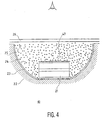
- FIG 4 shows another embodiment 40 of the present invention.
- Figure 4 is identical to Fig. 2 except that a UV/blue transmitting and visible light reflecting filter 47 is added directly to the top of the LED stack 21.
- This is also a short-wave-pass (SWP) filter, although it is placed at a different position and has a different function than the SWP filter 27 described in embodiment 3.
- SWP short-wave-pass
- the use of the SWP filter directly on the top of the LED stack has the advantage that visible light emitted by the phosphor grains in the direction of the LED stack is reflected by this filter towards the viewing side. This visible light thus does not have to pass through the LED stack twice, which would always lead to some increased losses.
- the overall intensity is thus increased at the cost of a slightly more complicated structure.
- embodiments are the combinations of embodiment 7 with the UV/blue absorbing glass plate on the top, and with this glass plate provided with a filter, which may be either a LWP filter, a SWP filter or a bandpass filter.
- a filter which may be either a LWP filter, a SWP filter or a bandpass filter.
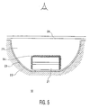
- the afore described preferred embodiments of the invention are particularly suitable when the wavelength of the UV/blue light is not too short, for example above 390 nm.
- shorter wavelengths in the range from 360 to 390 nm, in particular close to 360 nm, it is more difficult to find a UV resistant epoxy.
- the cup shaped header 22 may then be filled with epoxy 25, which is still as resistant as possible for UV/blue light. All further additions as described in embodiments 1 to 13 then be applied.
Abstract
Description
- This invention relates to light emitting devices comprising a UV/blue-emitting light emitting diode (LED) and a UV/blue-excitable, visible light emitting phosphor. Such light emitting devices are disclosed in
Japanese Kokai No. 5-152609 WO 97/48138 - As used herein, the term "UV/blue LED" means an LED emitting in the UV range, or in the blue range, or in both the UV and blue ranges of the electromagnetic spectrum.
- Visible light emitting diodes (LED's) are well known. These are multilayer epitaxial structures based mainly on AlGaAs and InGaAlP as basic materials. In these LED's the light is generated in an active region having a refractive index n of about 3.5, and emitted with an isotropic angular distribution.-The light then has to pass interfaces to exit the LED. Such LED's are typically encapsulated in an epoxy with refractive index n of about 1.5. Application of Snell's law shows that only light emitted from the active region within an angle theta of about 0.443 radians to the normal of the interface with the epoxy can exit from the top of the LED stack. For larger angles there is total internal reflection. This means that only a fraction (1- cos(theta)), hence 9.6 %, of the light can be used.
- This problem has been recognized and the efficiency of visible LED's has been enhanced significantly by reflecting visible light emitted from the sides of the LED stack, so called edge light, towards the viewing side. The edge emission of LED's is especially important when internal losses are low so that light internally reflected from the top or bottom of the LED stack can escape from the edges without too much absorption. The subsequent escape of visible light from the epoxy to air is done in a relatively efficient way by shaping the
epoxy 11 in the form of adome 12 with relatively large dimensions compared to the dimensions of theLED stack 13 and the cup-shaped header 14 in which the LED is placed, as is illustrated in Fig. 1. - Because of this large dimension most of the top and edge light coming from the LED has a small angle with the normal when arriving at the dome-air interface, and most of this light will thus be transmitted.
- Because of recent advances in GaN-based epitaxial devices, it has become possible to make UV/blue lasers as well as UV/blue LED's, For some applications, conversion of UV/blue light from an LED to visible (e.g. red, green, blue or white) light using phosphors may be more attractive than the direct application of visible LED's. Such UV/blue-LED phosphor devices, for example, offer the opportunity to encompass a wider color range, which is important for display as well as for illumination applications.
-
JP 07 099 345 A -
GB 1 332 462 - Successful implementation of such device applications is of course dependent upon the efficient conversion of UV/blue light into visible light and the subsequent efficient extraction of the generated visible light from the device.
- Accordingly, it is an object of the invention to enhance this efficient conversion and extraction of light from a UV/blue LED-phosphor device.
- It is another object of the invention to modify the spectral distribution of the emitted light from such a device.
- In GaN-based UV/blue LED's, the UV/blue light is generated in an active region having a refractive index of about 2.5, significantly below the earlier quoted value of 3.5 for visible LED's based on GaAs. The angular distribution of this light is also isotropic. Because of this lower refractive index, one might think that a much larger fraction of UV/blue light will be emitted through the top of the stack into the epoxy, and that edge light will thus be much less important.
- However, application of Snell's law shows that only light emitted in the active region within an angle theta = 0.644 radians to the normal of the interface with the epoxy can ultimately exit from the top of the LED into the epoxy. For larger angles there still is total internal reflection. This means that in this case a fraction (1 - cos(theta)), hence still only about 20%, of the light can be used. Thus, about 80% of the generated UV/blue is lost, so that edge light may still be important when the absorption of UV/blue in the LED stack is relatively small.
- Accordingly, a first aspect of the invention is to use a major part of the edge light in such a device by the use and appropriate positioning of reflectors and phosphor.
- A second aspect of the invention is to affect the angular emission and the color of the visible light emitted by the UV/blue LED-phosphor device by the use of one or more dielectric filters in the device.
- In accordance with the invention, a light emitting device for use in lighting and/or display applications includes a UV/blue LED located in a depression having reflecting sidewalls, a light transmitting material surrounding the LED and filling the depression, and a phosphor in the form of particles either dispersed in the light transmitting material or adhered to the surface of the LED. The sidewalls reflect UV/blue as well as visible light, thus enhancing the efficiency of the device.
- Optical filters located on the top of the LED and/or the bottom of a UV/blue absorbing glass plate covering the depression further enhance efficiency and/or spectral characteristics of the emitted light. For example, in a two dimensional array of such LED's, an associated array of color filters can be used to convert white light to colored light, or to enhance the color purity of colored light.
- The invention will be explained and illustrated in terms of a number of embodiments, with the help of the drawings, in which:
- Fig. 1a is a schematic diagram of a visible light emitting device of the prior art employing a visible LED;
- Fig. 1b is a detailed view of the LED in the device of Fig. 1a;
- Figs. 2 is a schematic diagram of a portion of a UV/blue LED-phosphor device useful for understanding the invention; and
- Figs. 3 to 5 are diagrams similar to that of Fig. 2 illustrating embodiments of the invention.
- The UV/blue LED's employed in the light emitting devices of the invention are similar in structure to those of visible LED's of the type shown in Fig. 1b, ie, such structures include at a minimum a lower
ohmic contact layer 1, asubstrate 2, anactive layer 4 sandwiched between lower and upper wide band gap confining layers 3 and 5, a wide band gap injection/window layer 5, and an upperohmic contact layer 6. However, UV/blue LED's are based on GaN and its alloys, instead of GaAs and its alloys. Such LED's may include one or more additional layers, such as guiding layers and buffer layers. In addition, the injection/window layer may itself be a multilayer structure, having a graded band gap. - A more detailed description of such GaN-based LED's may be found in
WO 97/48138 - Referring now to Fig. 2, a
device 20 includes UV/blue-LED stack 21, which is placed in a (e.g. plastic) cup-shaped header 22, similar to theheader 14 shown in Fig. 1a. Provided on the inside of the cup is amirror 23 which reflects both the UV/blue light generated by theLED 21 as well as the visible light generated by thephosphor 24. When the viewing side is called the front side, the feedthroughs with electrical connections can be on the back side, in a manner similar to that shown in Fig. 1. - Specifically, the header in Fig. 1 is divided by
insulating region 17 into two conductingportions LED stack 13 makes contact withportion 14a via lowerohmic contact layer 1, whilelead wire 7 connectsportion 14b with upperohmic contact layer 6. - The cup is filled with
transparent material 25, preferably a UV/blue light resistant epoxy such as a cycloaliphatic epoxy, through which thephosphor 24 is mixed homogeneously. The product of phosphor grain density and grain size should be made high enough to ensure that most of the UV/blue light is converted to visible light. To prevent UV/blue light which is not absorbed by the phosphor grains from exiting into air, absorber 26 a small flat glass plate can be placed on the top of the cup-shaped header. Edge light which is not absorbed by thephosphor grains 24 will be reflected bymirror 23 back for another opportunity to be absorbed. Thus, the efficiency of the device is enhanced. - An advantage of mixing the phosphor grains through the epoxy is that the number of processing steps is reduced compared to the case when phosphor layers are deposited separately. The latter would involve deposition with a binder and a separate baking step to get rid of the binder material. When necessary, the phosphor grains can be provided with a protective coating to avoid possible reactions between phosphor grains and the epoxy.
- The phosphor grains in the embodiment of Fig. 2 can be either of one phosphor emitting one color (broadband, narrow band or multi line, e.g. red, green, blue, yellow or white), or a mixture of phosphor grains emitting different colors, to get a good color rendering.
- The visible light will be emitted isotropically within the epoxy. Upon exiting from the epoxy to air there is a transition from n = 1.5 to n = 1.0. Applying Snell's law again we find that only visible light emitted in the n = 1.5 material within an angle theta = 0.730 radians to the normal of the interface can exit into the air with n = 1.0. For larger angles there is total internal reflection. This means that a fraction (1 - cos(theta)), hence still only 25.6 % of the light can be extracted.
- However, most phosphors have a refractive index of 2 or larger. With an epoxy which is highly transparent and which has a significantly smaller refractive index than the phosphor grains, this means that the back-reflected light will be (multiply) scattered by the phosphor grains. Part of this will be redistributed to angles within the 0.730 radians to the normal and can then exit into air. By thus ensuring a sufficiently different refractive index of epoxy and phosphor, the emission of visible light into air is enhanced by this angular redistribution. Roughening the outer surface of the epoxy may also be used to change the angles of incidence of the light on the epoxy-air interface and to enhance the overall light emission.
- Figure 2 thus shows a
device 1 in which efficient use is made of edge UV/blue light and in which the generated visible light is also collected in an efficient way. The UV/visible light mirror on the inside of the cup makes a major contribution to the efficient use of both UV and visible light. - The UV/blue LED-phosphor device shown in Fig. 2 employing a single LED can be used alone or together with other such devices. For example, such devices can be arranged in 1- or 2-dimensional arrays, with each separate LED in a cup with internal mirror and filled with epoxy and phosphor. Furthermore, one can also make an LED stack which is much longer in one direction, for example the y-direction (normal to the plane of the Figure) than in the other (the x-) direction. In that case, the cup would become a channel of sufficient length to accommodate the elongated LED. Such an elongated device can be used alone or in an array, for example, in combination with a transparent slab as a UV/blue back light for one of the LCD displays described by Vriens in
US Patent 4,822,144 . - Such an elongated LED, having for example, a length-to-width ratio of 2 or more, is expected to have a more efficient light extraction and thermal conductivity than an LED of the same area having a ratio near unity.
-
Device 2 is similar todevice 1, with the difference that the LED-cup combination, with the cup filled with the phosphor-epoxy mixture, is encapsulated in a transparent epoxy with much larger dimensions and with a dome-shaped top, in essentially the same way as shown in Fig. 1. This gives an epoxy-air interface which lies much farther from the region where the visible light is generated and results in much smaller angles of incidence of the light to the normal on the epoxy-air interface. These smaller angles in turn lead to a much enhanced transmission of the light through this interface and to a more narrow angular distribution of the emitted light. - The epoxy used for encapsulation does not contain phosphor material and need not be of the same type as the epoxy used for filling the cup. The small glass plate used for UV protection may be positioned between the two epoxies.
-
Device 2 can be used, and should preferably be used, in the case of either application of single LED's or when more LED's are used in 1- or 2-dimensional arrays, when the application allows the use of a relatively large spacing between the separate LED's. The use of larger spacings between the individual LED's is advantageous for reducing heating problems. - Figure 3 shows a
first embodiment 30 of the present invention. Figure 3 is the same as Fig. 2, except that a long-wave pass (LWP)filter 27 is added, positioned on the front (viewing) side of theLED stack 21. This LWP filter can be made, for example, by evaporation or sputtering onto theglass plate 26, which is then used as before for additional UV protection. The preferred LWP filters are multilayer dielectric stacks with alternatingly high and low refractive index. The functions of the LWP filter are: (1) to reflect UV/blue light back to the phosphor and (2) to transmit visible light emitted by the phosphor. This ensures a better absorption of the UV/blue by the phosphor and also makes it possible to reduce the phosphor grain density somewhat. This in turn enhances the transmission of the visible light. Furthermore, the reflection of UV/blue gives a protection for the epoxy which may be used for encapsulation and gives a protection for the viewers. The overall result is a more efficient use of both the UV and visible light and a better UV protection. -
Embodiment 2 is similar toembodiment 1, with the difference that the LED-cup combination, with the cup filled with the phosphor-epoxy mixture and on the top the glass plate with LWP filter, is encapsulated in a transparent epoxy with much larger dimensions and with the dome on the top in the same way as shown in Fig. 1. This again gives an interface to air which lies much farther from the region where the visible light is generated and thus results again in smaller angles of incidence with respect to the normal, of the visible light on the interface to air. - These smaller angles of incidence lead to an enhanced transmission of light through this interface and to a more narrow overall angular distribution of the emitted light.
- Embodiment 3 is the same as
embodiment 1 except that instead of a long-wave-pass filter, a short-wave pass (SWP)filter 27 is added on the front (viewing) side of theLED stack 21. This SWP filter can also be made, for example, by evaporation or sputtering onto the afore mentioned glass plate. Theglass plate 26 is then used as before for UV protection. - The preferred SWP filters are multilayer dielectric stacks with alternatingly high and low refractive index and with preferably at least 12 layers, most of these of the so called quarter-wave type. For different devices, projection TV tubes in particular, such SWP filters have been described in Vriens et al.
US Patents 4,634,926 ;4,647,812 and4,882,617 . These filters can be used for UV/blue LED-phosphor devices provided with a one-color (for example red, green or blue) phosphor which emits broadband or multi-line light, as usual for phosphors. The functions of the SWP filter are: (1) to reflect light of too long wavelength and (2) to reflect part of the light of the wanted wavelengths. Without the filter, this latter light exits into air at both small and large angles to the normal (with the so-called Lambertian or cosine distribution). With the filter, the large-angle light is reflected by the filter and subsequently multiply scattered, angularly redistributed and back-reflected by the phosphor grains to the filter. A significant part of this light can then exit into air at small angles to the normal on the surface. The overall result is a more narrow angular distribution with up to a factor of 2 gain in light intensity in the forward direction, and furthermore a more saturated (i.e. more pure) color. For applications where a more directed beam of light is needed, for example, in optical systems with a relatively small collection angle, this is an advantage. More saturated colors enhance the visibility. For applications such as traffic lights both these advantages may be important. For a different application, projection TV, the functioning of these short-wave pass interference filters in combination with a phosphor layer is explained in detail by Vriens et al. in Philips Technical Review, Vol. 44, . -
Embodiment 4 is the same as embodiment 3 except that the LED-cup combination is encapsulated in a transparent epoxy with much larger dimensions and with a domed top in the same way as shown in Fig. 1. - Embodiment 5 is a preferred embodiment which combines the advantages of
embodiments 1 and 3. This is achieved by using a bandpass (BP) interference filter in place of the afore described LWP and SWP filters on the front (viewing) side of theLED stack 21. On the short-wavelength side this BP filter has the characteristics of the LWP filter, ie, it reflects UV/blue and transmits visible light. On the long-wavelength side it has the characteristics of the SWP filter, ie, it reflects visible light of too long wavelengths at all angles and it reflects visible light of shorter wavelengths at large angles. - The preferred band pass filters are also multilayer dielectric stacks with alternately high and low refractive index, also with preferably at least 12 layers, with a slightly different thickness distribution from that of the SWP filter.
-
Embodiment 6 is the same as embodiment 5 except that the LED-cup combination is encapsulated in a transparent epoxy with much larger dimensions and with a domed top in the same way as shown in Fig. 1. - Figure 4 shows another
embodiment 40 of the present invention. Figure 4 is identical to Fig. 2 except that a UV/blue transmitting and visiblelight reflecting filter 47 is added directly to the top of theLED stack 21. This is also a short-wave-pass (SWP) filter, although it is placed at a different position and has a different function than theSWP filter 27 described in embodiment 3. The use of the SWP filter directly on the top of the LED stack has the advantage that visible light emitted by the phosphor grains in the direction of the LED stack is reflected by this filter towards the viewing side. This visible light thus does not have to pass through the LED stack twice, which would always lead to some increased losses. - The overall intensity is thus increased at the cost of a slightly more complicated structure.
- These embodiments are the combinations of
embodiment 7 with the UV/blue absorbing glass plate on the top, and with this glass plate provided with a filter, which may be either a LWP filter, a SWP filter or a bandpass filter. - These are embodiments 8 to 10 with the encapsulation in epoxy with larger dimensions and with the dome shape on the top.
- The afore described preferred embodiments of the invention are particularly suitable when the wavelength of the UV/blue light is not too short, for example above 390 nm. When shorter wavelengths are used, in the range from 360 to 390 nm, in particular close to 360 nm, it is more difficult to find a UV resistant epoxy. In that case it may be advantageous to deposit the
phosphor grains 54 as close as possible to theLED stack 21, as illustrated in the preferred embodiment shown in Fig. 5. The cup shapedheader 22 may then be filled withepoxy 25, which is still as resistant as possible for UV/blue light. All further additions as described inembodiments 1 to 13 then be applied. - The invention has necessarily been described in terms of a limited number of embodiments and variations thereof. Other embodiments and variations of embodiments will become apparent to those skilled in the art, and are intended to be encompassed within the scope of the appended claims.
Claims (13)
- A visible light emitting device (30; 40; 50) comprising: a supporting body (22) having an upper surface with a depression having an opening in the upper surface; a UV/blue and visible light-reflecting layer (23) on the surface of the depression; a UV/blue light emitting diode (21) centrally located on the light reflecting layer (23); the LED (21) having an active region with a first index of refraction; particles (24; 54) of a visible light emitting phosphor surrounding the sides and top of the LED (21); and a UV/blue and visible light transmitting material (25) surrounding the LED (21) and filling the depression, the UV/blue and visible light transmitting material (25) having a second index of refraction lower than the said first index of refraction, characterized in that
a filter (27), selected from the group consisting of a long-wave pass filter, a short-wave pass filter and a band pass filter, is arranged over the upper surface of the LED (21). - The visible light emitting device of claim 1 in which said filter (27) is a long-wave pass filter.
- The visible light emitting device of claim 1 in which said filter (27) is a short-wave pass filter.
- The visible light emitting device of claim 1 in which said filter (27) is a band pass filter.
- The visible light emitting device of any of the preceding claims in which a UV/blue light-absorbing, visible-light transmitting plate (26) covers the opening of the depression.
- The visible light emitting device of claim 5, in which said filter (27) is located on the lower surface of said plate (26).
- The visible light emitting device of any of the preceding claims, in which said filter (27) comprises a multilayer dielectric stack with alternating high and low refracting index.
- The visible light emitting device of any of the preceding claims, in which the phosphor particles (24) are dispersed in the UV and visible light transmitting material.
- The visible light emitting device of any of the claims 1 to 7, in which the phosphor particles (54) are adhered to the sides and top of the LED (21).
- The visible light emitting device of claim 6 in which a further SWP filter (47) is located directly on the upper surface of the LED (21).
- The visible light emitting device of claim 1 in which the LED (21) is elongated in one direction parallel to the plane of the top surface of the LED (21), and in which the depression is channel-shaped, with a length dimension sufficient to accommodate the LED.
- A display device comprising a light source and an electro-optic light modulator, in which the light source comprises an array of visible light emitting devices of the type claimed in claim 1.
- A visible light emitting device (30; 40; 50) comprising: a supporting body (22) having an upper surface with a depression having an opening in the upper surface; a UV/blue and visible light-reflecting layer (23) on the surface of the depression; a UV/blue light emitting diode (21) centrally located on the light reflecting layer (23); the LED (21) having an active region with a first index of refraction; particles (24; 54) of a visible light emitting phosphor surrounding the sides and top of the LED (21); and a UV/blue and visible light transmitting material (25) surrounding the LED (21) and filling the depression, the UV/blue and visible light transmitting material (25) having a second index of refraction lower than the said first index of refraction, characterized in that
a SWP filter (47) is located directly on the upper surface of the LED (21).
Applications Claiming Priority (3)
| Application Number | Priority Date | Filing Date | Title |
|---|---|---|---|
| US08/863,987 US5813753A (en) | 1997-05-27 | 1997-05-27 | UV/blue led-phosphor device with efficient conversion of UV/blues light to visible light |
| US863987 | 1997-05-27 | ||
| PCT/IB1998/000729 WO1998054929A2 (en) | 1997-05-27 | 1998-05-14 | Uv/blue led-phosphor device with efficient conversion of uv/blue light to visible light |
Publications (2)
| Publication Number | Publication Date |
|---|---|
| EP0922305A2 EP0922305A2 (en) | 1999-06-16 |
| EP0922305B1 true EP0922305B1 (en) | 2007-08-08 |
Family
ID=25342266
Family Applications (1)
| Application Number | Title | Priority Date | Filing Date |
|---|---|---|---|
| EP98917519A Expired - Lifetime EP0922305B1 (en) | 1997-05-27 | 1998-05-14 | Uv/blue led-phosphor device with efficient conversion of uv/blue light to visible light |
Country Status (5)
| Country | Link |
|---|---|
| US (1) | US5813753A (en) |
| EP (1) | EP0922305B1 (en) |
| JP (1) | JP4173556B2 (en) |
| DE (1) | DE69838207T2 (en) |
| WO (1) | WO1998054929A2 (en) |
Cited By (39)
| Publication number | Priority date | Publication date | Assignee | Title |
|---|---|---|---|---|
| WO2009107056A2 (en) | 2008-02-28 | 2009-09-03 | Philips Intellectual Property & Standards Gmbh | Light emitting diode device |
| US7926975B2 (en) | 2007-12-21 | 2011-04-19 | Altair Engineering, Inc. | Light distribution using a light emitting diode assembly |
| US7938562B2 (en) | 2008-10-24 | 2011-05-10 | Altair Engineering, Inc. | Lighting including integral communication apparatus |
| US7946729B2 (en) | 2008-07-31 | 2011-05-24 | Altair Engineering, Inc. | Fluorescent tube replacement having longitudinally oriented LEDs |
| US7976196B2 (en) | 2008-07-09 | 2011-07-12 | Altair Engineering, Inc. | Method of forming LED-based light and resulting LED-based light |
| US8118447B2 (en) | 2007-12-20 | 2012-02-21 | Altair Engineering, Inc. | LED lighting apparatus with swivel connection |
| US8214084B2 (en) | 2008-10-24 | 2012-07-03 | Ilumisys, Inc. | Integration of LED lighting with building controls |
| US8256924B2 (en) | 2008-09-15 | 2012-09-04 | Ilumisys, Inc. | LED-based light having rapidly oscillating LEDs |
| CN102664230A (en) * | 2012-05-29 | 2012-09-12 | 邓崛 | LED (light emitting diode) lighting device and manufacturing method thereof |
| US8299695B2 (en) | 2009-06-02 | 2012-10-30 | Ilumisys, Inc. | Screw-in LED bulb comprising a base having outwardly projecting nodes |
| US8324817B2 (en) | 2008-10-24 | 2012-12-04 | Ilumisys, Inc. | Light and light sensor |
| US8330381B2 (en) | 2009-05-14 | 2012-12-11 | Ilumisys, Inc. | Electronic circuit for DC conversion of fluorescent lighting ballast |
| US8360599B2 (en) | 2008-05-23 | 2013-01-29 | Ilumisys, Inc. | Electric shock resistant L.E.D. based light |
| US8362710B2 (en) | 2009-01-21 | 2013-01-29 | Ilumisys, Inc. | Direct AC-to-DC converter for passive component minimization and universal operation of LED arrays |
| US8421366B2 (en) | 2009-06-23 | 2013-04-16 | Ilumisys, Inc. | Illumination device including LEDs and a switching power control system |
| US8444292B2 (en) | 2008-10-24 | 2013-05-21 | Ilumisys, Inc. | End cap substitute for LED-based tube replacement light |
| US8454193B2 (en) | 2010-07-08 | 2013-06-04 | Ilumisys, Inc. | Independent modules for LED fluorescent light tube replacement |
| US8523394B2 (en) | 2010-10-29 | 2013-09-03 | Ilumisys, Inc. | Mechanisms for reducing risk of shock during installation of light tube |
| US8541958B2 (en) | 2010-03-26 | 2013-09-24 | Ilumisys, Inc. | LED light with thermoelectric generator |
| US8540401B2 (en) | 2010-03-26 | 2013-09-24 | Ilumisys, Inc. | LED bulb with internal heat dissipating structures |
| US8556452B2 (en) | 2009-01-15 | 2013-10-15 | Ilumisys, Inc. | LED lens |
| US8596813B2 (en) | 2010-07-12 | 2013-12-03 | Ilumisys, Inc. | Circuit board mount for LED light tube |
| US8653984B2 (en) | 2008-10-24 | 2014-02-18 | Ilumisys, Inc. | Integration of LED lighting control with emergency notification systems |
| US8664880B2 (en) | 2009-01-21 | 2014-03-04 | Ilumisys, Inc. | Ballast/line detection circuit for fluorescent replacement lamps |
| US8674626B2 (en) | 2008-09-02 | 2014-03-18 | Ilumisys, Inc. | LED lamp failure alerting system |
| US8870415B2 (en) | 2010-12-09 | 2014-10-28 | Ilumisys, Inc. | LED fluorescent tube replacement light with reduced shock hazard |
| US8901823B2 (en) | 2008-10-24 | 2014-12-02 | Ilumisys, Inc. | Light and light sensor |
| US9057493B2 (en) | 2010-03-26 | 2015-06-16 | Ilumisys, Inc. | LED light tube with dual sided light distribution |
| US9072171B2 (en) | 2011-08-24 | 2015-06-30 | Ilumisys, Inc. | Circuit board mount for LED light |
| US9163794B2 (en) | 2012-07-06 | 2015-10-20 | Ilumisys, Inc. | Power supply assembly for LED-based light tube |
| US9184518B2 (en) | 2012-03-02 | 2015-11-10 | Ilumisys, Inc. | Electrical connector header for an LED-based light |
| US9271367B2 (en) | 2012-07-09 | 2016-02-23 | Ilumisys, Inc. | System and method for controlling operation of an LED-based light |
| US9267650B2 (en) | 2013-10-09 | 2016-02-23 | Ilumisys, Inc. | Lens for an LED-based light |
| US9285084B2 (en) | 2013-03-14 | 2016-03-15 | Ilumisys, Inc. | Diffusers for LED-based lights |
| US9401468B2 (en) | 2014-12-24 | 2016-07-26 | GE Lighting Solutions, LLC | Lamp with LED chips cooled by a phase transformation loop |
| US9510400B2 (en) | 2014-05-13 | 2016-11-29 | Ilumisys, Inc. | User input systems for an LED-based light |
| US9574717B2 (en) | 2014-01-22 | 2017-02-21 | Ilumisys, Inc. | LED-based light with addressed LEDs |
| DE102016106851A1 (en) * | 2016-04-13 | 2017-10-19 | Osram Opto Semiconductors Gmbh | Light-emitting component |
| US10161568B2 (en) | 2015-06-01 | 2018-12-25 | Ilumisys, Inc. | LED-based light with canted outer walls |
Families Citing this family (513)
| Publication number | Priority date | Publication date | Assignee | Title |
|---|---|---|---|---|
| US6041345A (en) * | 1996-03-08 | 2000-03-21 | Microsoft Corporation | Active stream format for holding multiple media streams |
| DE19638667C2 (en) | 1996-09-20 | 2001-05-17 | Osram Opto Semiconductors Gmbh | Mixed-color light-emitting semiconductor component with luminescence conversion element |
| KR20040111701A (en) | 1996-06-26 | 2004-12-31 | 지멘스 악티엔게젤샤프트 | Light-emitting semiconductor component with luminescence conversion element |
| US6274890B1 (en) * | 1997-01-15 | 2001-08-14 | Kabushiki Kaisha Toshiba | Semiconductor light emitting device and its manufacturing method |
| WO1998039805A1 (en) * | 1997-03-03 | 1998-09-11 | Koninklijke Philips Electronics N.V. | White light-emitting diode |
| US6623670B2 (en) | 1997-07-07 | 2003-09-23 | Asahi Rubber Inc. | Method of molding a transparent coating member for light-emitting diodes |
| US20030133292A1 (en) | 1999-11-18 | 2003-07-17 | Mueller George G. | Methods and apparatus for generating and modulating white light illumination conditions |
| US7014336B1 (en) | 1999-11-18 | 2006-03-21 | Color Kinetics Incorporated | Systems and methods for generating and modulating illumination conditions |
| US5962971A (en) * | 1997-08-29 | 1999-10-05 | Chen; Hsing | LED structure with ultraviolet-light emission chip and multilayered resins to generate various colored lights |
| US5982092A (en) * | 1997-10-06 | 1999-11-09 | Chen; Hsing | Light Emitting Diode planar light source with blue light or ultraviolet ray-emitting luminescent crystal with optional UV filter |
| US6252254B1 (en) * | 1998-02-06 | 2001-06-26 | General Electric Company | Light emitting device with phosphor composition |
| US6469322B1 (en) | 1998-02-06 | 2002-10-22 | General Electric Company | Green emitting phosphor for use in UV light emitting diodes |
| US6294800B1 (en) * | 1998-02-06 | 2001-09-25 | General Electric Company | Phosphors for white light generation from UV emitting diodes |
| US6068383A (en) * | 1998-03-02 | 2000-05-30 | Robertson; Roger | Phosphorous fluorescent light assembly excited by light emitting diodes |
| JPH11321455A (en) * | 1998-05-12 | 1999-11-24 | Toyoda Gosei Co Ltd | Interior lighting system |
| JP3410024B2 (en) * | 1998-06-18 | 2003-05-26 | 富士通株式会社 | Gas discharge display |
| JP2000036201A (en) * | 1998-07-06 | 2000-02-02 | Fukukoku Ko | Light emission method and light emission device generating different visible electromagnetic wave length by exciting electron in covering layer molecules |
| US6160273A (en) * | 1998-07-15 | 2000-12-12 | Xerox Corporation | Diode pumped solid state edge emitting light source |
| JP3785820B2 (en) * | 1998-08-03 | 2006-06-14 | 豊田合成株式会社 | Light emitting device |
| US5959316A (en) * | 1998-09-01 | 1999-09-28 | Hewlett-Packard Company | Multiple encapsulation of phosphor-LED devices |
| US6366018B1 (en) * | 1998-10-21 | 2002-04-02 | Sarnoff Corporation | Apparatus for performing wavelength-conversion using phosphors with light emitting diodes |
| US6404125B1 (en) * | 1998-10-21 | 2002-06-11 | Sarnoff Corporation | Method and apparatus for performing wavelength-conversion using phosphors with light emitting diodes |
| US6204523B1 (en) * | 1998-11-06 | 2001-03-20 | Lumileds Lighting, U.S., Llc | High stability optical encapsulation and packaging for light-emitting diodes in the green, blue, and near UV range |
| US6299338B1 (en) | 1998-11-30 | 2001-10-09 | General Electric Company | Decorative lighting apparatus with light source and luminescent material |
| US6429583B1 (en) | 1998-11-30 | 2002-08-06 | General Electric Company | Light emitting device with ba2mgsi2o7:eu2+, ba2sio4:eu2+, or (srxcay ba1-x-y)(a1zga1-z)2sr:eu2+phosphors |
| US6373188B1 (en) * | 1998-12-22 | 2002-04-16 | Honeywell International Inc. | Efficient solid-state light emitting device with excited phosphors for producing a visible light output |
| US6329676B1 (en) * | 1999-03-01 | 2001-12-11 | Toru Takayama | Flat panel solid state light source |
| US6155699A (en) * | 1999-03-15 | 2000-12-05 | Agilent Technologies, Inc. | Efficient phosphor-conversion led structure |
| JP2000269551A (en) * | 1999-03-18 | 2000-09-29 | Rohm Co Ltd | Chip-type light emitting device |
| KR100556475B1 (en) * | 1999-04-01 | 2006-03-03 | 엘지전자 주식회사 | Plasma Display Panel |
| TW455908B (en) * | 1999-04-20 | 2001-09-21 | Koninkl Philips Electronics Nv | Lighting system |
| JP2001144331A (en) | 1999-09-02 | 2001-05-25 | Toyoda Gosei Co Ltd | Light-emitting device |
| US6504301B1 (en) | 1999-09-03 | 2003-01-07 | Lumileds Lighting, U.S., Llc | Non-incandescent lightbulb package using light emitting diodes |
| US6696703B2 (en) | 1999-09-27 | 2004-02-24 | Lumileds Lighting U.S., Llc | Thin film phosphor-converted light emitting diode device |
| KR100683364B1 (en) | 1999-09-27 | 2007-02-15 | 필립스 루미리즈 라이팅 캄파니 엘엘씨 | A light emitting diode device that produces white light by performing complete phosphor conversion |
| US6686691B1 (en) | 1999-09-27 | 2004-02-03 | Lumileds Lighting, U.S., Llc | Tri-color, white light LED lamps |
| EP1089069A3 (en) * | 1999-10-01 | 2001-08-29 | CorkOpt Limited | Linear illumination |
| US6676279B1 (en) | 1999-10-04 | 2004-01-13 | David A. Hubbell | Area lighting device using discrete light sources, such as LEDs |
| DE19952932C1 (en) * | 1999-11-03 | 2001-05-03 | Osram Opto Semiconductors Gmbh | LED white light source with broadband excitation |
| US20020176259A1 (en) * | 1999-11-18 | 2002-11-28 | Ducharme Alfred D. | Systems and methods for converting illumination |
| US8829546B2 (en) * | 1999-11-19 | 2014-09-09 | Cree, Inc. | Rare earth doped layer or substrate for light conversion |
| US7202506B1 (en) * | 1999-11-19 | 2007-04-10 | Cree, Inc. | Multi element, multi color solid state LED/laser |
| US6357889B1 (en) * | 1999-12-01 | 2002-03-19 | General Electric Company | Color tunable light source |
| US6513949B1 (en) * | 1999-12-02 | 2003-02-04 | Koninklijke Philips Electronics N.V. | LED/phosphor-LED hybrid lighting systems |
| US6666567B1 (en) * | 1999-12-28 | 2003-12-23 | Honeywell International Inc. | Methods and apparatus for a light source with a raised LED structure |
| DE19963805B4 (en) | 1999-12-30 | 2005-01-27 | Osram Opto Semiconductors Gmbh | White light source based on non-linear optical processes |
| DE19964252A1 (en) * | 1999-12-30 | 2002-06-06 | Osram Opto Semiconductors Gmbh | Surface mount component for an LED white light source |
| US8093823B1 (en) | 2000-02-11 | 2012-01-10 | Altair Engineering, Inc. | Light sources incorporating light emitting diodes |
| US7049761B2 (en) | 2000-02-11 | 2006-05-23 | Altair Engineering, Inc. | Light tube and power supply circuit |
| EP1264298B1 (en) * | 2000-03-06 | 2007-01-03 | Teledyne Lighting and Display Products, Inc. | Led light source with field-of-view-controlling optics |
| JP2003526190A (en) | 2000-03-06 | 2003-09-02 | テレダイン ライティング アンド ディスプレイ プロダクツ, インコーポレイテッド | Lighting device having quantum dot layer |
| US6409938B1 (en) | 2000-03-27 | 2002-06-25 | The General Electric Company | Aluminum fluoride flux synthesis method for producing cerium doped YAG |
| US6538371B1 (en) | 2000-03-27 | 2003-03-25 | The General Electric Company | White light illumination system with improved color output |
| US6522065B1 (en) * | 2000-03-27 | 2003-02-18 | General Electric Company | Single phosphor for creating white light with high luminosity and high CRI in a UV led device |
| US6867542B1 (en) * | 2000-03-29 | 2005-03-15 | General Electric Company | Floating chip photonic device and method of manufacture |
| US6501100B1 (en) | 2000-05-15 | 2002-12-31 | General Electric Company | White light emitting phosphor blend for LED devices |
| US6466135B1 (en) | 2000-05-15 | 2002-10-15 | General Electric Company | Phosphors for down converting ultraviolet light of LEDs to blue-green light |
| US6555958B1 (en) | 2000-05-15 | 2003-04-29 | General Electric Company | Phosphor for down converting ultraviolet light of LEDs to blue-green light |
| US6621211B1 (en) | 2000-05-15 | 2003-09-16 | General Electric Company | White light emitting phosphor blends for LED devices |
| US6648496B1 (en) | 2000-06-27 | 2003-11-18 | General Electric Company | Nightlight with light emitting diode source |
| DE60143152D1 (en) | 2000-06-29 | 2010-11-11 | Koninkl Philips Electronics Nv | OPTOELECTRIC ELEMENT |
| DE10036940A1 (en) * | 2000-07-28 | 2002-02-07 | Patent Treuhand Ges Fuer Elektrische Gluehlampen Mbh | Luminescence conversion LED |
| US6747406B1 (en) * | 2000-08-07 | 2004-06-08 | General Electric Company | LED cross-linkable phospor coating |
| DE60137995D1 (en) * | 2000-08-09 | 2009-04-30 | Avago Technologies General Ip | Light-emitting devices |
| US6614103B1 (en) | 2000-09-01 | 2003-09-02 | General Electric Company | Plastic packaging of LED arrays |
| JP2002141556A (en) | 2000-09-12 | 2002-05-17 | Lumileds Lighting Us Llc | Light emitting diode with improved light extraction efficiency |
| JP4077170B2 (en) * | 2000-09-21 | 2008-04-16 | シャープ株式会社 | Semiconductor light emitting device |
| JP3609709B2 (en) * | 2000-09-29 | 2005-01-12 | 株式会社シチズン電子 | Light emitting diode |
| US6998281B2 (en) * | 2000-10-12 | 2006-02-14 | General Electric Company | Solid state lighting device with reduced form factor including LED with directional emission and package with microoptics |
| US6650044B1 (en) | 2000-10-13 | 2003-11-18 | Lumileds Lighting U.S., Llc | Stenciling phosphor layers on light emitting diodes |
| US6637924B2 (en) | 2000-11-15 | 2003-10-28 | Teledyne Lighting And Display Products, Inc. | Strip lighting apparatus and method |
| US6515314B1 (en) | 2000-11-16 | 2003-02-04 | General Electric Company | Light-emitting device with organic layer doped with photoluminescent material |
| US6518600B1 (en) | 2000-11-17 | 2003-02-11 | General Electric Company | Dual encapsulation for an LED |
| US20020063520A1 (en) * | 2000-11-29 | 2002-05-30 | Huei-Che Yu | Pre-formed fluorescent plate - LED device |
| AT410266B (en) * | 2000-12-28 | 2003-03-25 | Tridonic Optoelectronics Gmbh | LIGHT SOURCE WITH A LIGHT-EMITTING ELEMENT |
| MY145695A (en) * | 2001-01-24 | 2012-03-30 | Nichia Corp | Light emitting diode, optical semiconductor device, epoxy resin composition suited for optical semiconductor device, and method for manufacturing the same |
| DE10105802A1 (en) | 2001-02-07 | 2002-08-08 | Patent Treuhand Ges Fuer Elektrische Gluehlampen Mbh | Semiconductor component with reflector |
| US6541800B2 (en) | 2001-02-22 | 2003-04-01 | Weldon Technologies, Inc. | High power LED |
| JP2002261333A (en) * | 2001-03-05 | 2002-09-13 | Toyoda Gosei Co Ltd | Light-emitting device |
| US6874910B2 (en) * | 2001-04-12 | 2005-04-05 | Matsushita Electric Works, Ltd. | Light source device using LED, and method of producing same |
| US6686676B2 (en) | 2001-04-30 | 2004-02-03 | General Electric Company | UV reflectors and UV-based light sources having reduced UV radiation leakage incorporating the same |
| EP1419341A4 (en) * | 2001-05-03 | 2005-12-14 | Luminary Logic Ltd | Ultraviolet illumination of indicia |
| JP3940596B2 (en) * | 2001-05-24 | 2007-07-04 | 松下電器産業株式会社 | Illumination light source |
| US6989412B2 (en) | 2001-06-06 | 2006-01-24 | Henkel Corporation | Epoxy molding compounds containing phosphor and process for preparing such compositions |
| US6642652B2 (en) | 2001-06-11 | 2003-11-04 | Lumileds Lighting U.S., Llc | Phosphor-converted light emitting device |
| US6576488B2 (en) * | 2001-06-11 | 2003-06-10 | Lumileds Lighting U.S., Llc | Using electrophoresis to produce a conformally coated phosphor-converted light emitting semiconductor |
| US6798136B2 (en) * | 2001-06-19 | 2004-09-28 | Gelcore Llc | Phosphor embedded die epoxy and lead frame modifications |
| DE10131698A1 (en) | 2001-06-29 | 2003-01-30 | Osram Opto Semiconductors Gmbh | Surface-mountable radiation-emitting component and method for its production |
| JP2003029654A (en) * | 2001-07-11 | 2003-01-31 | Sony Corp | Display device |
| US6784603B2 (en) * | 2001-07-20 | 2004-08-31 | Teledyne Lighting And Display Products, Inc. | Fluorescent lighting apparatus |
| DE10137042A1 (en) * | 2001-07-31 | 2003-02-20 | Patent Treuhand Ges Fuer Elektrische Gluehlampen Mbh | Planar light source based on LED |
| DE10142009B4 (en) * | 2001-08-28 | 2010-04-22 | Osram Opto Semiconductors Gmbh | LED light source with a conversion agent and with a UV absorbing layer |
| US6806642B2 (en) | 2001-09-04 | 2004-10-19 | Durel Corporation | Light source with cascading dyes and BEF |
| US6599000B2 (en) * | 2001-10-15 | 2003-07-29 | Steven T. Nolan | Interior lamp for producing white light using bright white LEDs |
| DE10153259A1 (en) | 2001-10-31 | 2003-05-22 | Osram Opto Semiconductors Gmbh | Optoelectronic component |
| JP2003152227A (en) * | 2001-11-14 | 2003-05-23 | Citizen Electronics Co Ltd | Means and method for correcting color of led |
| JP2003227884A (en) * | 2001-11-29 | 2003-08-15 | Casio Comput Co Ltd | Light emission and display device and electronic apparatus |
| US6979105B2 (en) * | 2002-01-18 | 2005-12-27 | Leysath Joseph A | Light device with photonic band pass filter |
| JP4191937B2 (en) * | 2002-02-15 | 2008-12-03 | 株式会社日立製作所 | White light source and image display apparatus using the same |
| US6641284B2 (en) | 2002-02-21 | 2003-11-04 | Whelen Engineering Company, Inc. | LED light assembly |
| JP2003255344A (en) * | 2002-03-05 | 2003-09-10 | Citizen Electronics Co Ltd | Front light for color liquid crystal display |
| US6635557B2 (en) * | 2002-03-15 | 2003-10-21 | Neumann Information Systems, Inc | Halogen doped solid state materials |
| US6762432B2 (en) * | 2002-04-01 | 2004-07-13 | Micrel, Inc. | Electrical field alignment vernier |
| US6641283B1 (en) | 2002-04-12 | 2003-11-04 | Gelcore, Llc | LED puck light with detachable base |
| US6870311B2 (en) * | 2002-06-07 | 2005-03-22 | Lumileds Lighting U.S., Llc | Light-emitting devices utilizing nanoparticles |
| CA2489237A1 (en) * | 2002-06-13 | 2003-12-24 | Cree, Inc. | Semiconductor emitter comprising a saturated phosphor |
| US6841802B2 (en) | 2002-06-26 | 2005-01-11 | Oriol, Inc. | Thin film light emitting diode |
| JP2004047748A (en) | 2002-07-12 | 2004-02-12 | Stanley Electric Co Ltd | Light-emitting diode |
| EP1535299B1 (en) * | 2002-07-16 | 2009-11-18 | odelo GmbH | White led headlight |
| WO2004010472A2 (en) * | 2002-07-19 | 2004-01-29 | Microsemi Corporation | Process for fabricating, and light emitting device resulting from, a homogenously mixed powder/pelletized compound |
| JP2004083653A (en) * | 2002-08-23 | 2004-03-18 | Sharp Corp | Light emitting device, phosphor and method for producing the same |
| US7800121B2 (en) * | 2002-08-30 | 2010-09-21 | Lumination Llc | Light emitting diode component |
| US10340424B2 (en) | 2002-08-30 | 2019-07-02 | GE Lighting Solutions, LLC | Light emitting diode component |
| KR100499129B1 (en) | 2002-09-02 | 2005-07-04 | 삼성전기주식회사 | Light emitting laser diode and fabricatin method thereof |
| AU2003259444A1 (en) * | 2002-09-12 | 2004-04-30 | Koninklijke Philips Electronics N.V. | Lighting device |
| WO2004027884A1 (en) | 2002-09-19 | 2004-04-01 | Cree, Inc. | Phosphor-coated light emitting diodes including tapered sidewalls, and fabrication methods therefor |
| US6744077B2 (en) * | 2002-09-27 | 2004-06-01 | Lumileds Lighting U.S., Llc | Selective filtering of wavelength-converted semiconductor light emitting devices |
| JP3910517B2 (en) * | 2002-10-07 | 2007-04-25 | シャープ株式会社 | LED device |
| JP4294295B2 (en) * | 2002-11-06 | 2009-07-08 | 株式会社小糸製作所 | Vehicle headlamp |
| US6717362B1 (en) * | 2002-11-14 | 2004-04-06 | Agilent Technologies, Inc. | Light emitting diode with gradient index layering |
| DE10256383A1 (en) * | 2002-12-02 | 2004-06-09 | Der Kluth: Decke Und Licht Gmbh | Lighting device has transparent surface coated with ultraviolet excitable fluorescent material on the side next to the UV source |
| US6744196B1 (en) * | 2002-12-11 | 2004-06-01 | Oriol, Inc. | Thin film LED |
| TW569479B (en) * | 2002-12-20 | 2004-01-01 | Ind Tech Res Inst | White-light LED applying omnidirectional reflector |
| DE10261908B4 (en) * | 2002-12-27 | 2010-12-30 | Osa Opto Light Gmbh | Method for producing a conversion light-emitting element based on semiconductor light sources |
| US20040136179A1 (en) * | 2003-01-13 | 2004-07-15 | Lewis Edward D. | Necklace with ultraviolet illuminated fluorescent pendant |
| US7091661B2 (en) * | 2003-01-27 | 2006-08-15 | 3M Innovative Properties Company | Phosphor based light sources having a reflective polarizer |
| US7091653B2 (en) | 2003-01-27 | 2006-08-15 | 3M Innovative Properties Company | Phosphor based light sources having a non-planar long pass reflector |
| US7118438B2 (en) * | 2003-01-27 | 2006-10-10 | 3M Innovative Properties Company | Methods of making phosphor based light sources having an interference reflector |
| US7157839B2 (en) * | 2003-01-27 | 2007-01-02 | 3M Innovative Properties Company | Phosphor based light sources utilizing total internal reflection |
| CN100394619C (en) * | 2003-01-27 | 2008-06-11 | 3M创新有限公司 | Lignt emmitting device for phosphor conversion |
| US20040145289A1 (en) | 2003-01-27 | 2004-07-29 | 3M Innovative Properties Company | Phosphor based light sources having a non-planar short pass reflector and method of making |
| US7312560B2 (en) * | 2003-01-27 | 2007-12-25 | 3M Innovative Properties | Phosphor based light sources having a non-planar long pass reflector and method of making |
| US20040145312A1 (en) * | 2003-01-27 | 2004-07-29 | 3M Innovative Properties Company | Phosphor based light source having a flexible short pass reflector |
| WO2004068603A2 (en) * | 2003-01-27 | 2004-08-12 | 3M Innovative Properties Company | Phosphor based light source component and method of making |
| US7245072B2 (en) * | 2003-01-27 | 2007-07-17 | 3M Innovative Properties Company | Phosphor based light sources having a polymeric long pass reflector |
| US6936857B2 (en) * | 2003-02-18 | 2005-08-30 | Gelcore, Llc | White light LED device |
| KR20050113200A (en) * | 2003-02-26 | 2005-12-01 | 크리, 인코포레이티드 | Composite white light source and method for fabricating |
| US20040166234A1 (en) * | 2003-02-26 | 2004-08-26 | Chua Bee Yin Janet | Apparatus and method for coating a light source to provide a modified output spectrum |
| US6885033B2 (en) * | 2003-03-10 | 2005-04-26 | Cree, Inc. | Light emitting devices for light conversion and methods and semiconductor chips for fabricating the same |
| FR2852533B1 (en) * | 2003-03-20 | 2006-10-06 | Arck Electronique | HOLES DETECTION DEVICE IN CONTINUOUS BAND THREADED MATERIALS |
| US6994453B2 (en) * | 2003-03-21 | 2006-02-07 | Blanchard Randall D | Illumination device having a dichroic mirror |
| US7279832B2 (en) * | 2003-04-01 | 2007-10-09 | Innovalight, Inc. | Phosphor materials and illumination devices made therefrom |
| US20040252488A1 (en) * | 2003-04-01 | 2004-12-16 | Innovalight | Light-emitting ceiling tile |
| CN101740560B (en) * | 2003-04-01 | 2012-11-21 | 夏普株式会社 | Light-emitting apparatus, backlight apparatus, and display apparatus |
| US6903380B2 (en) | 2003-04-11 | 2005-06-07 | Weldon Technologies, Inc. | High power light emitting diode |
| KR100691143B1 (en) * | 2003-04-30 | 2007-03-09 | 삼성전기주식회사 | Light emitting diode device with multi-layered phosphor |
| US7108386B2 (en) | 2003-05-12 | 2006-09-19 | Illumitech Inc. | High-brightness LED-phosphor coupling |
| US6869812B1 (en) * | 2003-05-13 | 2005-03-22 | Heng Liu | High power AllnGaN based multi-chip light emitting diode |
| US7367691B2 (en) * | 2003-06-16 | 2008-05-06 | Industrial Technology Research Institute | Omnidirectional one-dimensional photonic crystal and light emitting device made from the same |
| US7075225B2 (en) * | 2003-06-27 | 2006-07-11 | Tajul Arosh Baroky | White light emitting device |
| US7462983B2 (en) * | 2003-06-27 | 2008-12-09 | Avago Technologies Ecbu Ip (Singapore) Pte. Ltd. | White light emitting device |
| DE10361661A1 (en) * | 2003-07-14 | 2005-03-17 | Osram Opto Semiconductors Gmbh | Light-emitting component has luminescence conversion element, filter element with nano-particles that selectively reduce radiation intensity of unwanted radiation spectral sub-region(s) by absorption |
| US20050104072A1 (en) | 2003-08-14 | 2005-05-19 | Slater David B.Jr. | Localized annealing of metal-silicon carbide ohmic contacts and devices so formed |
| US7183587B2 (en) * | 2003-09-09 | 2007-02-27 | Cree, Inc. | Solid metal block mounting substrates for semiconductor light emitting devices |
| US7029935B2 (en) * | 2003-09-09 | 2006-04-18 | Cree, Inc. | Transmissive optical elements including transparent plastic shell having a phosphor dispersed therein, and methods of fabricating same |
| US7915085B2 (en) * | 2003-09-18 | 2011-03-29 | Cree, Inc. | Molded chip fabrication method |
| JP4378242B2 (en) * | 2003-09-25 | 2009-12-02 | 株式会社小糸製作所 | Vehicle lighting |
| DE10345410A1 (en) * | 2003-09-30 | 2005-05-04 | Osram Opto Semiconductors Gmbh | radiation detector |
| US6995402B2 (en) * | 2003-10-03 | 2006-02-07 | Lumileds Lighting, U.S., Llc | Integrated reflector cup for a light emitting device mount |
| US20050077535A1 (en) * | 2003-10-08 | 2005-04-14 | Joinscan Electronics Co., Ltd | LED and its manufacturing process |
| US7045975B2 (en) * | 2003-10-14 | 2006-05-16 | Cyberlux Corporation | Apparatus and methods for providing emergency safety lighting |
| DE102004002101A1 (en) * | 2003-10-17 | 2005-05-25 | Han Shin Company Ltd. | Light emitting device uses omnidirectional reflector that receives secondary light and unconverted primary light from wavelength-converter connected to omnidirectional photonic crystal |
| US20050099808A1 (en) * | 2003-11-12 | 2005-05-12 | Cheng Tzu C. | Light-emitting device |
| JP4784966B2 (en) * | 2003-11-18 | 2011-10-05 | シャープ株式会社 | Semiconductor laser device and illumination device |
| CN100470855C (en) * | 2004-01-07 | 2009-03-18 | 松下电器产业株式会社 | LED lighting light source |
| US20050174801A1 (en) * | 2004-02-05 | 2005-08-11 | Densen Cao | Backlight |
| US20050174753A1 (en) * | 2004-02-06 | 2005-08-11 | Densen Cao | Mining light |
| US7675231B2 (en) * | 2004-02-13 | 2010-03-09 | Avago Technologies Ecbu Ip (Singapore) Pte. Ltd. | Light emitting diode display device comprising a high temperature resistant overlay |
| TWI288277B (en) * | 2004-02-20 | 2007-10-11 | Jr-Yung Liou | Flat light source with high brightness and high uniformity |
| US6924233B1 (en) * | 2004-03-19 | 2005-08-02 | Agilent Technologies, Inc. | Phosphor deposition methods |
| US7355284B2 (en) | 2004-03-29 | 2008-04-08 | Cree, Inc. | Semiconductor light emitting devices including flexible film having therein an optical element |
| US7327078B2 (en) * | 2004-03-30 | 2008-02-05 | Lumination Llc | LED illumination device with layered phosphor pattern |
| KR20130036337A (en) * | 2004-03-31 | 2013-04-11 | 오스람 옵토 세미컨덕터스 게엠베하 | Radiation detector |
| JP4317478B2 (en) * | 2004-03-31 | 2009-08-19 | 三菱化学株式会社 | Phosphor-type light emitting device and endoscope device using the same as an illumination source |
| US7517728B2 (en) * | 2004-03-31 | 2009-04-14 | Cree, Inc. | Semiconductor light emitting devices including a luminescent conversion element |
| CN101076744B (en) * | 2004-04-23 | 2010-05-12 | 光处方革新有限公司 | Optical manifold for light-emitting diodes |
| US7380962B2 (en) * | 2004-04-23 | 2008-06-03 | Light Prescriptions Innovators, Llc | Optical manifold for light-emitting diodes |
| US7819549B2 (en) * | 2004-05-05 | 2010-10-26 | Rensselaer Polytechnic Institute | High efficiency light source using solid-state emitter and down-conversion material |
| US7837348B2 (en) | 2004-05-05 | 2010-11-23 | Rensselaer Polytechnic Institute | Lighting system using multiple colored light emitting sources and diffuser element |
| US11158768B2 (en) | 2004-05-07 | 2021-10-26 | Bruce H. Baretz | Vacuum light emitting diode |
| US20060255349A1 (en) * | 2004-05-11 | 2006-11-16 | Heng Liu | High power AllnGaN based multi-chip light emitting diode |
| JP4689190B2 (en) * | 2004-05-18 | 2011-05-25 | オリンパス株式会社 | Endoscope device and endoscope adapter |
| US7339332B2 (en) * | 2004-05-24 | 2008-03-04 | Honeywell International, Inc. | Chroma compensated backlit display |
| US6956247B1 (en) * | 2004-05-26 | 2005-10-18 | Lumileds Lighting U.S., Llc | Semiconductor light emitting device including photonic band gap material and luminescent material |
| US7070300B2 (en) * | 2004-06-04 | 2006-07-04 | Philips Lumileds Lighting Company, Llc | Remote wavelength conversion in an illumination device |
| US7553683B2 (en) * | 2004-06-09 | 2009-06-30 | Philips Lumiled Lighting Co., Llc | Method of forming pre-fabricated wavelength converting elements for semiconductor light emitting devices |
| US20060044823A1 (en) * | 2004-07-02 | 2006-03-02 | Discus Dental Impressions, Inc. | Curing light having a detachable tip |
| ATE383661T1 (en) * | 2004-08-06 | 2008-01-15 | Koninkl Philips Electronics Nv | HIGH PERFORMANCE LED LAMP SYSTEM |
| US7750352B2 (en) | 2004-08-10 | 2010-07-06 | Pinion Technologies, Inc. | Light strips for lighting and backlighting applications |
| US7471040B2 (en) * | 2004-08-13 | 2008-12-30 | Avago Technologies Ecbu Ip (Singapore) Pte. Ltd. | Mixed-color light emitting diode apparatus, and method for making same |
| US7217583B2 (en) * | 2004-09-21 | 2007-05-15 | Cree, Inc. | Methods of coating semiconductor light emitting elements by evaporating solvent from a suspension |
| US7309144B2 (en) * | 2004-09-21 | 2007-12-18 | Avago Technologies Ecbu Ip (Singapore) Pte Ltd | Stacked light source |
| US7372198B2 (en) | 2004-09-23 | 2008-05-13 | Cree, Inc. | Semiconductor light emitting devices including patternable films comprising transparent silicone and phosphor |
| EP1794814A1 (en) * | 2004-09-23 | 2007-06-13 | Koninklijke Philips Electronics N.V. | Light-emitting device |
| US7370993B2 (en) * | 2004-09-28 | 2008-05-13 | Goldeneye, Inc. | Light recycling illumination systems having restricted angular output |
| US20080247172A1 (en) * | 2004-09-28 | 2008-10-09 | Goldeneye, Inc. | Light recycling illumination systems having restricted angular output |
| EP1797595B1 (en) * | 2004-09-30 | 2019-12-18 | Koninklijke Philips N.V. | Brightness enhancement of led using selective ray angular recycling |
| US20060097385A1 (en) | 2004-10-25 | 2006-05-11 | Negley Gerald H | Solid metal block semiconductor light emitting device mounting substrates and packages including cavities and heat sinks, and methods of packaging same |
| DE102005028748A1 (en) * | 2004-10-25 | 2006-05-04 | Osram Opto Semiconductors Gmbh | Electromagnetic radiation emitting semiconductor device and device package |
| US7675079B1 (en) * | 2004-10-28 | 2010-03-09 | Kley Victor B | Diamond coating of silicon-carbide LEDs |
| US7322732B2 (en) * | 2004-12-23 | 2008-01-29 | Cree, Inc. | Light emitting diode arrays for direct backlighting of liquid crystal displays |
| TWI239671B (en) * | 2004-12-30 | 2005-09-11 | Ind Tech Res Inst | LED applied with omnidirectional reflector |
| TWI245440B (en) * | 2004-12-30 | 2005-12-11 | Ind Tech Res Inst | Light emitting diode |
| JP2006190764A (en) * | 2005-01-05 | 2006-07-20 | Stanley Electric Co Ltd | Surface mounting led |
| US7821023B2 (en) | 2005-01-10 | 2010-10-26 | Cree, Inc. | Solid state lighting component |
| US9070850B2 (en) | 2007-10-31 | 2015-06-30 | Cree, Inc. | Light emitting diode package and method for fabricating same |
| US9793247B2 (en) | 2005-01-10 | 2017-10-17 | Cree, Inc. | Solid state lighting component |
| US7304694B2 (en) * | 2005-01-12 | 2007-12-04 | Cree, Inc. | Solid colloidal dispersions for backlighting of liquid crystal displays |
| JP5109226B2 (en) * | 2005-01-20 | 2012-12-26 | 豊田合成株式会社 | Light emitting device |
| US20060171152A1 (en) * | 2005-01-20 | 2006-08-03 | Toyoda Gosei Co., Ltd. | Light emitting device and method of making the same |
| TW201403859A (en) | 2005-02-18 | 2014-01-16 | Nichia Corp | Light emitting device provided with lens for controlling light distribution characteristic |
| JP2006261540A (en) * | 2005-03-18 | 2006-09-28 | Stanley Electric Co Ltd | Light emitting device |
| US20080296589A1 (en) * | 2005-03-24 | 2008-12-04 | Ingo Speier | Solid-State Lighting Device Package |
| US8449973B2 (en) * | 2005-03-29 | 2013-05-28 | Kyocera Corporation | Reflective member, light-emitting device using same and illuminating device |
| CA2614803C (en) * | 2005-04-05 | 2015-08-25 | Tir Technology Lp | Electronic device package with an integrated evaporator |
| US7234820B2 (en) * | 2005-04-11 | 2007-06-26 | Philips Lumileds Lighting Company, Llc | Illuminators using reflective optics with recycling and color mixing |
| KR20060116479A (en) * | 2005-05-10 | 2006-11-15 | 삼성전자주식회사 | Liquid crystal display |
| US8718437B2 (en) | 2006-03-07 | 2014-05-06 | Qd Vision, Inc. | Compositions, optical component, system including an optical component, devices, and other products |
| WO2006131924A2 (en) | 2005-06-07 | 2006-12-14 | Oree, Advanced Illumination Solutions Inc. | Illumination apparatus |
| US8272758B2 (en) | 2005-06-07 | 2012-09-25 | Oree, Inc. | Illumination apparatus and methods of forming the same |
| US8215815B2 (en) | 2005-06-07 | 2012-07-10 | Oree, Inc. | Illumination apparatus and methods of forming the same |
| US8669572B2 (en) * | 2005-06-10 | 2014-03-11 | Cree, Inc. | Power lamp package |
| KR101266130B1 (en) * | 2005-06-23 | 2013-05-27 | 렌슬러 폴리테크닉 인스티튜트 | Package design for producing white light with short-wavelength leds and down-conversion materials |
| KR101161383B1 (en) * | 2005-07-04 | 2012-07-02 | 서울반도체 주식회사 | Light emitting diode and method for producing the same |
| US7382091B2 (en) * | 2005-07-27 | 2008-06-03 | Lung-Chien Chen | White light emitting diode using phosphor excitation |
| US20070045800A1 (en) * | 2005-08-19 | 2007-03-01 | Brian King | Opto-coupler with high reverse breakdown voltage and high isolation potential |
| US8563339B2 (en) * | 2005-08-25 | 2013-10-22 | Cree, Inc. | System for and method for closed loop electrophoretic deposition of phosphor materials on semiconductor devices |
| TWI261378B (en) * | 2005-09-19 | 2006-09-01 | Ind Tech Res Inst | Polarized light emitting device |
| DE102005062514A1 (en) * | 2005-09-28 | 2007-03-29 | Osram Opto Semiconductors Gmbh | Multi-purpose light emitting diode incorporates selective wavelength trap |
| JP3863169B2 (en) * | 2005-10-03 | 2006-12-27 | 東芝電子エンジニアリング株式会社 | Light emitting device |
| US20070117450A1 (en) * | 2005-11-18 | 2007-05-24 | Truxes William W | Novel jack form LED lamp package and caddy |
| US7943946B2 (en) * | 2005-11-21 | 2011-05-17 | Sharp Kabushiki Kaisha | Light emitting device |
| US20070128745A1 (en) * | 2005-12-01 | 2007-06-07 | Brukilacchio Thomas J | Phosphor deposition method and apparatus for making light emitting diodes |
| CN101460779A (en) | 2005-12-21 | 2009-06-17 | 科锐Led照明技术公司 | Lighting device |
| JP2007173083A (en) * | 2005-12-22 | 2007-07-05 | Canon Inc | Light-emitting device |
| US7614759B2 (en) | 2005-12-22 | 2009-11-10 | Cree Led Lighting Solutions, Inc. | Lighting device |
| US7798678B2 (en) * | 2005-12-30 | 2010-09-21 | 3M Innovative Properties Company | LED with compound encapsulant lens |
| JP2009530798A (en) | 2006-01-05 | 2009-08-27 | イルミテックス, インコーポレイテッド | Independent optical device for directing light from an LED |
| US8264138B2 (en) | 2006-01-20 | 2012-09-11 | Cree, Inc. | Shifting spectral content in solid state light emitters by spatially separating lumiphor films |
| US8441179B2 (en) | 2006-01-20 | 2013-05-14 | Cree, Inc. | Lighting devices having remote lumiphors that are excited by lumiphor-converted semiconductor excitation sources |
| US8101961B2 (en) * | 2006-01-25 | 2012-01-24 | Cree, Inc. | Transparent ohmic contacts on light emitting diodes with growth substrates |
| US8124957B2 (en) | 2006-02-22 | 2012-02-28 | Cree, Inc. | Low resistance tunnel junctions in wide band gap materials and method of making same |
| US7737451B2 (en) * | 2006-02-23 | 2010-06-15 | Cree, Inc. | High efficiency LED with tunnel junction layer |
| EP2041478B1 (en) | 2006-03-07 | 2014-08-06 | QD Vision, Inc. | An article including semiconductor nanocrystals |
| US9874674B2 (en) | 2006-03-07 | 2018-01-23 | Samsung Electronics Co., Ltd. | Compositions, optical component, system including an optical component, devices, and other products |
| WO2007105647A1 (en) * | 2006-03-10 | 2007-09-20 | Nichia Corporation | Light emitting device |
| JP2007258486A (en) * | 2006-03-23 | 2007-10-04 | Toyota Central Res & Dev Lab Inc | White light emitting diode |
| US7675145B2 (en) * | 2006-03-28 | 2010-03-09 | Cree Hong Kong Limited | Apparatus, system and method for use in mounting electronic elements |
| US7766531B2 (en) * | 2006-03-29 | 2010-08-03 | 3M Innovative Properties Company | Edge-lit optical display with fluted optical plate |
| US8969908B2 (en) * | 2006-04-04 | 2015-03-03 | Cree, Inc. | Uniform emission LED package |
| US8748915B2 (en) | 2006-04-24 | 2014-06-10 | Cree Hong Kong Limited | Emitter package with angled or vertical LED |
| US11210971B2 (en) | 2009-07-06 | 2021-12-28 | Cree Huizhou Solid State Lighting Company Limited | Light emitting diode display with tilted peak emission pattern |
| BRPI0709639A2 (en) * | 2006-04-25 | 2011-07-19 | Koninkl Philips Electronics Nv | led assembly system, lighting system, and method for producing a led assembly system |
| EP2012652B1 (en) | 2006-04-26 | 2016-04-13 | Philips Intellectual Property & Standards GmbH | Light delivery device with improved conversion element |
| US7635915B2 (en) * | 2006-04-26 | 2009-12-22 | Cree Hong Kong Limited | Apparatus and method for use in mounting electronic elements |
| EP2013919A2 (en) | 2006-05-02 | 2009-01-14 | Superbulbs, Inc. | Method of light dispersion and preferential scattering of certain wavelengths of light for light-emitting diodes and bulbs constructed therefrom |
| BRPI0711150A2 (en) | 2006-05-02 | 2011-08-23 | Superbulbs Inc | plastic led bulb |
| US20070259576A1 (en) * | 2006-05-03 | 2007-11-08 | Brandt Bruce B | Metal carrier for LEDs in composite lamps |
| JP3863174B2 (en) * | 2006-05-08 | 2006-12-27 | 東芝電子エンジニアリング株式会社 | Light emitting device |
| US8033692B2 (en) | 2006-05-23 | 2011-10-11 | Cree, Inc. | Lighting device |
| JP2009538531A (en) * | 2006-05-23 | 2009-11-05 | クリー エル イー ディー ライティング ソリューションズ インコーポレイテッド | LIGHTING DEVICE AND MANUFACTURING METHOD |
| US20070274093A1 (en) * | 2006-05-25 | 2007-11-29 | Honeywell International, Inc. | LED backlight system for LCD displays |
| US20070295956A1 (en) * | 2006-06-27 | 2007-12-27 | Gelcore Llc | Optoelectronic device |
| US20070299162A1 (en) * | 2006-06-27 | 2007-12-27 | Gelcore Llc | Optoelectronic device |
| US20070298268A1 (en) * | 2006-06-27 | 2007-12-27 | Gelcore Llc | Encapsulated optoelectronic device |
| US7703945B2 (en) * | 2006-06-27 | 2010-04-27 | Cree, Inc. | Efficient emitting LED package and method for efficiently emitting light |
| US7906794B2 (en) | 2006-07-05 | 2011-03-15 | Koninklijke Philips Electronics N.V. | Light emitting device package with frame and optically transmissive element |
| CN101485004B (en) * | 2006-07-06 | 2012-05-02 | 皇家飞利浦电子股份有限公司 | Lighting device package |
| DE102007021042A1 (en) | 2006-07-24 | 2008-01-31 | Samsung Electro-Mechanics Co., Ltd., Suwon | Light-emitting diode module for light source series |
| US8735920B2 (en) * | 2006-07-31 | 2014-05-27 | Cree, Inc. | Light emitting diode package with optical element |
| US7943952B2 (en) * | 2006-07-31 | 2011-05-17 | Cree, Inc. | Method of uniform phosphor chip coating and LED package fabricated using method |
| JP2008041739A (en) * | 2006-08-02 | 2008-02-21 | Tokai Kogaku Kk | Fluorescent device |
| TWI317562B (en) * | 2006-08-16 | 2009-11-21 | Ind Tech Res Inst | Light-emitting device |
| US8367945B2 (en) * | 2006-08-16 | 2013-02-05 | Cree Huizhou Opto Limited | Apparatus, system and method for use in mounting electronic elements |
| US7763478B2 (en) * | 2006-08-21 | 2010-07-27 | Cree, Inc. | Methods of forming semiconductor light emitting device packages by liquid injection molding |
| WO2008025723A1 (en) * | 2006-08-29 | 2008-03-06 | Osram Sylvania Inc. | Enhanced emission from phosphor-converted leds using interferometric filters |
| US7703942B2 (en) * | 2006-08-31 | 2010-04-27 | Rensselaer Polytechnic Institute | High-efficient light engines using light emitting diodes |
| US20080064131A1 (en) * | 2006-09-12 | 2008-03-13 | Mutual-Tek Industries Co., Ltd. | Light emitting apparatus and method for the same |
| TWI306677B (en) * | 2006-09-14 | 2009-02-21 | Ind Tech Res Inst | Light emitting apparatus and screen |
| TW200815787A (en) * | 2006-09-20 | 2008-04-01 | Ind Tech Res Inst | Polarization light source |
| DE102006046199A1 (en) * | 2006-09-29 | 2008-04-03 | Osram Opto Semiconductors Gmbh | Optoelectronic component, has semiconductor layer sequence with active area, which emits electromagnetic radiations with spectrum in operation |
| WO2008042351A2 (en) | 2006-10-02 | 2008-04-10 | Illumitex, Inc. | Led system and method |
| GB2442505A (en) * | 2006-10-04 | 2008-04-09 | Sharp Kk | A display with a primary light source for illuminating a nanophosphor re-emission material |
| US9018619B2 (en) | 2006-10-09 | 2015-04-28 | Cree, Inc. | Quantum wells for light conversion |
| WO2008050783A1 (en) * | 2006-10-19 | 2008-05-02 | Panasonic Corporation | Light-emitting device and display unit and lighting unit using the same |
| KR20090082449A (en) * | 2006-10-31 | 2009-07-30 | 티아이알 테크놀로지 엘피 | Light source comprising a light-excitable medium |
| KR101484488B1 (en) * | 2006-10-31 | 2015-01-20 | 코닌클리케 필립스 엔.브이. | Lighting device package |
| US10295147B2 (en) * | 2006-11-09 | 2019-05-21 | Cree, Inc. | LED array and method for fabricating same |
| US7889421B2 (en) | 2006-11-17 | 2011-02-15 | Rensselaer Polytechnic Institute | High-power white LEDs and manufacturing method thereof |
| US7901111B2 (en) * | 2006-11-30 | 2011-03-08 | Cree, Inc. | Lighting device and lighting method |
| JP2008166782A (en) | 2006-12-26 | 2008-07-17 | Seoul Semiconductor Co Ltd | Light-emitting element |
| JP2010515075A (en) * | 2007-01-05 | 2010-05-06 | コーニンクレッカ フィリップス エレクトロニクス エヌ ヴィ | High speed radiation detector |
| US8836212B2 (en) | 2007-01-11 | 2014-09-16 | Qd Vision, Inc. | Light emissive printed article printed with quantum dot ink |
| US8232564B2 (en) * | 2007-01-22 | 2012-07-31 | Cree, Inc. | Wafer level phosphor coating technique for warm light emitting diodes |
| US9024349B2 (en) * | 2007-01-22 | 2015-05-05 | Cree, Inc. | Wafer level phosphor coating method and devices fabricated utilizing method |
| US9159888B2 (en) | 2007-01-22 | 2015-10-13 | Cree, Inc. | Wafer level phosphor coating method and devices fabricated utilizing method |
| DE102007010244A1 (en) * | 2007-02-02 | 2008-08-07 | Osram Opto Semiconductors Gmbh | Arrangement and method for generating mixed light |
| ITTO20070099A1 (en) * | 2007-02-09 | 2008-08-10 | St Microelectronics Srl | PROCEDURE FOR THE REALIZATION OF AN INTERFACE BETWEEN SILICON CARBIDE AND SILICON OXIDE WITH LOW DENSITY OF STATES |
| US9061450B2 (en) | 2007-02-12 | 2015-06-23 | Cree, Inc. | Methods of forming packaged semiconductor light emitting devices having front contacts by compression molding |
| US7709853B2 (en) * | 2007-02-12 | 2010-05-04 | Cree, Inc. | Packaged semiconductor light emitting devices having multiple optical elements |
| US9711703B2 (en) * | 2007-02-12 | 2017-07-18 | Cree Huizhou Opto Limited | Apparatus, system and method for use in mounting electronic elements |
| JP4536077B2 (en) * | 2007-03-01 | 2010-09-01 | 株式会社沖データ | LED backlight device and liquid crystal display device |
| JP2008218691A (en) * | 2007-03-05 | 2008-09-18 | Oki Data Corp | Led backlight device and liquid crystal display device |
| TW200837982A (en) * | 2007-03-07 | 2008-09-16 | Everlight Electronics Co Ltd | Semiconductor light emitting apparatus and the manufacturing method thereof |
| US7864381B2 (en) | 2007-03-20 | 2011-01-04 | Xerox Corporation | Document illuminator with LED-driven phosphor |
| US7687816B2 (en) * | 2007-03-20 | 2010-03-30 | International Business Machines Corporation | Light emitting diode |
| US8376013B2 (en) | 2008-03-11 | 2013-02-19 | Duke University | Plasmonic assisted systems and methods for interior energy-activation from an exterior source |
| US7910944B2 (en) * | 2007-05-04 | 2011-03-22 | Cree, Inc. | Side mountable semiconductor light emitting device packages and panels |
| CN101711325B (en) * | 2007-05-08 | 2013-07-10 | 科锐公司 | Lighting device and lighting method |
| US20090001397A1 (en) * | 2007-05-29 | 2009-01-01 | Oree, Advanced Illumiation Solutions Inc. | Method and device for providing circumferential illumination |
| US20090008662A1 (en) * | 2007-07-05 | 2009-01-08 | Ian Ashdown | Lighting device package |
| US10505083B2 (en) * | 2007-07-11 | 2019-12-10 | Cree, Inc. | Coating method utilizing phosphor containment structure and devices fabricated using same |
| US9401461B2 (en) | 2007-07-11 | 2016-07-26 | Cree, Inc. | LED chip design for white conversion |
| CN101743488B (en) | 2007-07-17 | 2014-02-26 | 科锐公司 | Optical elements with internal optical features and methods of fabricating same |
| WO2009014707A2 (en) | 2007-07-23 | 2009-01-29 | Qd Vision, Inc. | Quantum dot light enhancement substrate and lighting device including same |
| KR20100037163A (en) * | 2007-07-30 | 2010-04-08 | 샤프 가부시키가이샤 | Light emitting device, illuminating apparatus and clean room provided with illuminating apparatus |
| US8128249B2 (en) | 2007-08-28 | 2012-03-06 | Qd Vision, Inc. | Apparatus for selectively backlighting a material |
| DE202007019100U1 (en) * | 2007-09-12 | 2010-09-02 | Lumitech Produktion Und Entwicklung Gmbh | LED module, LED bulb and LED light for energy-efficient reproduction of white light |
| JP4381439B2 (en) * | 2007-09-18 | 2009-12-09 | 株式会社沖データ | LED backlight device and liquid crystal display device |
| KR20100110770A (en) * | 2007-10-24 | 2010-10-13 | 슈퍼불브스, 인크. | Diffuser for led light sources |
| US10256385B2 (en) | 2007-10-31 | 2019-04-09 | Cree, Inc. | Light emitting die (LED) packages and related methods |
| USD615504S1 (en) | 2007-10-31 | 2010-05-11 | Cree, Inc. | Emitter package |
| US8866169B2 (en) | 2007-10-31 | 2014-10-21 | Cree, Inc. | LED package with increased feature sizes |
| CN101836039B (en) * | 2007-11-05 | 2012-08-22 | 建兴电子科技股份有限公司 | A lighting device which colour and colour temperature is changed |
| DE102007057669A1 (en) * | 2007-11-30 | 2009-06-04 | Osram Opto Semiconductors Gmbh | Radiation emitting semiconductor component, has chip-remote angle filter unit comprising small incidence angle in incidence angle area than in another area and reflecting unchanged portion stronger than converted portion |
| US9041285B2 (en) | 2007-12-14 | 2015-05-26 | Cree, Inc. | Phosphor distribution in LED lamps using centrifugal force |
| USD633631S1 (en) | 2007-12-14 | 2011-03-01 | Cree Hong Kong Limited | Light source of light emitting diode |
| US8167674B2 (en) * | 2007-12-14 | 2012-05-01 | Cree, Inc. | Phosphor distribution in LED lamps using centrifugal force |
| US8182128B2 (en) * | 2007-12-19 | 2012-05-22 | Oree, Inc. | Planar white illumination apparatus |
| US20090159915A1 (en) * | 2007-12-19 | 2009-06-25 | Shaul Branchevsky | Led insert module and multi-layer lens |
| US8172447B2 (en) | 2007-12-19 | 2012-05-08 | Oree, Inc. | Discrete lighting elements and planar assembly thereof |
| CN101463966A (en) * | 2007-12-19 | 2009-06-24 | 富准精密工业(深圳)有限公司 | White light illumination device and desk lamp using the same |
| CN101465395A (en) * | 2007-12-21 | 2009-06-24 | 富士迈半导体精密工业(上海)有限公司 | Led |
| USD634863S1 (en) | 2008-01-10 | 2011-03-22 | Cree Hong Kong Limited | Light source of light emitting diode |
| US8878219B2 (en) * | 2008-01-11 | 2014-11-04 | Cree, Inc. | Flip-chip phosphor coating method and devices fabricated utilizing method |
| US20090189513A1 (en) * | 2008-01-28 | 2009-07-30 | Ocean Optics, Inc. | LED using thin film dichroic filters |
| DE102008017071A1 (en) * | 2008-01-31 | 2009-08-06 | Osram Opto Semiconductors Gmbh | Optoelectronic module and projection device with the optoelectronic module |
| WO2009100358A1 (en) | 2008-02-08 | 2009-08-13 | Illumitex, Inc. | System and method for emitter layer shaping |
| DE202008005509U1 (en) * | 2008-02-26 | 2009-07-09 | Ledon Lighting Jennersdorf Gmbh | LED module with application-specific color adjustment |
| EP2260341A2 (en) * | 2008-03-05 | 2010-12-15 | Oree, Advanced Illumination Solutions INC. | Illumination apparatus and methods of forming the same |
| TW200939534A (en) * | 2008-03-14 | 2009-09-16 | Forhouse Corp | LED light source module |
| US8916890B2 (en) * | 2008-03-19 | 2014-12-23 | Cree, Inc. | Light emitting diodes with light filters |
| US8637883B2 (en) * | 2008-03-19 | 2014-01-28 | Cree, Inc. | Low index spacer layer in LED devices |
| US8877524B2 (en) * | 2008-03-31 | 2014-11-04 | Cree, Inc. | Emission tuning methods and devices fabricated utilizing methods |
| TW200945620A (en) * | 2008-04-25 | 2009-11-01 | Formosa Epitaxy Inc | Light-emitting device with reflection layer and structure of the reflection layer |
| US9207385B2 (en) | 2008-05-06 | 2015-12-08 | Qd Vision, Inc. | Lighting systems and devices including same |
| JP2011524064A (en) | 2008-05-06 | 2011-08-25 | キユーデイー・ビジヨン・インコーポレーテツド | Solid state lighting device containing quantum confined semiconductor nanoparticles |
| WO2009137053A1 (en) | 2008-05-06 | 2009-11-12 | Qd Vision, Inc. | Optical components, systems including an optical component, and devices |
| US8049230B2 (en) * | 2008-05-16 | 2011-11-01 | Cree Huizhou Opto Limited | Apparatus and system for miniature surface mount devices |
| AT506709B1 (en) * | 2008-05-30 | 2009-11-15 | Kuster Martin | LAMPS |
| JP2011523225A (en) * | 2008-06-10 | 2011-08-04 | コーニンクレッカ フィリップス エレクトロニクス エヌ ヴィ | LED module |
| US8240875B2 (en) | 2008-06-25 | 2012-08-14 | Cree, Inc. | Solid state linear array modules for general illumination |
| US8301002B2 (en) | 2008-07-10 | 2012-10-30 | Oree, Inc. | Slim waveguide coupling apparatus and method |
| US8297786B2 (en) | 2008-07-10 | 2012-10-30 | Oree, Inc. | Slim waveguide coupling apparatus and method |
| JP2008291272A (en) * | 2008-07-22 | 2008-12-04 | Nitto Denko Corp | Pressure-sensitive adhesive member and light source unit |
| US8471445B2 (en) | 2008-08-18 | 2013-06-25 | Switch Bulb Company, Inc. | Anti-reflective coatings for light bulbs |
| US7888691B2 (en) * | 2008-08-29 | 2011-02-15 | Koninklijke Philips Electronics N.V. | Light source including a wavelength-converted semiconductor light emitting device and a filter |
| US20110254019A1 (en) * | 2008-09-26 | 2011-10-20 | Hsu Chen | Adapted semiconductor light emitting device and method for manufacturing the same |
| US9425172B2 (en) | 2008-10-24 | 2016-08-23 | Cree, Inc. | Light emitter array |
| BRPI0921473A2 (en) * | 2008-10-31 | 2016-01-12 | Code 3 Inc | luminaire with reflectors internal and external rails |
| US8791471B2 (en) * | 2008-11-07 | 2014-07-29 | Cree Hong Kong Limited | Multi-chip light emitting diode modules |
| JP4868427B2 (en) * | 2008-11-13 | 2012-02-01 | 国立大学法人名古屋大学 | Semiconductor light emitting device |
| EP2374165B1 (en) * | 2008-12-02 | 2019-01-09 | Lumileds Holding B.V. | Led assembly |
| US9711688B2 (en) | 2008-12-02 | 2017-07-18 | Koninklijke Philips N.V. | Controlling LED emission pattern using optically active materials |
| TW201034256A (en) | 2008-12-11 | 2010-09-16 | Illumitex Inc | Systems and methods for packaging light-emitting diode devices |
| JP5382849B2 (en) * | 2008-12-19 | 2014-01-08 | パナソニック株式会社 | Light source device |
| US8368112B2 (en) | 2009-01-14 | 2013-02-05 | Cree Huizhou Opto Limited | Aligned multiple emitter package |
| US8247886B1 (en) | 2009-03-09 | 2012-08-21 | Soraa, Inc. | Polarization direction of optical devices using selected spatial configurations |
| US8624527B1 (en) | 2009-03-27 | 2014-01-07 | Oree, Inc. | Independently controllable illumination device |
| JP5343831B2 (en) * | 2009-04-16 | 2013-11-13 | 日亜化学工業株式会社 | Light emitting device |
| US8328406B2 (en) | 2009-05-13 | 2012-12-11 | Oree, Inc. | Low-profile illumination device |
| US8337030B2 (en) | 2009-05-13 | 2012-12-25 | Cree, Inc. | Solid state lighting devices having remote luminescent material-containing element, and lighting methods |
| US8791499B1 (en) | 2009-05-27 | 2014-07-29 | Soraa, Inc. | GaN containing optical devices and method with ESD stability |
| US8426871B2 (en) * | 2009-06-19 | 2013-04-23 | Honeywell International Inc. | Phosphor converting IR LEDs |
| US8727597B2 (en) | 2009-06-24 | 2014-05-20 | Oree, Inc. | Illumination apparatus with high conversion efficiency and methods of forming the same |
| US8094323B2 (en) * | 2009-06-26 | 2012-01-10 | Mitutoyo Corporation | Displacement encoder including phosphor illumination source |
| US8415692B2 (en) * | 2009-07-06 | 2013-04-09 | Cree, Inc. | LED packages with scattering particle regions |
| JPWO2011004795A1 (en) * | 2009-07-07 | 2012-12-20 | シーシーエス株式会社 | Light emitting device |
| US8598809B2 (en) | 2009-08-19 | 2013-12-03 | Cree, Inc. | White light color changing solid state lighting and methods |
| US8449128B2 (en) | 2009-08-20 | 2013-05-28 | Illumitex, Inc. | System and method for a lens and phosphor layer |
| US8585253B2 (en) | 2009-08-20 | 2013-11-19 | Illumitex, Inc. | System and method for color mixing lens array |
| US9000466B1 (en) | 2010-08-23 | 2015-04-07 | Soraa, Inc. | Methods and devices for light extraction from a group III-nitride volumetric LED using surface and sidewall roughening |
| US9583678B2 (en) | 2009-09-18 | 2017-02-28 | Soraa, Inc. | High-performance LED fabrication |
| US9293667B2 (en) | 2010-08-19 | 2016-03-22 | Soraa, Inc. | System and method for selected pump LEDs with multiple phosphors |
| US8933644B2 (en) | 2009-09-18 | 2015-01-13 | Soraa, Inc. | LED lamps with improved quality of light |
| US9293644B2 (en) | 2009-09-18 | 2016-03-22 | Soraa, Inc. | Power light emitting diode and method with uniform current density operation |
| WO2011035265A1 (en) | 2009-09-18 | 2011-03-24 | Soraa, Inc. | Power light emitting diode and method with current density operation |
| WO2011037877A1 (en) | 2009-09-25 | 2011-03-31 | Cree, Inc. | Lighting device with low glare and high light level uniformity |
| US8593040B2 (en) | 2009-10-02 | 2013-11-26 | Ge Lighting Solutions Llc | LED lamp with surface area enhancing fins |
| KR101619832B1 (en) * | 2009-11-30 | 2016-05-13 | 삼성전자주식회사 | Light emitting diode package, light emitting diode package module having the same and manufacturing method thereof, and head lamp module having the same and control method thereof |
| US8466611B2 (en) | 2009-12-14 | 2013-06-18 | Cree, Inc. | Lighting device with shaped remote phosphor |
| US20110164430A1 (en) * | 2010-01-07 | 2011-07-07 | Kenneth Li | Illuminator using light emitting diode light recycling with collimation |
| US8905588B2 (en) | 2010-02-03 | 2014-12-09 | Sorra, Inc. | System and method for providing color light sources in proximity to predetermined wavelength conversion structures |
| US8740413B1 (en) | 2010-02-03 | 2014-06-03 | Soraa, Inc. | System and method for providing color light sources in proximity to predetermined wavelength conversion structures |
| US10147850B1 (en) | 2010-02-03 | 2018-12-04 | Soraa, Inc. | System and method for providing color light sources in proximity to predetermined wavelength conversion structures |
| US20110215348A1 (en) * | 2010-02-03 | 2011-09-08 | Soraa, Inc. | Reflection Mode Package for Optical Devices Using Gallium and Nitrogen Containing Materials |
| KR100969100B1 (en) | 2010-02-12 | 2010-07-09 | 엘지이노텍 주식회사 | Light emitting device, method for fabricating the same and light emitting device package |
| EP2363749B1 (en) * | 2010-03-05 | 2015-08-19 | Rohm and Haas Electronic Materials, L.L.C. | Methods of forming photolithographic patterns |
| EP2555260A1 (en) * | 2010-03-30 | 2013-02-06 | Mitsubishi Chemical Corporation | Light-emitting device |
| US9012938B2 (en) | 2010-04-09 | 2015-04-21 | Cree, Inc. | High reflective substrate of light emitting devices with improved light output |
| KR101490233B1 (en) * | 2010-04-15 | 2015-02-06 | 피에스아이 주식회사 | Phosphor converted monochromatic LED comprising a long wave pass filter |
| DE102010028246A1 (en) * | 2010-04-27 | 2011-10-27 | Osram Opto Semiconductors Gmbh | Optoelectronic component and method for producing an optoelectronic component |
| US8459814B2 (en) * | 2010-05-12 | 2013-06-11 | National Taiwan University Of Science And Technology | White-light emitting devices with stabilized dominant wavelength |
| WO2011145794A1 (en) | 2010-05-18 | 2011-11-24 | 서울반도체 주식회사 | Light emitting diode chip having wavelength conversion layer and manufacturing method thereof, and package including same and manufacturing method thereof |
| CN103003966B (en) * | 2010-05-18 | 2016-08-10 | 首尔半导体株式会社 | There is light emitting diode chip and the manufacture method thereof of wavelength conversion layer, and include its packaging part and manufacture method thereof |
| US8461609B2 (en) | 2010-05-26 | 2013-06-11 | Lg Innotek Co., Ltd. | Light emitting device package |
| US9450143B2 (en) | 2010-06-18 | 2016-09-20 | Soraa, Inc. | Gallium and nitrogen containing triangular or diamond-shaped configuration for optical devices |
| CN102339935B (en) * | 2010-07-15 | 2015-07-08 | 展晶科技(深圳)有限公司 | Flip-chip-type LED (light-emitting diode) package structure |
| TWI557875B (en) * | 2010-07-19 | 2016-11-11 | 晶元光電股份有限公司 | Multi-dimensional light emitting device |
| US8820981B2 (en) | 2010-07-19 | 2014-09-02 | Greenwave Reality Pte Ltd | Electrically controlled glass in a lamp |
| US8764210B2 (en) | 2010-07-19 | 2014-07-01 | Greenwave Reality Pte Ltd. | Emitting light using multiple phosphors |
| US9681522B2 (en) | 2012-05-06 | 2017-06-13 | Lighting Science Group Corporation | Adaptive light system and associated methods |
| US8686641B2 (en) | 2011-12-05 | 2014-04-01 | Biological Illumination, Llc | Tunable LED lamp for producing biologically-adjusted light |
| US8841864B2 (en) | 2011-12-05 | 2014-09-23 | Biological Illumination, Llc | Tunable LED lamp for producing biologically-adjusted light |
| US8760370B2 (en) | 2011-05-15 | 2014-06-24 | Lighting Science Group Corporation | System for generating non-homogenous light and associated methods |
| US9024536B2 (en) | 2011-12-05 | 2015-05-05 | Biological Illumination, Llc | Tunable LED lamp for producing biologically-adjusted light and associated methods |
| US8743023B2 (en) | 2010-07-23 | 2014-06-03 | Biological Illumination, Llc | System for generating non-homogenous biologically-adjusted light and associated methods |
| US9532423B2 (en) | 2010-07-23 | 2016-12-27 | Lighting Science Group Corporation | System and methods for operating a lighting device |
| US9827439B2 (en) | 2010-07-23 | 2017-11-28 | Biological Illumination, Llc | System for dynamically adjusting circadian rhythm responsive to scheduled events and associated methods |
| US8465167B2 (en) | 2011-09-16 | 2013-06-18 | Lighting Science Group Corporation | Color conversion occlusion and associated methods |
| US10546846B2 (en) | 2010-07-23 | 2020-01-28 | Cree, Inc. | Light transmission control for masking appearance of solid state light sources |
| US9024335B2 (en) | 2010-08-23 | 2015-05-05 | Psi Co., Ltd. | Multi-package white LED device |
| US8455882B2 (en) | 2010-10-15 | 2013-06-04 | Cree, Inc. | High efficiency LEDs |
| US8944632B2 (en) * | 2010-10-15 | 2015-02-03 | Douglas Tveit | LED lighting system and method for external surfaces |
| JP5877992B2 (en) * | 2010-10-25 | 2016-03-08 | 株式会社半導体エネルギー研究所 | Display device |
| US9648673B2 (en) | 2010-11-05 | 2017-05-09 | Cree, Inc. | Lighting device with spatially segregated primary and secondary emitters |
| US8401231B2 (en) | 2010-11-09 | 2013-03-19 | Biological Illumination, Llc | Sustainable outdoor lighting system for use in environmentally photo-sensitive area |
| US9091399B2 (en) | 2010-11-11 | 2015-07-28 | Bridgelux, Inc. | Driver-free light-emitting device |
| US8597967B1 (en) | 2010-11-17 | 2013-12-03 | Soraa, Inc. | Method and system for dicing substrates containing gallium and nitrogen material |
| US8772817B2 (en) | 2010-12-22 | 2014-07-08 | Cree, Inc. | Electronic device submounts including substrates with thermally conductive vias |
| US8786053B2 (en) | 2011-01-24 | 2014-07-22 | Soraa, Inc. | Gallium-nitride-on-handle substrate materials and devices and method of manufacture |
| US9166126B2 (en) | 2011-01-31 | 2015-10-20 | Cree, Inc. | Conformally coated light emitting devices and methods for providing the same |
| TW201238085A (en) * | 2011-03-15 | 2012-09-16 | Lextar Electronics Corp | Light emitting diode package structure |
| US8384984B2 (en) | 2011-03-28 | 2013-02-26 | Lighting Science Group Corporation | MEMS wavelength converting lighting device and associated methods |
| KR101822537B1 (en) * | 2011-03-31 | 2018-01-29 | 삼성디스플레이 주식회사 | Light emitting diode package, method of fabricating the same, and display apparatus having the same |
| US9173269B2 (en) | 2011-05-15 | 2015-10-27 | Lighting Science Group Corporation | Lighting system for accentuating regions of a layer and associated methods |
| US8754832B2 (en) | 2011-05-15 | 2014-06-17 | Lighting Science Group Corporation | Lighting system for accenting regions of a layer and associated methods |
| US8901850B2 (en) | 2012-05-06 | 2014-12-02 | Lighting Science Group Corporation | Adaptive anti-glare light system and associated methods |
| JP2012243701A (en) * | 2011-05-24 | 2012-12-10 | Stanley Electric Co Ltd | Light source device and lighting system |
| US9470380B2 (en) * | 2011-06-10 | 2016-10-18 | Koninklijke Philips Electronics N.V. | Lighting device with electrostatically adhered scattering particles and method of manufacture |
| KR20130009524A (en) * | 2011-07-15 | 2013-01-23 | 삼성디스플레이 주식회사 | Display apparatus |
| US8928240B2 (en) | 2011-08-16 | 2015-01-06 | Abl Ip Holding Llc | Method and system for driving organic LED's |
| US8686431B2 (en) | 2011-08-22 | 2014-04-01 | Soraa, Inc. | Gallium and nitrogen containing trilateral configuration for optical devices |
| US9646827B1 (en) | 2011-08-23 | 2017-05-09 | Soraa, Inc. | Method for smoothing surface of a substrate containing gallium and nitrogen |
| US8558252B2 (en) | 2011-08-26 | 2013-10-15 | Cree, Inc. | White LEDs with emission wavelength correction |
| US9134595B2 (en) * | 2011-09-29 | 2015-09-15 | Casio Computer Co., Ltd. | Phosphor device, illumination apparatus and projector apparatus |
| US20130120986A1 (en) | 2011-11-12 | 2013-05-16 | Raydex Technology, Inc. | High efficiency directional light source with concentrated light output |
| US8591072B2 (en) | 2011-11-16 | 2013-11-26 | Oree, Inc. | Illumination apparatus confining light by total internal reflection and methods of forming the same |
| US8912025B2 (en) | 2011-11-23 | 2014-12-16 | Soraa, Inc. | Method for manufacture of bright GaN LEDs using a selective removal process |
| US8564004B2 (en) | 2011-11-29 | 2013-10-22 | Cree, Inc. | Complex primary optics with intermediate elements |
| US8963450B2 (en) | 2011-12-05 | 2015-02-24 | Biological Illumination, Llc | Adaptable biologically-adjusted indirect lighting device and associated methods |
| US9220202B2 (en) | 2011-12-05 | 2015-12-29 | Biological Illumination, Llc | Lighting system to control the circadian rhythm of agricultural products and associated methods |
| US8866414B2 (en) | 2011-12-05 | 2014-10-21 | Biological Illumination, Llc | Tunable LED lamp for producing biologically-adjusted light |
| US9913341B2 (en) | 2011-12-05 | 2018-03-06 | Biological Illumination, Llc | LED lamp for producing biologically-adjusted light including a cyan LED |
| US9289574B2 (en) | 2011-12-05 | 2016-03-22 | Biological Illumination, Llc | Three-channel tuned LED lamp for producing biologically-adjusted light |
| CN102518964A (en) * | 2011-12-11 | 2012-06-27 | 深圳市光峰光电技术有限公司 | Light source and lighting device |
| FR2986056B1 (en) * | 2012-01-23 | 2016-12-30 | Stephane Ruaud | PROTECTIVE AND VISUAL COMFORT FILTER FOR HOMOGENEOUS LIGHT EMITTING WITHOUT UV EMISSION, CANCELLING THE HARMFUL EFFECTS OF BLUE LIGHT EMITTED BY ARTIFICIAL LIGHTING DEVICES |
| US8545034B2 (en) | 2012-01-24 | 2013-10-01 | Lighting Science Group Corporation | Dual characteristic color conversion enclosure and associated methods |
| WO2013134432A1 (en) * | 2012-03-06 | 2013-09-12 | Soraa, Inc. | Light emitting diodes with low refractive index material layers to reduce light guiding effects |
| US9068717B2 (en) * | 2012-03-12 | 2015-06-30 | L-3 Communications Corporation | Backlight display using photoluminescent material tuned to improve NVIS compatibility |
| US9581311B2 (en) * | 2012-03-12 | 2017-02-28 | L-3 Communications Corporation | Backlight display using photoluminescent material tuned to improve NVIS compatibility |
| US9500355B2 (en) | 2012-05-04 | 2016-11-22 | GE Lighting Solutions, LLC | Lamp with light emitting elements surrounding active cooling device |
| US9402294B2 (en) | 2012-05-08 | 2016-07-26 | Lighting Science Group Corporation | Self-calibrating multi-directional security luminaire and associated methods |
| US8680457B2 (en) | 2012-05-07 | 2014-03-25 | Lighting Science Group Corporation | Motion detection system and associated methods having at least one LED of second set of LEDs to vary its voltage |
| US9006987B2 (en) | 2012-05-07 | 2015-04-14 | Lighting Science Group, Inc. | Wall-mountable luminaire and associated systems and methods |
| US10145026B2 (en) | 2012-06-04 | 2018-12-04 | Slt Technologies, Inc. | Process for large-scale ammonothermal manufacturing of semipolar gallium nitride boules |
| US9685585B2 (en) | 2012-06-25 | 2017-06-20 | Cree, Inc. | Quantum dot narrow-band downconverters for high efficiency LEDs |
| WO2014006501A1 (en) | 2012-07-03 | 2014-01-09 | Yosi Shani | Planar remote phosphor illumination apparatus |
| US9616811B2 (en) | 2012-07-10 | 2017-04-11 | Emergency Technology, Inc. | Emergency vehicle light fixture with reflective surface having alternating linear and revolved parabolic segments |
| US8971368B1 (en) | 2012-08-16 | 2015-03-03 | Soraa Laser Diode, Inc. | Laser devices having a gallium and nitrogen containing semipolar surface orientation |
| JP6058948B2 (en) * | 2012-08-28 | 2017-01-11 | 日東光学株式会社 | Optical filter, light source device, lighting device |
| CN103700749A (en) * | 2012-09-28 | 2014-04-02 | 上海蓝光科技有限公司 | Light-emitting diode and manufacturing method thereof |
| US9127818B2 (en) | 2012-10-03 | 2015-09-08 | Lighting Science Group Corporation | Elongated LED luminaire and associated methods |
| US9174067B2 (en) | 2012-10-15 | 2015-11-03 | Biological Illumination, Llc | System for treating light treatable conditions and associated methods |
| US9978904B2 (en) | 2012-10-16 | 2018-05-22 | Soraa, Inc. | Indium gallium nitride light emitting devices |
| US9322516B2 (en) | 2012-11-07 | 2016-04-26 | Lighting Science Group Corporation | Luminaire having vented optical chamber and associated methods |
| EP2919820A4 (en) | 2012-11-13 | 2016-08-17 | Violet Defense Technology Inc | Device for ultraviolet light emission |
| US8802471B1 (en) | 2012-12-21 | 2014-08-12 | Soraa, Inc. | Contacts for an n-type gallium and nitrogen substrate for optical devices |
| US9761763B2 (en) | 2012-12-21 | 2017-09-12 | Soraa, Inc. | Dense-luminescent-materials-coated violet LEDs |
| US9347655B2 (en) | 2013-03-11 | 2016-05-24 | Lighting Science Group Corporation | Rotatable lighting device |
| US20140268731A1 (en) | 2013-03-15 | 2014-09-18 | Lighting Science Group Corpporation | Low bay lighting system and associated methods |
| JP2014222705A (en) * | 2013-05-13 | 2014-11-27 | シチズン電子株式会社 | LED light-emitting device |
| US8994033B2 (en) | 2013-07-09 | 2015-03-31 | Soraa, Inc. | Contacts for an n-type gallium and nitrogen substrate for optical devices |
| US9419189B1 (en) | 2013-11-04 | 2016-08-16 | Soraa, Inc. | Small LED source with high brightness and high efficiency |
| CN103928451A (en) * | 2014-04-25 | 2014-07-16 | 南京琦光光电科技有限公司 | White-light LED light source module based on low luminance decrease and high color rendering index of purple light chip |
| US9997676B2 (en) | 2014-05-14 | 2018-06-12 | Genesis Photonics Inc. | Light emitting device and manufacturing method thereof |
| CN105185894B (en) * | 2014-06-05 | 2018-09-04 | 昆山科技大学 | Light-emitting device and its filtering method |
| US9601670B2 (en) | 2014-07-11 | 2017-03-21 | Cree, Inc. | Method to form primary optic with variable shapes and/or geometries without a substrate |
| TWI641285B (en) | 2014-07-14 | 2018-11-11 | 新世紀光電股份有限公司 | Light emitting module and method for manufacturing light emitting unit |
| US10622522B2 (en) | 2014-09-05 | 2020-04-14 | Theodore Lowes | LED packages with chips having insulated surfaces |
| US9698315B2 (en) | 2014-10-31 | 2017-07-04 | Nichia Corporation | Light emitting device |
| DE102015104237B4 (en) | 2015-03-20 | 2022-10-06 | OSRAM Opto Semiconductors Gesellschaft mit beschränkter Haftung | optoelectronic component |
| US9943042B2 (en) | 2015-05-18 | 2018-04-17 | Biological Innovation & Optimization Systems, LLC | Grow light embodying power delivery and data communications features |
| JP2017027019A (en) * | 2015-07-22 | 2017-02-02 | パナソニックIpマネジメント株式会社 | Light source device |
| US9844116B2 (en) | 2015-09-15 | 2017-12-12 | Biological Innovation & Optimization Systems, LLC | Systems and methods for controlling the spectral content of LED lighting devices |
| US9788387B2 (en) | 2015-09-15 | 2017-10-10 | Biological Innovation & Optimization Systems, LLC | Systems and methods for controlling the spectral content of LED lighting devices |
| US10150352B2 (en) | 2016-02-11 | 2018-12-11 | Ford Global Technologies, Llc | Illuminated window assemblies having light-diffusing elements |
| US10193031B2 (en) | 2016-03-11 | 2019-01-29 | Rohinni, LLC | Method for applying phosphor to light emitting diodes and apparatus thereof |
| US10595376B2 (en) | 2016-09-13 | 2020-03-17 | Biological Innovation & Optimization Systems, LLC | Systems and methods for controlling the spectral content of LED lighting devices |
| MX2016015395A (en) * | 2016-11-24 | 2018-05-23 | Optical Saver Tech S A P I De C V | Optical device augmenting the emission of electro-luminescent light sources with help of a dichroic zno nanorod comprising filter. |
| JP6959502B2 (en) * | 2016-12-26 | 2021-11-02 | 日亜化学工業株式会社 | Light emitting device |
| CN106524011A (en) * | 2016-12-31 | 2017-03-22 | 厦门视贝科技有限公司 | LED ceiling lamp capable of emitting light reflectively and preventing blue light hazards |
| US10465879B2 (en) * | 2017-03-27 | 2019-11-05 | Ford Global Technologies, Llc | Vehicular light assemblies with LED-excited photoluminescent lightguide |
| DE102017113549A1 (en) * | 2017-06-20 | 2018-12-20 | Osram Opto Semiconductors Gmbh | Optoelectronic component and method for producing an optoelectronic component |
| US10396121B2 (en) | 2017-08-18 | 2019-08-27 | Globalfoundries Inc. | FinFETs for light emitting diode displays |
| US10263151B2 (en) | 2017-08-18 | 2019-04-16 | Globalfoundries Inc. | Light emitting diodes |
| EP3457444A1 (en) * | 2017-09-19 | 2019-03-20 | ams AG | Phosphor-converted light-emitting device |
| US10837607B2 (en) * | 2017-09-26 | 2020-11-17 | Lumileds Llc | Light emitting device with improved warm-white color point |
| EP3775680B1 (en) * | 2018-03-29 | 2021-12-01 | Signify Holding B.V. | Single-sided illumination of high lumen density lamps |
| TW202017209A (en) * | 2018-10-22 | 2020-05-01 | 隆達電子股份有限公司 | Light emitting diode package with enhanced quantum dot reliability |
| KR20200114055A (en) * | 2019-03-27 | 2020-10-07 | 주식회사 엘지화학 | Transparent light emitting device display |
| US11313671B2 (en) | 2019-05-28 | 2022-04-26 | Mitutoyo Corporation | Chromatic confocal range sensing system with enhanced spectrum light source configuration |
| US11628234B2 (en) | 2020-06-01 | 2023-04-18 | Know Labs, Inc. | White light LED light bulbs for ambient lighting and pathogen inactivation |
Family Cites Families (9)
| Publication number | Priority date | Publication date | Assignee | Title |
|---|---|---|---|---|
| CA932474A (en) * | 1969-12-12 | 1973-08-21 | Kressel Henry | Electroluminescent device |
| NL8402304A (en) * | 1984-07-20 | 1986-02-17 | Philips Nv | PICTURE TUBE. |
| CA1274613A (en) * | 1986-12-24 | 1990-09-25 | Leendert Vriens | Projection device and associated display device |
| US4822144A (en) * | 1986-12-24 | 1989-04-18 | U.S. Philips Corporation | Electro-optic color display including luminescent layer and interference filter |
| JPH05152609A (en) * | 1991-11-25 | 1993-06-18 | Nichia Chem Ind Ltd | Light emitting diode |
| JPH0623195U (en) * | 1992-07-29 | 1994-03-25 | シンロイヒ株式会社 | EL light emitting element |
| JPH0799345A (en) * | 1993-09-28 | 1995-04-11 | Nichia Chem Ind Ltd | Light emitting diode |
| US5557115A (en) * | 1994-08-11 | 1996-09-17 | Rohm Co. Ltd. | Light emitting semiconductor device with sub-mount |
| JPH08138559A (en) * | 1994-11-11 | 1996-05-31 | Hitachi Ltd | Plasma display device |
-
1997
- 1997-05-27 US US08/863,987 patent/US5813753A/en not_active Expired - Fee Related
-
1998
- 1998-05-14 DE DE69838207T patent/DE69838207T2/en not_active Expired - Fee Related
- 1998-05-14 WO PCT/IB1998/000729 patent/WO1998054929A2/en active IP Right Grant
- 1998-05-14 EP EP98917519A patent/EP0922305B1/en not_active Expired - Lifetime
- 1998-05-14 JP JP54209498A patent/JP4173556B2/en not_active Expired - Fee Related
Cited By (58)
| Publication number | Priority date | Publication date | Assignee | Title |
|---|---|---|---|---|
| US8928025B2 (en) | 2007-12-20 | 2015-01-06 | Ilumisys, Inc. | LED lighting apparatus with swivel connection |
| US8118447B2 (en) | 2007-12-20 | 2012-02-21 | Altair Engineering, Inc. | LED lighting apparatus with swivel connection |
| US7926975B2 (en) | 2007-12-21 | 2011-04-19 | Altair Engineering, Inc. | Light distribution using a light emitting diode assembly |
| WO2009107056A2 (en) | 2008-02-28 | 2009-09-03 | Philips Intellectual Property & Standards Gmbh | Light emitting diode device |
| US8360599B2 (en) | 2008-05-23 | 2013-01-29 | Ilumisys, Inc. | Electric shock resistant L.E.D. based light |
| US8807785B2 (en) | 2008-05-23 | 2014-08-19 | Ilumisys, Inc. | Electric shock resistant L.E.D. based light |
| US7976196B2 (en) | 2008-07-09 | 2011-07-12 | Altair Engineering, Inc. | Method of forming LED-based light and resulting LED-based light |
| US7946729B2 (en) | 2008-07-31 | 2011-05-24 | Altair Engineering, Inc. | Fluorescent tube replacement having longitudinally oriented LEDs |
| US8674626B2 (en) | 2008-09-02 | 2014-03-18 | Ilumisys, Inc. | LED lamp failure alerting system |
| US8256924B2 (en) | 2008-09-15 | 2012-09-04 | Ilumisys, Inc. | LED-based light having rapidly oscillating LEDs |
| US8444292B2 (en) | 2008-10-24 | 2013-05-21 | Ilumisys, Inc. | End cap substitute for LED-based tube replacement light |
| US8251544B2 (en) | 2008-10-24 | 2012-08-28 | Ilumisys, Inc. | Lighting including integral communication apparatus |
| US8946996B2 (en) | 2008-10-24 | 2015-02-03 | Ilumisys, Inc. | Light and light sensor |
| US7938562B2 (en) | 2008-10-24 | 2011-05-10 | Altair Engineering, Inc. | Lighting including integral communication apparatus |
| US8901823B2 (en) | 2008-10-24 | 2014-12-02 | Ilumisys, Inc. | Light and light sensor |
| US9353939B2 (en) | 2008-10-24 | 2016-05-31 | iLumisys, Inc | Lighting including integral communication apparatus |
| US9101026B2 (en) | 2008-10-24 | 2015-08-04 | Ilumisys, Inc. | Integration of LED lighting with building controls |
| US10182480B2 (en) | 2008-10-24 | 2019-01-15 | Ilumisys, Inc. | Light and light sensor |
| US10176689B2 (en) | 2008-10-24 | 2019-01-08 | Ilumisys, Inc. | Integration of led lighting control with emergency notification systems |
| US10036549B2 (en) | 2008-10-24 | 2018-07-31 | Ilumisys, Inc. | Lighting including integral communication apparatus |
| US9635727B2 (en) | 2008-10-24 | 2017-04-25 | Ilumisys, Inc. | Light and light sensor |
| US8214084B2 (en) | 2008-10-24 | 2012-07-03 | Ilumisys, Inc. | Integration of LED lighting with building controls |
| US9585216B2 (en) | 2008-10-24 | 2017-02-28 | Ilumisys, Inc. | Integration of LED lighting with building controls |
| US8653984B2 (en) | 2008-10-24 | 2014-02-18 | Ilumisys, Inc. | Integration of LED lighting control with emergency notification systems |
| US9398661B2 (en) | 2008-10-24 | 2016-07-19 | Ilumisys, Inc. | Light and light sensor |
| US10342086B2 (en) | 2008-10-24 | 2019-07-02 | Ilumisys, Inc. | Integration of LED lighting with building controls |
| US8324817B2 (en) | 2008-10-24 | 2012-12-04 | Ilumisys, Inc. | Light and light sensor |
| US8556452B2 (en) | 2009-01-15 | 2013-10-15 | Ilumisys, Inc. | LED lens |
| US8664880B2 (en) | 2009-01-21 | 2014-03-04 | Ilumisys, Inc. | Ballast/line detection circuit for fluorescent replacement lamps |
| US8362710B2 (en) | 2009-01-21 | 2013-01-29 | Ilumisys, Inc. | Direct AC-to-DC converter for passive component minimization and universal operation of LED arrays |
| US8330381B2 (en) | 2009-05-14 | 2012-12-11 | Ilumisys, Inc. | Electronic circuit for DC conversion of fluorescent lighting ballast |
| US8299695B2 (en) | 2009-06-02 | 2012-10-30 | Ilumisys, Inc. | Screw-in LED bulb comprising a base having outwardly projecting nodes |
| US8421366B2 (en) | 2009-06-23 | 2013-04-16 | Ilumisys, Inc. | Illumination device including LEDs and a switching power control system |
| US9395075B2 (en) | 2010-03-26 | 2016-07-19 | Ilumisys, Inc. | LED bulb for incandescent bulb replacement with internal heat dissipating structures |
| US8840282B2 (en) | 2010-03-26 | 2014-09-23 | Ilumisys, Inc. | LED bulb with internal heat dissipating structures |
| US8541958B2 (en) | 2010-03-26 | 2013-09-24 | Ilumisys, Inc. | LED light with thermoelectric generator |
| US9013119B2 (en) | 2010-03-26 | 2015-04-21 | Ilumisys, Inc. | LED light with thermoelectric generator |
| US8540401B2 (en) | 2010-03-26 | 2013-09-24 | Ilumisys, Inc. | LED bulb with internal heat dissipating structures |
| US9057493B2 (en) | 2010-03-26 | 2015-06-16 | Ilumisys, Inc. | LED light tube with dual sided light distribution |
| US8454193B2 (en) | 2010-07-08 | 2013-06-04 | Ilumisys, Inc. | Independent modules for LED fluorescent light tube replacement |
| US8596813B2 (en) | 2010-07-12 | 2013-12-03 | Ilumisys, Inc. | Circuit board mount for LED light tube |
| US8894430B2 (en) | 2010-10-29 | 2014-11-25 | Ilumisys, Inc. | Mechanisms for reducing risk of shock during installation of light tube |
| US8523394B2 (en) | 2010-10-29 | 2013-09-03 | Ilumisys, Inc. | Mechanisms for reducing risk of shock during installation of light tube |
| US8870415B2 (en) | 2010-12-09 | 2014-10-28 | Ilumisys, Inc. | LED fluorescent tube replacement light with reduced shock hazard |
| US9072171B2 (en) | 2011-08-24 | 2015-06-30 | Ilumisys, Inc. | Circuit board mount for LED light |
| US9184518B2 (en) | 2012-03-02 | 2015-11-10 | Ilumisys, Inc. | Electrical connector header for an LED-based light |
| CN102664230A (en) * | 2012-05-29 | 2012-09-12 | 邓崛 | LED (light emitting diode) lighting device and manufacturing method thereof |
| US9163794B2 (en) | 2012-07-06 | 2015-10-20 | Ilumisys, Inc. | Power supply assembly for LED-based light tube |
| US9807842B2 (en) | 2012-07-09 | 2017-10-31 | Ilumisys, Inc. | System and method for controlling operation of an LED-based light |
| US9271367B2 (en) | 2012-07-09 | 2016-02-23 | Ilumisys, Inc. | System and method for controlling operation of an LED-based light |
| US9285084B2 (en) | 2013-03-14 | 2016-03-15 | Ilumisys, Inc. | Diffusers for LED-based lights |
| US9267650B2 (en) | 2013-10-09 | 2016-02-23 | Ilumisys, Inc. | Lens for an LED-based light |
| US9574717B2 (en) | 2014-01-22 | 2017-02-21 | Ilumisys, Inc. | LED-based light with addressed LEDs |
| US10260686B2 (en) | 2014-01-22 | 2019-04-16 | Ilumisys, Inc. | LED-based light with addressed LEDs |
| US9510400B2 (en) | 2014-05-13 | 2016-11-29 | Ilumisys, Inc. | User input systems for an LED-based light |
| US9401468B2 (en) | 2014-12-24 | 2016-07-26 | GE Lighting Solutions, LLC | Lamp with LED chips cooled by a phase transformation loop |
| US10161568B2 (en) | 2015-06-01 | 2018-12-25 | Ilumisys, Inc. | LED-based light with canted outer walls |
| DE102016106851A1 (en) * | 2016-04-13 | 2017-10-19 | Osram Opto Semiconductors Gmbh | Light-emitting component |
Also Published As
| Publication number | Publication date |
|---|---|
| WO1998054929A3 (en) | 2000-08-24 |
| WO1998054929A2 (en) | 1998-12-03 |
| JP4173556B2 (en) | 2008-10-29 |
| JP2001501380A (en) | 2001-01-30 |
| DE69838207D1 (en) | 2007-09-20 |
| EP0922305A2 (en) | 1999-06-16 |
| DE69838207T2 (en) | 2008-05-08 |
| US5813753A (en) | 1998-09-29 |
Similar Documents
| Publication | Publication Date | Title |
|---|---|---|
| EP0922305B1 (en) | Uv/blue led-phosphor device with efficient conversion of uv/blue light to visible light | |
| EP0922306B1 (en) | Uv/blue led-phosphor device with enhanced light output | |
| JP4289027B2 (en) | Light emitting device | |
| JP4045189B2 (en) | Light emitting device | |
| US9373759B2 (en) | Light-emitting semiconductor component | |
| JP5634003B2 (en) | Light emitting device | |
| JP3329573B2 (en) | LED display | |
| US20210359188A1 (en) | Light emitting diode | |
| KR20080025687A (en) | White semiconductor light emitting element and manufacturing method thereof | |
| EP3748676B1 (en) | Light emitting device, backlight unit and display apparatus | |
| JP6665143B2 (en) | Light emitting device manufacturing method | |
| US11342486B2 (en) | Light-emitting device package and lighting device having same | |
| KR102409961B1 (en) | Optical device and light emitting device package having the same | |
| KR20190007760A (en) | Light emitting device, package having the same, and method for manufacturing the same | |
| JP2019083343A (en) | Light-emitting device | |
| KR20190049506A (en) | Light emitting device package and lighting apparatus having thereof | |
| OA21086A (en) | Light-Emitting Diode | |
| CN116779744A (en) | Chip-level LED packaging element | |
| JP2020102646A (en) | Light-emitting device |
Legal Events
| Date | Code | Title | Description |
|---|---|---|---|
| PUAI | Public reference made under article 153(3) epc to a published international application that has entered the european phase |
Free format text: ORIGINAL CODE: 0009012 |
|
| 17P | Request for examination filed |
Effective date: 19990301 |
|
| AK | Designated contracting states |
Kind code of ref document: A2 Designated state(s): DE FR GB |
|
| 17Q | First examination report despatched |
Effective date: 20050607 |
|
| GRAP | Despatch of communication of intention to grant a patent |
Free format text: ORIGINAL CODE: EPIDOSNIGR1 |
|
| PUAK | Availability of information related to the publication of the international search report |
Free format text: ORIGINAL CODE: 0009015 |
|
| GRAS | Grant fee paid |
Free format text: ORIGINAL CODE: EPIDOSNIGR3 |
|
| GRAA | (expected) grant |
Free format text: ORIGINAL CODE: 0009210 |
|
| AK | Designated contracting states |
Kind code of ref document: B1 Designated state(s): DE FR GB |
|
| REG | Reference to a national code |
Ref country code: GB Ref legal event code: FG4D |
|
| REF | Corresponds to: |
Ref document number: 69838207 Country of ref document: DE Date of ref document: 20070920 Kind code of ref document: P |
|
| ET | Fr: translation filed | ||
| PLBE | No opposition filed within time limit |
Free format text: ORIGINAL CODE: 0009261 |
|
| STAA | Information on the status of an ep patent application or granted ep patent |
Free format text: STATUS: NO OPPOSITION FILED WITHIN TIME LIMIT |
|
| 26N | No opposition filed |
Effective date: 20080509 |
|
| PGFP | Annual fee paid to national office [announced via postgrant information from national office to epo] |
Ref country code: DE Payment date: 20080716 Year of fee payment: 11 |
|
| PGFP | Annual fee paid to national office [announced via postgrant information from national office to epo] |
Ref country code: FR Payment date: 20090528 Year of fee payment: 12 |
|
| PGFP | Annual fee paid to national office [announced via postgrant information from national office to epo] |
Ref country code: GB Payment date: 20090529 Year of fee payment: 12 |
|
| PG25 | Lapsed in a contracting state [announced via postgrant information from national office to epo] |
Ref country code: DE Free format text: LAPSE BECAUSE OF NON-PAYMENT OF DUE FEES Effective date: 20091201 |
|
| GBPC | Gb: european patent ceased through non-payment of renewal fee |
Effective date: 20100514 |
|
| REG | Reference to a national code |
Ref country code: FR Ref legal event code: ST Effective date: 20110131 |
|
| PG25 | Lapsed in a contracting state [announced via postgrant information from national office to epo] |
Ref country code: FR Free format text: LAPSE BECAUSE OF NON-PAYMENT OF DUE FEES Effective date: 20100531 |
|
| PG25 | Lapsed in a contracting state [announced via postgrant information from national office to epo] |
Ref country code: GB Free format text: LAPSE BECAUSE OF NON-PAYMENT OF DUE FEES Effective date: 20100514 |