EP0935229B1 - Display - Google Patents
Display Download PDFInfo
- Publication number
- EP0935229B1 EP0935229B1 EP98929802A EP98929802A EP0935229B1 EP 0935229 B1 EP0935229 B1 EP 0935229B1 EP 98929802 A EP98929802 A EP 98929802A EP 98929802 A EP98929802 A EP 98929802A EP 0935229 B1 EP0935229 B1 EP 0935229B1
- Authority
- EP
- European Patent Office
- Prior art keywords
- pixels
- pixel
- lines
- common power
- driving current
- Prior art date
- Legal status (The legal status is an assumption and is not a legal conclusion. Google has not performed a legal analysis and makes no representation as to the accuracy of the status listed.)
- Expired - Lifetime
Links
- 239000010408 film Substances 0.000 claims description 133
- 239000004065 semiconductor Substances 0.000 claims description 54
- 238000009413 insulation Methods 0.000 claims description 41
- 239000000758 substrate Substances 0.000 claims description 25
- 239000003990 capacitor Substances 0.000 claims description 22
- 230000015572 biosynthetic process Effects 0.000 claims description 21
- 239000010409 thin film Substances 0.000 claims description 15
- 239000011159 matrix material Substances 0.000 claims description 14
- 238000000034 method Methods 0.000 claims description 9
- 238000005070 sampling Methods 0.000 claims description 5
- 238000001125 extrusion Methods 0.000 claims description 3
- 239000010410 layer Substances 0.000 description 89
- 238000010276 construction Methods 0.000 description 35
- 239000011229 interlayer Substances 0.000 description 27
- 238000002347 injection Methods 0.000 description 13
- 239000007924 injection Substances 0.000 description 13
- 241000581364 Clinitrachus argentatus Species 0.000 description 11
- 101100129336 Dictyostelium discoideum malA gene Proteins 0.000 description 11
- 101100190460 Shigella flexneri pic gene Proteins 0.000 description 11
- 241001591005 Siga Species 0.000 description 11
- 101150086151 hrdB gene Proteins 0.000 description 11
- 101150102864 rpoD gene Proteins 0.000 description 11
- 101150117326 sigA gene Proteins 0.000 description 11
- 101150057107 sigB gene Proteins 0.000 description 11
- 238000010586 diagram Methods 0.000 description 9
- 230000002829 reductive effect Effects 0.000 description 9
- 229910052782 aluminium Inorganic materials 0.000 description 8
- XAGFODPZIPBFFR-UHFFFAOYSA-N aluminium Chemical compound [Al] XAGFODPZIPBFFR-UHFFFAOYSA-N 0.000 description 8
- WHXSMMKQMYFTQS-UHFFFAOYSA-N Lithium Chemical compound [Li] WHXSMMKQMYFTQS-UHFFFAOYSA-N 0.000 description 7
- 229910052744 lithium Inorganic materials 0.000 description 7
- 238000004519 manufacturing process Methods 0.000 description 7
- XUIMIQQOPSSXEZ-UHFFFAOYSA-N Silicon Chemical compound [Si] XUIMIQQOPSSXEZ-UHFFFAOYSA-N 0.000 description 6
- 229910052710 silicon Inorganic materials 0.000 description 6
- 239000010703 silicon Substances 0.000 description 6
- 229910052751 metal Inorganic materials 0.000 description 5
- 239000002184 metal Substances 0.000 description 5
- BOTDANWDWHJENH-UHFFFAOYSA-N Tetraethyl orthosilicate Chemical compound CCO[Si](OCC)(OCC)OCC BOTDANWDWHJENH-UHFFFAOYSA-N 0.000 description 4
- 230000003071 parasitic effect Effects 0.000 description 4
- 230000008901 benefit Effects 0.000 description 3
- 239000004973 liquid crystal related substance Substances 0.000 description 3
- 239000000463 material Substances 0.000 description 3
- 230000002093 peripheral effect Effects 0.000 description 3
- 238000005268 plasma chemical vapour deposition Methods 0.000 description 3
- 239000002243 precursor Substances 0.000 description 3
- MYMOFIZGZYHOMD-UHFFFAOYSA-N Dioxygen Chemical compound O=O MYMOFIZGZYHOMD-UHFFFAOYSA-N 0.000 description 2
- VYPSYNLAJGMNEJ-UHFFFAOYSA-N Silicium dioxide Chemical compound O=[Si]=O VYPSYNLAJGMNEJ-UHFFFAOYSA-N 0.000 description 2
- 229910021417 amorphous silicon Inorganic materials 0.000 description 2
- 230000005540 biological transmission Effects 0.000 description 2
- 230000000295 complement effect Effects 0.000 description 2
- 230000003247 decreasing effect Effects 0.000 description 2
- 229910001882 dioxygen Inorganic materials 0.000 description 2
- 238000005401 electroluminescence Methods 0.000 description 2
- 239000007789 gas Substances 0.000 description 2
- 230000006872 improvement Effects 0.000 description 2
- 239000012535 impurity Substances 0.000 description 2
- 238000005224 laser annealing Methods 0.000 description 2
- 239000011344 liquid material Substances 0.000 description 2
- 230000007246 mechanism Effects 0.000 description 2
- -1 phosphor ions Chemical class 0.000 description 2
- 229910021420 polycrystalline silicon Inorganic materials 0.000 description 2
- 229920005591 polysilicon Polymers 0.000 description 2
- 230000001681 protective effect Effects 0.000 description 2
- 229910052814 silicon oxide Inorganic materials 0.000 description 2
- 239000007858 starting material Substances 0.000 description 2
- OYPRJOBELJOOCE-UHFFFAOYSA-N Calcium Chemical compound [Ca] OYPRJOBELJOOCE-UHFFFAOYSA-N 0.000 description 1
- ZOKXTWBITQBERF-UHFFFAOYSA-N Molybdenum Chemical compound [Mo] ZOKXTWBITQBERF-UHFFFAOYSA-N 0.000 description 1
- RTAQQCXQSZGOHL-UHFFFAOYSA-N Titanium Chemical compound [Ti] RTAQQCXQSZGOHL-UHFFFAOYSA-N 0.000 description 1
- 240000008042 Zea mays Species 0.000 description 1
- 235000005824 Zea mays ssp. parviglumis Nutrition 0.000 description 1
- 235000002017 Zea mays subsp mays Nutrition 0.000 description 1
- 229910052796 boron Inorganic materials 0.000 description 1
- 229910052791 calcium Inorganic materials 0.000 description 1
- 239000011575 calcium Substances 0.000 description 1
- 239000011248 coating agent Substances 0.000 description 1
- 238000000576 coating method Methods 0.000 description 1
- 235000005822 corn Nutrition 0.000 description 1
- 238000002425 crystallisation Methods 0.000 description 1
- 230000008025 crystallization Effects 0.000 description 1
- 238000005516 engineering process Methods 0.000 description 1
- 238000002513 implantation Methods 0.000 description 1
- 230000002401 inhibitory effect Effects 0.000 description 1
- 230000004048 modification Effects 0.000 description 1
- 238000012986 modification Methods 0.000 description 1
- 229910052750 molybdenum Inorganic materials 0.000 description 1
- 239000011733 molybdenum Substances 0.000 description 1
- 150000004767 nitrides Chemical class 0.000 description 1
- 238000005457 optimization Methods 0.000 description 1
- 230000008569 process Effects 0.000 description 1
- 230000002940 repellent Effects 0.000 description 1
- 239000005871 repellent Substances 0.000 description 1
- 239000007790 solid phase Substances 0.000 description 1
- 239000002904 solvent Substances 0.000 description 1
- 238000004544 sputter deposition Methods 0.000 description 1
- 238000003860 storage Methods 0.000 description 1
- 229910052715 tantalum Inorganic materials 0.000 description 1
- GUVRBAGPIYLISA-UHFFFAOYSA-N tantalum atom Chemical compound [Ta] GUVRBAGPIYLISA-UHFFFAOYSA-N 0.000 description 1
- 229910052719 titanium Inorganic materials 0.000 description 1
- 239000010936 titanium Substances 0.000 description 1
- WFKWXMTUELFFGS-UHFFFAOYSA-N tungsten Chemical compound [W] WFKWXMTUELFFGS-UHFFFAOYSA-N 0.000 description 1
- 229910052721 tungsten Inorganic materials 0.000 description 1
- 239000010937 tungsten Substances 0.000 description 1
- XLYOFNOQVPJJNP-UHFFFAOYSA-N water Substances O XLYOFNOQVPJJNP-UHFFFAOYSA-N 0.000 description 1
Images


Classifications
-
- G—PHYSICS
- G09—EDUCATION; CRYPTOGRAPHY; DISPLAY; ADVERTISING; SEALS
- G09F—DISPLAYING; ADVERTISING; SIGNS; LABELS OR NAME-PLATES; SEALS
- G09F9/00—Indicating arrangements for variable information in which the information is built-up on a support by selection or combination of individual elements
- G09F9/30—Indicating arrangements for variable information in which the information is built-up on a support by selection or combination of individual elements in which the desired character or characters are formed by combining individual elements
-
- G—PHYSICS
- G09—EDUCATION; CRYPTOGRAPHY; DISPLAY; ADVERTISING; SEALS
- G09G—ARRANGEMENTS OR CIRCUITS FOR CONTROL OF INDICATING DEVICES USING STATIC MEANS TO PRESENT VARIABLE INFORMATION
- G09G3/00—Control arrangements or circuits, of interest only in connection with visual indicators other than cathode-ray tubes
- G09G3/20—Control arrangements or circuits, of interest only in connection with visual indicators other than cathode-ray tubes for presentation of an assembly of a number of characters, e.g. a page, by composing the assembly by combination of individual elements arranged in a matrix no fixed position being assigned to or needed to be assigned to the individual characters or partial characters
- G09G3/22—Control arrangements or circuits, of interest only in connection with visual indicators other than cathode-ray tubes for presentation of an assembly of a number of characters, e.g. a page, by composing the assembly by combination of individual elements arranged in a matrix no fixed position being assigned to or needed to be assigned to the individual characters or partial characters using controlled light sources
- G09G3/30—Control arrangements or circuits, of interest only in connection with visual indicators other than cathode-ray tubes for presentation of an assembly of a number of characters, e.g. a page, by composing the assembly by combination of individual elements arranged in a matrix no fixed position being assigned to or needed to be assigned to the individual characters or partial characters using controlled light sources using electroluminescent panels
- G09G3/32—Control arrangements or circuits, of interest only in connection with visual indicators other than cathode-ray tubes for presentation of an assembly of a number of characters, e.g. a page, by composing the assembly by combination of individual elements arranged in a matrix no fixed position being assigned to or needed to be assigned to the individual characters or partial characters using controlled light sources using electroluminescent panels semiconductive, e.g. using light-emitting diodes [LED]
- G09G3/3208—Control arrangements or circuits, of interest only in connection with visual indicators other than cathode-ray tubes for presentation of an assembly of a number of characters, e.g. a page, by composing the assembly by combination of individual elements arranged in a matrix no fixed position being assigned to or needed to be assigned to the individual characters or partial characters using controlled light sources using electroluminescent panels semiconductive, e.g. using light-emitting diodes [LED] organic, e.g. using organic light-emitting diodes [OLED]
- G09G3/3225—Control arrangements or circuits, of interest only in connection with visual indicators other than cathode-ray tubes for presentation of an assembly of a number of characters, e.g. a page, by composing the assembly by combination of individual elements arranged in a matrix no fixed position being assigned to or needed to be assigned to the individual characters or partial characters using controlled light sources using electroluminescent panels semiconductive, e.g. using light-emitting diodes [LED] organic, e.g. using organic light-emitting diodes [OLED] using an active matrix
- G09G3/3233—Control arrangements or circuits, of interest only in connection with visual indicators other than cathode-ray tubes for presentation of an assembly of a number of characters, e.g. a page, by composing the assembly by combination of individual elements arranged in a matrix no fixed position being assigned to or needed to be assigned to the individual characters or partial characters using controlled light sources using electroluminescent panels semiconductive, e.g. using light-emitting diodes [LED] organic, e.g. using organic light-emitting diodes [OLED] using an active matrix with pixel circuitry controlling the current through the light-emitting element
-
- H—ELECTRICITY
- H01—ELECTRIC ELEMENTS
- H01L—SEMICONDUCTOR DEVICES NOT COVERED BY CLASS H10
- H01L27/00—Devices consisting of a plurality of semiconductor or other solid-state components formed in or on a common substrate
- H01L27/02—Devices consisting of a plurality of semiconductor or other solid-state components formed in or on a common substrate including semiconductor components specially adapted for rectifying, oscillating, amplifying or switching and having at least one potential-jump barrier or surface barrier; including integrated passive circuit elements with at least one potential-jump barrier or surface barrier
- H01L27/12—Devices consisting of a plurality of semiconductor or other solid-state components formed in or on a common substrate including semiconductor components specially adapted for rectifying, oscillating, amplifying or switching and having at least one potential-jump barrier or surface barrier; including integrated passive circuit elements with at least one potential-jump barrier or surface barrier the substrate being other than a semiconductor body, e.g. an insulating body
- H01L27/1214—Devices consisting of a plurality of semiconductor or other solid-state components formed in or on a common substrate including semiconductor components specially adapted for rectifying, oscillating, amplifying or switching and having at least one potential-jump barrier or surface barrier; including integrated passive circuit elements with at least one potential-jump barrier or surface barrier the substrate being other than a semiconductor body, e.g. an insulating body comprising a plurality of TFTs formed on a non-semiconducting substrate, e.g. driving circuits for AMLCDs
- H01L27/124—Devices consisting of a plurality of semiconductor or other solid-state components formed in or on a common substrate including semiconductor components specially adapted for rectifying, oscillating, amplifying or switching and having at least one potential-jump barrier or surface barrier; including integrated passive circuit elements with at least one potential-jump barrier or surface barrier the substrate being other than a semiconductor body, e.g. an insulating body comprising a plurality of TFTs formed on a non-semiconducting substrate, e.g. driving circuits for AMLCDs with a particular composition, shape or layout of the wiring layers specially adapted to the circuit arrangement, e.g. scanning lines in LCD pixel circuits
-
- H—ELECTRICITY
- H10—SEMICONDUCTOR DEVICES; ELECTRIC SOLID-STATE DEVICES NOT OTHERWISE PROVIDED FOR
- H10K—ORGANIC ELECTRIC SOLID-STATE DEVICES
- H10K59/00—Integrated devices, or assemblies of multiple devices, comprising at least one organic light-emitting element covered by group H10K50/00
- H10K59/10—OLED displays
- H10K59/12—Active-matrix OLED [AMOLED] displays
- H10K59/121—Active-matrix OLED [AMOLED] displays characterised by the geometry or disposition of pixel elements
- H10K59/1216—Active-matrix OLED [AMOLED] displays characterised by the geometry or disposition of pixel elements the pixel elements being capacitors
-
- H—ELECTRICITY
- H10—SEMICONDUCTOR DEVICES; ELECTRIC SOLID-STATE DEVICES NOT OTHERWISE PROVIDED FOR
- H10K—ORGANIC ELECTRIC SOLID-STATE DEVICES
- H10K59/00—Integrated devices, or assemblies of multiple devices, comprising at least one organic light-emitting element covered by group H10K50/00
- H10K59/10—OLED displays
- H10K59/12—Active-matrix OLED [AMOLED] displays
- H10K59/122—Pixel-defining structures or layers, e.g. banks
-
- H—ELECTRICITY
- H10—SEMICONDUCTOR DEVICES; ELECTRIC SOLID-STATE DEVICES NOT OTHERWISE PROVIDED FOR
- H10K—ORGANIC ELECTRIC SOLID-STATE DEVICES
- H10K59/00—Integrated devices, or assemblies of multiple devices, comprising at least one organic light-emitting element covered by group H10K50/00
- H10K59/10—OLED displays
- H10K59/12—Active-matrix OLED [AMOLED] displays
- H10K59/131—Interconnections, e.g. wiring lines or terminals
-
- G—PHYSICS
- G09—EDUCATION; CRYPTOGRAPHY; DISPLAY; ADVERTISING; SEALS
- G09G—ARRANGEMENTS OR CIRCUITS FOR CONTROL OF INDICATING DEVICES USING STATIC MEANS TO PRESENT VARIABLE INFORMATION
- G09G2300/00—Aspects of the constitution of display devices
- G09G2300/04—Structural and physical details of display devices
- G09G2300/0421—Structural details of the set of electrodes
- G09G2300/0426—Layout of electrodes and connections
-
- G—PHYSICS
- G09—EDUCATION; CRYPTOGRAPHY; DISPLAY; ADVERTISING; SEALS
- G09G—ARRANGEMENTS OR CIRCUITS FOR CONTROL OF INDICATING DEVICES USING STATIC MEANS TO PRESENT VARIABLE INFORMATION
- G09G2300/00—Aspects of the constitution of display devices
- G09G2300/04—Structural and physical details of display devices
- G09G2300/0439—Pixel structures
- G09G2300/0465—Improved aperture ratio, e.g. by size reduction of the pixel circuit, e.g. for improving the pixel density or the maximum displayable luminance or brightness
-
- G—PHYSICS
- G09—EDUCATION; CRYPTOGRAPHY; DISPLAY; ADVERTISING; SEALS
- G09G—ARRANGEMENTS OR CIRCUITS FOR CONTROL OF INDICATING DEVICES USING STATIC MEANS TO PRESENT VARIABLE INFORMATION
- G09G2300/00—Aspects of the constitution of display devices
- G09G2300/08—Active matrix structure, i.e. with use of active elements, inclusive of non-linear two terminal elements, in the pixels together with light emitting or modulating elements
- G09G2300/0809—Several active elements per pixel in active matrix panels
-
- G—PHYSICS
- G09—EDUCATION; CRYPTOGRAPHY; DISPLAY; ADVERTISING; SEALS
- G09G—ARRANGEMENTS OR CIRCUITS FOR CONTROL OF INDICATING DEVICES USING STATIC MEANS TO PRESENT VARIABLE INFORMATION
- G09G2310/00—Command of the display device
- G09G2310/02—Addressing, scanning or driving the display screen or processing steps related thereto
- G09G2310/0243—Details of the generation of driving signals
- G09G2310/0254—Control of polarity reversal in general, other than for liquid crystal displays
-
- G—PHYSICS
- G09—EDUCATION; CRYPTOGRAPHY; DISPLAY; ADVERTISING; SEALS
- G09G—ARRANGEMENTS OR CIRCUITS FOR CONTROL OF INDICATING DEVICES USING STATIC MEANS TO PRESENT VARIABLE INFORMATION
- G09G2320/00—Control of display operating conditions
- G09G2320/02—Improving the quality of display appearance
- G09G2320/0209—Crosstalk reduction, i.e. to reduce direct or indirect influences of signals directed to a certain pixel of the displayed image on other pixels of said image, inclusive of influences affecting pixels in different frames or fields or sub-images which constitute a same image, e.g. left and right images of a stereoscopic display
-
- G—PHYSICS
- G09—EDUCATION; CRYPTOGRAPHY; DISPLAY; ADVERTISING; SEALS
- G09G—ARRANGEMENTS OR CIRCUITS FOR CONTROL OF INDICATING DEVICES USING STATIC MEANS TO PRESENT VARIABLE INFORMATION
- G09G2330/00—Aspects of power supply; Aspects of display protection and defect management
- G09G2330/02—Details of power systems and of start or stop of display operation
- G09G2330/021—Power management, e.g. power saving
-
- G—PHYSICS
- G09—EDUCATION; CRYPTOGRAPHY; DISPLAY; ADVERTISING; SEALS
- G09G—ARRANGEMENTS OR CIRCUITS FOR CONTROL OF INDICATING DEVICES USING STATIC MEANS TO PRESENT VARIABLE INFORMATION
- G09G3/00—Control arrangements or circuits, of interest only in connection with visual indicators other than cathode-ray tubes
- G09G3/20—Control arrangements or circuits, of interest only in connection with visual indicators other than cathode-ray tubes for presentation of an assembly of a number of characters, e.g. a page, by composing the assembly by combination of individual elements arranged in a matrix no fixed position being assigned to or needed to be assigned to the individual characters or partial characters
- G09G3/22—Control arrangements or circuits, of interest only in connection with visual indicators other than cathode-ray tubes for presentation of an assembly of a number of characters, e.g. a page, by composing the assembly by combination of individual elements arranged in a matrix no fixed position being assigned to or needed to be assigned to the individual characters or partial characters using controlled light sources
- G09G3/30—Control arrangements or circuits, of interest only in connection with visual indicators other than cathode-ray tubes for presentation of an assembly of a number of characters, e.g. a page, by composing the assembly by combination of individual elements arranged in a matrix no fixed position being assigned to or needed to be assigned to the individual characters or partial characters using controlled light sources using electroluminescent panels
- G09G3/32—Control arrangements or circuits, of interest only in connection with visual indicators other than cathode-ray tubes for presentation of an assembly of a number of characters, e.g. a page, by composing the assembly by combination of individual elements arranged in a matrix no fixed position being assigned to or needed to be assigned to the individual characters or partial characters using controlled light sources using electroluminescent panels semiconductive, e.g. using light-emitting diodes [LED]
-
- H—ELECTRICITY
- H10—SEMICONDUCTOR DEVICES; ELECTRIC SOLID-STATE DEVICES NOT OTHERWISE PROVIDED FOR
- H10K—ORGANIC ELECTRIC SOLID-STATE DEVICES
- H10K59/00—Integrated devices, or assemblies of multiple devices, comprising at least one organic light-emitting element covered by group H10K50/00
- H10K59/80—Constructional details
- H10K59/88—Dummy elements, i.e. elements having non-functional features
Description
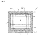
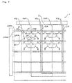
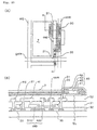
- 1
- display apparatus
- 2
- display section
- 3
- data-side driving circuit
- 4
- scanning-side driving circuit
- 5
- checking circuit
- 6
- pad for mounting
- 7, 7A, 7B
- pixels
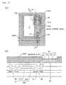
- 10
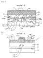
- transparent substrate
- 20
- first TFT
- 21
- gate electrode of first TFT
- 30
- second TFT
- 31
- gate electrode of second TFT
- 40, 40A, 40B
- light-emission elements
- 41
- pixel electrode
- 42
- positive-hole injection layer
- 43
- organic semiconductor film
- 45
- thin lithium-containing aluminum electrode
- 46
- ITO film layer
- 50
- gate insulation film
- 51
- first interlayer insulation film
- 52
- second interlayer insulation film
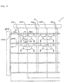
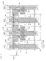
- DA
- dummy wiring layer
- bank
- bank layer
- cap
- holding capacitor
- cline
- capacitance line
- com
- common power-feed line
- gate, gateA, gateB
- scanning lines
- op, opA, opB
- counter electrodes
- sig, sigA, sigB
- data lines
- st, stA, stB
- potential holding electrodes
Claims (13)
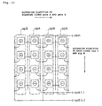
- A display apparatus (1) comprising on a substrate (10): a plurality of scanning lines (gate); a plurality of data lines (sig) extending in a direction intersecting the extension direction of the scanning lines (gate); a plurality of common power-feed lines (com) parallel to the data lines (sig); and pixels (7) formed in a matrix by said data lines (sig) and said scanning lines(gate), each of the pixels (7) comprising: a first thin-film transistor (20) in which a scanning signal is supplied to its gate electrode (21) via said scanning lines(gate); a holding capacitor (cap) for holding an image signal supplied from said data lines (sig) via the first thin-film transistor (20); and a second thin-film transistor (30) in which said image signal held by the holding capacitor (cap) is supplied to its gate electrode (31); and a light-emission element (40) having an organic semiconductor film (43), which emits light by driving current that flows between a pixel electrode (41) and a counter electrode (op) when said pixel electrode (41) is electrically connected to said common power-feed line (com) via said second thin-film transistor (30) in a section between the layers of said pixel electrodes (41) formed for each of said pixels (7) and said counter electrodes (op) opposing the pixel electrodes (41);
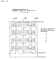
characterised in that pixels (7) to which said driving current is passed through said section between the pixels (7) and the common power-feed line (com) are arranged on both sides of said common power-feed lines (com), and said data lines (sig) pass on a side opposite to said common power-feed lines (com) with respect to the pixels (7). - A display apparatus (1) according to claim 1, wherein, between two pixels (7) arranged in such a manner as to sandwich said common power-feed line (com), said first thin-film transistor (20), said second thin-film transistor (30), and said light-emission elements (40) are disposed in linear symmetry with respect to the common power-feed lines (com).
- A display apparatus (1) according to one of claims 1 and 2, wherein the pitch of the centers of the formation areas of said organic semiconductor films (43) is equal at every interval between adjacent pixels (7) along the extension direction of said scanning lines (gate).
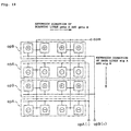
- A display apparatus (1) according to claim 2, wherein the formation area of said organic semiconductor film (43) is surrounded by a bank layer (bank) formed from an insulation film thicker than said organic semiconductor film (43), and the bank layer (bank) is formed in such a manner as to cover said data lines (sig) and said common power-feed lines (com) at the same width dimension.
- A display apparatus (1) according to claim 4, wherein said organic semiconductor film (43) is a film formed within an area surrounded by said bank layer (bank) by an ink-jet method, and said bank layer (bank) is a film for preventing the extrusion of said organic semiconductor film(43) when said organic semiconductor film (43) is formed by the ink-jet method.
- A display apparatus (1) according to one claims 1 to 5, wherein a wiring layer (DA) is formed at a position corresponding to a section between two data lines (sig) passing on a side opposite to said common power-feed lines (com) with respect to said pixels.
- A display apparatus (1) according to claim 6, wherein sampling of an image signal is performed at the same timing in a section between two adjacent data lines (sig) of said plurality of data lines (sig).
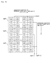
- A display apparatus (1) according to claim 1, wherein two types of pixels (7) in which said light-emission element (40) is driven by a driving current whose polarity is inverted are among a plurality of pixels (7) in which said driving current is passed in a section between the pixels (7) and said same common power-feed line (com).
- A display apparatus (1) according to claim 8, wherein the polarity of the driving current in each pixel (7) is the same in the extension direction of said data lines (sig), and in the extension direction of said scanning lines (gate) the polarity of the driving current in each pixel (7) is inverted for each pixel (7).
- A display apparatus(1) according to claim 8, wherein the polarity of the driving current in each pixel (7) is the same in the extension direction of said data lines (sig), and in the extension direction of said scanning lines (gate) the polarity of driving current in each pixel (7) is inverted every two pixels (7).
- A display apparatus (1) according to claim 8, wherein the polarity of the driving current in each pixel (7) is the same in the extension direction of said scanning lines (gate), and in the extension direction of said data lines (sig) the polarity of the driving current in each pixel is inverted for each pixel (7).
- A display apparatus (1) according to claim 8, wherein the polarity of the driving current in each pixel (7) is the same in the extension direction of said scanning lines (gate), and in the extension direction of said data lines (sig) the polarity of the driving current in each pixel (7) is inverted every two pixels.
- A display apparatus (1) according to claim 8, wherein the polarity of the driving current in each pixel (7) is inverted for each pixel (7) in both the extension direction of said scanning lines (gate) and the extension direction of said data lines (sig).
Priority Applications (4)
| Application Number | Priority Date | Filing Date | Title |
|---|---|---|---|
| EP04078129A EP1505650A3 (en) | 1997-07-02 | 1998-07-01 | Display apparatus |
| EP09166341A EP2112693A3 (en) | 1997-07-02 | 1998-07-01 | Display apparatus |
| EP04078130A EP1505651A3 (en) | 1997-07-02 | 1998-07-01 | Display apparatus |
| EP04078131A EP1505652A3 (en) | 1997-07-02 | 1998-07-01 | Display apparatus |
Applications Claiming Priority (3)
| Application Number | Priority Date | Filing Date | Title |
|---|---|---|---|
| JP17745597 | 1997-07-02 | ||
| JP17745597A JP3520396B2 (en) | 1997-07-02 | 1997-07-02 | Active matrix substrate and display device |
| PCT/JP1998/002982 WO1999001856A1 (en) | 1997-07-02 | 1998-07-01 | Display |
Related Child Applications (3)
| Application Number | Title | Priority Date | Filing Date |
|---|---|---|---|
| EP04078130A Division EP1505651A3 (en) | 1997-07-02 | 1998-07-01 | Display apparatus |
| EP04078131A Division EP1505652A3 (en) | 1997-07-02 | 1998-07-01 | Display apparatus |
| EP04078129A Division EP1505650A3 (en) | 1997-07-02 | 1998-07-01 | Display apparatus |
Publications (3)
| Publication Number | Publication Date |
|---|---|
| EP0935229A1 EP0935229A1 (en) | 1999-08-11 |
| EP0935229A4 EP0935229A4 (en) | 2002-08-21 |
| EP0935229B1 true EP0935229B1 (en) | 2005-03-16 |
Family
ID=16031251
Family Applications (5)
| Application Number | Title | Priority Date | Filing Date |
|---|---|---|---|
| EP98929802A Expired - Lifetime EP0935229B1 (en) | 1997-07-02 | 1998-07-01 | Display |
| EP09166341A Withdrawn EP2112693A3 (en) | 1997-07-02 | 1998-07-01 | Display apparatus |
| EP04078131A Withdrawn EP1505652A3 (en) | 1997-07-02 | 1998-07-01 | Display apparatus |
| EP04078130A Withdrawn EP1505651A3 (en) | 1997-07-02 | 1998-07-01 | Display apparatus |
| EP04078129A Withdrawn EP1505650A3 (en) | 1997-07-02 | 1998-07-01 | Display apparatus |
Family Applications After (4)
| Application Number | Title | Priority Date | Filing Date |
|---|---|---|---|
| EP09166341A Withdrawn EP2112693A3 (en) | 1997-07-02 | 1998-07-01 | Display apparatus |
| EP04078131A Withdrawn EP1505652A3 (en) | 1997-07-02 | 1998-07-01 | Display apparatus |
| EP04078130A Withdrawn EP1505651A3 (en) | 1997-07-02 | 1998-07-01 | Display apparatus |
| EP04078129A Withdrawn EP1505650A3 (en) | 1997-07-02 | 1998-07-01 | Display apparatus |
Country Status (8)
| Country | Link |
|---|---|
| US (7) | US6618029B1 (en) |
| EP (5) | EP0935229B1 (en) |
| JP (1) | JP3520396B2 (en) |
| KR (3) | KR100534218B1 (en) |
| CN (3) | CN1279509C (en) |
| DE (1) | DE69829356T2 (en) |
| TW (1) | TW388854B (en) |
| WO (1) | WO1999001856A1 (en) |
Cited By (5)
| Publication number | Priority date | Publication date | Assignee | Title |
|---|---|---|---|---|
| US8558241B2 (en) | 1999-02-23 | 2013-10-15 | Semiconductor Energy Laboratory Co., Ltd. | Semiconductor device and fabrication method thereof |
| US9123625B2 (en) | 2004-12-06 | 2015-09-01 | Semiconductor Energy Laboratory Co., Ltd. | Display device |
| US9293726B2 (en) | 1999-06-04 | 2016-03-22 | Semiconductor Energy Laboratory Co., Ltd. | Method for manufacturing an electro-optical device |
| US9293483B2 (en) | 1999-04-27 | 2016-03-22 | Semiconductor Energy Laboratory Co. Ltd. | Electronic device and electronic apparatus |
| US9419066B2 (en) | 2000-02-03 | 2016-08-16 | Semiconductor Energy Laboratory Co., Ltd. | Light-emitting device and method of manufacturing the same |
Families Citing this family (203)
| Publication number | Priority date | Publication date | Assignee | Title |
|---|---|---|---|---|
| EP1255240B1 (en) * | 1997-02-17 | 2005-02-16 | Seiko Epson Corporation | Active matrix electroluminescent display with two TFTs and storage capacitor in each pixel |
| US6462722B1 (en) * | 1997-02-17 | 2002-10-08 | Seiko Epson Corporation | Current-driven light-emitting display apparatus and method of producing the same |
| JP3520396B2 (en) * | 1997-07-02 | 2004-04-19 | セイコーエプソン株式会社 | Active matrix substrate and display device |
| JP3580092B2 (en) * | 1997-08-21 | 2004-10-20 | セイコーエプソン株式会社 | Active matrix display |
| WO1999010862A1 (en) * | 1997-08-21 | 1999-03-04 | Seiko Epson Corporation | Active matrix display |
| JP3692844B2 (en) * | 1998-07-24 | 2005-09-07 | セイコーエプソン株式会社 | Electroluminescent device and electronic device |
| US6489952B1 (en) * | 1998-11-17 | 2002-12-03 | Semiconductor Energy Laboratory Co., Ltd. | Active matrix type semiconductor display device |
| TW468269B (en) * | 1999-01-28 | 2001-12-11 | Semiconductor Energy Lab | Serial-to-parallel conversion circuit, and semiconductor display device employing the same |
| JP2000284752A (en) | 1999-01-29 | 2000-10-13 | Seiko Epson Corp | Display device |
| JP2000231346A (en) | 1999-02-09 | 2000-08-22 | Sanyo Electric Co Ltd | Electro-luminescence display device |
| JP4334045B2 (en) * | 1999-02-09 | 2009-09-16 | 三洋電機株式会社 | Electroluminescence display device |
| EP1041641B1 (en) * | 1999-03-26 | 2015-11-04 | Semiconductor Energy Laboratory Co., Ltd. | A method for manufacturing an electrooptical device |
| US6504592B1 (en) * | 1999-06-16 | 2003-01-07 | Nec Corporation | Liquid crystal display and method of manufacturing the same and method of driving the same |
| JP5210473B2 (en) * | 1999-06-21 | 2013-06-12 | 株式会社半導体エネルギー研究所 | Display device |
| JP2001035663A (en) * | 1999-07-27 | 2001-02-09 | Pioneer Electronic Corp | Organic electroluminescence element display device and its manufacture |
| JP2001035662A (en) * | 1999-07-27 | 2001-02-09 | Pioneer Electronic Corp | Organic electroluminescence element display device and its manufacture |
| JP4472073B2 (en) | 1999-09-03 | 2010-06-02 | 株式会社半導体エネルギー研究所 | Display device and manufacturing method thereof |
| JP4530450B2 (en) * | 1999-09-29 | 2010-08-25 | 三洋電機株式会社 | EL display device |
| JP2001100696A (en) | 1999-09-29 | 2001-04-13 | Sanyo Electric Co Ltd | Active matrix type el display device |
| TW535454B (en) * | 1999-10-21 | 2003-06-01 | Semiconductor Energy Lab | Electro-optical device |
| US6587086B1 (en) | 1999-10-26 | 2003-07-01 | Semiconductor Energy Laboratory Co., Ltd. | Electro-optical device |
| US6580094B1 (en) * | 1999-10-29 | 2003-06-17 | Semiconductor Energy Laboratory Co., Ltd. | Electro luminescence display device |
| US6384427B1 (en) * | 1999-10-29 | 2002-05-07 | Semiconductor Energy Laboratory Co., Ltd. | Electronic device |
| JP4596582B2 (en) * | 1999-11-05 | 2010-12-08 | 三洋電機株式会社 | Display device |
| JP2001148291A (en) * | 1999-11-19 | 2001-05-29 | Sony Corp | Display device and its manufacturing method |
| US6750835B2 (en) * | 1999-12-27 | 2004-06-15 | Semiconductor Energy Laboratory Co., Ltd. | Image display device and driving method thereof |
| JP4759719B2 (en) * | 2000-02-01 | 2011-08-31 | モトローラ ソリューションズ インコーポレイテッド | Light emitting device and manufacturing method |
| JP4758163B2 (en) * | 2000-02-03 | 2011-08-24 | 株式会社半導体エネルギー研究所 | Light emitting device |
| TW525305B (en) | 2000-02-22 | 2003-03-21 | Semiconductor Energy Lab | Self-light-emitting device and method of manufacturing the same |
| TW495854B (en) * | 2000-03-06 | 2002-07-21 | Semiconductor Energy Lab | Semiconductor device and manufacturing method thereof |
| TW484238B (en) * | 2000-03-27 | 2002-04-21 | Semiconductor Energy Lab | Light emitting device and a method of manufacturing the same |
| US6847341B2 (en) | 2000-04-19 | 2005-01-25 | Semiconductor Energy Laboratory Co., Ltd. | Electronic device and method of driving the same |
| JP2002033185A (en) * | 2000-05-06 | 2002-01-31 | Semiconductor Energy Lab Co Ltd | Light emitting device and electric apparatus |
| TW554638B (en) * | 2000-05-12 | 2003-09-21 | Semiconductor Energy Lab | Light emitting device |
| US8610645B2 (en) | 2000-05-12 | 2013-12-17 | Semiconductor Energy Laboratory Co., Ltd. | Display device |
| JP4637873B2 (en) * | 2000-05-12 | 2011-02-23 | 株式会社半導体エネルギー研究所 | Display device |
| JP4963145B2 (en) * | 2000-05-18 | 2012-06-27 | 株式会社半導体エネルギー研究所 | Electronic device and electronic equipment |
| TW521256B (en) | 2000-05-18 | 2003-02-21 | Semiconductor Energy Lab | Electronic device and method of driving the same |
| JP4593740B2 (en) * | 2000-07-28 | 2010-12-08 | ルネサスエレクトロニクス株式会社 | Display device |
| US6825820B2 (en) * | 2000-08-10 | 2004-11-30 | Semiconductor Energy Laboratory Co., Ltd. | Display device and electronic device |
| US7430025B2 (en) | 2000-08-23 | 2008-09-30 | Semiconductor Energy Laboratory Co., Ltd. | Portable electronic device |
| US6739931B2 (en) | 2000-09-18 | 2004-05-25 | Semiconductor Energy Laboratory Co., Ltd. | Display device and method of fabricating the display device |
| CN100481159C (en) * | 2000-09-29 | 2009-04-22 | 三洋电机株式会社 | Semiconductor device and display device |
| JP3594126B2 (en) | 2000-10-13 | 2004-11-24 | 日本電気株式会社 | Current drive circuit |
| SG111923A1 (en) * | 2000-12-21 | 2005-06-29 | Semiconductor Energy Lab | Light emitting device and method of manufacturing the same |
| JP2002215063A (en) * | 2001-01-19 | 2002-07-31 | Sony Corp | Active matrix type display device |
| US6717359B2 (en) | 2001-01-29 | 2004-04-06 | Semiconductor Energy Laboratory Co., Ltd. | Light emitting device and manufacturing method thereof |
| JP2002244617A (en) * | 2001-02-15 | 2002-08-30 | Sanyo Electric Co Ltd | Organic el pixel circuit |
| JP3612494B2 (en) | 2001-03-28 | 2005-01-19 | 株式会社日立製作所 | Display device |
| JP3608614B2 (en) | 2001-03-28 | 2005-01-12 | 株式会社日立製作所 | Display device |
| JP3788916B2 (en) * | 2001-03-30 | 2006-06-21 | 株式会社日立製作所 | Light-emitting display device |
| JP2002366057A (en) * | 2001-06-11 | 2002-12-20 | Toshiba Corp | Display device |
| JP3810725B2 (en) | 2001-09-21 | 2006-08-16 | 株式会社半導体エネルギー研究所 | LIGHT EMITTING DEVICE AND ELECTRONIC DEVICE |
| CN101009322B (en) * | 2001-11-09 | 2012-06-27 | 株式会社半导体能源研究所 | Light-emitting device |
| JP4031291B2 (en) * | 2001-11-14 | 2008-01-09 | 東芝松下ディスプレイテクノロジー株式会社 | Liquid crystal display |
| JP3983037B2 (en) * | 2001-11-22 | 2007-09-26 | 株式会社半導体エネルギー研究所 | Light emitting device and manufacturing method thereof |
| JP4050503B2 (en) * | 2001-11-29 | 2008-02-20 | 株式会社日立製作所 | Display device |
| US6949883B2 (en) | 2001-12-06 | 2005-09-27 | Seiko Epson Corporation | Electro-optical device and an electronic apparatus |
| JP3733947B2 (en) * | 2001-12-11 | 2006-01-11 | セイコーエプソン株式会社 | Display device and electronic device |
| CN1245703C (en) | 2001-12-11 | 2006-03-15 | 精工爱普生株式会社 | Display device and electronic machine |
| JP3627739B2 (en) * | 2001-12-11 | 2005-03-09 | セイコーエプソン株式会社 | Display device and electronic device |
| KR100426031B1 (en) * | 2001-12-29 | 2004-04-03 | 엘지.필립스 엘시디 주식회사 | an active matrix organic electroluminescence display and a manufacturing method of the same |
| CN101673508B (en) | 2002-01-18 | 2013-01-09 | 株式会社半导体能源研究所 | Light-emitting device |
| CN100543180C (en) * | 2002-03-08 | 2009-09-23 | 佳能株式会社 | The pattern formation method of organic semiconductor film |
| US7579771B2 (en) | 2002-04-23 | 2009-08-25 | Semiconductor Energy Laboratory Co., Ltd. | Light emitting device and method of manufacturing the same |
| US7786496B2 (en) | 2002-04-24 | 2010-08-31 | Semiconductor Energy Laboratory Co., Ltd. | Semiconductor device and method of manufacturing same |
| JP2003317971A (en) | 2002-04-26 | 2003-11-07 | Semiconductor Energy Lab Co Ltd | Light emitting device and its producing method |
| KR20030086166A (en) * | 2002-05-03 | 2003-11-07 | 엘지.필립스 엘시디 주식회사 | The organic electro-luminescence device and method for fabricating of the same |
| KR100465883B1 (en) * | 2002-05-03 | 2005-01-13 | 엘지.필립스 엘시디 주식회사 | The organic electro-luminescence device and method for fabricating of the same |
| US7897979B2 (en) | 2002-06-07 | 2011-03-01 | Semiconductor Energy Laboratory Co., Ltd. | Light emitting device and manufacturing method thereof |
| JP3977299B2 (en) | 2002-09-18 | 2007-09-19 | セイコーエプソン株式会社 | Electro-optical device, matrix substrate, and electronic apparatus |
| CN101355098A (en) * | 2002-09-25 | 2009-01-28 | 精工爱普生株式会社 | Electro-optical apparatus, matrix substrate, and electronic unit |
| JP3922374B2 (en) | 2002-09-25 | 2007-05-30 | セイコーエプソン株式会社 | Electro-optical device, matrix substrate, and electronic apparatus |
| JP2006113597A (en) * | 2002-09-25 | 2006-04-27 | Seiko Epson Corp | Light emitting apparatus |
| JP2004145011A (en) * | 2002-10-24 | 2004-05-20 | Seiko Epson Corp | Wiring board, circuit board, electro-optic device and method for manufacturing the same, electronic equipment |
| JP2004165067A (en) * | 2002-11-14 | 2004-06-10 | Sanyo Electric Co Ltd | Organic electroluminescent panel |
| JP2004165068A (en) * | 2002-11-14 | 2004-06-10 | Sanyo Electric Co Ltd | Manufacturing method of organic electroluminescent panel |
| JP4042548B2 (en) | 2002-11-29 | 2008-02-06 | セイコーエプソン株式会社 | Electro-optical device and electronic apparatus |
| KR101179155B1 (en) | 2002-12-27 | 2012-09-07 | 가부시키가이샤 한도오따이 에네루기 켄큐쇼 | Display device |
| CN100341154C (en) * | 2003-01-17 | 2007-10-03 | 友达光电股份有限公司 | Organie LED display and its manufacturing method |
| JP2004260133A (en) | 2003-02-04 | 2004-09-16 | Seiko Epson Corp | Wiring board, electro-optical device, manufacturing method thereof and electronic apparatus |
| JP3791616B2 (en) | 2003-02-06 | 2006-06-28 | セイコーエプソン株式会社 | WIRING BOARD, ELECTRO-OPTICAL DEVICE, ITS MANUFACTURING METHOD, AND ELECTRONIC DEVICE |
| JP3791618B2 (en) | 2003-02-20 | 2006-06-28 | セイコーエプソン株式会社 | ELECTRO-OPTICAL DEVICE, MANUFACTURING METHOD THEREOF, AND ELECTRONIC DEVICE |
| JP4134755B2 (en) | 2003-02-28 | 2008-08-20 | ヤマハ株式会社 | Speaker array drive device |
| CN102709478B (en) * | 2003-03-26 | 2016-08-17 | 株式会社半导体能源研究所 | Light-emitting device |
| US7250720B2 (en) * | 2003-04-25 | 2007-07-31 | Semiconductor Energy Laboratory Co., Ltd. | Display device |
| US7557779B2 (en) | 2003-06-13 | 2009-07-07 | Semiconductor Energy Laboratory Co., Ltd. | Display device |
| JP3755521B2 (en) * | 2003-06-13 | 2006-03-15 | セイコーエプソン株式会社 | ORGANIC EL DEVICE AND ITS DRIVE METHOD, LIGHTING DEVICE, AND ELECTRONIC DEVICE |
| JP4590839B2 (en) * | 2003-08-01 | 2010-12-01 | ソニー株式会社 | Semiconductor substrate, liquid crystal display device and projector |
| KR100886292B1 (en) | 2003-09-09 | 2009-03-04 | 산요덴키가부시키가이샤 | Semiconductor module and semiconductor device including circuit components, manufacturing method and display device thereof |
| KR100560787B1 (en) | 2003-11-05 | 2006-03-13 | 삼성에스디아이 주식회사 | Electro luminescene display pannel |
| US20060139342A1 (en) * | 2004-12-29 | 2006-06-29 | Gang Yu | Electronic devices and processes for forming electronic devices |
| KR100686343B1 (en) * | 2003-11-29 | 2007-02-22 | 삼성에스디아이 주식회사 | Organic electro luminescence display |
| KR100963403B1 (en) * | 2003-12-08 | 2010-06-14 | 엘지디스플레이 주식회사 | Liquid Crystal Display Device and Driving Method Thereof |
| JP2005338592A (en) * | 2004-05-28 | 2005-12-08 | Sony Corp | Display device |
| US8378930B2 (en) | 2004-05-28 | 2013-02-19 | Sony Corporation | Pixel circuit and display device having symmetric pixel circuits and shared voltage lines |
| KR100583126B1 (en) * | 2004-06-25 | 2006-05-23 | 삼성에스디아이 주식회사 | Light emitting display |
| KR100637164B1 (en) * | 2004-06-26 | 2006-10-20 | 삼성에스디아이 주식회사 | Active matrix type electroluminescence display device |
| TWI467541B (en) | 2004-09-16 | 2015-01-01 | Semiconductor Energy Lab | Display device and driving method of the same |
| JP5122818B2 (en) * | 2004-09-17 | 2013-01-16 | シャープ株式会社 | Method for manufacturing thin film semiconductor device |
| US7105855B2 (en) * | 2004-09-20 | 2006-09-12 | Eastman Kodak Company | Providing driving current arrangement for OLED device |
| JP4379278B2 (en) * | 2004-09-21 | 2009-12-09 | カシオ計算機株式会社 | Transistor array substrate and display panel |
| JP2006098641A (en) * | 2004-09-29 | 2006-04-13 | Seiko Epson Corp | Thin-film semiconductor device, electro-optical device, and electronic equipment |
| US7753751B2 (en) | 2004-09-29 | 2010-07-13 | Semiconductor Energy Laboratory Co., Ltd. | Method of fabricating the display device |
| JP4063266B2 (en) * | 2004-09-30 | 2008-03-19 | セイコーエプソン株式会社 | Thin film semiconductor device manufacturing method, thin film semiconductor device, electro-optical device, and electronic apparatus |
| KR20060065333A (en) * | 2004-12-10 | 2006-06-14 | 삼성전자주식회사 | Display panel and display device including sensing element |
| US20060138403A1 (en) * | 2004-12-29 | 2006-06-29 | Gang Yu | Organic electronic devices including pixels |
| US7612368B2 (en) * | 2004-12-29 | 2009-11-03 | E.I. Du Pont De Nemours And Company | Organic bottom emission electronic device |
| KR20060077870A (en) * | 2004-12-31 | 2006-07-05 | 엘지.필립스 엘시디 주식회사 | In-plain switching liquid crystal display device |
| US7462897B2 (en) | 2005-01-31 | 2008-12-09 | Semiconductor Energy Laboratory Co., Ltd. | Light emitting device and electronic device |
| KR101100885B1 (en) * | 2005-01-31 | 2012-01-02 | 삼성전자주식회사 | Thin film transistor array panel for organic electro-luminescence |
| JP2006251453A (en) * | 2005-03-11 | 2006-09-21 | Sanyo Electric Co Ltd | Active matrix type display device and method for driving the same |
| US8681077B2 (en) * | 2005-03-18 | 2014-03-25 | Semiconductor Energy Laboratory Co., Ltd. | Semiconductor device, and display device, driving method and electronic apparatus thereof |
| US7208388B2 (en) * | 2005-04-08 | 2007-04-24 | Texas Instruments Incorporated | Thin film resistor head structure and method for reducing head resistivity variance |
| US8253179B2 (en) * | 2005-05-13 | 2012-08-28 | Semiconductor Energy Laboratory Co., Ltd. | Semiconductor device and manufacturing method of the same |
| KR101169053B1 (en) * | 2005-06-30 | 2012-07-26 | 엘지디스플레이 주식회사 | Organic Light Emitting Diode Display |
| JP2007103584A (en) | 2005-10-03 | 2007-04-19 | Ricoh Co Ltd | Transistor element, display device and manufacturing methods thereof |
| TWI460851B (en) | 2005-10-17 | 2014-11-11 | Semiconductor Energy Lab | Semiconductor device and manufacturing method thereof |
| US20070090385A1 (en) * | 2005-10-21 | 2007-04-26 | Semiconductor Energy Laboratory Co., Ltd. | Semiconductor device |
| KR101256665B1 (en) * | 2005-12-30 | 2013-04-19 | 엘지디스플레이 주식회사 | Liquid crystal panel |
| KR101240654B1 (en) * | 2006-05-09 | 2013-03-08 | 삼성디스플레이 주식회사 | Thin film transistor array panel and method for manufacturing the same |
| JP2007317384A (en) * | 2006-05-23 | 2007-12-06 | Canon Inc | Organic electroluminescence display device, its manufacturing method, repair method and repair unit |
| JP4957090B2 (en) * | 2006-06-22 | 2012-06-20 | ソニー株式会社 | Display device and video display device |
| KR101244898B1 (en) * | 2006-06-28 | 2013-03-19 | 삼성디스플레이 주식회사 | Organic Thin Film Transistor Substrate And Fabricating Method Thereof |
| US7467431B2 (en) * | 2006-11-01 | 2008-12-23 | Weedling Robert E | Patient incline device having centerline spinal support |
| CN1963906B (en) * | 2006-11-10 | 2010-05-12 | 北京巨数数字技术开发有限公司 | Driving control system for overturn row-by-row and its method and LED display screen |
| US8184797B1 (en) * | 2007-05-18 | 2012-05-22 | Richard Rosen | System and method for improved directory assistance searches |
| KR101103615B1 (en) | 2007-07-30 | 2012-01-09 | 쿄세라 코포레이션 | Image display device |
| JP5251034B2 (en) * | 2007-08-15 | 2013-07-31 | ソニー株式会社 | Display device and electronic device |
| KR20090035228A (en) * | 2007-10-05 | 2009-04-09 | 주식회사 동진쎄미켐 | Display device driven by electric filed |
| JP2009122652A (en) * | 2007-10-23 | 2009-06-04 | Sony Corp | Display device and electronic apparatus |
| CN101796619B (en) * | 2007-11-02 | 2013-03-06 | 夏普株式会社 | Circuit board and display device |
| JP4606450B2 (en) * | 2007-11-05 | 2011-01-05 | 株式会社日立製作所 | Display device |
| KR100870653B1 (en) * | 2007-11-27 | 2008-11-26 | 엘지전자 주식회사 | Organic light emitting device |
| JP4737221B2 (en) * | 2008-04-16 | 2011-07-27 | ソニー株式会社 | Display device |
| JP2009288773A (en) * | 2008-04-30 | 2009-12-10 | Sony Corp | Display device |
| JP4582195B2 (en) * | 2008-05-29 | 2010-11-17 | ソニー株式会社 | Display device |
| JP2010008654A (en) * | 2008-06-26 | 2010-01-14 | Kyocera Corp | Organic el image display |
| US8021935B2 (en) * | 2008-10-01 | 2011-09-20 | Hewlett-Packard Development Company, L.P. | Thin film device fabrication process using 3D template |
| JP2010062003A (en) * | 2008-09-04 | 2010-03-18 | Hitachi Displays Ltd | Display device |
| JP5309879B2 (en) * | 2008-10-17 | 2013-10-09 | ソニー株式会社 | panel |
| KR101540341B1 (en) * | 2008-10-17 | 2015-07-30 | 삼성전자주식회사 | Panel structure, display device comprising the panel structure and manufacturing methods thereof |
| KR101268963B1 (en) * | 2008-10-30 | 2013-05-30 | 엘지디스플레이 주식회사 | Liquid Crystal Display |
| JP2010122355A (en) * | 2008-11-18 | 2010-06-03 | Canon Inc | Display apparatus and camera |
| JP5623107B2 (en) * | 2009-04-22 | 2014-11-12 | キヤノン株式会社 | Semiconductor device |
| KR101073174B1 (en) * | 2009-07-31 | 2011-10-12 | 삼성모바일디스플레이주식회사 | Pixel and Organic Light Emitting Display Device Having the Same |
| KR101835748B1 (en) | 2009-10-09 | 2018-03-07 | 가부시키가이샤 한도오따이 에네루기 켄큐쇼 | Light-emitting display device and electronic device including the same |
| JP5312294B2 (en) * | 2009-10-30 | 2013-10-09 | キヤノン株式会社 | Light emitting apparatus and exposure apparatus |
| KR101754799B1 (en) * | 2010-03-26 | 2017-07-07 | 삼성전자주식회사 | Pixel circuit of display panel, display apparatus comprising the same, and controlling method of the display apparatus |
| KR101223722B1 (en) * | 2010-04-02 | 2013-01-17 | 삼성디스플레이 주식회사 | Organic light emitting display device |
| JP5482393B2 (en) | 2010-04-08 | 2014-05-07 | ソニー株式会社 | Display device, display device layout method, and electronic apparatus |
| JP5455126B2 (en) | 2010-04-28 | 2014-03-26 | 株式会社ジャパンディスプレイ | Display device with touch detection function, driving method, and electronic device |
| KR101749265B1 (en) * | 2010-04-30 | 2017-06-21 | 삼성디스플레이 주식회사 | Array substrate and fabricating method for the same |
| JP2012047807A (en) * | 2010-08-24 | 2012-03-08 | Sony Corp | Display device and electronic equipment |
| KR101768848B1 (en) * | 2010-10-28 | 2017-08-18 | 삼성디스플레이 주식회사 | Organic electroluminescence emitting display device |
| TWI445170B (en) * | 2010-12-03 | 2014-07-11 | Au Optronics Corp | Organic light emitting diode pixel array |
| JP5682385B2 (en) | 2011-03-10 | 2015-03-11 | セイコーエプソン株式会社 | Electro-optical device and electronic apparatus |
| TWI463583B (en) * | 2011-08-10 | 2014-12-01 | Chunghwa Picture Tubes Ltd | Display apparatus |
| JP5793058B2 (en) * | 2011-10-28 | 2015-10-14 | 株式会社Joled | Display panel, display device and electronic device |
| JP5939076B2 (en) * | 2012-07-31 | 2016-06-22 | ソニー株式会社 | Display device, driving circuit, driving method, and electronic apparatus |
| JP6302186B2 (en) | 2012-08-01 | 2018-03-28 | 株式会社半導体エネルギー研究所 | Display device |
| KR101434366B1 (en) | 2012-08-24 | 2014-08-26 | 삼성디스플레이 주식회사 | Thin-film transistor array substrate, display apparatus comprising the same |
| JP6076683B2 (en) | 2012-10-17 | 2017-02-08 | 株式会社半導体エネルギー研究所 | Light emitting device |
| JP6204012B2 (en) | 2012-10-17 | 2017-09-27 | 株式会社半導体エネルギー研究所 | Light emitting device |
| JP6155020B2 (en) | 2012-12-21 | 2017-06-28 | 株式会社半導体エネルギー研究所 | Light emitting device and manufacturing method thereof |
| JP6216125B2 (en) | 2013-02-12 | 2017-10-18 | 株式会社半導体エネルギー研究所 | Light emitting device |
| JP6104649B2 (en) | 2013-03-08 | 2017-03-29 | 株式会社半導体エネルギー研究所 | Light emitting device |
| JP6182985B2 (en) * | 2013-06-05 | 2017-08-23 | セイコーエプソン株式会社 | Electro-optical device, method of manufacturing electro-optical device, and electronic apparatus |
| JP6225511B2 (en) | 2013-07-02 | 2017-11-08 | セイコーエプソン株式会社 | Display device and electronic device |
| CN103413519B (en) * | 2013-07-18 | 2016-05-11 | 京东方科技集团股份有限公司 | A kind of image element circuit and driving method, array base palte and display unit |
| JP6164059B2 (en) | 2013-11-15 | 2017-07-19 | ソニー株式会社 | Display device, electronic apparatus, and display device driving method |
| KR102066139B1 (en) | 2013-11-21 | 2020-01-14 | 엘지디스플레이 주식회사 | Organic light emitting display panel and organic light emitting display device including the same |
| JP5651763B2 (en) * | 2013-11-28 | 2015-01-14 | 株式会社半導体エネルギー研究所 | Display device |
| KR20150105523A (en) * | 2014-03-06 | 2015-09-17 | 삼성디스플레이 주식회사 | Liquid crystal display apparatus |
| CN103972243B (en) * | 2014-04-24 | 2017-03-29 | 京东方科技集团股份有限公司 | A kind of array base palte and preparation method thereof, display device |
| CN104078003B (en) * | 2014-06-18 | 2016-08-31 | 京东方科技集团股份有限公司 | Image element circuit and display device |
| KR102471668B1 (en) * | 2014-11-10 | 2022-11-29 | 엘지디스플레이 주식회사 | Organic Light Emitting Diode Display And Method For Manufacturing The Same |
| KR102490881B1 (en) * | 2014-12-26 | 2023-01-25 | 삼성디스플레이 주식회사 | Organic light emitting display device and manufacturing method of the same |
| JP5947963B2 (en) * | 2015-07-24 | 2016-07-06 | 株式会社半導体エネルギー研究所 | Display device and method for manufacturing display device |
| KR102555404B1 (en) * | 2015-08-06 | 2023-07-13 | 엘지디스플레이 주식회사 | Flexible Display and Method for Manufacturing the Same |
| TWI624094B (en) * | 2015-11-30 | 2018-05-11 | Lg顯示器股份有限公司 | Organic emitting diode and organic light emitting diode display device including the same |
| CN107204352B (en) * | 2016-03-16 | 2020-06-16 | 昆山工研院新型平板显示技术中心有限公司 | OLED display panel and manufacturing method thereof |
| TWI576799B (en) | 2016-03-22 | 2017-04-01 | 友達光電股份有限公司 | Display panel |
| US10510820B2 (en) | 2016-09-09 | 2019-12-17 | Sony Semiconductor Solutions Corporation | Display device and electronic apparatus |
| KR102613863B1 (en) | 2016-09-22 | 2023-12-18 | 삼성디스플레이 주식회사 | Display device |
| KR102611958B1 (en) | 2016-09-23 | 2023-12-12 | 삼성디스플레이 주식회사 | Display device |
| KR20180061568A (en) * | 2016-11-29 | 2018-06-08 | 삼성디스플레이 주식회사 | Display device |
| KR102559096B1 (en) | 2016-11-29 | 2023-07-26 | 삼성디스플레이 주식회사 | Display device |
| KR20180077439A (en) | 2016-12-29 | 2018-07-09 | 엘지디스플레이 주식회사 | Electroluminescent display device and method of manufacturing the same |
| CN108333843B (en) * | 2017-01-20 | 2020-11-13 | 京东方科技集团股份有限公司 | Double-grid line array substrate and display device |
| KR20180093188A (en) * | 2017-02-10 | 2018-08-21 | 삼성디스플레이 주식회사 | Organic light emitting display device |
| KR20180096875A (en) | 2017-02-21 | 2018-08-30 | 삼성디스플레이 주식회사 | Display device |
| CN107342037B (en) * | 2017-09-01 | 2020-12-08 | 京东方科技集团股份有限公司 | Data conversion method, device and computer readable storage medium |
| JP6436209B2 (en) * | 2017-10-05 | 2018-12-12 | セイコーエプソン株式会社 | Display device and electronic device |
| CN107731163B (en) | 2017-10-30 | 2019-10-18 | 合肥鑫晟光电科技有限公司 | Pixel-driving circuit and its driving method, display device |
| KR102612371B1 (en) * | 2017-12-05 | 2023-12-08 | 엘지디스플레이 주식회사 | Display Device |
| KR102566157B1 (en) * | 2018-06-28 | 2023-08-11 | 삼성디스플레이 주식회사 | Display device |
| CN108986747B (en) * | 2018-07-25 | 2020-07-28 | 京东方科技集团股份有限公司 | Array substrate, organic electroluminescent display panel and display device |
| CN110265408B (en) * | 2019-06-19 | 2021-10-29 | 京东方科技集团股份有限公司 | Array substrate, display panel and display device |
| KR20210021769A (en) | 2019-08-19 | 2021-03-02 | 삼성전자주식회사 | Display device |
| WO2021230883A1 (en) * | 2020-05-15 | 2021-11-18 | Hewlett-Packard Development Company, L.P. | Controllers to drive display lines |
| WO2023136300A1 (en) * | 2022-01-17 | 2023-07-20 | 京セラ株式会社 | Light-emitting device and display device |
| CN115331619B (en) * | 2022-10-12 | 2023-01-31 | 惠科股份有限公司 | Pixel driving circuit, display panel and display device |
Family Cites Families (107)
| Publication number | Priority date | Publication date | Assignee | Title |
|---|---|---|---|---|
| US4042854A (en) * | 1975-11-21 | 1977-08-16 | Westinghouse Electric Corporation | Flat panel display device with integral thin film transistor control system |
| US4006383A (en) * | 1975-11-28 | 1977-02-01 | Westinghouse Electric Corporation | Electroluminescent display panel with enlarged active display areas |
| US4087792A (en) * | 1977-03-03 | 1978-05-02 | Westinghouse Electric Corp. | Electro-optic display system |
| JPS617479A (en) | 1978-01-30 | 1986-01-14 | テキサス インスツルメンツ インコ−ポレイテツド | Method of inspecting integrated circuit |
| JPS5958468A (en) | 1982-09-29 | 1984-04-04 | 富士通株式会社 | Display |
| US4636038A (en) * | 1983-07-09 | 1987-01-13 | Canon Kabushiki Kaisha | Electric circuit member and liquid crystal display device using said member |
| JPH0762743B2 (en) | 1983-07-09 | 1995-07-05 | キヤノン株式会社 | Liquid crystal device |
| FR2629634B1 (en) * | 1984-12-18 | 1990-10-12 | Thomson Csf | PROGRESSIVE WAVE TUBE HAVING A PROPELLER-TYPE DELAY LINE FIXED TO A SLEEVE THROUGH BORON NITRIDE DIELECTRIC SUPPORT |
| US4738514A (en) * | 1986-01-16 | 1988-04-19 | Rca Corporation | Crystal variation compensation circuit for liquid crystal displays |
| US4820222A (en) * | 1986-12-31 | 1989-04-11 | Alphasil, Inc. | Method of manufacturing flat panel backplanes including improved testing and yields thereof and displays made thereby |
| JPH01186655A (en) | 1988-01-14 | 1989-07-26 | Fujitsu Ltd | Semiconductor integrated circuit |
| JPH088146B2 (en) | 1988-08-31 | 1996-01-29 | 松下電器産業株式会社 | Color EL display device and manufacturing method thereof |
| US5892244A (en) * | 1989-01-10 | 1999-04-06 | Mitsubishi Denki Kabushiki Kaisha | Field effect transistor including πconjugate polymer and liquid crystal display including the field effect transistor |
| AU638288B2 (en) * | 1989-10-18 | 1993-06-24 | Noritake Co., Limited | Plasma display panel and method of manufacturing the same |
| JP3112021B2 (en) * | 1990-07-09 | 2000-11-27 | 株式会社日立製作所 | Semiconductor memory |
| JPH0470820A (en) * | 1990-07-12 | 1992-03-05 | Matsushita Electric Ind Co Ltd | Active matrix type flat plate display device |
| DE9012949U1 (en) * | 1990-09-11 | 1991-01-03 | Siemens Ag, 8000 Muenchen, De | |
| US5123876A (en) * | 1990-10-30 | 1992-06-23 | Mccullough Fredrick L | Attic fan cover |
| US5256562A (en) * | 1990-12-31 | 1993-10-26 | Kopin Corporation | Method for manufacturing a semiconductor device using a circuit transfer film |
| US5177406A (en) * | 1991-04-29 | 1993-01-05 | General Motors Corporation | Active matrix vacuum fluorescent display with compensation for variable phosphor efficiency |
| US5631753A (en) * | 1991-06-28 | 1997-05-20 | Dai Nippon Printing Co., Ltd. | Black matrix base board and manufacturing method therefor, and liquid crystal display panel and manufacturing method therefor |
| US5317432A (en) * | 1991-09-04 | 1994-05-31 | Sony Corporation | Liquid crystal display device with a capacitor and a thin film transistor in a trench for each pixel |
| JP2784615B2 (en) * | 1991-10-16 | 1998-08-06 | 株式会社半導体エネルギー研究所 | Electro-optical display device and driving method thereof |
| WO1993011455A1 (en) * | 1991-11-29 | 1993-06-10 | Seiko Epson Corporation | Liquid crystal display and method of manufacturing same |
| US5302966A (en) * | 1992-06-02 | 1994-04-12 | David Sarnoff Research Center, Inc. | Active matrix electroluminescent display and method of operation |
| US5627557A (en) * | 1992-08-20 | 1997-05-06 | Sharp Kabushiki Kaisha | Display apparatus |
| DE4240427C1 (en) * | 1992-12-02 | 1994-01-20 | Novopress Gmbh | Press tool |
| US5592199A (en) * | 1993-01-27 | 1997-01-07 | Sharp Kabushiki Kaisha | Assembly structure of a flat type device including a panel having electrode terminals disposed on a peripheral portion thereof and method for assembling the same |
| US5506375A (en) * | 1993-02-22 | 1996-04-09 | Wacom Co., Ltd. | Circuit board for coordinate detecting apparatus with noise suppression |
| JP3244843B2 (en) * | 1993-03-08 | 2002-01-07 | 株式会社日立製作所 | Color cathode ray tube |
| JP2812851B2 (en) * | 1993-03-24 | 1998-10-22 | シャープ株式会社 | Reflective liquid crystal display |
| JPH06325869A (en) * | 1993-05-18 | 1994-11-25 | Mitsubishi Kasei Corp | Organic electroluminescent panel |
| US5416034A (en) * | 1993-06-30 | 1995-05-16 | Sgs-Thomson Microelectronics, Inc. | Method of making resistor with silicon-rich silicide contacts for an integrated circuit |
| JPH0757871A (en) | 1993-08-19 | 1995-03-03 | Hitachi Ltd | Electroluminescence display device |
| EP0644523B1 (en) * | 1993-08-30 | 1999-01-13 | Sharp Kabushiki Kaisha | Data signal line structure in an active matrix liquid crystal display |
| US5485293A (en) * | 1993-09-29 | 1996-01-16 | Honeywell Inc. | Liquid crystal display including color triads with split pixels |
| JP2821347B2 (en) * | 1993-10-12 | 1998-11-05 | 日本電気株式会社 | Current control type light emitting element array |
| JPH07153576A (en) | 1993-11-30 | 1995-06-16 | Mitsubishi Chem Corp | Organic electroluminescent panel |
| JPH07181927A (en) | 1993-12-24 | 1995-07-21 | Sharp Corp | Image display device |
| TW277129B (en) * | 1993-12-24 | 1996-06-01 | Sharp Kk | |
| JP3463362B2 (en) | 1993-12-28 | 2003-11-05 | カシオ計算機株式会社 | Method of manufacturing electroluminescent device and electroluminescent device |
| US5701055A (en) * | 1994-03-13 | 1997-12-23 | Pioneer Electronic Corporation | Organic electoluminescent display panel and method for manufacturing the same |
| US5432358A (en) * | 1994-03-24 | 1995-07-11 | Motorola, Inc. | Integrated electro-optical package |
| JPH07283378A (en) | 1994-04-08 | 1995-10-27 | Sony Corp | Wiring structure of gate array |
| EP0686958B1 (en) * | 1994-06-06 | 2003-10-29 | Canon Kabushiki Kaisha | DC compensation for interlaced display |
| KR100360356B1 (en) * | 1994-06-24 | 2003-02-17 | 가부시끼가이샤 히다치 세이사꾸쇼 | Active Matrix Liquid Crystal Display |
| JPH0855910A (en) * | 1994-07-29 | 1996-02-27 | Texas Instr Inc <Ti> | Manufacture of semiconductor device |
| US5525867A (en) * | 1994-08-05 | 1996-06-11 | Hughes Aircraft Company | Electroluminescent display with integrated drive circuitry |
| US5587329A (en) * | 1994-08-24 | 1996-12-24 | David Sarnoff Research Center, Inc. | Method for fabricating a switching transistor having a capacitive network proximate a drift region |
| DE69535970D1 (en) | 1994-12-14 | 2009-08-06 | Eastman Kodak Co | Electroluminescent device with an organic electroluminescent layer |
| US5684365A (en) * | 1994-12-14 | 1997-11-04 | Eastman Kodak Company | TFT-el display panel using organic electroluminescent media |
| US5550066A (en) * | 1994-12-14 | 1996-08-27 | Eastman Kodak Company | Method of fabricating a TFT-EL pixel |
| US6115014A (en) * | 1994-12-26 | 2000-09-05 | Casio Computer Co., Ltd. | Liquid crystal display by means of time-division color mixing and voltage driving methods using birefringence |
| KR0145902B1 (en) * | 1995-01-27 | 1998-09-15 | 김광호 | Resistance part and its manufacturing method of thin film transistor liquid crystal display elements |
| US5804917A (en) * | 1995-01-31 | 1998-09-08 | Futaba Denshi Kogyo K.K. | Organic electroluminescent display device and method for manufacturing same |
| JP3208638B2 (en) | 1995-01-31 | 2001-09-17 | 双葉電子工業株式会社 | Organic electroluminescent display device and method of manufacturing the same |
| DE69623443T2 (en) * | 1995-02-06 | 2003-01-23 | Idemitsu Kosan Co | VARIOUS COLORED LIGHT EMISSION DEVICE AND METHOD FOR PRODUCING THE SAME |
| JP3401356B2 (en) * | 1995-02-21 | 2003-04-28 | パイオニア株式会社 | Organic electroluminescent display panel and method of manufacturing the same |
| US5726678A (en) * | 1995-03-06 | 1998-03-10 | Thomson Consumer Electronics, S.A. | Signal disturbance reduction arrangement for a liquid crystal display |
| US5640067A (en) * | 1995-03-24 | 1997-06-17 | Tdk Corporation | Thin film transistor, organic electroluminescence display device and manufacturing method of the same |
| DE69622618T2 (en) * | 1995-04-04 | 2003-03-20 | Canon Kk | Metal-containing composition for forming an electron-emitting device and method of manufacturing an electron-emitting device, an electron source, and an image forming apparatus |
| US5641974A (en) * | 1995-06-06 | 1997-06-24 | Ois Optical Imaging Systems, Inc. | LCD with bus lines overlapped by pixel electrodes and photo-imageable insulating layer therebetween |
| JP3286152B2 (en) * | 1995-06-29 | 2002-05-27 | シャープ株式会社 | Thin film transistor circuit and image display device |
| JP3107743B2 (en) * | 1995-07-31 | 2000-11-13 | カシオ計算機株式会社 | Electron-emitting electrode, method of manufacturing the same, and cold cathode fluorescent tube and plasma display using the same |
| JPH0981053A (en) | 1995-09-07 | 1997-03-28 | Casio Comput Co Ltd | Electric field light emitting element and its driving method |
| JPH0980416A (en) * | 1995-09-13 | 1997-03-28 | Sharp Corp | Liquid crystal display device |
| JPH0982476A (en) | 1995-09-14 | 1997-03-28 | Casio Comput Co Ltd | Organic electroluminescent element |
| US5675185A (en) * | 1995-09-29 | 1997-10-07 | International Business Machines Corporation | Semiconductor structure incorporating thin film transistors with undoped cap oxide layers |
| JPH09105953A (en) * | 1995-10-12 | 1997-04-22 | Semiconductor Energy Lab Co Ltd | Liquid crystal display device |
| JP3526992B2 (en) * | 1995-11-06 | 2004-05-17 | 株式会社半導体エネルギー研究所 | Matrix type display device |
| JPH09230311A (en) * | 1995-11-14 | 1997-09-05 | Semiconductor Energy Lab Co Ltd | Display device |
| TW329500B (en) * | 1995-11-14 | 1998-04-11 | Handotai Energy Kenkyusho Kk | Electro-optical device |
| US6002463A (en) * | 1996-01-30 | 1999-12-14 | Seiko Epson Corporation | Liquid crystal device having a light blocking layer provided over an alignment layer, method for making the same |
| US6175186B1 (en) * | 1996-02-26 | 2001-01-16 | Idemitsu Kosan Co., Ltd. | Organic electroluminescent element and method for manufacturing the same |
| TW374860B (en) * | 1996-04-30 | 1999-11-21 | Matsushita Electric Ind Co Ltd | Active matrix liquid crystal display for projection |
| KR100479000B1 (en) * | 1996-05-15 | 2005-08-01 | 세이코 엡슨 가부시키가이샤 | Manufacturing method of thin film device, liquid crystal panel and electronic device and thin film device |
| JP2853656B2 (en) * | 1996-05-22 | 1999-02-03 | 日本電気株式会社 | LCD panel |
| JP3640224B2 (en) * | 1996-06-25 | 2005-04-20 | 株式会社半導体エネルギー研究所 | LCD panel |
| AU4644097A (en) | 1996-07-09 | 1998-02-10 | James A. Patterson | Nuclear transmuted elements having unnatural isotopic distributions by electrolysis and method of production |
| US5812188A (en) * | 1996-07-12 | 1998-09-22 | Adair; Edwin L. | Sterile encapsulated endoscopic video monitor |
| CN1173315C (en) | 1996-09-19 | 2004-10-27 | 精工爱普生株式会社 | Matrix type indicator element and method of production thereof |
| JP3992797B2 (en) * | 1996-09-25 | 2007-10-17 | 東芝松下ディスプレイテクノロジー株式会社 | Liquid crystal display |
| EP1465257A1 (en) * | 1996-09-26 | 2004-10-06 | Seiko Epson Corporation | Display apparatus |
| US6011531A (en) | 1996-10-21 | 2000-01-04 | Xerox Corporation | Methods and applications of combining pixels to the gate and data lines for 2-D imaging and display arrays |
| GB9623185D0 (en) * | 1996-11-09 | 1997-01-08 | Epigem Limited | Improved micro relief element and preparation thereof |
| JP3899566B2 (en) | 1996-11-25 | 2007-03-28 | セイコーエプソン株式会社 | Manufacturing method of organic EL display device |
| DE69739633D1 (en) | 1996-11-28 | 2009-12-10 | Casio Computer Co Ltd | display device |
| JP3392672B2 (en) * | 1996-11-29 | 2003-03-31 | 三洋電機株式会社 | Display device |
| US6462722B1 (en) * | 1997-02-17 | 2002-10-08 | Seiko Epson Corporation | Current-driven light-emitting display apparatus and method of producing the same |
| EP1255240B1 (en) * | 1997-02-17 | 2005-02-16 | Seiko Epson Corporation | Active matrix electroluminescent display with two TFTs and storage capacitor in each pixel |
| JP3641342B2 (en) * | 1997-03-07 | 2005-04-20 | Tdk株式会社 | Semiconductor device and organic EL display device |
| US5903246A (en) * | 1997-04-04 | 1999-05-11 | Sarnoff Corporation | Circuit and method for driving an organic light emitting diode (O-LED) display |
| JPH113048A (en) | 1997-06-10 | 1999-01-06 | Canon Inc | Electroluminescent element and device and their production |
| JP3541625B2 (en) * | 1997-07-02 | 2004-07-14 | セイコーエプソン株式会社 | Display device and active matrix substrate |
| JP3520396B2 (en) * | 1997-07-02 | 2004-04-19 | セイコーエプソン株式会社 | Active matrix substrate and display device |
| JPH1154268A (en) * | 1997-08-08 | 1999-02-26 | Sanyo Electric Co Ltd | Organic electroluminescent display device |
| JP3580092B2 (en) | 1997-08-21 | 2004-10-20 | セイコーエプソン株式会社 | Active matrix display |
| JP3804646B2 (en) | 1997-08-21 | 2006-08-02 | セイコーエプソン株式会社 | Display device |
| WO1999010862A1 (en) * | 1997-08-21 | 1999-03-04 | Seiko Epson Corporation | Active matrix display |
| JP3830238B2 (en) * | 1997-08-29 | 2006-10-04 | セイコーエプソン株式会社 | Active matrix type device |
| US6229508B1 (en) * | 1997-09-29 | 2001-05-08 | Sarnoff Corporation | Active matrix light emitting diode pixel structure and concomitant method |
| JP3543170B2 (en) * | 1998-02-24 | 2004-07-14 | カシオ計算機株式会社 | Electroluminescent device and method of manufacturing the same |
| JP3203227B2 (en) * | 1998-02-27 | 2001-08-27 | 三洋電機株式会社 | Display device manufacturing method |
| TW410478B (en) * | 1998-05-29 | 2000-11-01 | Lucent Technologies Inc | Thin-film transistor monolithically integrated with an organic light-emitting diode |
| US6561023B2 (en) * | 2001-04-23 | 2003-05-13 | The United States Of America As Represented By The Secretary Of The Navy | Cellulose-based water sensing actuator |
| KR100423395B1 (en) * | 2001-07-02 | 2004-03-18 | 삼성전기주식회사 | A Chip Antenna |
| JP3705264B2 (en) * | 2001-12-18 | 2005-10-12 | セイコーエプソン株式会社 | Display device and electronic device |
-
1997
- 1997-07-02 JP JP17745597A patent/JP3520396B2/en not_active Expired - Lifetime
-
1998
- 1998-07-01 EP EP98929802A patent/EP0935229B1/en not_active Expired - Lifetime
- 1998-07-01 KR KR10-1999-7001473A patent/KR100534218B1/en not_active IP Right Cessation
- 1998-07-01 CN CNB031367534A patent/CN1279509C/en not_active Expired - Lifetime
- 1998-07-01 EP EP09166341A patent/EP2112693A3/en not_active Withdrawn
- 1998-07-01 CN CNB031367526A patent/CN1279508C/en not_active Expired - Lifetime
- 1998-07-01 US US09/242,904 patent/US6618029B1/en not_active Expired - Lifetime
- 1998-07-01 KR KR10-2005-7010943A patent/KR100525259B1/en not_active IP Right Cessation
- 1998-07-01 EP EP04078131A patent/EP1505652A3/en not_active Withdrawn
- 1998-07-01 WO PCT/JP1998/002982 patent/WO1999001856A1/en active IP Right Grant
- 1998-07-01 KR KR1020057010946A patent/KR100572239B1/en not_active IP Right Cessation
- 1998-07-01 CN CN98800923A patent/CN1129103C/en not_active Expired - Lifetime
- 1998-07-01 EP EP04078130A patent/EP1505651A3/en not_active Withdrawn
- 1998-07-01 EP EP04078129A patent/EP1505650A3/en not_active Withdrawn
- 1998-07-01 DE DE69829356T patent/DE69829356T2/en not_active Expired - Lifetime
- 1998-07-01 TW TW087110665A patent/TW388854B/en not_active IP Right Cessation
-
2003
- 2003-02-19 US US10/367,849 patent/US8803773B2/en not_active Expired - Fee Related
- 2003-06-10 US US10/457,446 patent/US7460094B2/en not_active Expired - Lifetime
-
2004
- 2004-10-21 US US10/968,984 patent/US7397451B2/en not_active Expired - Lifetime
-
2008
- 2008-03-03 US US12/073,258 patent/US8310476B2/en not_active Expired - Lifetime
- 2008-03-04 US US12/073,341 patent/US8334858B2/en not_active Expired - Lifetime
- 2008-03-05 US US12/073,440 patent/US8310475B2/en not_active Expired - Lifetime
Cited By (7)
| Publication number | Priority date | Publication date | Assignee | Title |
|---|---|---|---|---|
| US8558241B2 (en) | 1999-02-23 | 2013-10-15 | Semiconductor Energy Laboratory Co., Ltd. | Semiconductor device and fabrication method thereof |
| US8575619B2 (en) | 1999-02-23 | 2013-11-05 | Semiconductor Energy Laboratory Co., Ltd. | Semiconductor device and fabrication method thereof |
| US9431431B2 (en) | 1999-02-23 | 2016-08-30 | Semiconductor Energy Laboratory Co., Ltd. | Semiconductor device and fabrication method thereof |
| US9293483B2 (en) | 1999-04-27 | 2016-03-22 | Semiconductor Energy Laboratory Co. Ltd. | Electronic device and electronic apparatus |
| US9293726B2 (en) | 1999-06-04 | 2016-03-22 | Semiconductor Energy Laboratory Co., Ltd. | Method for manufacturing an electro-optical device |
| US9419066B2 (en) | 2000-02-03 | 2016-08-16 | Semiconductor Energy Laboratory Co., Ltd. | Light-emitting device and method of manufacturing the same |
| US9123625B2 (en) | 2004-12-06 | 2015-09-01 | Semiconductor Energy Laboratory Co., Ltd. | Display device |
Also Published As
Similar Documents
| Publication | Publication Date | Title |
|---|---|---|
| EP0935229B1 (en) | Display | |
| EP0932137B1 (en) | Display | |
| KR100544821B1 (en) | Organic electroluminescence device | |
| KR20050031945A (en) | Active matrix type display device | |
| JP4329789B2 (en) | Display device | |
| JP3922227B2 (en) | Display device | |
| JP3922228B2 (en) | Light emitting device | |
| JP4036235B2 (en) | Display device |
Legal Events
| Date | Code | Title | Description |
|---|---|---|---|
| PUAI | Public reference made under article 153(3) epc to a published international application that has entered the european phase |
Free format text: ORIGINAL CODE: 0009012 |
|
| 17P | Request for examination filed |
Effective date: 19990330 |
|
| AK | Designated contracting states |
Kind code of ref document: A1 Designated state(s): DE FR GB NL |
|
| A4 | Supplementary search report drawn up and despatched |
Effective date: 20020709 |
|
| AK | Designated contracting states |
Kind code of ref document: A4 Designated state(s): DE FR GB NL |
|
| RIC1 | Information provided on ipc code assigned before grant |
Free format text: 7G 09F 9/30 A, 7H 05B 33/26 B, 7H 05B 33/10 B, 7H 01L 27/00 B, 7G 09G 3/32 B |
|
| GRAP | Despatch of communication of intention to grant a patent |
Free format text: ORIGINAL CODE: EPIDOSNIGR1 |
|
| GRAA | (expected) grant |
Free format text: ORIGINAL CODE: 0009210 |
|
| GRAS | Grant fee paid |
Free format text: ORIGINAL CODE: EPIDOSNIGR3 |
|
| AK | Designated contracting states |
Kind code of ref document: B1 Designated state(s): DE FR GB NL |
|
| PG25 | Lapsed in a contracting state [announced via postgrant information from national office to epo] |
Ref country code: NL Free format text: LAPSE BECAUSE OF FAILURE TO SUBMIT A TRANSLATION OF THE DESCRIPTION OR TO PAY THE FEE WITHIN THE PRESCRIBED TIME-LIMIT Effective date: 20050316 |
|
| REG | Reference to a national code |
Ref country code: GB Ref legal event code: FG4D |
|
| REF | Corresponds to: |
Ref document number: 69829356 Country of ref document: DE Date of ref document: 20050421 Kind code of ref document: P |
|
| NLV1 | Nl: lapsed or annulled due to failure to fulfill the requirements of art. 29p and 29m of the patents act | ||
| ET | Fr: translation filed | ||
| PLBE | No opposition filed within time limit |
Free format text: ORIGINAL CODE: 0009261 |
|
| STAA | Information on the status of an ep patent application or granted ep patent |
Free format text: STATUS: NO OPPOSITION FILED WITHIN TIME LIMIT |
|
| 26N | No opposition filed |
Effective date: 20051219 |
|
| REG | Reference to a national code |
Ref country code: DE Ref legal event code: R082 Ref document number: 69829356 Country of ref document: DE Representative=s name: WEICKMANN & WEICKMANN, DE |
|
| REG | Reference to a national code |
Ref country code: DE Ref legal event code: R082 Ref document number: 69829356 Country of ref document: DE Representative=s name: WEICKMANN & WEICKMANN PATENT- UND RECHTSANWAEL, DE Effective date: 20130807 Ref country code: DE Ref legal event code: R082 Ref document number: 69829356 Country of ref document: DE Representative=s name: WEICKMANN & WEICKMANN PATENTANWAELTE - RECHTSA, DE Effective date: 20130807 Ref country code: DE Ref legal event code: R082 Ref document number: 69829356 Country of ref document: DE Representative=s name: PATENTANWAELTE WEICKMANN & WEICKMANN, DE Effective date: 20130807 Ref country code: DE Ref legal event code: R082 Ref document number: 69829356 Country of ref document: DE Representative=s name: WEICKMANN & WEICKMANN, DE Effective date: 20130807 Ref country code: DE Ref legal event code: R081 Ref document number: 69829356 Country of ref document: DE Owner name: INTELLECTUAL KEYSTONE TECHNOLOGY LLC, WILMINGT, US Free format text: FORMER OWNER: SEIKO EPSON CORP., TOKYO, JP Effective date: 20130807 Ref country code: DE Ref legal event code: R081 Ref document number: 69829356 Country of ref document: DE Owner name: INTELLECTUAL KEYSTONE TECHNOLOGY LLC, US Free format text: FORMER OWNER: SEIKO EPSON CORP., TOKYO, JP Effective date: 20130807 |
|
| REG | Reference to a national code |
Ref country code: FR Ref legal event code: TP Owner name: INTELLECTUAL KEYSTONE TECHNOLOGY LLC, US Effective date: 20130827 |
|
| REG | Reference to a national code |
Ref country code: GB Ref legal event code: 732E Free format text: REGISTERED BETWEEN 20130919 AND 20130925 |
|
| REG | Reference to a national code |
Ref country code: FR Ref legal event code: PLFP Year of fee payment: 19 |
|
| REG | Reference to a national code |
Ref country code: FR Ref legal event code: PLFP Year of fee payment: 20 |
|
| PGFP | Annual fee paid to national office [announced via postgrant information from national office to epo] |
Ref country code: GB Payment date: 20170621 Year of fee payment: 20 Ref country code: FR Payment date: 20170623 Year of fee payment: 20 |
|
| PGFP | Annual fee paid to national office [announced via postgrant information from national office to epo] |
Ref country code: DE Payment date: 20170621 Year of fee payment: 20 |
|
| REG | Reference to a national code |
Ref country code: DE Ref legal event code: R071 Ref document number: 69829356 Country of ref document: DE |
|
| REG | Reference to a national code |
Ref country code: GB Ref legal event code: PE20 Expiry date: 20180630 |
|
| PG25 | Lapsed in a contracting state [announced via postgrant information from national office to epo] |
Ref country code: GB Free format text: LAPSE BECAUSE OF EXPIRATION OF PROTECTION Effective date: 20180630 |