EP0935263A2 - Operating techniques for coreless printed-circuit-board (PCB) transformers - Google Patents
Operating techniques for coreless printed-circuit-board (PCB) transformers Download PDFInfo
- Publication number
- EP0935263A2 EP0935263A2 EP99300789A EP99300789A EP0935263A2 EP 0935263 A2 EP0935263 A2 EP 0935263A2 EP 99300789 A EP99300789 A EP 99300789A EP 99300789 A EP99300789 A EP 99300789A EP 0935263 A2 EP0935263 A2 EP 0935263A2
- Authority
- EP
- European Patent Office
- Prior art keywords
- transformer
- frequency
- coreless
- maximum
- impedance
- Prior art date
- Legal status (The legal status is an assumption and is not a legal conclusion. Google has not performed a legal analysis and makes no representation as to the accuracy of the status listed.)
- Granted
Links
- 238000000034 method Methods 0.000 title claims abstract description 19
- 238000004804 winding Methods 0.000 claims description 38
- 238000005259 measurement Methods 0.000 abstract description 2
- 238000004088 simulation Methods 0.000 abstract 1
- 239000003990 capacitor Substances 0.000 description 9
- 230000005291 magnetic effect Effects 0.000 description 7
- 238000012546 transfer Methods 0.000 description 6
- 238000004458 analytical method Methods 0.000 description 5
- 230000007423 decrease Effects 0.000 description 5
- 230000004044 response Effects 0.000 description 5
- 238000013461 design Methods 0.000 description 4
- 230000001939 inductive effect Effects 0.000 description 4
- 230000010363 phase shift Effects 0.000 description 4
- 230000008569 process Effects 0.000 description 4
- 238000004519 manufacturing process Methods 0.000 description 3
- 230000008901 benefit Effects 0.000 description 2
- 238000010586 diagram Methods 0.000 description 2
- 230000002500 effect on skin Effects 0.000 description 2
- 238000002955 isolation Methods 0.000 description 2
- 238000011160 research Methods 0.000 description 2
- 230000007704 transition Effects 0.000 description 2
- RYGMFSIKBFXOCR-UHFFFAOYSA-N Copper Chemical compound [Cu] RYGMFSIKBFXOCR-UHFFFAOYSA-N 0.000 description 1
- 230000000903 blocking effect Effects 0.000 description 1
- 238000004364 calculation method Methods 0.000 description 1
- 230000015556 catabolic process Effects 0.000 description 1
- 239000004020 conductor Substances 0.000 description 1
- 229910052802 copper Inorganic materials 0.000 description 1
- 239000010949 copper Substances 0.000 description 1
- 230000008878 coupling Effects 0.000 description 1
- 238000010168 coupling process Methods 0.000 description 1
- 238000005859 coupling reaction Methods 0.000 description 1
- 230000003247 decreasing effect Effects 0.000 description 1
- 230000000694 effects Effects 0.000 description 1
- 239000007787 solid Substances 0.000 description 1
- 230000000087 stabilizing effect Effects 0.000 description 1
- 238000012360 testing method Methods 0.000 description 1
Images


Classifications
-
- H—ELECTRICITY
- H01—ELECTRIC ELEMENTS
- H01F—MAGNETS; INDUCTANCES; TRANSFORMERS; SELECTION OF MATERIALS FOR THEIR MAGNETIC PROPERTIES
- H01F19/00—Fixed transformers or mutual inductances of the signal type
- H01F19/04—Transformers or mutual inductances suitable for handling frequencies considerably beyond the audio range
-
- H—ELECTRICITY
- H01—ELECTRIC ELEMENTS
- H01F—MAGNETS; INDUCTANCES; TRANSFORMERS; SELECTION OF MATERIALS FOR THEIR MAGNETIC PROPERTIES
- H01F17/00—Fixed inductances of the signal type
- H01F17/0006—Printed inductances
-
- H—ELECTRICITY
- H05—ELECTRIC TECHNIQUES NOT OTHERWISE PROVIDED FOR
- H05K—PRINTED CIRCUITS; CASINGS OR CONSTRUCTIONAL DETAILS OF ELECTRIC APPARATUS; MANUFACTURE OF ASSEMBLAGES OF ELECTRICAL COMPONENTS
- H05K1/00—Printed circuits
- H05K1/16—Printed circuits incorporating printed electric components, e.g. printed resistor, capacitor, inductor
- H05K1/165—Printed circuits incorporating printed electric components, e.g. printed resistor, capacitor, inductor incorporating printed inductors
-
- H—ELECTRICITY
- H05—ELECTRIC TECHNIQUES NOT OTHERWISE PROVIDED FOR
- H05K—PRINTED CIRCUITS; CASINGS OR CONSTRUCTIONAL DETAILS OF ELECTRIC APPARATUS; MANUFACTURE OF ASSEMBLAGES OF ELECTRICAL COMPONENTS
- H05K2201/00—Indexing scheme relating to printed circuits covered by H05K1/00
- H05K2201/10—Details of components or other objects attached to or integrated in a printed circuit board
- H05K2201/10007—Types of components
- H05K2201/10166—Transistor
Definitions
- This invention relates to PCB-based transformers, and in particular to coreless PCB-based transformers and to optimal operating techniques for such transformers.
- Transformers are commonly used for energy and signal transfer and for providing electrical isolation.
- Commonly used magnetic core-based transformers require a manual winding process, which not only increases the labour cost but also prohibits full automation of the circuits in the manufacturing process. This disadvantage has prompted research efforts on making planar transformer and/or inductor windings on printed circuit boards (PCB).
- PCB transformer has been proposed for isolated gate drive circuits for power MOSFETs.
- the transformer windings are printed on a double-sided PCB.
- the winding pattern has a hole in the center so that a U-I core set or a U-U core set can be glued together to form a closed magnetic path.
- coreless PCB transformers have desirable characteristics and can be employed for energy and digital signal transfer for low power applications (say less than 50W) in the high frequency range from a few hundreds of Kilo-Hertz to a few Mega-Hertz. Because there is no need to have the central gap area, coreless PCB transformers occupy a much smaller area than the core-based PCB transformers.
- dielectric breakdown voltage of PCB typically ranges from 15kV to 40kV - a voltage range that is much higher than that of optocouplers (typically 1.5kV to 7.5kV).
- Fig. 1 The circuit model (Fig.2) shows that the coreless PCB transformers have good features in the high frequency range from a few hundreds of kilo-Hertz to a few Mega-Hertz, but become less attractive in the low frequency range smaller than 300kHz.
- the printed planar windings with only a few turns behave almost like short-circuit paths, making the primary winding current unacceptably large and the voltage gain unattractively low.
- the power loss of the coreless PCB gate drive circuits includes the power loss in the transformer and the power loss in the gate drive circuit components. At low operating frequency, the transformer loss becomes excessive. In general, the overall power consumption decreases with increasing operating frequency until the switching loss in the electronics and the conduction loss of the printed windings (due to skin effect) become dominant.
- a coreless printed circuit board transformer comprising first and second windings deposited on opposed sides of a printed circuit board and having no tranformer core therebetween, wherein the transformer is operated at an optimum frequency which is at or near the frequency at which the impedance of a transformer equivalent circuit is at its maximum.
- the transformer is able to operate directly in a frequency range of from about 100kHz to at least 20MHz. If it is desired to operate at lower frequencies the transformer may be operated by a high-frequency carrier signal modulated by a low-frequency switching signal, the carrier signal being at a frequency corresponding to the maximum impedance of the transformer.
- the carrier signal is at a frequency of between 300kHz and 20MHz and the switching signal is at a frequency of between DC and 300kHz.
- transformer according to an embodiment of the present invention in a gate drive circuit for a power MOSFET or IGBT device in which the transformer is used to isolate the device from an input power supply.
- the present invention provides a method of driving a gate of a power MOSFET or IGBT device comprising isolating the gate from a power supply by means of a coreless printed circuit board transformer, the transformer comprising first and second windings deposited on opposed sides of a printed circuit board with no transformer core therebetween, wherein the gate is driven at a frequency at which the impedance of the transformer is at a maximum.
- the gate may be driven directly by the transformer. If it is desired to operate the device at a lower frequency however, a modulation technique may be employed and a low frequency switching signal may be used to modulate a high-frequency carrier signal input to the transformer, the carrier signal being demodulated after said transformer to drive the gate at the low switching frequency, the carrier signal being at an optimum frequency corresponding to the maximum impedance of the transformer.
- the optimum frequency corresponds to a minimum power input frequency.
- other criteria may apply for the optimum frequency.
- the optimum frequency is a maximum efficiency frequency which is found to be slightly lower than the frequency at which the transformer impedance is maximum.
- the present invention provides power converter apparatus including a coreless printed circuit board transformer comprising first and second windings deposited on opposed sides of a printed circuit board and having no transformer core therebetween, wherein the transformer is operated at a maximum efficiency frequency which is slightly lower than the frequency at which the impedance of a transformer equivalent circuit is at its maximum.
- a coreless transformer of the type shown in Fig. 1 was fabricated on a PCB and the thickness of the PCB is 1.55 mm.
- the circuit model (Fig,2) was implemented in PSpice and the circuit equations (1) and (2) (to be discussed later) were also solved in MATLAB [10], the frequency response of the transformer of Fig. 1 is shown in Fig.3, where
- the voltage gain of the transformer of Fig. 1 is sufficiently high (>0.8 in this example) for gate drive application from 200 kHz to about 5 MHz.
- resonance occurs at about 5.5 MHz for the transformer of Fig.1.
- the phase shift is very small.
- the dimension of a new coreless PCB transformer is shown in Fig.4.
- the area of the transfomer in Fig.4 is roughly 25% of that of the transformer of Fig.1, and is much smaller than a typical pulse transformer. Because the intra-winding capacitance of the transformer of Fig.4 is negligible (when measured at 10MHz), the circuit model can be simplified as shown in Fig. 5.
- the inductive components of the circuit model are calculated by the analytical method proposed by Hurley and Duffy [ W.G.Hurley and MC.Duffy, "Calculation of self and mutual impedances in planar magnetic structures", IEEE Trans.
- the interwinding capacitor C 12 is calculated by assuming that each coil is a solid conducting plain. The parameters are measured at 10 MHz with a HP 4194A impedance analyzer. The calculated C 12 is 3.5pF, which is the same as the measured value. The calculated, computed and measured values of the inductive parameters are listed in Table I.
- C 2 includes the load capacitance.
- CMOS logic gates are used in the control of the gate drive circuits, the rise and fall times of CMOS at 10V operation are typically 50ns. Thus, its operating frequency is limited to 10 MHz. This frequency limitation is also the limit for the operating frequency of the gate drive circuit including the coreless transfomer.
- the primary circuit capacitance and the load capacitance should be included. In this study, the input capacitance C 1 is 120pF. (This is a typically output capacitance of a buffer circuit.) The secondary winding is loaded with a resistor of 2k ⁇ in parallel with a capacitor C 2 of 680pF.
- this "maximum-impedance frequency" can be chosen as the optimal operating frequency of the coreless PCB transformer if input power consumption has to be minimized. At this frequency, the input power requirement of the gate drive is minimized. It should be noted that this operating frequency is not necessarily the switching frequency of the power devices as will be explained further below. The actual switching frequency depends on the type of the gate drive circuits. If a direct gate drive circuit is used the operating frequency is identical to the switching frequency of the power devices. Direct gate drive circuits using the proposed coreless transformers thus are suitable for a few hundreds of kilo-Hertz to Mega-Hertz switching operation. If the desired switching frequency is less than the operating frequency of the coreless transformer, a modulated gate drive circuit can be used.
- the modulated gate drive circuit such as that described in N.Mohan, T.M.Undeland and W.P.Robbins, Power Electronics: Converters. Applications and Design, Second Edition, John Wiley and Sons Inc. 1995, pp.110-125 can be used.
- Modulation of a high-frequency carrier by a low-frequency control enables a high-frequency coreless transformer to be used for low frequency switching.
- Fig.8 shows the simplified schematic of this modulated gate drive that has a smooth transition in the duty cycle from almost zero to one.
- the energy transfer from the primary side is achieved by the use of a high-frequency carrier signal at the maximum-impedance frequency in the Mega-Hertz range. This minimizes the input current and thus the input power of the gate drive.
- the control gate signal is coupled to the secondary output by the modulation process.
- a modified gate drive may be provided that operates the overall coreless transformer gate drive in an optimal manner. Aiming at (i) minimizing the input current requirement and (ii) providing a wide range of switching frequency, the modified gate drive circuit and the test circuit consisting of a resistive-inductive load (5 ⁇ and 1.1mH) are shown in Fig.9.
- the power MOSFET driven by the modified gate drive is APT5040, which has voltage and current ratings of 500V and 16A respectively.
- a capacitor of 680pF is conneoted across the secondary winding so that the resonant frequency of the transformer of Fig.4 will be set at about 9.1 MHz.
- the large stabilizing capacitor of 1 ⁇ f and the DC blocking capacitor of 0.1 ⁇ f in the secondary circuit will not significantly affect the frequency characteristic of the transformer because they are in series with a diode (1N4148) which has typical capacitance of only a few pico-Farads.
- a voltage-doubler is included in the secondary circuit in order to boost the gate drive voltage.
- the carrier frequency f c i.e. the operating frequency
- the output signal of the gate drive i.e. the gate-source voltage V gs of the power MOSFET
- V in the switching frequency of the power MOSFET.
- the switching waveforms of the gate-source ( V gs ) and drain-source ( V ds ) of the power MOSFET at 1 Hz and 300kHz are shown in Fig.11a and Fig.11b, respectively.
- Typical switching waveforms of the drain-source voltage V ds and drain current I d of the power MOSFET at a switching frequency of 100kHz are recorded in Fig.12.
- the input current of the gate drive circuit under the condition of 100% duty cycle is measured at various carrier frequencies within the useable frequency range.
- the power consumption of the gate drive is at its maximum (i.e. the worst-case situation).
- the input current versus carrier frequency under such worst case situation is plotted in Fig.13. It can been seen that the input current is minimum at approximately 8 MHz - the "maximum-impedance frequency" of the transformer in the gate drive design.
- This result confirms the optimal operating conditions of the proposed gate drive design using the coreless PCB transformer. For a dc voltage supply of 10V used in the primary gate drive circuit, the maximum power consumption of the gate drive under the worst condition is less than 0.9 W.
- the coreless PCB transformer When used for energy transfer (such as in a power convener), the coreless PCB transformer is expected to operate at its maximum energy efficiency conditions.
- Another coreless PCB transformer (shown in Fig.14) is used in this analysis. This transformer has 19 turns in the primary winding and 19 turns in the secondary winding. The thickness of the PCB is 0.4mm. The outer radius of the printed winding is about 5.5mm.
- This transformer has an equivalent circuit as shown in Fig.15.
- the effect of C 12 ' is neglected in order to simplify the analysis.
- P Loss i 1 2 R 1 + i 2 2 R 2
- R 1 and R 2 represent the resistances of the transformer primary and secondary windings, respectively. They are functions of operating frequency due to skin effect.
- the measured relationships between the resistance and frequency are in the form of Equation (5).
- R 1 1.7819 ⁇ 10 -15 f 2 +1.8209 ⁇ 10 -7 f +1.2369
- R 2 1.7819 ⁇ 10 -15 f 2 +1.8209 ⁇ 10 -7 f +1.2369 where f is the operating frequency.
- i 1 and i 2 are the primary and secondary windings currents respectively.
- capacitor C 2 is to increase the gain (V s /V in ), input impedance (Z in ), and the transformer efficiency ( ⁇ ).
- the choice of C 2 can also determine the resonant frequency of the transformer circuit.
- a 100pF capacitor C 2 is connected in parallel with the secondary winding of the transformer.
- the gain (V s /V in ), input impedance (Z in ), and the efficiency ( ⁇ ), of the transformer versus operating frequency are plotted in Fig.16 to Fig.18, respectively.
- the load resistance (R L ) varies from 50 ⁇ to 500 ⁇ with 50 ⁇ incremental step.
- Fig.16 shows that the resonant frequency of the transformer of Fig.14 is greater than 15MHz (around 18MHz to 19MHz depending on the load resistance).
- Fig.17 indicates that the maximum impedance frequency (MIF) occurs at around 11 MHz.
- MIF maximum impedance frequency
- the efficiency curves for various load resistances are plotted in Fig.18. It can be seen that the maximum efficiency frequency (MEF) is slightly less than the MIF (around 9MHz to 10MHz). In fact, the transformer can be operated with the frequency range of 8MHz to 11MHz in order to achieve high efficiency (say >90%).
- the load resistance is very large, i.e. load power is very low
- the load current and i 2 are very small that the power dissipation of the transformer is dominated by i 2 R loss component due to the current i 1 .
- increasing the transformer input impedance reduces the primary winding current, i 1 .
- the MEF tends to MIF as the load current is small. For example, power consumption of MOSFET/IGBT gate drive circuits is small enough that the MEF is regarded as the MIF.
- Equation (4) shows that the increasing secondary winding current, i 2 , will increase the transformer i 2 R loss. From Equation (5), the winding resistance increases as operating frequency increases. As a result, operating the transformer in lower frequency can reduce the power loss of the transformer when i 2 is significant. As shown in Fig.18, the MEF is below the MIF. MEF increases when the load resistance increases (i.e. the load power decreases).
- the transformer of Fig.14 is also studied with a larger capacitance C 2 .
- C 2 1000pF is used to illustrate the phenomena Fig.19 to Fig.21 show the frequency response of the gain (V s /V in ), input impedance (Z in ) and the efficiency ( ⁇ ) of the transformer, respectively.
- the resonant frequency is now set at about 6MHz.
- the MIF is about 3.8MHz and the MEF is about 3.2MHz.
- the coreless PCB transformer when used in a power converter, should be operated at the MEF (which is lower than the MIF) in order to achieve maximum energy efficiency.
- the operating frequency of the transformers are always chosen to their "maximum-impedance frequencies".
- the carrier frequency of the transformer circuit is chosen to be the maximum-impedance frequency of the transformer.
- the transmitted signal (which has a frequency lower than the carrier frequency) can be recovered in the demodulation process.
- the signal is simply transmitted at the maximum-impedance frequency of the transformer.
- the choice of optimal operating frequency of the transformer circuit can be very flexible because the resonant frequency and thus the maximum-impedance frequency of the transformer circuit can be precisely determined by the size of the external capacitor C 2 .
- Procedures for selecting the parameters for the modulated gate drive have also been described above. When used with coreless transformers, direct gate drives are found to be suitable for high (Mega-Hertz) switching frequency.
- the modulated gate drive should be used for low and medium (say less than 300kHz) switching operation.
- the size of the new coreless transformer of Fig.4 is about 25% of that of a previously known transformer and is much smaller than that of a typical core-based high-frequency pulse transformer in terms of both area and volume.
- the coreless PCB transformers When used for electrical energy transfer such as in a power converter, the coreless PCB transformers should be operated at or near their maximum efficiency frequency (MEF) which is found to be lower than the maximum impedance frequency (MIF).
- MIF maximum efficiency frequency
- Coreless transformers are cheaper than core-based transformers. They eliminate the requirements of magnetic core and manually-wound transformers. Consequently, automation in the manufacturing process of gate drive circuits becomes feasible and the manufacturing cost can be reduced. In conclusion, it is demonstrated that magnetic core is not a necessary item in transformer isolated gate drive circuits. The same idea can, in principle, be applied to low-power converters. Coreless PCB transformers are particularly suitable for use in applications in which stringent height requirements have to be met.
Abstract
Description
- This invention relates to PCB-based transformers, and in particular to coreless PCB-based transformers and to optimal operating techniques for such transformers.
- Transformers are commonly used for energy and signal transfer and for providing electrical isolation. Commonly used magnetic core-based transformers require a manual winding process, which not only increases the labour cost but also prohibits full automation of the circuits in the manufacturing process. This disadvantage has prompted research efforts on making planar transformer and/or inductor windings on printed circuit boards (PCB). In an industrial research, a PCB transformer has been proposed for isolated gate drive circuits for power MOSFETs. The transformer windings are printed on a double-sided PCB. The winding pattern has a hole in the center so that a U-I core set or a U-U core set can be glued together to form a closed magnetic path. Recently, it has been demonstrated ( S.Y.R.Hui, H.Chung, and S.C.Tang: "Coreless PCB-based transformers for power MOSFET/IGBT gate drive circuits", IEEE Power Electronics Specialists Conference, St.Louis USA, June 1997, pp1197-1178 ) that coreless PCB transformers have desirable characteristics and can be employed for energy and digital signal transfer for low power applications (say less than 50W) in the high frequency range from a few hundreds of Kilo-Hertz to a few Mega-Hertz. Because there is no need to have the central gap area, coreless PCB transformers occupy a much smaller area than the core-based PCB transformers. In addition, dielectric breakdown voltage of PCB typically ranges from 15kV to 40kV - a voltage range that is much higher than that of optocouplers (typically 1.5kV to 7.5kV).
- In Hui et al, several coreless transformers were used for isolation in a 'direct' gate drive circuit that can switch power MOSFETs and IGBTs at high frequency (from about 300kHz to 2 MHz). An example of such a coreless PCB-based transformer is shown in Fig. 1. The circuit model (Fig.2) shows that the coreless PCB transformers have good features in the high frequency range from a few hundreds of kilo-Hertz to a few Mega-Hertz, but become less attractive in the low frequency range smaller than 300kHz. The main reason for this limitation is that the magnetizing reactance (Xm = ωLm ) of the coreless PCB transformers decreases with decreasing frequency. Thus, the voltage gain is low in the low-frequency range. At extremely low switching frequency (say a few Hertz), the printed planar windings with only a few turns (say 10 turns) behave almost like short-circuit paths, making the primary winding current unacceptably large and the voltage gain unattractively low. The power loss of the coreless PCB gate drive circuits includes the power loss in the transformer and the power loss in the gate drive circuit components. At low operating frequency, the transformer loss becomes excessive. In general, the overall power consumption decreases with increasing operating frequency until the switching loss in the electronics and the conduction loss of the printed windings (due to skin effect) become dominant.
- It is an object of the present invention therefore to provide optimal operating techniques for coreless PCB transformers (1) under minimum input power requirement (such as in a gate drive circuit for a power mosfet) and (2) under maximum energy efficiency (such as in a power converter).
- According to the present invention therefore there is provided a coreless printed circuit board transformer comprising first and second windings deposited on opposed sides of a printed circuit board and having no tranformer core therebetween, wherein the transformer is operated at an optimum frequency which is at or near the frequency at which the impedance of a transformer equivalent circuit is at its maximum.
- The transformer is able to operate directly in a frequency range of from about 100kHz to at least 20MHz. If it is desired to operate at lower frequencies the transformer may be operated by a high-frequency carrier signal modulated by a low-frequency switching signal, the carrier signal being at a frequency corresponding to the maximum impedance of the transformer. Preferably in this embodiment the carrier signal is at a frequency of between 300kHz and 20MHz and the switching signal is at a frequency of between DC and 300kHz.
- One possible application for a transformer according to an embodiment of the present invention in a gate drive circuit for a power MOSFET or IGBT device in which the transformer is used to isolate the device from an input power supply.
- Viewed from another aspect therefore the present invention provides a method of driving a gate of a power MOSFET or IGBT device comprising isolating the gate from a power supply by means of a coreless printed circuit board transformer, the transformer comprising first and second windings deposited on opposed sides of a printed circuit board with no transformer core therebetween, wherein the gate is driven at a frequency at which the impedance of the transformer is at a maximum.
- At high-frequencies the gate may be driven directly by the transformer. If it is desired to operate the device at a lower frequency however, a modulation technique may be employed and a low frequency switching signal may be used to modulate a high-frequency carrier signal input to the transformer, the carrier signal being demodulated after said transformer to drive the gate at the low switching frequency, the carrier signal being at an optimum frequency corresponding to the maximum impedance of the transformer.
- For an application such as in a power MOSFET or IGBT device the optimum frequency corresponds to a minimum power input frequency. For other applications other criteria may apply for the optimum frequency. For example, if the transformer is used as part of a power converter apparatus the optimum frequency is a maximum efficiency frequency which is found to be slightly lower than the frequency at which the transformer impedance is maximum.
- Viewed from a still further aspect therefore the present invention provides power converter apparatus including a coreless printed circuit board transformer comprising first and second windings deposited on opposed sides of a printed circuit board and having no transformer core therebetween, wherein the transformer is operated at a maximum efficiency frequency which is slightly lower than the frequency at which the impedance of a transformer equivalent circuit is at its maximum.
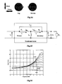
- Some embodiments of the present invention will now be described by way of example and with reference to the accompanying drawings, in which:
- Fig. 1 shows the typical primary and secondary windings of a coreless PCB-based transformer,
- Fig.2 shows the equivalent circuit of a PCB-based transformer with parallel capacitive/resistive load,
- Fig.3 is a plot showing calculated, simulated and measured (a) voltage gain and (b) phase shift of the transformer of Fig. 1 with a capacitive load,
- Fig.4 shows the primary and secondary windings of another coreless PCB-based transformer,
- Fig.5 is a high-frequency equivalent circuit model of the coreless PCB-based transformer of Fig.4,
- Fig.6 is a plot showing predicted (solid-line) and measured (dotted) input impedance against operating frequency of the transformer of Fig.4,
- Figs.7(a) and (b) are plots showing the predicted and measured (a) voltage gain and (b) phase shift,
- Fig.8 is a circuit diagram of a modulated gate drive circuit with smooth duty cycle transition from 0 to 1 known from the prior art,
- Fig.9 is a circuit diagram of a modified modulated gate drive circuit using a coreless PCB-based transformer,
- Figs.10(a) and (b) are plots showing (a) measured input and output signals of the circuit of Fig.9 at fSW = 1Hz, and (b) measured input, carrier and output signals of the circuit of Fig.9 at fSW = 300kHz,
- Figs.11(a) and (b) are plots showing measured Vgs (upper) and Vds (lower) of a power MOSFET at (a) fSWI = 1Hz and (b) fSW = 300kHz,
- Fig.12 is a plot showing measured Vgs (upper) and Id (lower) of the power MOSFET at fSW = 100kHz,
- Fig.13 is a plot showing measured input current of the gate drive circuit against carrier frequency under the worst case condition of duty cycle 1.0,
- Fig.14 shows the primary and secondary windings of another coreless PCB-based transformer,
- Fig.15 shows the equivalent circuit of the transformer of Fig. 14,
- Fig.16 is a plot of the gain of the transformer of Fig.14 against operating frequency with C2 = 100pF,
- Fig.17 is a plot of the input impedance of the coreless PCB-based transformer of Fig.14 against operating frequency with C2 = 100pF,
- Fig.18 is a plot of the energy efficiency of the transformer of Fig.14 against operating frequency with C2 = 100pF,
- Fig.19 is a plot of the gain of the transformer of Fig.14 against operating frequency with C2 = 1000pF,
- Fig.20 is a plot of the input impedance of the transformer of Fig.14 against operating frequency with C2 = 1000pF, and
- Fig.21 is a plot of the energy efficiency of the transformer of Fig.14 against operating frequency with C2 = 1000pF.
-
- A coreless transformer of the type shown in Fig. 1 was fabricated on a PCB and the thickness of the PCB is 1.55 mm. The circuit model (Fig,2) was implemented in PSpice and the circuit equations (1) and (2) (to be discussed later) were also solved in MATLAB [10], the frequency response of the transformer of Fig. 1 is shown in Fig.3, where
- R1 is the primary winding resistance,
- R2' is the secondary winding resistance referred to the primary,
- RL is the resistive load,
- Llk1 is the primary leakage inductance,
- Llk2' is the secondary leakage inductance referred to the primary,
- LM1 is the primary mutual inductance,
- C1 is the primary winding capacitance,
- C2 ' is the secondary winding capacitance referred to the primary,
- C12 is the capacitance between primary and secondary windings, and
- n is the turn ratio.
-
- In general, the voltage gain of the transformer of Fig. 1 is sufficiently high (>0.8 in this example) for gate drive application from 200 kHz to about 5 MHz. Primarily due to the load capacitance and the equivalent leakage inductance of the transformer, resonance occurs at about 5.5 MHz for the transformer of Fig.1. In the Mega-Hertz range below the resonance frequency, the phase shift is very small.
- Observation of this typical frequency response leads to the following important points that can be considered to operate the coreless transformer in an optimal manner:
- (i) The voltage gain of the transformer drops to zero beyond the resonant frequency. Thus the useable frequency range must be below the resonant frequency.
- (ii) The operating frequency of the coreless transformer should be near or at the high-frequency end of the useable operating range (so that the magnetizing reactance is large) in order to minimize the input current and hence the power of the gate drive circuits.
- (iii)Near the resonance region (just below the resonant frequency), the voltage gain is higher than the rest of the operating range. One can take advantage of this high-gain region in order to achieve fast switching time for power MOSFETs or IGBTs.
- (iv)The optimal operating frequency, which combines the benefits of (i) and (ii), should be the frequency at which the impedance of the overall transformer isolated equivalent circuit is at its maximum. At (or near) this maximum-impedance frequency, the power consumption of the coreless PCB transformer gate drive can be minimized.
-
- The dimension of a new coreless PCB transformer is shown in Fig.4. The area of the transfomer in Fig.4 is roughly 25% of that of the transformer of Fig.1, and is much smaller than a typical pulse transformer. Because the intra-winding capacitance of the transformer of Fig.4 is negligible (when measured at 10MHz), the circuit model can be simplified as shown in Fig. 5. The inductive components of the circuit model are calculated by the analytical method proposed by Hurley and Duffy [ W.G.Hurley and MC.Duffy, "Calculation of self and mutual impedances in planar magnetic structures", IEEE Trans. On Magnetics, Vol.31, No.4, July 1995, pp.2416-2422 ] and are also computed using Ansoft 2-dimensional finite-element EM field solver. The width and height of the copper track are 0.22mm and 0.025mm, respectively. The distance between adjacent tracks is about 0.28mm. The number of turns for the primary and secondary printed windings is 10. The interwinding capacitor C12 is calculated by assuming that each coil is a solid conducting plain. The parameters are measured at 10 MHz with a HP 4194A impedance analyzer. The calculated C12 is 3.5pF, which is the same as the measured value. The calculated, computed and measured values of the inductive parameters are listed in Table I. The inductance of the leads connected to the windings is found to be about 36nH. Excluding this external inductance, the corrected measured inductive component values are given in Table I. It is found that these values are in good agreement in general. The difference in the calculated and measured magnetizing inductance is only about 3.3%.
Calculated, computed and measured values for inductive circuit components Hurley and Duffy's method Ansoft Measurements Llk1 267nH 268nH 268nH(+36nH) Llk2 267nH 268nH 268nH (+36nH) Lm 266nH 262nH 275nH - From here onwards, C1 and C2 in the following analysis of optimal gate drive conditions represent the equivalent circuit capacitance that appear in the primary winding and the secondary windings, respectively. Based on this high-frequency model, the voltage gain (V 2 /V 1 ) and the input impedance (Zin, referred to the primary side) of the coreless transformer can be expressed as follows:

- Observation of these plots leads to the following important points:
- 1. The magnitude of the input impedance peaks at a frequency (termed "maximum-impedance frequency") which is within the useable frequency range and is slightly below the resonant frequency. For the transformer of Fig.4, this frequency is about 8 MHz and the impedance is about 150Ω.
- 2. The voltage gain at this "maximum-impedance frequency" is high (about 1.8) and the enlarged outage voltage can speed up the switching times of the power devices. It should be noted that, while the coreless operation has relatively low magnetic coupling than the core-based operation, the use of the resonance technique overcomes such problem and can make the voltage gain greater than unity.
- 3. The phase shift at this frequency is small.
-
- Therefore, this "maximum-impedance frequency" can be chosen as the optimal operating frequency of the coreless PCB transformer if input power consumption has to be minimized. At this frequency, the input power requirement of the gate drive is minimized. It should be noted that this operating frequency is not necessarily the switching frequency of the power devices as will be explained further below. The actual switching frequency depends on the type of the gate drive circuits. If a direct gate drive circuit is used the operating frequency is identical to the switching frequency of the power devices. Direct gate drive circuits using the proposed coreless transformers thus are suitable for a few hundreds of kilo-Hertz to Mega-Hertz switching operation. If the desired switching frequency is less than the operating frequency of the coreless transformer, a modulated gate drive circuit can be used.
- The use of the coreless transformer of Fig.1 in a 'direct' gate drive for operation in the frequency range of a few hundreds of kilo-Hertz and 2 MHz has been described in Hui et al. It has been explained above in the prior art that coreless transformers should be operated at high frequency in the Mega-Hertz range (maximum-impedance frequency). However, the switching frequency in many power electronics circuits ranges from a few Hertz to a few hundreds of kilo-Hertz because of the switching loss constraint. The limitation of the direct gate drive is that it cannot be employed efficiently for switching frequency in the low and medium frequency range (say less than 300kHz). In order to design a coreless transformer isolated gate drive which can be switched in low and medium frequency range, the modulated gate drive circuit such as that described in N.Mohan, T.M.Undeland and W.P.Robbins, Power Electronics: Converters. Applications and Design, Second Edition, John Wiley and Sons Inc. 1995, pp.110-125 can be used. Modulation of a high-frequency carrier by a low-frequency control enables a high-frequency coreless transformer to be used for low frequency switching. Fig.8 shows the simplified schematic of this modulated gate drive that has a smooth transition in the duty cycle from almost zero to one. The energy transfer from the primary side is achieved by the use of a high-frequency carrier signal at the maximum-impedance frequency in the Mega-Hertz range. This minimizes the input current and thus the input power of the gate drive. The control gate signal is coupled to the secondary output by the modulation process.
- Based on the concept of the modulated gate drive, a modified gate drive may be provided that operates the overall coreless transformer gate drive in an optimal manner. Aiming at (i) minimizing the input current requirement and (ii) providing a wide range of switching frequency, the modified gate drive circuit and the test circuit consisting of a resistive-inductive load (5Ω and 1.1mH) are shown in Fig.9. The power MOSFET driven by the modified gate drive is APT5040, which has voltage and current ratings of 500V and 16A respectively. A capacitor of 680pF is conneoted across the secondary winding so that the resonant frequency of the transformer of Fig.4 will be set at about 9.1 MHz. The large stabilizing capacitor of 1µf and the DC blocking capacitor of 0.1µf in the secondary circuit will not significantly affect the frequency characteristic of the transformer because they are in series with a diode (1N4148) which has typical capacitance of only a few pico-Farads. A voltage-doubler is included in the secondary circuit in order to boost the gate drive voltage. The carrier frequency fc (i.e. the operating frequency) is set at 8 MHz which is the "maximum-impedance frequency" of the transformer. The output signal of the gate drive (i.e. the gate-source voltage Vgs of the power MOSFET) is controlled by the input signal Vin of the gate drive in the modulation/demodulation process. Thus, the frequency of Vin determines the switching frequency (fSW ) of the power MOSFET.
- Fig.10a shows the input signal (Vin ) to the gate drive circuit and the gate-source voltage (Vgs ) of the power MOSFET at fSW = 1 Hz. The corresponding waveforms plus the carrier signal (Vc ) at fSW = 300 kHz are shown in Fig.10b. The switching waveforms of the gate-source (Vgs ) and drain-source (Vds ) of the power MOSFET at 1 Hz and 300kHz are shown in Fig.11a and Fig.11b, respectively. Typical switching waveforms of the drain-source voltage Vds and drain current Id of the power MOSFET at a switching frequency of 100kHz are recorded in Fig.12. These practical results confirmed the successfull implementation of the coreless transformer of Fig.4 in the modified modulated gate drive circuit. In order to confirm the minimum input power requirement of the driving conditions, the input current of the gate drive circuit under the condition of 100% duty cycle is measured at various carrier frequencies within the useable frequency range. Under 100% duty cycle, the power consumption of the gate drive is at its maximum (i.e. the worst-case situation). The input current versus carrier frequency under such worst case situation is plotted in Fig.13. It can been seen that the input current is minimum at approximately 8 MHz - the "maximum-impedance frequency" of the transformer in the gate drive design. This result confirms the optimal operating conditions of the proposed gate drive design using the coreless PCB transformer. For a dc voltage supply of 10V used in the primary gate drive circuit, the maximum power consumption of the gate drive under the worst condition is less than 0.9 W.
- When used for energy transfer (such as in a power convener), the coreless PCB transformer is expected to operate at its maximum energy efficiency conditions. Another coreless PCB transformer (shown in Fig.14) is used in this analysis. This transformer has 19 turns in the primary winding and 19 turns in the secondary winding. The thickness of the PCB is 0.4mm. The outer radius of the printed winding is about 5.5mm. This transformer has an equivalent circuit as shown in Fig.15. The parameters of the transformer of Fig.14 are Llk1=0.35595µH; Llk2=0.35595 µH; LM1=1,4936 µH. The effect of C12' is neglected in order to simplify the analysis.
- Power dissipation of the transformer due to the conductor loss is
- In Equation (4), i1 and i2 are the primary and secondary windings currents respectively.where
 Power delivered to the load, ZL, is
- The use of capacitor C2 is to increase the gain (Vs/Vin), input impedance (Zin), and the transformer efficiency (η). The choice of C2 can also determine the resonant frequency of the transformer circuit. In this analysis, a 100pF capacitor C2 is connected in parallel with the secondary winding of the transformer. The gain (Vs/Vin), input impedance (Zin), and the efficiency (η), of the transformer versus operating frequency are plotted in Fig.16 to Fig.18, respectively. The load resistance (RL) varies from 50Ω to 500Ω with 50Ω incremental step.
- With C2=100pF, Fig.16 shows that the resonant frequency of the transformer of Fig.14 is greater than 15MHz (around 18MHz to 19MHz depending on the load resistance). Fig.17 indicates that the maximum impedance frequency (MIF) occurs at around 11 MHz. The efficiency curves for various load resistances are plotted in Fig.18. It can be seen that the maximum efficiency frequency (MEF) is slightly less than the MIF (around 9MHz to 10MHz). In fact, the transformer can be operated with the frequency range of 8MHz to 11MHz in order to achieve high efficiency (say >90%).
- When the load resistance is very large, i.e. load power is very low, the load current and i2 are very small that the power dissipation of the transformer is dominated by i2R loss component due to the current i1 . On the other hand, increasing the transformer input impedance reduces the primary winding curent, i1. Thus, the MEF tends to MIF as the load current is small. For example, power consumption of MOSFET/IGBT gate drive circuits is small enough that the MEF is regarded as the MIF.
- When the load resistance decreases, i.e. load power increases, Equation (4) shows that the increasing secondary winding current, i2, will increase the transformer i2R loss. From Equation (5), the winding resistance increases as operating frequency increases. As a result, operating the transformer in lower frequency can reduce the power loss of the transformer when i2 is significant. As shown in Fig.18, the MEF is below the MIF. MEF increases when the load resistance increases (i.e. the load power decreases).
- The transformer of Fig.14 is also studied with a larger capacitance C2. As the C2 increases, the voltage gain, resonance frequency, MIF and the MEF decrease. An example with C2=1000pF is used to illustrate the phenomena Fig.19 to Fig.21 show the frequency response of the gain (Vs/Vin), input impedance (Zin) and the efficiency (η) of the transformer, respectively. The resonant frequency is now set at about 6MHz. The MIF is about 3.8MHz and the MEF is about 3.2MHz. Thus, the coreless PCB transformer, when used in a power converter, should be operated at the MEF (which is lower than the MIF) in order to achieve maximum energy efficiency.
- It will thus be Been that optimal operating techniques for using a coreless PCB transfomer under (1) minimum input power requirement and (2) maximum energy efficiency have been described above. The optimal operation of a coreless PCB transformer in an isolated gate drive circuits for power MOSFET/IGBT devices has been successfully demonstrated for a wide frequency range from 1 Hz to 300 kHz. Criteria for selecting the optimal operating conditions for the coreless transformer in gate drive (energy and signal transfer) applications are developed, presented and experimentally verified. It is found that coreless transformers should be operated at or near their "maximum-impedance frequencies" so that the input power requirement can be minimized and the voltage gain is high. This optimal operating condition of the coreless transformer has been demonstrated in the "modulated" gate drive circuit and can also be applied to the "direct" gate drive. For both types of isolated gate drive circuits, the operating frequency of the transformers are always chosen to their "maximum-impedance frequencies". For the modulated transformer-isolated gate drive circuit, the carrier frequency of the transformer circuit is chosen to be the maximum-impedance frequency of the transformer. The transmitted signal (which has a frequency lower than the carrier frequency) can be recovered in the demodulation process. For the direct gate drive, the signal is simply transmitted at the maximum-impedance frequency of the transformer. The choice of optimal operating frequency of the transformer circuit can be very flexible because the resonant frequency and thus the maximum-impedance frequency of the transformer circuit can be precisely determined by the size of the external capacitor C2. Procedures for selecting the parameters for the modulated gate drive have also been described above. When used with coreless transformers, direct gate drives are found to be suitable for high (Mega-Hertz) switching frequency. The modulated gate drive should be used for low and medium (say less than 300kHz) switching operation. The size of the new coreless transformer of Fig.4 is about 25% of that of a previously known transformer and is much smaller than that of a typical core-based high-frequency pulse transformer in terms of both area and volume.
- When used for electrical energy transfer such as in a power converter, the coreless PCB transformers should be operated at or near their maximum efficiency frequency (MEF) which is found to be lower than the maximum impedance frequency (MIF).
- Coreless transformers are cheaper than core-based transformers. They eliminate the requirements of magnetic core and manually-wound transformers. Consequently, automation in the manufacturing process of gate drive circuits becomes feasible and the manufacturing cost can be reduced. In conclusion, it is demonstrated that magnetic core is not a necessary item in transformer isolated gate drive circuits. The same idea can, in principle, be applied to low-power converters. Coreless PCB transformers are particularly suitable for use in applications in which stringent height requirements have to be met.
Claims (10)
- A coreless printed circuit board transformer comprising first and second windings deposited on opposed sides of a printed circuit board and having no transformer core therebetween, wherein said transformer is operated at an optimum frequency which is at or near the frequency at which the impedance of a transformer equivalent circuit is at its maximum.
- A transformer as claimed in claim 1 wherein said transformer is operated at a frequency of bout 100kHz to at least 20MHz.
- A transformer as claimed in claim 1 wherein said transformer is operated by a high-frequency carrier signal modulated by a low-frequency switching signal, said carrier signal being at a frequency corresponding to the maximum impedance of the transformer.
- A transformer as claimed in claim 3 wherein said carrier signal is at a frequency of about 100kHz to at least 20MHz and said switching signal is at a frequency of between DC and 300kHz.
- A gate drive circuit for a power MOSFET or IGBT device, wherein the gate of said device is isolated from an input power supply by a coreless printed circuit board transformer as claimed in any of claims 1 to 4.
- A method of driving a gate of a power MOSFET or IGBT device comprising isolating said gate from a power supply by means of a coreless printed circuit board transformer, said transformer comprising first and second windings deposited on opposed sides of a printed circuit board with no transformer core therebetween, wherein said gate is driven at a frequency at which the impedance of said transformer is at a maximum.
- A method as claimed in claim 6 wherein said gate is driven at a frequency in the range of from about 100kHz to at least 20MHz.
- A method as claimed in claim 6 wherein a low frequency switching signal is used to modulate a high-frequency carrier signal input to said transformer, and wherein said carrier signal is demodulated after said transformer to drive said gate at said low switching frequency, said carrier signal being at a said maximum impedance frequency.
- A method as claimed in claim 8 wherein said carrier signal is at a frequency of from about 100kHz to at least 20MHz and said switching signal is at a frequency of from DC to 300kHz.
- Power converter apparatus including a coreless printed circuit board transformer comprising first and second windings deposited on opposed sides of a printed circuit board and having no transformer core therebetween, wherein said transformer is operated at a maximum efficiency frequency which is slightly lower than the frequency at which the impedance of a transformer equivalent circuit is at its maximum.
Applications Claiming Priority (2)
| Application Number | Priority Date | Filing Date | Title |
|---|---|---|---|
| US1887198A | 1998-02-05 | 1998-02-05 | |
| US18871 | 1998-02-05 |
Publications (3)
| Publication Number | Publication Date |
|---|---|
| EP0935263A2 true EP0935263A2 (en) | 1999-08-11 |
| EP0935263A3 EP0935263A3 (en) | 1999-12-15 |
| EP0935263B1 EP0935263B1 (en) | 2004-05-26 |
Family
ID=21790194
Family Applications (1)
| Application Number | Title | Priority Date | Filing Date |
|---|---|---|---|
| EP99300789A Expired - Lifetime EP0935263B1 (en) | 1998-02-05 | 1999-02-03 | Method of operating a coreless printed-circuit-board (PCB) transformer |
Country Status (4)
| Country | Link |
|---|---|
| EP (1) | EP0935263B1 (en) |
| CN (1) | CN1240085C (en) |
| AT (1) | ATE268050T1 (en) |
| DE (1) | DE69917504T2 (en) |
Cited By (24)
| Publication number | Priority date | Publication date | Assignee | Title |
|---|---|---|---|---|
| US7042325B2 (en) | 2002-05-31 | 2006-05-09 | International Rectifier Corporation | Planar transformer arrangement |
| DE102005004406A1 (en) * | 2005-01-31 | 2006-08-10 | Schwille Elektronik Produktions- Und Vertriebs Gmbh | Electrical coil e.g. flat spiral coil, for use in frame of tesla generator, has windings lying next to each other in plane, radially connected together and out-etched from electrically conducting layer of plate |
| WO2006111631A1 (en) * | 2005-04-20 | 2006-10-26 | Ciprian | Electric signal amplifier for ultrasound applications |
| EP2007023A2 (en) | 2007-06-18 | 2008-12-24 | Insta Elektro GmbH | Installation device |
| EP2007009A2 (en) | 2007-06-15 | 2008-12-24 | City University of Hong Kong | Planar emi filter |
| US7495414B2 (en) | 2005-07-25 | 2009-02-24 | Convenient Power Limited | Rechargeable battery circuit and structure for compatibility with a planar inductive charging platform |
| US7978041B2 (en) | 2009-04-16 | 2011-07-12 | Seps Technologies Ab | Transformer |
| US8120445B2 (en) | 2007-06-15 | 2012-02-21 | City University Of Hong Kong | Planar EMI filter comprising coreless spiral planar windings |
| CN105932789A (en) * | 2016-05-10 | 2016-09-07 | 京东方科技集团股份有限公司 | Transformer and power strip |
| US9642219B2 (en) | 2014-06-05 | 2017-05-02 | Steelcase Inc. | Environment optimization for space based on presence and activities |
| US9852388B1 (en) | 2014-10-03 | 2017-12-26 | Steelcase, Inc. | Method and system for locating resources and communicating within an enterprise |
| US9921726B1 (en) | 2016-06-03 | 2018-03-20 | Steelcase Inc. | Smart workstation method and system |
| US9955318B1 (en) | 2014-06-05 | 2018-04-24 | Steelcase Inc. | Space guidance and management system and method |
| US10161752B1 (en) | 2014-10-03 | 2018-12-25 | Steelcase Inc. | Method and system for locating resources and communicating within an enterprise |
| PL422409A1 (en) * | 2017-07-31 | 2019-02-11 | ABB Spółka z ograniczoną odpowiedzialnością | High-frequency winding from PCB printed circuits |
| US10264213B1 (en) | 2016-12-15 | 2019-04-16 | Steelcase Inc. | Content amplification system and method |
| US10353664B2 (en) | 2014-03-07 | 2019-07-16 | Steelcase Inc. | Method and system for facilitating collaboration sessions |
| US10433646B1 (en) | 2014-06-06 | 2019-10-08 | Steelcaase Inc. | Microclimate control systems and methods |
| WO2020020394A3 (en) * | 2018-07-22 | 2020-03-26 | Kiefel Gmbh | Device and method for operating an impedance-variable load at the planar transformer in high-frequency operation i |
| US10614694B1 (en) | 2014-06-06 | 2020-04-07 | Steelcase Inc. | Powered furniture assembly |
| US10733371B1 (en) | 2015-06-02 | 2020-08-04 | Steelcase Inc. | Template based content preparation system for use with a plurality of space types |
| US11321643B1 (en) | 2014-03-07 | 2022-05-03 | Steelcase Inc. | Method and system for facilitating collaboration sessions |
| US11744376B2 (en) | 2014-06-06 | 2023-09-05 | Steelcase Inc. | Microclimate control systems and methods |
| US11956838B1 (en) | 2023-05-08 | 2024-04-09 | Steelcase Inc. | Smart workstation method and system |
Families Citing this family (9)
| Publication number | Priority date | Publication date | Assignee | Title |
|---|---|---|---|---|
| DE102004019447A1 (en) * | 2004-04-19 | 2005-11-10 | Siemens Ag | Device, in particular intelligent power module, with planar connection technology |
| US7948067B2 (en) | 2009-06-30 | 2011-05-24 | Avago Technologies Ecbu Ip (Singapore) Pte. Ltd. | Coil transducer isolator packages |
| US8061017B2 (en) | 2006-08-28 | 2011-11-22 | Avago Technologies Ecbu Ip (Singapore) Pte. Ltd. | Methods of making coil transducers |
| US8093983B2 (en) | 2006-08-28 | 2012-01-10 | Avago Technologies Ecbu Ip (Singapore) Pte. Ltd. | Narrowbody coil isolator |
| US7852186B2 (en) | 2006-08-28 | 2010-12-14 | Avago Technologies Ecbu Ip (Singapore) Pte. Ltd. | Coil transducer with reduced arcing and improved high voltage breakdown performance characteristics |
| US7791900B2 (en) | 2006-08-28 | 2010-09-07 | Avago Technologies General Ip (Singapore) Pte. Ltd. | Galvanic isolator |
| US9117586B2 (en) | 2009-03-09 | 2015-08-25 | Infineon Technologies Austria Ag | Trimmable transformer arrangement |
| US20140210279A1 (en) * | 2011-08-16 | 2014-07-31 | Koninklijke Philips N.V. | Laminate surface for wireless capacitive power |
| CN104104348A (en) * | 2014-08-01 | 2014-10-15 | 王少夫 | Adjustable printing plate transformer |
Citations (2)
| Publication number | Priority date | Publication date | Assignee | Title |
|---|---|---|---|---|
| EP0147499A2 (en) * | 1983-03-16 | 1985-07-10 | N.V. Machiels-Hanot | Broadband impedance transformer and resonator |
| JPH0410680A (en) * | 1990-04-27 | 1992-01-14 | Matsushita Electric Ind Co Ltd | Gas laser apparatus |
-
1999
- 1999-02-03 AT AT99300789T patent/ATE268050T1/en not_active IP Right Cessation
- 1999-02-03 DE DE69917504T patent/DE69917504T2/en not_active Expired - Lifetime
- 1999-02-03 EP EP99300789A patent/EP0935263B1/en not_active Expired - Lifetime
- 1999-02-04 CN CN99100579.1A patent/CN1240085C/en not_active Expired - Lifetime
Patent Citations (2)
| Publication number | Priority date | Publication date | Assignee | Title |
|---|---|---|---|---|
| EP0147499A2 (en) * | 1983-03-16 | 1985-07-10 | N.V. Machiels-Hanot | Broadband impedance transformer and resonator |
| JPH0410680A (en) * | 1990-04-27 | 1992-01-14 | Matsushita Electric Ind Co Ltd | Gas laser apparatus |
Non-Patent Citations (2)
| Title |
|---|
| HUI S Y R ET AL: "Coreless PCB-based transformers for power MOSFET/IGBT gate drive circuits" PEPSC97 RECORD. 28TH ANNUAL IEEE POWER ELECTRONICS SPECIALISTS CONFERENCE (CAT. NO.97CH36043), PESC97. RECORD 28TH ANNUAL IEEE POWER ELECTRONICS SPECIALISTS CONFERENCE. FORMERLY POWER CONDITIONING SPECIALISTS CONFERENCE 1970-71. POWER PROCESSING AND , pages 1171-1176 vol.2, XP002118944 1997, New York, NY, USA, IEEE, USA ISBN: 0-7803-3840-5 * |
| PATENT ABSTRACTS OF JAPAN vol. 016, no. 158 (E-1191), 17 April 1992 (1992-04-17) & JP 04 010680 A (MATSUSHITA ELECTRIC IND CO LTD), 14 January 1992 (1992-01-14) * |
Cited By (52)
| Publication number | Priority date | Publication date | Assignee | Title |
|---|---|---|---|---|
| US7042325B2 (en) | 2002-05-31 | 2006-05-09 | International Rectifier Corporation | Planar transformer arrangement |
| DE102005004406A1 (en) * | 2005-01-31 | 2006-08-10 | Schwille Elektronik Produktions- Und Vertriebs Gmbh | Electrical coil e.g. flat spiral coil, for use in frame of tesla generator, has windings lying next to each other in plane, radially connected together and out-etched from electrically conducting layer of plate |
| WO2006111631A1 (en) * | 2005-04-20 | 2006-10-26 | Ciprian | Electric signal amplifier for ultrasound applications |
| US7495414B2 (en) | 2005-07-25 | 2009-02-24 | Convenient Power Limited | Rechargeable battery circuit and structure for compatibility with a planar inductive charging platform |
| EP2007009A3 (en) * | 2007-06-15 | 2009-12-02 | City University of Hong Kong | Planar emi filter |
| US8120445B2 (en) | 2007-06-15 | 2012-02-21 | City University Of Hong Kong | Planar EMI filter comprising coreless spiral planar windings |
| EP2007009A2 (en) | 2007-06-15 | 2008-12-24 | City University of Hong Kong | Planar emi filter |
| EP2007023A3 (en) * | 2007-06-18 | 2010-10-06 | Insta Elektro GmbH | Installation device |
| EP2007023A2 (en) | 2007-06-18 | 2008-12-24 | Insta Elektro GmbH | Installation device |
| US7978041B2 (en) | 2009-04-16 | 2011-07-12 | Seps Technologies Ab | Transformer |
| US11321643B1 (en) | 2014-03-07 | 2022-05-03 | Steelcase Inc. | Method and system for facilitating collaboration sessions |
| US11150859B2 (en) | 2014-03-07 | 2021-10-19 | Steelcase Inc. | Method and system for facilitating collaboration sessions |
| US10353664B2 (en) | 2014-03-07 | 2019-07-16 | Steelcase Inc. | Method and system for facilitating collaboration sessions |
| US11280619B1 (en) | 2014-06-05 | 2022-03-22 | Steelcase Inc. | Space guidance and management system and method |
| US9642219B2 (en) | 2014-06-05 | 2017-05-02 | Steelcase Inc. | Environment optimization for space based on presence and activities |
| US10057963B2 (en) | 2014-06-05 | 2018-08-21 | Steelcase Inc. | Environment optimization for space based on presence and activities |
| US11402216B1 (en) | 2014-06-05 | 2022-08-02 | Steelcase Inc. | Space guidance and management system and method |
| US11402217B1 (en) | 2014-06-05 | 2022-08-02 | Steelcase Inc. | Space guidance and management system and method |
| US11307037B1 (en) | 2014-06-05 | 2022-04-19 | Steelcase Inc. | Space guidance and management system and method |
| US10225707B1 (en) | 2014-06-05 | 2019-03-05 | Steelcase Inc. | Space guidance and management system and method |
| US9955318B1 (en) | 2014-06-05 | 2018-04-24 | Steelcase Inc. | Space guidance and management system and method |
| US11085771B1 (en) | 2014-06-05 | 2021-08-10 | Steelcase Inc. | Space guidance and management system and method |
| US10561006B2 (en) | 2014-06-05 | 2020-02-11 | Steelcase Inc. | Environment optimization for space based on presence and activities |
| US11212898B2 (en) | 2014-06-05 | 2021-12-28 | Steelcase Inc. | Environment optimization for space based on presence and activities |
| US10433646B1 (en) | 2014-06-06 | 2019-10-08 | Steelcaase Inc. | Microclimate control systems and methods |
| US11744376B2 (en) | 2014-06-06 | 2023-09-05 | Steelcase Inc. | Microclimate control systems and methods |
| US10614694B1 (en) | 2014-06-06 | 2020-04-07 | Steelcase Inc. | Powered furniture assembly |
| US9852388B1 (en) | 2014-10-03 | 2017-12-26 | Steelcase, Inc. | Method and system for locating resources and communicating within an enterprise |
| US11168987B2 (en) | 2014-10-03 | 2021-11-09 | Steelcase Inc. | Method and system for locating resources and communicating within an enterprise |
| US10161752B1 (en) | 2014-10-03 | 2018-12-25 | Steelcase Inc. | Method and system for locating resources and communicating within an enterprise |
| US10970662B2 (en) | 2014-10-03 | 2021-04-06 | Steelcase Inc. | Method and system for locating resources and communicating within an enterprise |
| US10121113B1 (en) | 2014-10-03 | 2018-11-06 | Steelcase Inc. | Method and system for locating resources and communicating within an enterprise |
| US11713969B1 (en) | 2014-10-03 | 2023-08-01 | Steelcase Inc. | Method and system for locating resources and communicating within an enterprise |
| US11143510B1 (en) | 2014-10-03 | 2021-10-12 | Steelcase Inc. | Method and system for locating resources and communicating within an enterprise |
| US11687854B1 (en) | 2014-10-03 | 2023-06-27 | Steelcase Inc. | Method and system for locating resources and communicating within an enterprise |
| US10733371B1 (en) | 2015-06-02 | 2020-08-04 | Steelcase Inc. | Template based content preparation system for use with a plurality of space types |
| US11100282B1 (en) | 2015-06-02 | 2021-08-24 | Steelcase Inc. | Template based content preparation system for use with a plurality of space types |
| CN105932789B (en) * | 2016-05-10 | 2021-04-27 | 京东方科技集团股份有限公司 | Transformer and power panel |
| US10644541B2 (en) | 2016-05-10 | 2020-05-05 | Boe Technology Group Co., Ltd. | Transformer and power supply board |
| CN105932789A (en) * | 2016-05-10 | 2016-09-07 | 京东方科技集团股份有限公司 | Transformer and power strip |
| US11690111B1 (en) | 2016-06-03 | 2023-06-27 | Steelcase Inc. | Smart workstation method and system |
| US10459611B1 (en) | 2016-06-03 | 2019-10-29 | Steelcase Inc. | Smart workstation method and system |
| US9921726B1 (en) | 2016-06-03 | 2018-03-20 | Steelcase Inc. | Smart workstation method and system |
| US11330647B2 (en) | 2016-06-03 | 2022-05-10 | Steelcase Inc. | Smart workstation method and system |
| US10264213B1 (en) | 2016-12-15 | 2019-04-16 | Steelcase Inc. | Content amplification system and method |
| US11652957B1 (en) | 2016-12-15 | 2023-05-16 | Steelcase Inc. | Content amplification system and method |
| US11190731B1 (en) | 2016-12-15 | 2021-11-30 | Steelcase Inc. | Content amplification system and method |
| US10638090B1 (en) | 2016-12-15 | 2020-04-28 | Steelcase Inc. | Content amplification system and method |
| US10897598B1 (en) | 2016-12-15 | 2021-01-19 | Steelcase Inc. | Content amplification system and method |
| PL422409A1 (en) * | 2017-07-31 | 2019-02-11 | ABB Spółka z ograniczoną odpowiedzialnością | High-frequency winding from PCB printed circuits |
| WO2020020394A3 (en) * | 2018-07-22 | 2020-03-26 | Kiefel Gmbh | Device and method for operating an impedance-variable load at the planar transformer in high-frequency operation i |
| US11956838B1 (en) | 2023-05-08 | 2024-04-09 | Steelcase Inc. | Smart workstation method and system |
Also Published As
| Publication number | Publication date |
|---|---|
| DE69917504D1 (en) | 2004-07-01 |
| CN1240085C (en) | 2006-02-01 |
| EP0935263A3 (en) | 1999-12-15 |
| ATE268050T1 (en) | 2004-06-15 |
| DE69917504T2 (en) | 2005-06-23 |
| CN1237081A (en) | 1999-12-01 |
| EP0935263B1 (en) | 2004-05-26 |
Similar Documents
| Publication | Publication Date | Title |
|---|---|---|
| EP0935263B1 (en) | Method of operating a coreless printed-circuit-board (PCB) transformer | |
| US8102235B2 (en) | Coreless printed-circuit-board (PCB) transformers and operating techniques therefor | |
| US10985740B2 (en) | High voltage nanosecond pulser with variable pulse width and pulse repetition frequency | |
| US8772909B1 (en) | Isolator with integral transformer | |
| US5990776A (en) | Low noise full integrated multilayers magnetic for power converters | |
| US7123123B2 (en) | High-frequency power transformer | |
| EP0917163B1 (en) | Magnetic component assembly | |
| Hui et al. | Coreless printed circuit board (PCB) transformers for power MOSFET/IGBT gate drive circuits | |
| Ali et al. | Integrated active filter for differential-mode noise suppression | |
| US10790080B2 (en) | Embedded magnetic component transformer device | |
| EP3167549A1 (en) | High voltage nanosecond pulser with variable pulse width and pulse repetition frequency | |
| Tang et al. | Coreless printed circuit board (PCB) transformers with multiple secondary windings for complementary gate drive circuits | |
| WO2005034319A1 (en) | Ripple-current reduction for transformers | |
| US9508485B1 (en) | Isolator with integral transformer | |
| Bharath et al. | Design of isolated gate driver power supply in medium voltage converters using high frequency and compact wireless power transfer | |
| Zeltner | Insulating IGBT driver with PCB integrated capacitive coupling elements | |
| Sato et al. | 5 MHz switching micro dc-dc converter using planar inductor | |
| US7161457B2 (en) | Common mode choke including conductors within dielectric layer and associated methods | |
| CN110868078B (en) | Symmetrical half-bridge LC series resonance sine power conversion circuit | |
| Hui et al. | Coreless Printed Circuit Board (PCB) Transformers-Fundamental Characteristics and Application Potential | |
| CN114520109A (en) | Symmetrical split transformer for reducing EMI | |
| Wang et al. | Evaluation of LTCC capacitors and inductors in DC/DC converters | |
| Bakar et al. | High frequency (MHz) soft switched flyback dc-dc converter using GaN switches and six-layered PCB transformer | |
| Weis et al. | PCB Embedded Transformer for Isolated DC-DC Power Supplies | |
| Waffenschmidt et al. | Planar resonant multi-output transformer for printed circuit board integration |
Legal Events
| Date | Code | Title | Description |
|---|---|---|---|
| PUAI | Public reference made under article 153(3) epc to a published international application that has entered the european phase |
Free format text: ORIGINAL CODE: 0009012 |
|
| AK | Designated contracting states |
Kind code of ref document: A2 Designated state(s): AT CH DE DK FI FR GB IE IT LI SE |
|
| AX | Request for extension of the european patent |
Free format text: AL;LT;LV;MK;RO;SI |
|
| PUAL | Search report despatched |
Free format text: ORIGINAL CODE: 0009013 |
|
| RIC1 | Information provided on ipc code assigned before grant |
Free format text: 6H 01F 19/04 A, 6H 01F 27/28 B, 6H 03H 7/38 B |
|
| AK | Designated contracting states |
Kind code of ref document: A3 Designated state(s): AT BE CH CY DE DK ES FI FR GB GR IE IT LI LU MC NL PT SE |
|
| AX | Request for extension of the european patent |
Free format text: AL;LT;LV;MK;RO;SI |
|
| 17P | Request for examination filed |
Effective date: 20000324 |
|
| AKX | Designation fees paid |
Free format text: AT CH DE DK FI FR GB IE IT LI SE |
|
| 17Q | First examination report despatched |
Effective date: 20021204 |
|
| RTI1 | Title (correction) |
Free format text: METHOD OF OPERATING A CORELESS PRINTED-CIRCUIT-BOARD (PCB) TRANSFORMER |
|
| GRAP | Despatch of communication of intention to grant a patent |
Free format text: ORIGINAL CODE: EPIDOSNIGR1 |
|
| GRAS | Grant fee paid |
Free format text: ORIGINAL CODE: EPIDOSNIGR3 |
|
| GRAA | (expected) grant |
Free format text: ORIGINAL CODE: 0009210 |
|
| AK | Designated contracting states |
Kind code of ref document: B1 Designated state(s): AT CH DE DK FI FR GB IE IT LI SE |
|
| PG25 | Lapsed in a contracting state [announced via postgrant information from national office to epo] |
Ref country code: LI Free format text: LAPSE BECAUSE OF FAILURE TO SUBMIT A TRANSLATION OF THE DESCRIPTION OR TO PAY THE FEE WITHIN THE PRESCRIBED TIME-LIMIT Effective date: 20040526 Ref country code: IT Free format text: LAPSE BECAUSE OF FAILURE TO SUBMIT A TRANSLATION OF THE DESCRIPTION OR TO PAY THE FEE WITHIN THE PRESCRIBED TIME-LIMIT;WARNING: LAPSES OF ITALIAN PATENTS WITH EFFECTIVE DATE BEFORE 2007 MAY HAVE OCCURRED AT ANY TIME BEFORE 2007. THE CORRECT EFFECTIVE DATE MAY BE DIFFERENT FROM THE ONE RECORDED. Effective date: 20040526 Ref country code: FR Free format text: LAPSE BECAUSE OF NON-PAYMENT OF DUE FEES Effective date: 20040526 Ref country code: FI Free format text: LAPSE BECAUSE OF FAILURE TO SUBMIT A TRANSLATION OF THE DESCRIPTION OR TO PAY THE FEE WITHIN THE PRESCRIBED TIME-LIMIT Effective date: 20040526 Ref country code: CH Free format text: LAPSE BECAUSE OF FAILURE TO SUBMIT A TRANSLATION OF THE DESCRIPTION OR TO PAY THE FEE WITHIN THE PRESCRIBED TIME-LIMIT Effective date: 20040526 Ref country code: AT Free format text: LAPSE BECAUSE OF FAILURE TO SUBMIT A TRANSLATION OF THE DESCRIPTION OR TO PAY THE FEE WITHIN THE PRESCRIBED TIME-LIMIT Effective date: 20040526 |
|
| RAP1 | Party data changed (applicant data changed or rights of an application transferred) |
Owner name: CITY UNIVERSITY OF HONG KONG |
|
| REG | Reference to a national code |
Ref country code: GB Ref legal event code: FG4D |
|
| REG | Reference to a national code |
Ref country code: CH Ref legal event code: EP |
|
| REG | Reference to a national code |
Ref country code: IE Ref legal event code: FG4D |
|
| REF | Corresponds to: |
Ref document number: 69917504 Country of ref document: DE Date of ref document: 20040701 Kind code of ref document: P |
|
| PG25 | Lapsed in a contracting state [announced via postgrant information from national office to epo] |
Ref country code: SE Free format text: LAPSE BECAUSE OF FAILURE TO SUBMIT A TRANSLATION OF THE DESCRIPTION OR TO PAY THE FEE WITHIN THE PRESCRIBED TIME-LIMIT Effective date: 20040826 Ref country code: DK Free format text: LAPSE BECAUSE OF FAILURE TO SUBMIT A TRANSLATION OF THE DESCRIPTION OR TO PAY THE FEE WITHIN THE PRESCRIBED TIME-LIMIT Effective date: 20040826 |
|
| REG | Reference to a national code |
Ref country code: CH Ref legal event code: PL |
|
| PG25 | Lapsed in a contracting state [announced via postgrant information from national office to epo] |
Ref country code: IE Free format text: LAPSE BECAUSE OF NON-PAYMENT OF DUE FEES Effective date: 20050203 |
|
| PGFP | Annual fee paid to national office [announced via postgrant information from national office to epo] |
Ref country code: FR Payment date: 20050208 Year of fee payment: 7 |
|
| PLBE | No opposition filed within time limit |
Free format text: ORIGINAL CODE: 0009261 |
|
| STAA | Information on the status of an ep patent application or granted ep patent |
Free format text: STATUS: NO OPPOSITION FILED WITHIN TIME LIMIT |
|
| 26N | No opposition filed |
Effective date: 20050301 |
|
| EN | Fr: translation not filed | ||
| REG | Reference to a national code |
Ref country code: IE Ref legal event code: MM4A |
|
| REG | Reference to a national code |
Ref country code: GB Ref legal event code: 732E |
|
| PGFP | Annual fee paid to national office [announced via postgrant information from national office to epo] |
Ref country code: DE Payment date: 20180123 Year of fee payment: 20 Ref country code: GB Payment date: 20180131 Year of fee payment: 20 |
|
| REG | Reference to a national code |
Ref country code: DE Ref legal event code: R071 Ref document number: 69917504 Country of ref document: DE |
|
| REG | Reference to a national code |
Ref country code: GB Ref legal event code: PE20 Expiry date: 20190202 |
|
| PG25 | Lapsed in a contracting state [announced via postgrant information from national office to epo] |
Ref country code: GB Free format text: LAPSE BECAUSE OF EXPIRATION OF PROTECTION Effective date: 20190202 |