EP0936282A2 - Low-k fluorinated amorphous carbon dielectric and method of making the same - Google Patents
Low-k fluorinated amorphous carbon dielectric and method of making the same Download PDFInfo
- Publication number
- EP0936282A2 EP0936282A2 EP99300444A EP99300444A EP0936282A2 EP 0936282 A2 EP0936282 A2 EP 0936282A2 EP 99300444 A EP99300444 A EP 99300444A EP 99300444 A EP99300444 A EP 99300444A EP 0936282 A2 EP0936282 A2 EP 0936282A2
- Authority
- EP
- European Patent Office
- Prior art keywords
- pecvd
- chamber
- substrate
- silane
- generally
- Prior art date
- Legal status (The legal status is an assumption and is not a legal conclusion. Google has not performed a legal analysis and makes no representation as to the accuracy of the status listed.)
- Granted
Links
Images
Classifications
-
- H—ELECTRICITY
- H01—ELECTRIC ELEMENTS
- H01L—SEMICONDUCTOR DEVICES NOT COVERED BY CLASS H10
- H01L21/00—Processes or apparatus adapted for the manufacture or treatment of semiconductor or solid state devices or of parts thereof
- H01L21/02—Manufacture or treatment of semiconductor devices or of parts thereof
- H01L21/04—Manufacture or treatment of semiconductor devices or of parts thereof the devices having at least one potential-jump barrier or surface barrier, e.g. PN junction, depletion layer or carrier concentration layer
- H01L21/18—Manufacture or treatment of semiconductor devices or of parts thereof the devices having at least one potential-jump barrier or surface barrier, e.g. PN junction, depletion layer or carrier concentration layer the devices having semiconductor bodies comprising elements of Group IV of the Periodic System or AIIIBV compounds with or without impurities, e.g. doping materials
- H01L21/20—Deposition of semiconductor materials on a substrate, e.g. epitaxial growth solid phase epitaxy
-
- H—ELECTRICITY
- H01—ELECTRIC ELEMENTS
- H01L—SEMICONDUCTOR DEVICES NOT COVERED BY CLASS H10
- H01L21/00—Processes or apparatus adapted for the manufacture or treatment of semiconductor or solid state devices or of parts thereof
- H01L21/02—Manufacture or treatment of semiconductor devices or of parts thereof
- H01L21/02104—Forming layers
- H01L21/02107—Forming insulating materials on a substrate
- H01L21/02225—Forming insulating materials on a substrate characterised by the process for the formation of the insulating layer
- H01L21/0226—Forming insulating materials on a substrate characterised by the process for the formation of the insulating layer formation by a deposition process
- H01L21/02263—Forming insulating materials on a substrate characterised by the process for the formation of the insulating layer formation by a deposition process deposition from the gas or vapour phase
- H01L21/02271—Forming insulating materials on a substrate characterised by the process for the formation of the insulating layer formation by a deposition process deposition from the gas or vapour phase deposition by decomposition or reaction of gaseous or vapour phase compounds, i.e. chemical vapour deposition
- H01L21/02274—Forming insulating materials on a substrate characterised by the process for the formation of the insulating layer formation by a deposition process deposition from the gas or vapour phase deposition by decomposition or reaction of gaseous or vapour phase compounds, i.e. chemical vapour deposition in the presence of a plasma [PECVD]
-
- C—CHEMISTRY; METALLURGY
- C23—COATING METALLIC MATERIAL; COATING MATERIAL WITH METALLIC MATERIAL; CHEMICAL SURFACE TREATMENT; DIFFUSION TREATMENT OF METALLIC MATERIAL; COATING BY VACUUM EVAPORATION, BY SPUTTERING, BY ION IMPLANTATION OR BY CHEMICAL VAPOUR DEPOSITION, IN GENERAL; INHIBITING CORROSION OF METALLIC MATERIAL OR INCRUSTATION IN GENERAL
- C23C—COATING METALLIC MATERIAL; COATING MATERIAL WITH METALLIC MATERIAL; SURFACE TREATMENT OF METALLIC MATERIAL BY DIFFUSION INTO THE SURFACE, BY CHEMICAL CONVERSION OR SUBSTITUTION; COATING BY VACUUM EVAPORATION, BY SPUTTERING, BY ION IMPLANTATION OR BY CHEMICAL VAPOUR DEPOSITION, IN GENERAL
- C23C16/00—Chemical coating by decomposition of gaseous compounds, without leaving reaction products of surface material in the coating, i.e. chemical vapour deposition [CVD] processes
- C23C16/22—Chemical coating by decomposition of gaseous compounds, without leaving reaction products of surface material in the coating, i.e. chemical vapour deposition [CVD] processes characterised by the deposition of inorganic material, other than metallic material
- C23C16/26—Deposition of carbon only
-
- H—ELECTRICITY
- H01—ELECTRIC ELEMENTS
- H01L—SEMICONDUCTOR DEVICES NOT COVERED BY CLASS H10
- H01L21/00—Processes or apparatus adapted for the manufacture or treatment of semiconductor or solid state devices or of parts thereof
- H01L21/02—Manufacture or treatment of semiconductor devices or of parts thereof
- H01L21/02104—Forming layers
- H01L21/02107—Forming insulating materials on a substrate
- H01L21/02109—Forming insulating materials on a substrate characterised by the type of layer, e.g. type of material, porous/non-porous, pre-cursors, mixtures or laminates
- H01L21/02112—Forming insulating materials on a substrate characterised by the type of layer, e.g. type of material, porous/non-porous, pre-cursors, mixtures or laminates characterised by the material of the layer
- H01L21/02115—Forming insulating materials on a substrate characterised by the type of layer, e.g. type of material, porous/non-porous, pre-cursors, mixtures or laminates characterised by the material of the layer the material being carbon, e.g. alpha-C, diamond or hydrogen doped carbon
-
- H—ELECTRICITY
- H01—ELECTRIC ELEMENTS
- H01L—SEMICONDUCTOR DEVICES NOT COVERED BY CLASS H10
- H01L21/00—Processes or apparatus adapted for the manufacture or treatment of semiconductor or solid state devices or of parts thereof
- H01L21/02—Manufacture or treatment of semiconductor devices or of parts thereof
- H01L21/02104—Forming layers
- H01L21/02107—Forming insulating materials on a substrate
- H01L21/02109—Forming insulating materials on a substrate characterised by the type of layer, e.g. type of material, porous/non-porous, pre-cursors, mixtures or laminates
- H01L21/02112—Forming insulating materials on a substrate characterised by the type of layer, e.g. type of material, porous/non-porous, pre-cursors, mixtures or laminates characterised by the material of the layer
- H01L21/02118—Forming insulating materials on a substrate characterised by the type of layer, e.g. type of material, porous/non-porous, pre-cursors, mixtures or laminates characterised by the material of the layer carbon based polymeric organic or inorganic material, e.g. polyimides, poly cyclobutene or PVC
- H01L21/0212—Forming insulating materials on a substrate characterised by the type of layer, e.g. type of material, porous/non-porous, pre-cursors, mixtures or laminates characterised by the material of the layer carbon based polymeric organic or inorganic material, e.g. polyimides, poly cyclobutene or PVC the material being fluoro carbon compounds, e.g.(CFx) n, (CHxFy) n or polytetrafluoroethylene
-
- H—ELECTRICITY
- H01—ELECTRIC ELEMENTS
- H01L—SEMICONDUCTOR DEVICES NOT COVERED BY CLASS H10
- H01L21/00—Processes or apparatus adapted for the manufacture or treatment of semiconductor or solid state devices or of parts thereof
- H01L21/02—Manufacture or treatment of semiconductor devices or of parts thereof
- H01L21/02104—Forming layers
- H01L21/02107—Forming insulating materials on a substrate
- H01L21/02109—Forming insulating materials on a substrate characterised by the type of layer, e.g. type of material, porous/non-porous, pre-cursors, mixtures or laminates
- H01L21/02205—Forming insulating materials on a substrate characterised by the type of layer, e.g. type of material, porous/non-porous, pre-cursors, mixtures or laminates the layer being characterised by the precursor material for deposition
- H01L21/02208—Forming insulating materials on a substrate characterised by the type of layer, e.g. type of material, porous/non-porous, pre-cursors, mixtures or laminates the layer being characterised by the precursor material for deposition the precursor containing a compound comprising Si
- H01L21/02211—Forming insulating materials on a substrate characterised by the type of layer, e.g. type of material, porous/non-porous, pre-cursors, mixtures or laminates the layer being characterised by the precursor material for deposition the precursor containing a compound comprising Si the compound being a silane, e.g. disilane, methylsilane or chlorosilane
-
- H—ELECTRICITY
- H01—ELECTRIC ELEMENTS
- H01L—SEMICONDUCTOR DEVICES NOT COVERED BY CLASS H10
- H01L21/00—Processes or apparatus adapted for the manufacture or treatment of semiconductor or solid state devices or of parts thereof
- H01L21/02—Manufacture or treatment of semiconductor devices or of parts thereof
- H01L21/04—Manufacture or treatment of semiconductor devices or of parts thereof the devices having at least one potential-jump barrier or surface barrier, e.g. PN junction, depletion layer or carrier concentration layer
- H01L21/18—Manufacture or treatment of semiconductor devices or of parts thereof the devices having at least one potential-jump barrier or surface barrier, e.g. PN junction, depletion layer or carrier concentration layer the devices having semiconductor bodies comprising elements of Group IV of the Periodic System or AIIIBV compounds with or without impurities, e.g. doping materials
- H01L21/30—Treatment of semiconductor bodies using processes or apparatus not provided for in groups H01L21/20 - H01L21/26
- H01L21/31—Treatment of semiconductor bodies using processes or apparatus not provided for in groups H01L21/20 - H01L21/26 to form insulating layers thereon, e.g. for masking or by using photolithographic techniques; After treatment of these layers; Selection of materials for these layers
- H01L21/312—Organic layers, e.g. photoresist
- H01L21/3127—Layers comprising fluoro (hydro)carbon compounds, e.g. polytetrafluoroethylene
-
- H—ELECTRICITY
- H01—ELECTRIC ELEMENTS
- H01L—SEMICONDUCTOR DEVICES NOT COVERED BY CLASS H10
- H01L21/00—Processes or apparatus adapted for the manufacture or treatment of semiconductor or solid state devices or of parts thereof
- H01L21/02—Manufacture or treatment of semiconductor devices or of parts thereof
- H01L21/04—Manufacture or treatment of semiconductor devices or of parts thereof the devices having at least one potential-jump barrier or surface barrier, e.g. PN junction, depletion layer or carrier concentration layer
- H01L21/18—Manufacture or treatment of semiconductor devices or of parts thereof the devices having at least one potential-jump barrier or surface barrier, e.g. PN junction, depletion layer or carrier concentration layer the devices having semiconductor bodies comprising elements of Group IV of the Periodic System or AIIIBV compounds with or without impurities, e.g. doping materials
- H01L21/30—Treatment of semiconductor bodies using processes or apparatus not provided for in groups H01L21/20 - H01L21/26
- H01L21/31—Treatment of semiconductor bodies using processes or apparatus not provided for in groups H01L21/20 - H01L21/26 to form insulating layers thereon, e.g. for masking or by using photolithographic techniques; After treatment of these layers; Selection of materials for these layers
- H01L21/314—Inorganic layers
- H01L21/3146—Carbon layers, e.g. diamond-like layers
Definitions
- the invention relates to a method of forming an interlevel dielectric of the type used in interconnect structures of integrated circuits, and more paticularly to a plasma enhanced chemical vapor deposition method of forming a low-dielectric-constant insulating material.
- interconnects lines, vias, etc.
- RC resistance-capacitance
- Fluorocarbon polymers have been studied for more than two decades and most of their applications is for the use of coating materials to protect plastics, fibers, and metals. It is known that a-F:C films can be fabricated using plasma enhanced CVD ("PECVD"). Early experience with a-F:C showed that the films deposited at room temperature could be deposited with a dielectric constant as low as 2.1 and a thermal stability ⁇ 300 °C. Further experimentation showed that if the a-F:C films were deposited at higher substrate temperatures, the thermal stability could be improved up to 400 °C, but the dielectric constant increased above ⁇ 2.5.
- PECVD plasma enhanced CVD
- Table I illustrates how the dielectric constants and thermal stabilities of several members of carbon family compare to a-F:C. It shows that the dielectric constant can be lowered if carbon films contain higher fluorine concentrations.
- the fluorine concentration of a-F:C film depends on the fluorine to carbon ratio in the discharge, which is established by the feed gas composition, RF power input, substrate temperature, and total pressure.
- the thermal stability is closely related to the degree of crosslinking among the polymer chains. The greater the degree of crosslinking, the more tightly bound the structures are, and the higher the thermal stability.
- either raising substrate temperature, enhancing ion bombardment, or applying low frequency plasma energy can increase the crosslinking in a-F:C films.
- % - 50 at.% Amorphous polymer highly crosslinked 2.7 - 3.8 350 - 400 °C Fluorinated Amorphous Carbon (a-F:C) C & F F: 40 at.% - 50 at.% Amorphous polymer, highly crosslinked 2.1 - 2.8 300 - 420 °C PTFE or Teflon C & F F: 67 at.% (- CF 2 -) polymer, uncrosslinked 2.0 ⁇ 300 °C
- the disadvantages of high temperature deposition processes are that it not only increases the dielectric constant, but also leads to poor adhesion to SiO 2 and Si 3 N 4 due to increased thermal stress, and also causes higher leakage current in the films. It appears that a lower deposition temperature is desirable.
- Fluorinated amorphous carbon has a dielectric constant k below 3.0 and, depending on the proportion of fluorine (F) in the film, can have a k in the range of 2.0 to 2.5.
- a major problem with a-F:C is its poor thermal stability. It has heretofore not been possible to prepare a-F:C films with suitable low-dielectric-constant properties (k less than 2.5), and a thermal stability above 400°C. Temperatures in the sintering range (450°C) typical for manufacturing ULSI chips cause excessive shrinkage of the a-F:C film, probably due to fluorine volatilization. Mechanical strength and adhesion problems also are obstacles to the use of a-F:C as an interconnect dielectric in high-density integrated circuits.
- PECVD plasma enhanced chemical vapor deposition
- a plasma enhanced chemical vapor deposition (PECVD) process for depositing a dielectric material on a substrate for use in interconnect structures of integrated circuits.
- the method comprises steps which include positioning the substrate in a PECVD chamber and heating the substrate to a temperature above 200°C.
- a flow of fluorine containing gas (FCG) and carbon containing gas (CCG) is introduced into the chamber under sufficient applied energy to form a fluorine and carbon gas plasma in the chamber.
- the ratio of FCG to CCG is selected to deposit fluorinated amorphous carbon on the substrate.
- a flow of silane (SiH 4 ) is introduced into the chamber.
- the silane increases the thermal stability of the fluorinated amorphous carbon deposited on the substrate.
- FCG fluorine containing gas
- C 4 F 8 carbon containing gas
- CH 4 methane
- a suitable ratio of FCG to CCG for the deposit of fluorinated amorphous carbon on the substrate is generally in the range of between 1/1 and 30/1 (FCG/CCG) and, more preferably, generally in the range of 5/1 to 15/1.
- the percentage of silane gas in the mixture of FCG, CCG, and silane gases introduced into the PECVD chamber is preferably generally in the range of 1% to 15%.
- the ambient pressure maintained in the PECVD chamber during the introduction of FCG, CCG, and silane into the chamber is preferably generally in the range of 0.3 Torr to 2.0 Torr.
- plasma energy in the form of high frequency (HF) plasma energy, is supplied to ionize the gases introduced into the chamber.
- low frequency (LF) energy is introduced into the chamber, to enhance the crosslinking in the deposited a-F:C film.
- the HF energy has a frequency of 13.56 MHz and is preferably applied at an energy level of between 0.5 Watts and 3.0 watts per square centimeter of substrate surface.
- the LF is supplied in a frequency range generally in the range of 100 KHz to 900 KHz, the low frequency energy level preferably being generally in the range of 0.5 Watts and 3.0 Watts per square centimeter of substrate surface.
- a suitable selected thickness for the a-F:C film deposited using the present invention is generally in the range of 1,000 angstroms to 10,000 angstroms, although the invention is not limited to any specific thickness range.
- the substrate and deposited fluorinated amorphous carbon is annealed.
- the present invention allows for annealing at a temperature greater than or equal to 440°C, although the process can be used with anneals of between 300°C and 550°C.
- the duration of the anneal is a matter of design choice but will generally exceed 20 minutes and can be 2 hours or more, depending on the design and performance specifications of the integrated circuits being fabricated.
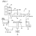
- Fig. 1 is a schematic depiction of a PECVD chamber for carrying out selected steps in the process of the present invention.
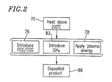
- Fig. 2 is a block diagram illustrating the steps in the process for depositing fluorinated amorphous carbon on a substrate in a PECVD chamber as shown in the Fig. 1, in accordance with the present invention.
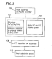
- Fig. 3 is a block diagram illustrating a preferred embodiment of a process for depositing fluorinated amorphous carbon on a substrate in a PECVD chamber, carrying the process through to a final anneal.
- the present invention provides a process for depositing fluorinated amorphous carbon (a-F:C) on a silicon wafer or other substrate.
- the wafer substrate at the time the steps in the method are carried out, has been processed by well-known techniques (not shown) to produce integrated circuit (IC) features (e.g., transistors and other active and passive devices) on the wafer.
- IC integrated circuit
- the type and number of integrated circuit features on the substrate are unimportant to the process of the present invention, except that the low-k fluorinated amorphous carbon dielectric material is most advantageously employed on ultra-large-scale-integration (ULSI) high-density ICs.
- ULSI ultra-large-scale-integration
- the dielectric material is used in interconnect structures, such as conductive lines and vias (not shown) which are well-known conductive interconnect features typically formed in, and extend through, the interconnect dielectric film which is deposited on the wafer, including the a-F:C dielectric deposited in the method of the present invention.
- interconnect structures such as conductive lines and vias (not shown) which are well-known conductive interconnect features typically formed in, and extend through, the interconnect dielectric film which is deposited on the wafer, including the a-F:C dielectric deposited in the method of the present invention.
- the form, architecture, and conductive materials used in the interconnect structures, as well as the methods of forming such structures, are not described herein and are a matter of design choice well known to those skilled in the art.
- This invention relates to the method of forming a suitable low-dielectric-constant (low-k) dielectric film which is deposited on the wafer and is suitable for use between and around the conductive lines, vias, and other conductors in ULSI and similar ICs.
- low-k dielectric film which is deposited on the wafer and is suitable for use between and around the conductive lines, vias, and other conductors in ULSI and similar ICs.
- Fig. 1 is a schematic illustration of a suitable apparatus 10 for carrying out a plasma enhanced chemical vapor deposition (PECVD) on a substrate such as wafer 12.
- Apparatus 10 includes a PECVD chamber 16 of a size suitable for holding one or more wafers 12, which are supported in the chamber on a chuck 20.
- the interior 22 can be evacuated or pressurized as desired by a suitable pump and valve apparatus schematically illustrated in Fig. 1 by pump 26.
- Individual wafers 12 are moved in and out of chamber 16 by a suitable wafer handler 30 through a gate valve 32 in the chamber wall, allowing wafers to be moved onto chuck 20 for processing, and then removed from the chamber.
- Selected gases used in PECVD processing are introduced into the chamber through a suitable manifold system 36 from various gas supply reservoirs indicated collectively at 40, controlled by valves 42.
- the gases are introduced into the chamber through what is called a shower head 46, which distributes the gases as required.
- Chuck 20 can be heated to any desired temperature, the heating element for this purpose being schematically depicted as heater 50.
- the heater and chuck are used to select the temperature of wafer 12 during PECVD processing.
- Plasma energy is supplied to the chamber through an RF generator 52 which supplies high frequency (HF) RF power radiated through shower head 46.
- HF high frequency
- Apparatus 10 preferably also includes a low frequency (LF) generator 56 for supplying LF power to the interior of the chamber.
- LF power is applied between the chuck 20 and shower head 46 in a manner well known to those skilled in the art.
- LF power is used to increase crosslinking in the amorphous fluorinated carbon (a-F:C) film deposited on wafer 12 during PECVD processing.
- Fig. 2 illustrates the steps in the process of the present invention, which will be described with reference to Figs. 1 and 2.
- a wafer substrate 12 is first positioned on chuck 20 in PECVD chamber 16 by wafer handler 30.
- the substrate 12 is typically a silicon wafer prepared for receiving a-F:C, the a-F:C being deposited on the upper surface 58 of the wafer.
- the first step shown in Fig. 2 is step 70, which is the heating of substrate 12 to a temperature above 200°C.
- wafer 12 is heated to a temperature generally in the range of 200°C-300°C.
- the next step 76 is the introduction of a flow of fluorine containing gas (FCG) and carbon containing gas (CCG) into chamber 16 via manifold 36 from suitable supplies 40.
- FCG fluorine containing gas
- CCG carbon containing gas
- the preferred FCG is octafluorocyclobutane (C 4 F 8 ) and the preferred CCG is methane (CH 4 ).
- the ratio of FCG/CCG introduced into chamber 16 is selected to deposit a-F:C on substrate 12 by plasma enhanced chemical vapor deposition. The suggested ratio is between 1/1 and 30/1 (FCG/CCG) and, preferably, between 5/1 and 15/1.
- suitable plasma power is applied in chamber 16 (step 78).
- suitable plasma power includes HF energy (13.56 MHz), at an energy level of between 0.5 Watts and 3.0 Watts per square centimeter of substrate surface (i.e., the surface area of substrate 12), and LF energy, at a frequency generally in the range of 100 KHz 900 KHz, at an energy level of 0.5 Watts and 3:0 Watts per square centimeter of substrate surface.
- C 4 F 8 provides discharge of two kinds of long-life radicals.
- One is the fluorocarbon radical (CF x ) (wherein 1 ⁇ x ⁇ 2 ), which is the building block for a-F:C deposits.
- the other is F and F 2 atoms, which are destructive etchants that form volatile fluorides which weaken the a-F:C film deposited on substrate 12.
- the methane serves to discharge hydrogen (H) radicals, which can tie up F atoms by forming volatile HF, which reduces the etching from the F and F 2 atoms, thus improving the stability of the resultant a-F:C film deposited on the wafer.
- the deposition rate and the fluorine concentration of the a-F:C film are selectively controlled by the flow rates of the FCG and CCG gases, as well as the chamber pressure within chamber 16.
- the ratio of FCG to CCG is generally between 1 to 1 and 30 to 1 and is preferably between 5 to 1 and 15 to 1 (FCG to CCG).
- the ambient pressure maintained within chamber 16 during steps 76 and 78 is preferably generally in the range of 0.3 Torr to 2.0 Torr.
- the present invention further includes the additional step 80 of introducing silane (SiH 4 ) gas into chamber 16, together with the FCG and CCG gases, during steps 76 and 78.
- the percentage of silane introduced into chamber 16 during step 80 is preferably generally in the range of 1% to 15% of the total introduced gases (i.e., FCG and CCG and silane).
- the silane has been found to improve the thermal stability of the deposited a-F:C film.
- Thermal stability is generally defined as minimal-to-zero shrinkage (e.g.. less than 1% shrinkage) of the deposited a-F:C film during the high temperature anneal which is carried out upon completion of the interlevel interconnects on an IC wafer. It is advantageous in IC wafer fabrication to be able to anneal the fabricated wafer at a temperature above 440°C for a minimum of approximately 20 minutes, and preferably between 30 minutes and up to several hours.
- the anneal is generally a part of the completion process for the devices on the wafer.
- One significant problem with the use of a-F:C dielectrics on IC wafers has been its poor thermal stability during anneals over 350°C-400°C.
- Fluorinated amorphous carbon films deposited using prior art processes, when subjected to higher temperature anneals (440°C+) exhibit undesirable shrinkage, for example, 5% - 20% or more.
- thermal stability minimum or zero shrinkage at final anneals up to 440°C - 465°C
- Fig. 3 shows an illustrative embodiment the process of the present invention, explaining the process in greater detail.
- the wafer 12 is positioned on chuck 20 in chamber 16 and heated to a temperature generally in the range of 200°C to 300°C.
- gases C 4 F 8 , CH 4 , and SiH 4 are introduced into chamber 16 via supplies 40 and valves 42 and manifold 36.
- the gases are distributed in chamber 16 through showerhead 46.
- the flow rates of gases during step 102 are the rates required to maintain the ambient pressure within chamber 16 generally in the range of 0.3 Torr and 2.0 Torr.
- the ratio of C 4 F 8 to CH 4 (C 4 F 8 /CH 4 ) during step 102 is generally in the range of 1/1 to 30/1 and preferably between 5/1 and 15/1.
- the percentage of silane gas introduced in step 102, as a percentage of the three introduced gases C 4 F 8 , CH 4 , and SiH 4 is generally in the range of 1% to 15% SiH 4 .
- the flow of C 4 F 8 , CH 4 , and SiH 4 during step 102 can alternatively be characterized as flow rates measured in standard cubic centimeters per minute (sccm), per cubic meter of interior volume 22 in PECVD chamber 16.
- sccm standard cubic centimeters per minute
- the following are suitable flow rates (per m 3 of chamber volume) for carrying out step 102:
- step 104 is carried out by applying HF and LF plasma energy in chamber 16.
- the HF energy is at a suggested standard frequency of 13.56 MHz and at an energy level of between 0.5 Watts and 3.0 Watts per square centimeter of surface area 58 of substrate wafer 12.
- LF energy is applied at a frequency generally in the range of 100 KHz to 900 KHz at an energy level of between 0.5 Watts and 3.0 Watts per square centimeter of substrate surface.
- Steps 102 and 104 deposit a-F:C on wafer 12 (step 108).
- a suitable thickness of a-F:C film deposited in step 108 is generally in the range of 1,000 angstroms to 10,000 angstroms.
- wafer 12 is removed from chamber 16 by any suitable means, such as handler 30, and annealed (step 110) in a suitable annealing oven at a temperature generally in the range of 300°C to 550°C.
- a suitable annealing oven at a temperature generally in the range of 300°C to 550°C.
- the process exhibits good thermal stability (i.e., shrinkage of less than approximately 1%) at anneal temperatures above 440°C, generally in the range of 440°C - 465°C.
- a 6-inch wafer 12 was placed on chuck 20 and heated to a temperature of 250°C.
- a flow of C 4 F 8 , CH 4 , and SiH 4 gases was introduced into the chamber at the following flow rates
- HF power 13.56 MHz was applied at a power level of 200 Watts and LF power (500 KHz) was applied at 200 Watts.
- the ambient pressure in the chamber was maintained at approximately 0.4 Torr.
- the above conditions produced a deposition rate of a-F:C of 1,200 angstroms/minute. Deposition was carried out for four minutes. Then the wafer was removed from the chamber and a final anneal was carried out at 450° C for 30 minutes.
- the resultant dielectric constant k of the a-F:C was approximately 2.3.
- the present invention has been found to improve the thermal stability and lower the dielectric constant of deposited a-F:C films formed by PECVD processes. Variations in the process are possible within the scope of the present inventions For example, the deposition temperature and ratio of gases specified in the experimental example are suggestive only. Within the specified ranges disclosed herein, it will be necessary to optimize the flow rates and temperatures used in IC manufacturing processes which are employed for commercial production.
Abstract
Description
| Relevant properties for several members of carbon family | ||||
| Material | Chemical Composition | Structure | k | Thermal Stability |
| Diamond | C | Crystalline, fully crosslinked | Greater than 5 | Very high |
| Hydrogenated Carbon (a-H:C) or Diamondlike Carbon (DLC) | C & H H: 30 at. % - 50 at.% | Amorphous polymer, highly crosslinked | 2.7 - 3.8 | 350 - 400 °C |
| Fluorinated Amorphous Carbon (a-F:C) | C & F F: 40 at.% - 50 at.% | Amorphous polymer, highly crosslinked | 2.1 - 2.8 | 300 - 420 °C |
| PTFE or Teflon | C & F F: 67 at.% | (- CF2 -) polymer, uncrosslinked | 2.0 | < 300 °C |
- Precursor: C4F8 + CH4
- Free radicals produced by plasma discharge:
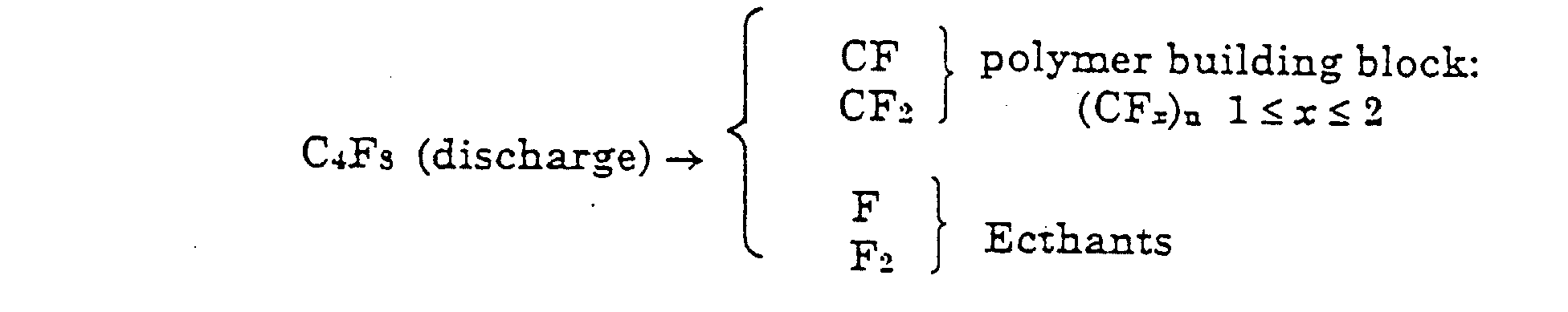
- Adding CH4 → suppressing fluorine etching to (CFx)n deposits:

- Adding SiH4 → suppressing fluorine etching to (CFx)n deposits:

Claims (21)
- A plasma enhanced chemical vapor deposition (PECVD) process for depositing a dielectric material on a substrate for use in interconnect structures of integrated circuits, the method comprising the following steps:a) position the substrate in a PECVD chamber and heat the substrate to a temperature above 200°C;b) introduce a flow of fluorine containing gas (FCG) and carbon containing gas (CCG) into the chamber under sufficient applied energy to form a fluorine and carbon gas plasma, the ratio FCG to CCG being selected to deposit fluorinated amorphous carbon on the substrate; andc) introduce a flow of SiH4 (silane) into the chamber together with the FCG and CCG in step b), whereby the silane increases the thermal stability of the fluorinated amorphous carbon deposited on the substrate.
- A PECVD process as in claim 1 in which the substrate is heated to a temperature generally in the range of 200°C to 300°C in step a),
- A PECVD process as in claim 1 in which the FCG introduced in step b) is C4F8.
- A PECVD process as in claim 3 in which the CCG introduced in step b) is CH4.
- A PECVD process as in claim 4 in which the ambient pressure in the PECVD chamber maintained during the introduction of C4F8, CH4, and silane is generally in the range of 0.3 Torr to 2.0 Torr.
- A PECVD process as in claim 5 in which the ratio of C4F8 to CH4 (C4F8/CH4) introduced into the PECVD chamber during steps b) and c) is generally between 1/1 and 30/1.
- A PECVD process as in claim 5 in which the ratio of C4F8 to CH4 (C4F8/CH4) introduced into the PECVD chamber during steps b) and c) is generally between 5/1 and 15/1.
- A PECVD process as in claim 6 in which the percentage of silane in the C4F8, CH4, and silane gases introduced into the PECVD chamber in steps b) and c) is generally in the range of 1% to 15%.
- A PECVD process as in claim 5 in which flow rates of the C4F8, CH4, and silane gases introduced into the PECVD chamber in steps b) and c), per cm3 of the chamber interior volume, are generally in the following ranges:3000 to 10,000 sccm of C4F8 per m3;300 to 1100 sccm CH4 per m3; and100 to 550 sccm of silane per m3.
- A PECVD process as in claim 1 in which the plasma energy applied in the chamber to form the gas plasma therein includes high-frequency energy at a frequency of 13.56 MHz and an energy level of between 0.5 Watts and 3.0 Watts per square centimeter of substrate surface.
- A PECVD process as in claim 10 in which the plasma energy applied in the chamber further includes low-frequency energy at a frequency generally in the range of 100 KHz to 900KHz and energy level of between 0.5 Watts and 3.0 Watts per square centimeter of substrate surface.
- A PECVD process as in claim 1 including continuing the process until a selected thickness of fluorinated amorphous carbon is deposited on the substrate, and further including the step of annealing the substrate at a temperature generally in the range of 300°C to 550°C.
- A plasma enhanced chemical vapor deposition (PECVD) process for depositing fluorinated amorphous carbon dielectric on a substrate for use in interconnect structures of integrated circuits, the method comprising the following steps:a) position the substrate in a PECVD chamber and heat the substrate to a temperature between 200°C and 300°C;b) introduce octafluorocyclobutane (C4F8), methane (CH4), and silane (SiH4) into the chamber, wherein the percentage of silane in the introduced gases is generally in the range of 1% to 15%;c) apply plasma energy in the chamber to form a gas plasma which includes CFx polymer radicals, wherein x is greater than or equal to 1 and less than or equal to 2, for depositing fluorinated amorphous carbon on the substrate; andd) maintain a sufficient flow of octafluorocyclobutane, methane, and silane into the chamber during step b) to provide an interior chamber pressure generally in the range of 0.3 Torr to 2.0 Torr until a selected thickness of fluorinated amorphous carbon is deposited on the substrate.
- A PECVD process as in claim 13 in which the plasma energy applied in the chamber further includes high-frequency energy at a frequency of 13.56 MHz and an energy level of between 0.5 Watts and 3.0 Watts per square centimeter of substrate surface.
- A PECVD process as in claim 14 in which the plasma energy applied in the chamber further includes low-frequency energy at a frequency generally in the range of 100 KHz to 900 KHz and energy level of between 0.5 Watts and 3.0 Watts per square centimeter of substrate surface.
- A PECVD process as in claim 13 in which the ratio of octafluorocyclobutane to methane (C4F8/CH4) introduced into the PECVD chamber during the process is generally between 1/1 and 30/1.
- A PECVD process as in claim 16 in which the percentage of silane in the C4F8, CH4, and silane gases introduced into the PECVD chamber in steps b) and c) is generally in the range of 1% to 15%.
- A PECVD process as in claim 13 in which the ratio of octafluorocyclobutane to methane (C4F8/CH4) introduced into the PECVD chamber during the process is generally between 5/1 and 15/1.
- A PECVD process as in claim 18 in which the percentage of silane in the C4F8, CH4, and silane gases introduced into the PECVD chamber in steps b) and c) is generally in the range of 1% to 15%.
- A PECVD process as in claim 13 including continuing the process until a selected thickness of fluorinated amorphous carbon is deposited on the substrate, and further including the step of annealing the substrate at a temperature greater than or equal to 440°C.
- A process for depositing a fluorinated amorphous carbon (a-F:C) film on a substrate using a plasma enhanced chemical vapour deposition (PECVD) method carried out in an atmosphere comprising C4F8 and CH4, characterised by the introduction of silane gas (SiH4) into the PECVD chamber in which the method is performed.
Applications Claiming Priority (2)
| Application Number | Priority Date | Filing Date | Title |
|---|---|---|---|
| US23382 | 1998-02-13 | ||
| US09/023,382 US5900290A (en) | 1998-02-13 | 1998-02-13 | Method of making low-k fluorinated amorphous carbon dielectric |
Publications (3)
| Publication Number | Publication Date |
|---|---|
| EP0936282A2 true EP0936282A2 (en) | 1999-08-18 |
| EP0936282A3 EP0936282A3 (en) | 2001-06-27 |
| EP0936282B1 EP0936282B1 (en) | 2006-10-18 |
Family
ID=21814764
Family Applications (1)
| Application Number | Title | Priority Date | Filing Date |
|---|---|---|---|
| EP99300444A Expired - Lifetime EP0936282B1 (en) | 1998-02-13 | 1999-01-21 | Low-k fluorinated amorphous carbon dielectric and method of making the same |
Country Status (6)
| Country | Link |
|---|---|
| US (1) | US5900290A (en) |
| EP (1) | EP0936282B1 (en) |
| JP (1) | JPH11251308A (en) |
| KR (1) | KR100283007B1 (en) |
| DE (1) | DE69933598T2 (en) |
| TW (1) | TW414812B (en) |
Families Citing this family (34)
| Publication number | Priority date | Publication date | Assignee | Title |
|---|---|---|---|---|
| US5989998A (en) * | 1996-08-29 | 1999-11-23 | Matsushita Electric Industrial Co., Ltd. | Method of forming interlayer insulating film |
| EP1033746A4 (en) * | 1997-11-20 | 2003-05-28 | Tokyo Electron Ltd | Method of forming film by plasma |
| JP3429171B2 (en) * | 1997-11-20 | 2003-07-22 | 東京エレクトロン株式会社 | Plasma processing method and semiconductor device manufacturing method |
| JP3574734B2 (en) * | 1997-11-27 | 2004-10-06 | 東京エレクトロン株式会社 | Method for manufacturing semiconductor device |
| US6147407A (en) * | 1998-03-27 | 2000-11-14 | Lucent Technologies Inc. | Article comprising fluorinated amorphous carbon and process for fabricating article |
| US6184157B1 (en) * | 1998-06-01 | 2001-02-06 | Sharp Laboratories Of America, Inc. | Stress-loaded film and method for same |
| SG81991A1 (en) * | 1999-05-25 | 2001-07-24 | Tokyo Electron Ltd | Method for producing insulator film |
| KR100436829B1 (en) * | 1999-06-18 | 2004-06-23 | 닛신덴키 가부시키 가이샤 | Carbon film and method for formation thereof and article covered with carbon film and method for preparation thereof |
| ATE418158T1 (en) * | 1999-08-17 | 2009-01-15 | Applied Materials Inc | SURFACE TREATMENT OF CARBON-DOPED SIO2 FILM TO INCREASE STABILITY DURING O2 ASHING |
| US6602806B1 (en) | 1999-08-17 | 2003-08-05 | Applied Materials, Inc. | Thermal CVD process for depositing a low dielectric constant carbon-doped silicon oxide film |
| KR100541541B1 (en) * | 1999-08-26 | 2006-01-12 | 삼성전자주식회사 | Process Chamber of Plasma Process System |
| JP4140674B2 (en) | 1999-09-27 | 2008-08-27 | 東京エレクトロン株式会社 | Method and apparatus for observing porous amorphous film |
| US6296906B1 (en) | 1999-09-30 | 2001-10-02 | Novellus Systems, Inc. | Annealing process for low-k dielectric film |
| US6303518B1 (en) | 1999-09-30 | 2001-10-16 | Novellus Systems, Inc. | Methods to improve chemical vapor deposited fluorosilicate glass (FSG) film adhesion to metal barrier or etch stop/diffusion barrier layers |
| US6572937B2 (en) * | 1999-11-30 | 2003-06-03 | The Regents Of The University Of California | Method for producing fluorinated diamond-like carbon films |
| US20020005539A1 (en) * | 2000-04-04 | 2002-01-17 | John Whitman | Spin coating for maximum fill characteristic yielding a planarized thin film surface |
| US6458718B1 (en) | 2000-04-28 | 2002-10-01 | Asm Japan K.K. | Fluorine-containing materials and processes |
| US6486078B1 (en) | 2000-08-22 | 2002-11-26 | Advanced Micro Devices, Inc. | Super critical drying of low k materials |
| US6632478B2 (en) | 2001-02-22 | 2003-10-14 | Applied Materials, Inc. | Process for forming a low dielectric constant carbon-containing film |
| WO2002081546A1 (en) * | 2001-04-06 | 2002-10-17 | Honeywell International Inc. | Low dielectric constant materials and methods of preparation thereof |
| JP4758938B2 (en) * | 2001-08-30 | 2011-08-31 | 東京エレクトロン株式会社 | Insulating film forming method and insulating film forming apparatus |
| US20040247896A1 (en) * | 2001-12-31 | 2004-12-09 | Paul Apen | Organic compositions |
| WO2004051708A2 (en) * | 2002-11-29 | 2004-06-17 | Fraunhofer-Gesellschaft zur Förderung der angewandten Forschung e.V. | Method and device for machining a wafer, in addition to a wafer comprising a separation layer and a support layer |
| US20060166491A1 (en) * | 2005-01-21 | 2006-07-27 | Kensaku Ida | Dual damascene interconnection having low k layer and cap layer formed in a common PECVD process |
| DE102005034764B4 (en) * | 2005-07-26 | 2012-08-02 | Fraunhofer-Gesellschaft zur Förderung der angewandten Forschung e.V. | Process for the preparation of functional fluorocarbon polymer layers by plasma polymerization of perfluorocycloalkanes and substrates coated therewith |
| US8206996B2 (en) * | 2006-03-28 | 2012-06-26 | Lam Research Corporation | Etch tool process indicator method and apparatus |
| US7951616B2 (en) * | 2006-03-28 | 2011-05-31 | Lam Research Corporation | Process for wafer temperature verification in etch tools |
| KR101669470B1 (en) | 2009-10-14 | 2016-10-26 | 삼성전자주식회사 | Semiconductor device including metal silicide layer |
| US9520372B1 (en) | 2015-07-20 | 2016-12-13 | Taiwan Semiconductor Manufacturing Company, Ltd. | Wafer level package (WLP) and method for forming the same |
| WO2018191484A1 (en) * | 2017-04-13 | 2018-10-18 | Applied Materials, Inc. | Method and apparatus for deposition of low-k films |
| KR20230169654A (en) * | 2022-06-09 | 2023-12-18 | 충남대학교산학협력단 | High-k Amorphous Fluorinated Carbon Thin Films, Preparation Method thereof and Applications to Semiconductor or Capacitor Devices |
| KR20240037609A (en) | 2022-09-15 | 2024-03-22 | 충남대학교산학협력단 | Semiconductor Structure and Semiconductor Devices Comprising High-k Amorphous Fluorinated Carbon Ultrathin Film Layer and Preparation Method thereof |
| KR20240037610A (en) | 2022-09-15 | 2024-03-22 | 충남대학교산학협력단 | Semiconductor Devices Comprising High-k Amorphous Fluorinated Carbon Thin Film as Gate Dielectric layer and Preparation Method thereof |
| KR20240037612A (en) | 2022-09-15 | 2024-03-22 | 충남대학교산학협력단 | Semiconductor Structure and Semiconductor Devices Comprising High-k Amorphous Fluorinated Carbon Ultrathin Film Layer and Preparation Method thereof |
Citations (3)
| Publication number | Priority date | Publication date | Assignee | Title |
|---|---|---|---|---|
| EP0454456A1 (en) * | 1990-04-26 | 1991-10-30 | Canon Kabushiki Kaisha | Light receiving member with an amorphous silicon photoconductive layer containing fluorine atoms in an amount of 1 to 95 atomic ppm |
| EP0701283A2 (en) * | 1994-09-12 | 1996-03-13 | Nec Corporation | Semiconductor device with amorphous carbon layer and method of fabricating the same |
| EP0768388A2 (en) * | 1995-10-12 | 1997-04-16 | Nec Corporation | Method and apparatus for forming amorphous carbon film |
Family Cites Families (1)
| Publication number | Priority date | Publication date | Assignee | Title |
|---|---|---|---|---|
| JPS62180073A (en) * | 1986-02-03 | 1987-08-07 | Ricoh Co Ltd | Amorphous carbon film and its production |
-
1998
- 1998-02-13 US US09/023,382 patent/US5900290A/en not_active Expired - Fee Related
- 1998-11-27 JP JP10338211A patent/JPH11251308A/en active Pending
- 1998-12-08 TW TW087120344A patent/TW414812B/en not_active IP Right Cessation
-
1999
- 1999-01-21 DE DE69933598T patent/DE69933598T2/en not_active Expired - Fee Related
- 1999-01-21 EP EP99300444A patent/EP0936282B1/en not_active Expired - Lifetime
- 1999-02-03 KR KR1019990003534A patent/KR100283007B1/en not_active IP Right Cessation
Patent Citations (3)
| Publication number | Priority date | Publication date | Assignee | Title |
|---|---|---|---|---|
| EP0454456A1 (en) * | 1990-04-26 | 1991-10-30 | Canon Kabushiki Kaisha | Light receiving member with an amorphous silicon photoconductive layer containing fluorine atoms in an amount of 1 to 95 atomic ppm |
| EP0701283A2 (en) * | 1994-09-12 | 1996-03-13 | Nec Corporation | Semiconductor device with amorphous carbon layer and method of fabricating the same |
| EP0768388A2 (en) * | 1995-10-12 | 1997-04-16 | Nec Corporation | Method and apparatus for forming amorphous carbon film |
Non-Patent Citations (1)
| Title |
|---|
| YANG H ET AL: "DEPOSITION OF HIGHLY CROSSLINKED FLUORINATED AMORPHOUS CARBON FILM AND STRUCTURAL EVOLUTION DURING THERMAL ANNEALING" APPLIED PHYSICS LETTERS,AMERICAN INSTITUTE OF PHYSICS. NEW YORK,US, vol. 73, no. 11, 14 September 1998 (1998-09-14), pages 1514-1516, XP000784064 ISSN: 0003-6951 * |
Also Published As
| Publication number | Publication date |
|---|---|
| KR100283007B1 (en) | 2001-02-15 |
| DE69933598D1 (en) | 2006-11-30 |
| TW414812B (en) | 2000-12-11 |
| US5900290A (en) | 1999-05-04 |
| EP0936282B1 (en) | 2006-10-18 |
| EP0936282A3 (en) | 2001-06-27 |
| JPH11251308A (en) | 1999-09-17 |
| KR19990072395A (en) | 1999-09-27 |
| DE69933598T2 (en) | 2007-08-23 |
Similar Documents
| Publication | Publication Date | Title |
|---|---|---|
| EP0936282B1 (en) | Low-k fluorinated amorphous carbon dielectric and method of making the same | |
| US6440878B1 (en) | Method to enhance the adhesion of silicon nitride to low-k fluorinated amorphous carbon using a silicon carbide adhesion promoter layer | |
| US6410462B1 (en) | Method of making low-K carbon doped silicon oxide | |
| US6991959B2 (en) | Method of manufacturing silicon carbide film | |
| US6919270B2 (en) | Method of manufacturing silicon carbide film | |
| US6593655B1 (en) | Method for producing hydrogenated silicon oxycarbide films having low dielectric constant | |
| US5869149A (en) | Method for preparing nitrogen surface treated fluorine doped silicon dioxide films | |
| JP4272424B2 (en) | Ultralow dielectric constant material as an in-level or inter-level dielectric of a semiconductor element, method for manufacturing the same, and electronic device including the same | |
| US6632478B2 (en) | Process for forming a low dielectric constant carbon-containing film | |
| US7030468B2 (en) | Low k and ultra low k SiCOH dielectric films and methods to form the same | |
| US6448186B1 (en) | Method and apparatus for use of hydrogen and silanes in plasma | |
| US6184572B1 (en) | Interlevel dielectric stack containing plasma deposited fluorinated amorphous carbon films for semiconductor devices | |
| EP0934433B1 (en) | Method for depositing fluorine doped silicon dioxide films | |
| KR20010075563A (en) | Silicon carbide deposition method and use as a barrier layer and passivation layer | |
| US6790789B2 (en) | Ultralow dielectric constant material as an intralevel or interlevel dielectric in a semiconductor device and electronic device made | |
| EP1217648A2 (en) | Method of manufacturing an interlayer dielectric layer with low dielectric constant | |
| US20050048795A1 (en) | Method for ultra low-K dielectric deposition | |
| US6419985B1 (en) | Method for producing insulator film | |
| US6303519B1 (en) | Method of making low K fluorinated silicon oxide | |
| US6541400B1 (en) | Process for CVD deposition of fluorinated silicon glass layer on semiconductor wafer | |
| KR20050083787A (en) | Semiconductor device and process for producing the same | |
| US6844612B1 (en) | Low dielectric constant fluorine-doped silica glass film for use in integrated circuit chips and method of forming the same | |
| KR20210082265A (en) | 1-Methyl-1-iso-propoxy-silacycloalkane and high-density organosilica film prepared therefrom |
Legal Events
| Date | Code | Title | Description |
|---|---|---|---|
| PUAI | Public reference made under article 153(3) epc to a published international application that has entered the european phase |
Free format text: ORIGINAL CODE: 0009012 |
|
| AK | Designated contracting states |
Kind code of ref document: A2 Designated state(s): DE FR GB |
|
| AX | Request for extension of the european patent |
Free format text: AL;LT;LV;MK;RO;SI |
|
| PUAL | Search report despatched |
Free format text: ORIGINAL CODE: 0009013 |
|
| AK | Designated contracting states |
Kind code of ref document: A3 Designated state(s): AT BE CH CY DE DK ES FI FR GB GR IE IT LI LU MC NL PT SE |
|
| AX | Request for extension of the european patent |
Free format text: AL;LT;LV;MK;RO;SI |
|
| 17P | Request for examination filed |
Effective date: 20011212 |
|
| AKX | Designation fees paid |
Free format text: DE FR GB |
|
| 17Q | First examination report despatched |
Effective date: 20050704 |
|
| GRAP | Despatch of communication of intention to grant a patent |
Free format text: ORIGINAL CODE: EPIDOSNIGR1 |
|
| GRAS | Grant fee paid |
Free format text: ORIGINAL CODE: EPIDOSNIGR3 |
|
| GRAA | (expected) grant |
Free format text: ORIGINAL CODE: 0009210 |
|
| AK | Designated contracting states |
Kind code of ref document: B1 Designated state(s): DE FR GB |
|
| REG | Reference to a national code |
Ref country code: GB Ref legal event code: FG4D |
|
| REF | Corresponds to: |
Ref document number: 69933598 Country of ref document: DE Date of ref document: 20061130 Kind code of ref document: P |
|
| ET | Fr: translation filed | ||
| PLBE | No opposition filed within time limit |
Free format text: ORIGINAL CODE: 0009261 |
|
| STAA | Information on the status of an ep patent application or granted ep patent |
Free format text: STATUS: NO OPPOSITION FILED WITHIN TIME LIMIT |
|
| 26N | No opposition filed |
Effective date: 20070719 |
|
| PGFP | Annual fee paid to national office [announced via postgrant information from national office to epo] |
Ref country code: DE Payment date: 20090115 Year of fee payment: 11 |
|
| PGFP | Annual fee paid to national office [announced via postgrant information from national office to epo] |
Ref country code: GB Payment date: 20090121 Year of fee payment: 11 |
|
| PGFP | Annual fee paid to national office [announced via postgrant information from national office to epo] |
Ref country code: FR Payment date: 20090113 Year of fee payment: 11 |
|
| GBPC | Gb: european patent ceased through non-payment of renewal fee |
Effective date: 20100121 |
|
| REG | Reference to a national code |
Ref country code: FR Ref legal event code: ST Effective date: 20100930 |
|
| PG25 | Lapsed in a contracting state [announced via postgrant information from national office to epo] |
Ref country code: FR Free format text: LAPSE BECAUSE OF NON-PAYMENT OF DUE FEES Effective date: 20100201 |
|
| PG25 | Lapsed in a contracting state [announced via postgrant information from national office to epo] |
Ref country code: DE Free format text: LAPSE BECAUSE OF NON-PAYMENT OF DUE FEES Effective date: 20100803 |
|
| PG25 | Lapsed in a contracting state [announced via postgrant information from national office to epo] |
Ref country code: GB Free format text: LAPSE BECAUSE OF NON-PAYMENT OF DUE FEES Effective date: 20100121 |