EP0940889A2 - Method of mounting an electrical receptacle on a substrate - Google Patents
Method of mounting an electrical receptacle on a substrate Download PDFInfo
- Publication number
- EP0940889A2 EP0940889A2 EP99301367A EP99301367A EP0940889A2 EP 0940889 A2 EP0940889 A2 EP 0940889A2 EP 99301367 A EP99301367 A EP 99301367A EP 99301367 A EP99301367 A EP 99301367A EP 0940889 A2 EP0940889 A2 EP 0940889A2
- Authority
- EP
- European Patent Office
- Prior art keywords
- receptacle
- electrical
- substrate
- mounting
- circuit board
- Prior art date
- Legal status (The legal status is an assumption and is not a legal conclusion. Google has not performed a legal analysis and makes no representation as to the accuracy of the status listed.)
- Granted
Links
- 239000000758 substrate Substances 0.000 title claims abstract description 64
- 238000000034 method Methods 0.000 title claims abstract description 48
- 238000005476 soldering Methods 0.000 claims abstract description 32
- 238000010008 shearing Methods 0.000 claims abstract description 4
- 229910000679 solder Inorganic materials 0.000 claims description 17
- 239000012777 electrically insulating material Substances 0.000 claims description 14
- 230000004907 flux Effects 0.000 claims description 6
- 238000005406 washing Methods 0.000 claims description 4
- 238000010438 heat treatment Methods 0.000 claims description 3
- 239000004020 conductor Substances 0.000 description 43
- 239000011810 insulating material Substances 0.000 description 21
- 241000234295 Musa Species 0.000 description 19
- 235000018290 Musa x paradisiaca Nutrition 0.000 description 19
- PXHVJJICTQNCMI-UHFFFAOYSA-N Nickel Chemical compound [Ni] PXHVJJICTQNCMI-UHFFFAOYSA-N 0.000 description 8
- 238000013461 design Methods 0.000 description 7
- 239000000463 material Substances 0.000 description 6
- 238000004519 manufacturing process Methods 0.000 description 5
- 238000007747 plating Methods 0.000 description 5
- 238000005452 bending Methods 0.000 description 4
- 229910052759 nickel Inorganic materials 0.000 description 4
- 238000001746 injection moulding Methods 0.000 description 3
- 238000003780 insertion Methods 0.000 description 3
- 230000037431 insertion Effects 0.000 description 3
- 229910001369 Brass Inorganic materials 0.000 description 2
- 239000004677 Nylon Substances 0.000 description 2
- 238000004026 adhesive bonding Methods 0.000 description 2
- 239000010951 brass Substances 0.000 description 2
- 238000005259 measurement Methods 0.000 description 2
- 229920001778 nylon Polymers 0.000 description 2
- 239000000523 sample Substances 0.000 description 2
- 238000012360 testing method Methods 0.000 description 2
- 238000003466 welding Methods 0.000 description 2
- 239000000853 adhesive Substances 0.000 description 1
- 230000001070 adhesive effect Effects 0.000 description 1
- 230000008878 coupling Effects 0.000 description 1
- 238000010168 coupling process Methods 0.000 description 1
- 238000005859 coupling reaction Methods 0.000 description 1
- 238000000151 deposition Methods 0.000 description 1
- 238000007772 electroless plating Methods 0.000 description 1
- 238000009713 electroplating Methods 0.000 description 1
- PCHJSUWPFVWCPO-UHFFFAOYSA-N gold Chemical compound [Au] PCHJSUWPFVWCPO-UHFFFAOYSA-N 0.000 description 1
- 229910052737 gold Inorganic materials 0.000 description 1
- 239000010931 gold Substances 0.000 description 1
- 231100001261 hazardous Toxicity 0.000 description 1
- 238000009413 insulation Methods 0.000 description 1
- 239000007788 liquid Substances 0.000 description 1
- 230000013011 mating Effects 0.000 description 1
- 229920000642 polymer Polymers 0.000 description 1
- 230000000750 progressive effect Effects 0.000 description 1
- 238000000926 separation method Methods 0.000 description 1
- 230000035939 shock Effects 0.000 description 1
- 229910052709 silver Inorganic materials 0.000 description 1
- 239000004332 silver Substances 0.000 description 1
- 239000000243 solution Substances 0.000 description 1
- 239000000126 substance Substances 0.000 description 1
Images


Classifications
-
- H—ELECTRICITY
- H01—ELECTRIC ELEMENTS
- H01R—ELECTRICALLY-CONDUCTIVE CONNECTIONS; STRUCTURAL ASSOCIATIONS OF A PLURALITY OF MUTUALLY-INSULATED ELECTRICAL CONNECTING ELEMENTS; COUPLING DEVICES; CURRENT COLLECTORS
- H01R24/00—Two-part coupling devices, or either of their cooperating parts, characterised by their overall structure
- H01R24/20—Coupling parts carrying sockets, clips or analogous contacts and secured only to wire or cable
-
- H—ELECTRICITY
- H01—ELECTRIC ELEMENTS
- H01R—ELECTRICALLY-CONDUCTIVE CONNECTIONS; STRUCTURAL ASSOCIATIONS OF A PLURALITY OF MUTUALLY-INSULATED ELECTRICAL CONNECTING ELEMENTS; COUPLING DEVICES; CURRENT COLLECTORS
- H01R12/00—Structural associations of a plurality of mutually-insulated electrical connecting elements, specially adapted for printed circuits, e.g. printed circuit boards [PCB], flat or ribbon cables, or like generally planar structures, e.g. terminal strips, terminal blocks; Coupling devices specially adapted for printed circuits, flat or ribbon cables, or like generally planar structures; Terminals specially adapted for contact with, or insertion into, printed circuits, flat or ribbon cables, or like generally planar structures
- H01R12/70—Coupling devices
- H01R12/7005—Guiding, mounting, polarizing or locking means; Extractors
- H01R12/7011—Locking or fixing a connector to a PCB
- H01R12/7064—Press fitting
-
- H—ELECTRICITY
- H01—ELECTRIC ELEMENTS
- H01R—ELECTRICALLY-CONDUCTIVE CONNECTIONS; STRUCTURAL ASSOCIATIONS OF A PLURALITY OF MUTUALLY-INSULATED ELECTRICAL CONNECTING ELEMENTS; COUPLING DEVICES; CURRENT COLLECTORS
- H01R2101/00—One pole
-
- Y—GENERAL TAGGING OF NEW TECHNOLOGICAL DEVELOPMENTS; GENERAL TAGGING OF CROSS-SECTIONAL TECHNOLOGIES SPANNING OVER SEVERAL SECTIONS OF THE IPC; TECHNICAL SUBJECTS COVERED BY FORMER USPC CROSS-REFERENCE ART COLLECTIONS [XRACs] AND DIGESTS
- Y10—TECHNICAL SUBJECTS COVERED BY FORMER USPC
- Y10T—TECHNICAL SUBJECTS COVERED BY FORMER US CLASSIFICATION
- Y10T29/00—Metal working
- Y10T29/49—Method of mechanical manufacture
- Y10T29/49002—Electrical device making
- Y10T29/49117—Conductor or circuit manufacturing
- Y10T29/49124—On flat or curved insulated base, e.g., printed circuit, etc.
- Y10T29/49147—Assembling terminal to base
- Y10T29/49149—Assembling terminal to base by metal fusion bonding
-
- Y—GENERAL TAGGING OF NEW TECHNOLOGICAL DEVELOPMENTS; GENERAL TAGGING OF CROSS-SECTIONAL TECHNOLOGIES SPANNING OVER SEVERAL SECTIONS OF THE IPC; TECHNICAL SUBJECTS COVERED BY FORMER USPC CROSS-REFERENCE ART COLLECTIONS [XRACs] AND DIGESTS
- Y10—TECHNICAL SUBJECTS COVERED BY FORMER USPC
- Y10T—TECHNICAL SUBJECTS COVERED BY FORMER US CLASSIFICATION
- Y10T29/00—Metal working
- Y10T29/49—Method of mechanical manufacture
- Y10T29/49002—Electrical device making
- Y10T29/49117—Conductor or circuit manufacturing
- Y10T29/49124—On flat or curved insulated base, e.g., printed circuit, etc.
- Y10T29/49147—Assembling terminal to base
- Y10T29/49151—Assembling terminal to base by deforming or shaping
- Y10T29/49153—Assembling terminal to base by deforming or shaping with shaping or forcing terminal into base aperture
Definitions
- the present invention relates generally to mounting an electrical receptacle on a substrate and more particularly to mounting a banana type receptacle to a circuit board for use in electronic instruments, such as power supplies, hand-held multimeters, oscilloscopes, time domain reflectometers, and the like.
- Banana type leads are used in the electronic industry for coupling signals to and from a device under test.
- a typical banana lead has a single wire terminated at each end with a male banana plug.
- the banana plug has an elongated conductive probe portion wrapped with a barrel spring, so that the probe portion may be inserted into a banana receptacle in an instrument.
- the banana receptacle has a conductive sleeve that makes contact with the barrel spring and is surrounded by electrically insulating material on the bottom and outer surface of the conductive sleeve.
- UL Underwriters Laboratories, UL, has established insulation standards for electronic measuring and testing equipment (UL1244) that establishes minimum distances between conductive elements and users for preventing hazardous electrical shocks.
- Banana type leads that meet this standard have a tubular shaped shroud enclosing the male banana plug.
- the shroud is a thin walled cylinder of insulating material that provides the minimum distance separation between the male plug, coaxially disposed within the shroud, and the user.
- the corresponding banana receptacle may include an outer ring of insulating material defining an annular bore coaxial with the insulated conductive sleeve. The shroud of the male plug fits into the annular ring of the receptacle with the male plug making electrical contact with the conductive sleeve.
- the conductive sleeve of the banana receptacle generally has electrical leads extending from the sleeve that are exposed at the bottom of the receptacle.
- the electrical leads are of a length that allows them to be inserted into electrically conductive apertures in a substrate, such as a circuit board. Conductive runs formed on the substrate couple the conductive apertures, and thus the conductive sleeve, to additional circuitry on the substrate.
- a particular problem with this type of banana receptacle is that the receptacle defines and controls the position of the circuit board in any hand-held electronic instrument design, and thus the overall design of the instrument.
- the height of the receptacle defines the minimum thickness for the instrument for at least that portion of the instrument where the receptacle is positioned.
- a more complex shell design having differing surface levels is required if the instruments thickness is to be less than the minimum thickness associated with the receptacle.
- a flat surface shell is chosen, then the internal circuitry design may become more complex and expensive.
- a custom display having a thickness matching the height of the receptacle may be required if the display is to be mounted directly onto the circuit board.
- conductive contact elements or cabling would be required for connecting the display to the circuit board which adds cost to the instrument.
- buttons and knobs associated with most hand-held electronic instruments would be affected by the circuit board positioning problem.
- An alternative to the above described receptacle-circuit board positioning problem is to remove the receptacles from the main circuit board.
- the receptacle or receptacles may be individually connected to the main circuit board via soldered wire connections between the receptacle leads and the circuit board.
- the receptacle or receptacles may also be bolted to the circuit board or instument case with wire leads connecting the receptacle to the circuit board.
- the receptacle or receptacles may further be placed on a separate circuit board and electrically connected to the main circuit board via soldered wire connections between the leads of the receptacle(s) and the main circuit board or providing some form of interconnect between the boards. While this solution frees designers from the receptacle-circuit board positioning problem, it adds component and manufacturing costs to the instrument.
- the mounting method should not add component or manufacturing costs to the instrument and should be compatible with automated circuit board manufacturing processes.
- the method should further be flexible to allow for positioning the electrical receptacle at any height within the circuit board. Additionally, the method should also be flexible for permitting the positioning of the circuit board containing the electrical receptacle anywhere within the shell of the instrument.
- an electronic measurement instrument such as a hand-held digital multimeter, time domain reflectometer, oscilloscope, or the like.
- the method of mounting an electrical receptacle on the substrate includes the steps of placing the electrical receptacle over an aperture formed in the substrate with the receptacle having a body of electrically insulating material partially surrounding an electrically conductive element having a deformable electrical lead with the body of electrically insulating material having support ribs formed on an exterior surface of the insulating body supporting the receptacle over the aperture and the electrical lead making an electrical connection with an electrical contact on the substrate.
- the electrical lead is affixed to the electrical contact and the receptacle is inserted into the substrate.
- the affixing step further includes the step of soldering wherein the preferred embodiment of the soldering step further includes the step of wave soldering.
- the wave soldering step further includes the steps of applying a solder flux to the substrate and heating the substrate prior to the soldering step.
- the inserting step further includes the step of deforming the electrical lead as the receptacle is inserted into the aperture.
- the inserting step further includes the steps of shearing or deforming the support ribs and positioning shoulders of alignment ribs, formed on the exterior surface of insulating body, against the substrate.
- the inserting step may further include the steps of deforming the support ribs and positioning shoulders of alignment ribs, formed on the exterior surface of the insulating body, against the substrate.
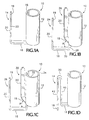
- Figs. 1A - 1D are perspective views of four embodiments of an electrically conductive element usable in an electrical receptacle used in the method of mounting an electrical receptacle on a substrate according to the present invention.
- Figs. 2A - 2D are perspective views of four embodiments of the electrical receptacle used in the method of mounting an electrical receptacle on a substrate according to the present invention.
- Fig. 3 is a perspective view of a first commercial embodiment of the electrical receptacle used in the method of mounting an electrical receptacle on a substrate according to the present invention.
- Fig 4. is a perspective view of a second commercial embodiment of the electrical receptacle used in the method of mounting an electrical receptacle on a substrate according to the present invention.
- Fig. 5 is a perspective view of electrical receptacles mounted on a circuit board in the method of mounting an electrical receptacle on a substrate according to the present invention.
- Fig. 6 is a side sectional view of the electrical receptacles mounted on a circuit board and passing through a wave flow soldering apparatus used in the method of mounting an electrical receptacle on a substrate according to the present invention.
- Fig. 7 is a perspective view of a circuit board showing electrical receptacles inserted in the circuit board in the method of mounting an electrical receptacle on a substrate according to the present invention.
- the method of mounting an electrical receptacle on a substrate incorporates an electrical receptacle having a deformable electrical lead or leads and support and alignment ribs formed on the exterior surface of the receptacle.
- the receptacle is positioned in an aperture formed in a substrate, such as a circuit board or the like.
- the electrical receptacle is herein described as a banana type receptacle that receives a mating banana type plug.
- the method mounting an electrical receptacle on a substrate according to the present invention is not limited to banana type receptacles and other type of electrical receptacles incorporating the deformable electrical leads and support and alignment ribs may be used without departing from the scope of the appended claims. Below are described a number of embodiments of electrical receptacles incorporating the deformable electrical leads and support and alignment ribs.
- the electrically conductive element 10 includes a conductive member 12 and a deformable electrical lead 14 extending from the conductive member 12.
- the conductive member 12 is an elongated tubular shaped conductor.
- the electrically conductive element 10 is preferably formed using a progressive die in a four slide process that has bending operations in four different directions.
- the electrically conductive element may be formed using a stamping process or other similar type of forming processes.
- the elongated tubular shaped conductor 12 is shown with a slot 16 formed therein but the conductor 12 may equally be formed as a completely circular conductor without the slot 16.
- the length of the elongated tubular shaped portion in the range of .600 inches with an inside diameter in the range of 160 inches.
- the electrical lead 14 has a first portion 18 that extends outward from the tubular shaped conductor and a second portion 20 that is generally normal to the first portion 18.
- the second portion 20 is adjacent to and approximately parallel with the tubular shaped conductor 12 and has a tapered end 19 for inserting into an electrically conductive aperture or contact in a substrate, such as a circuit board.
- the second portion 20 of the electrical lead 14 is shown with an optional coined deformation 22. The function of the coined deformation 22 will described in greater detail below.
- FIG. 1B there is shown a perspective view of another embodiment ofthe electrically conductive element 10 having first and second deformable electrical leads 24 and 26 extending from the tubular shaped conductor 12.
- the electrical leads 24 and 26 have first and second portions 18 and 20 as in the previously described lead.
- the first portions 18 of leads 24 and 26 are each configured with a first segment 28 that extends outward from one end of the tubular shaped conductor 12 and are approximately parallel with the tubular shaped conductor 12.
- a second segment 30 extends away from the tubular shaped conductor 12 and is approximately perpendicular to the first segment 28.
- the second portions 20 of the electrical leads 24 and 26 are generally normal to the second segments 30 of the first portions 18 and are adjacent to and approximately parallel with the tubular shaped conductor 12.
- the length of the electrically conductive element 10 in this configuration is in the range of .720 inches with the length of the first segments 28 being in the range of about .061 inches and the length of the second segments 30 being in the range of about .253 inches.
- the length of the second portions 20 in this configuration are in the range of .659 inches.
- the leads 24 and 26 are angled from each other with the angle a between the leads 24 and 26 being in the range of 63°.
- the dimensions given for the various elements of the electrically conductive element 10 are examples for a given configuration and other dimensions may be used without departing from the scope of the claimed invention. Further, the configuration of the first portions 18 of the electrical leads 24 and 26 are interchangeable with the first portions 18 of any of the electrical leads in the various embodiments shown in the drawing of the instant application.
- FIG. 1C there is shown a perspective view of a further embodiment of the electrically conductive element 10.
- the conductive member 12 is configured with two opposing elongated arcuate conductors 32 and 34 with each arcuate conductor 32 and 34 having a deformable electrically conductive lead 36 and 38 extending therefrom.
- Each lead 36 and 38 has first and second portions 18 and 20 with the first portion shown as having the first and second segments 28 and 30.
- Fig. 1D show a perspective view of still another embodiment of the electrically conductive element 10 having the elongated tubular shaped conductor 12 with the deformable electrically conductive lead 14 extending therefrom.
- the electrical lead 14 has first and second portions 18 and 20 with the second portion 20 differing from the previously described portions 20 by being U-shaped.
- the U-shaped second portion 20 has first and second legs 40 and 42 that are approximately parallel with and adjacent to the tubular shaped conductor 12 with leg 42 being disposed further away from the tubular shaped conductor 12 than leg 40.
- Leg 42 of electrical lead 14 extends past the end of the elongated tubular shaped conductor 12 to allow the tapered end 19 of lead 14 to be inserted into the electrically conductive aperture on the substrate.
- the electrically conductive element 10 is preferably formed of nickel plated brass with the brass being in the range of .015 inches thick and the nickel plating being in the range of.00025 inches thick.
- the nickel plating is preferably applied using a sulfimate plating process but other plating processes, such as electrolytic plating or electroless plating may be used.
- the electrical resistance of the plated nickel from the sulfimate process is approximately ten times less than in the other mention processes and provides a better impedance match for high currents coupled through the electrically conductive element 12.
- Other types of conductive material may be used for forming the electrically conductive element 10 and other types of plating may be used, such as silver or gold, with departing from the scope of the appended claims.
- FIG. 2A there are shown perspective views of four embodiments of an electrical receptacle 50 usable in the method of mounting an electrical receptacle on a substrate according to the present invention.
- the electrical receptacles 50 in Figs. 2A - 2D use the various electrically conductive elements 10 of Figs. 1A - 1D.
- a body of electrically insulating material 52 encapsulates the exterior surface 54 of the elongated tubular shaped conductor 12 of the electrically conductive element 10.
- the encapsulating insulating material 52 generally extends past the top of the conductive element 10 producing a recessed conductor 10 within the body of electrically insulating material 52.
- the body of electrically insulating material 52 has an exterior surface 56 on which is formed support ribs 58 and alignment ribs 60.
- the support ribs 58 and the alignment ribs 60 are generally evenly spaced about the periphery of the insulating body 52 and are axially aligned with the tubular shaped conductor 12.
- the ribs 58 and 60 are vertically positioned on the exterior surface 56 with one rib being above the other.
- the support ribs 58 are positioned on the insulating body 52 toward the tapered end 19 of lead 14. Alternately, the ribs 58 and 60 may be offset from each other on the exterior surface 58.
- a tooling rib 62 may be formed on the exterior surface 58 of the insulating body 52 adjacent to the deformable electrical lead 14 for tooling purposes.
- the rib 62 is sized wider than the width of the lead 14 due to the dimensional tolerances of the insulating body 52 being more exact than the dimensional tolerances of the lead 14.
- Fig. 2B shows a perspective view of another embodiment of the electrical receptacle 50 having the body of electrically insulating material 52 encapsulating the electrically conductive element 10 of Fig. 1B.
- the electrical receptacle 50 has the deformable electrical leads 24 and 26 extending through the insulating body 52 with the tooling ribs 62 being formed on the exterior surface of the insulated body 52 adjacent to the leads 24 and 26.
- the support ribs 58 and alignment ribs 60 are formed on the exterior surface 56 of the insulating body.
- the body of insulating material 52 further includes a base 64 from which the encapsulating insulating material extends.
- the insulating body 52 include a flange 66 extending from the base 64 in a direction opposite the encapsulating material.
- the bottom of the flange 66 abuts against the electronic instrument case incorporating the electrical receptacle 50 providing support for the electrical receptacle 50 during insertion of the male banana leads into the receptacle 50.
- the flange 66 may include a slot 68 for the routing of wiring in the electronic instrument.
- Fig. 2C shows a perspective view of a further embodiment of the electrical receptacle 50 having the body of electrically insulating material 52 partially encapsulating the electrically conductive element 10 of Fig. 1A.
- the electrical receptacle 50 has deformable electrical lead 14 with the coined deformation 22.
- the exterior surface 56 of the insulating body has the support ribs 58 and alignment ribs 60 formed thereon.
- Fig. 2D show a perspective view of still another embodiment of the electrical receptacle 50 having the body of electrically insulating material 52 partially encapsulating the electrically conductive element 10 of Fig. 1D.
- Legs 40 and 42 of the U-shaped second portion 20 of electrical lead 14 are approximately parallel with and adjacent to the insulating body 52 with leg 42 being disposed further away from the insulating body 52 than leg 40.
- Leg 42 extends past the end of the insulating body 52 to allow the inserting of the tapered end 19 of lead 14 into the electrically conductive aperture on the substrate.
- the support ribs 58 and alignment ribs 60 on the exterior surface 56 of the insulating body 52 are inverted from the previous embodiments to correspond with the positioning of the tapered end 19.
- the body of insulating material 52 is preferably formed of a high temperature nylon, referred to as Staynl, or other types of formable high temperature insulating materials.
- a particular type of high temperature nylon is TW341, manufactured and sold by General Polymers, a division of Ashland Chemical, Dublin, OH.
- the use of a high temperature material for the body of insulating material 52 allows the electrical receptacle 50 to be affixed to a substrate using an automated soldering processes, such as wave soldering.
- the electrical receptacle 70 has an electrically conductive element 72 having a conductive member 74 centrally disposed within the receptacle 70.
- the conductive member 74 is configured as an elongated tubular shaped conductor having a deformable electrical lead 76 extends from the tubular shaped conductor 74.
- the electrical lead 76 has a first portion 78 that extends outward from the tubular shaped conductor 74 and a second portion 80 that extends from the first portion and is adjacent to and approximately parallel with the tubular shaped conductor 74.
- the first portion of the electrical lead 76 has a first segment 82 that extends outward from one end of the tubular shaped conductor 74 and is parallel with the conductor 74.
- a second segment 84 extends approximately perpendicular from the first segment 82.
- the second portion 80 of lead 76 is tapered at end 86 for insertion into a conductive aperture or contact of a substrate, such as a circuit board. Any of the various electrically conductive elements 10 previously described in relation to Figs. 1A - 1D may used for the electrically conductive element 72 in the embodiment of Fig. 3 without departing from the scope of the appended claims.
- the electrical receptacle 70 has a body of insulating material 86 that includes a base 88 with the insulating material 90 extending from the base 88 and encapsulating the elongated tubular shaped conductor 74 about its exterior surface 92.
- the encapsulating material 90 has a generally smooth surface and extends beyond the top of the tubular shaped conductor 74 producing a recessed conductor.
- An outer ring of insulating material 94 extends from the base 88 producing an interposing annular bore 95 between the insulated conductor 74 and the outer ring 94.
- the outer ring 94 has a thinned inner surface 97 near the top forming a shoulder 99.
- a corresponding ring formed on the inside of the case of the electronic instrument mates with thinned inner surface 97 and the shoulder 99 to form a seal between the electrical receptacle and the electronic instrument case.
- the outer ring of insulating material 94 has an exterior surface 96 on which is formed support ribs 98 and alignment ribs 100.
- the support and alignment ribs 98 and 100 are vertically positioned on the exterior surface 96 of the outer ring 94 with the support ribs 98 being above the alignment ribs 100.
- Additional support ribs 102 may be formed on the exterior surface 96. Alternately, the ribs 98 and 100 may be offset from each other on the exterior surface 96.
- a tooling rib 104 may be formed on the exterior surface 96 of the outer ring 94 adjacent to the deformable electrical lead 76 for tooling purposes.
- the rib 104 is sized wider than the width of the lead 76 due to the dimensional tolerances of the insulating body 86 being more exact than the dimensional tolerances of the lead 76.
- the bottom of the flange 106 abuts against the electronic instrument case incorporating the electrical receptacle 70 providing support for the electrical receptacle 70 during insertion of the male banana leads into the receptacle 70.
- the base 88 may also be used to support the electrical receptacle 70 within the electronic instrument.
- the flange 106 may include a slot 108 for the routing of wiring in the electronic instrument.
- the overall length of the electrical receptacle 70 in this embodiment is in the range of 1.200 inches with a diameter to the exterior surface 96 of the outer ring 94 in the range of.535 inches.
- the diameter of the annular bore at the thinned inner surface 97 is in the range of.474 inches with the shoulder 99 being .116 inches from the top of ring 94.
- the diameter of the annular bore is in the range of.379 inches.
- the support ribs 98 start approximately .195 inches down from the top of the outer ring 94 and have a length of approximately .247 inches.
- the ribs 98 are approximately .162 inches wide and have an angled top surface that extends outward from the surface 96 approximately .017 inches.
- the body of the rib tapers from the top surface to thickness of approximately .012 inches at the alignment ribs 100.
- the additional support rib 102 starts at the same distance from the top of ring 94 as the ribs 98 and has the same angled top surface and, width and thickness at the top surface as the rib 98.
- Rib 102 tapers from the top surface to the base ofthe receptacle where the rib 102 is essentially flush with the surface 96.
- the alignment ribs 100 start approximately .442 inches down from the top of the ring 94 and have a length of.277 inches from the end of ribs 98 to the bottom of the ring 94.
- the ribs 100 have a width of approximately .045 inches and extend outward from the surface 96 approximately .034 inches forming a shoulder 110.
- the tooling rib 104 is approximately .245 inches long, has a width of approximately .080 inches, and extends outward from the surface 96 approximately .075 inches.
- the flange 106 extends down from the base 88 approximately .358 inches and has a thickness of approximately .070 inches.
- the electrical receptacle 70 is preferably formed using an injection molding process where the body of insulating material 86 is formed around the electrically conductive element 74.
- the elongated tubular shaped conductor 74 is placed on a pin in an injection molding tool.
- the tool is closed and the melted insulating material is injected into the tool to form around the conductive element 74 and conform to the pattern of the tool.
- the insulating material solidifies and tool is opened for the removal of the completed part and the placement of the next conductive element into the tool.
- the injection molding process forms an electrical receptacle 70 where the base 88 is integrally formed with the encapsulating material around the conductor 74 and the outer ring 94.
- the flange 106 if included with the receptacle 70, is integrally formed with the base.
- Fig. 4 is a second commercial embodiment of an electrical receptacle 120 usable in the method of mounting an electrical receptacle on a substrate according to the present invention.
- the overall dimensions for the electrical receptacle 120 are similar to that of receptacle 70.
- the electrical receptacle 120 is configured with an electrically conductive element 122 having conductive member 123 that includes a flexible spring conductor 124 axially aligned with and electrically separated from an elongated tubular shaped conductor 126.
- the conductive member 123 is surrounded by a body of insulating material 128 having a central protrusion 130 of insulating material with a central bore 132 that encapsulates the conductive member 123.
- An outer ring of insulating material 134 surrounds the central protrusion 130 forming an annular bore 136 between the protrusion 130 and the outer ring 134.
- the outer ring 134 has an exterior surface 138 on which are form support ribs 140 and alignment ribs 142.
- the central bore 132 has first and second diameters forming a shoulder 144 on the interior surface of the central protrusion.
- the elongated tubular shaped conductor 126 is closely received within the bore 132 and abuts the shoulder 144.
- the flexible spring conductor 124 has a deformable electrical lead having a first portion extending outward from the spring conductor 124 through the insulating material 128 and a second portion that is approximately parallel with the tubular shaped conductor 126 and adjacent to the outer ring 134.
- the elongated tubular shaped conductor 126 has a deformable electrical lead 146 having a first portion 148 and a second portion 150.
- the first portion 148 has a first segment 152 that extends from one end of the conductor 126 and is approximately parallel with the conductor 126.
- a second segment 154 extends approximately at a right-angle from the first segment 152 through the body of insulating material 128.
- the second portion 150 has a tapered end 156 for inserting into a conductive aperture in a circuit board.
- the body of insulating material 128 is formed with a recess 158 at one end for receiving a separately formed base 160.
- the base 160 is affixed in the recess 158 by sonic welding or other affixing means, such as gluing with adhesives, snap fitting the parts, or the like.
- the base 160 includes a flange 162 having the same function as the flange 106 in the previous embodiment.
- the flange 162 is integrally formed with the base 160 but may be formed separately and affixed to the base 160 by sonic welding, gluing or other types of affixing means.
- the structure of the electrical receptacle 70 is designed so that the receptacle can be mounted into a substrate, such as a circuit board, using automated soldering processes, such as wave soldering.
- a substrate such as a circuit board
- automated soldering processes such as wave soldering.
- FIG. 5 there is shown a perspective view of a circuit board 170 having apertures 172 formed therein for receiving electrical receptacles 70.
- the circuit board 170 has a thickness in the range of.062 inches.
- the support ribs 98 ofthe electrical receptacles 70 engage the circuit board 170 and support the receptacle in the apertures 172.
- the deformable electrical leads 76 of the receptacles 70 are inserted through conductive apertures 174 or contacts formed in the circuit board 170. Approximately .050 inches of the leads 76 are exposed on the reverse side of the board. Additional electronic components are mounted on the circuit board for the wave soldering process, such as a relay 176 and a tone generator 178. Other electronic components previously mounted on the circuit board using a reflow soldering process, such a integrated circuits 180, are representatively shown on the circuit board.
- a feature of the electrical receptacle mounting method according to the present invention is that the components are mounted on the opposite side of the circuit board 170 that will face up in the completed electronic instrument. This allow the circuit board to be positioned closer to the front of the instrument case. This, in turn, reduces the design complexity of the instrument with respect to instrument buttons and rotary switches as well as the display.
- FIG. 6 there is shown a side sectional view, alone line A - A', of the circuit board 170 passing though a portion of a wave solder machine 190, such as an Ultrapak 450, manufactured and sold by Electrovert, Camdonton, MO.
- the circuit board 170 travels through the solder machine on a conveyer system 192. Initially, the circuit board passes over a solder flux station in the wave solder machine 190 where flux is applied to the soldering points on the board 170, such as the conductive apertures 174 and the ends of leads 76. The board is then heated prior to passing over the solder wave.
- a wave solder machine 190 such as an Ultrapak 450, manufactured and sold by Electrovert, Camdonton, MO.
- the circuit board 170 travels through the solder machine on a conveyer system 192. Initially, the circuit board passes over a solder flux station in the wave solder machine 190 where flux is applied to the soldering points on the board 170, such as the conductive
- the liquid solder 194 is pumped through a 196 channel formed by baffle walls 198 and 200 and creates the solder wave 202 at the top of the walls.
- the circuit board 170 passes over the solder wave 202 with the wave washing against the underside of the circuit board 170 and depositing solder on the soldering points and affixing the electrical leads 76 to the contacts 174 on the circuit board 170.
- a weight of some form, such as a bar may be placed on the tops of the electrical receptacles 70 to assure that leads or the receptacles themselves are not pushed out of their respective apertures 174 by the pressure of the solder wave 202.
- the board 170 then passes through a washing station where the excess solder flux is removed from the board 170.
- the distance between the bottom of the circuit board 170 and the baffle walls 196, 200 in the Ultrapak 450 wave solder machine 190 is approximately .3125 inches as represent by the distance marked by "b" in the figure.
- the distance "b" along with the thickness of the circuit board 170 are two of the determining factors for the various dimensions of the electrical receptacle 70.
- the length of the second portion 80 of leads 76 in combination with the start of the support ribs 96 on the receptacle 70 should be such that the ends of the electrical leads 76 are exposed on the underside of the circuit board 170 a standard .050 inches.
- the maximum distance that the receptacle 70 can be exposed on the underside of the circuit board 170 is less than .3125 inches. For a .062 inch thick circuit board, this would mean that the end of the receptacle 70 exposed on the underside of the board 170 cannot be more than .3745 inches from the start of the support ribs 98.
- the dimensions for the electrical receptacle 70 will vary to meet the requirements for clearance and lead placement.
- FIG. 7 there is shown a perspective view of a circuit board 210 showing electrical receptacles 212 and 214 inserted into the circuit board 210.
- Electrical receptacle 216 is shown mounted on the circuit board 210 and ready for position in the board 210.
- the deformable electrical leads 218 of the receptacle 216 have been soldered to the electrical contacts 220 and the receptacle is supported over the aperture 222 in the circuit board 210 by the support ribs 224 on the receptacle 216.
- downward pressure applied to the receptacle 212 causes the deformable electrical leads 226 and 228 to bend upward.
- the support ribs on the receptacle 212 are sheared or crushed by the circuit board aperture 230 as the receptacle 212 is pushed into the aperture 230.
- Continued downward pressure on the receptacle 212 brings shoulders 232 on alignment ribs 234 into contact with the circuit board 210.
- the receptacle 212 is aligned in the circuit board 210 when the shoulders 232 of the alignment ribs 234 are positioned against the circuit board 210.
- the inserted electrical receptacle 214 shows an alternative bending pattern for deformable electrical leads 236 and 238.
- the deformable electrical leads were described as having a coined deformation on the second portion of the leads. The coined deformation provides a bending point for allowing the leads 236 and 238 to flex outward from the receptacle 214 instead of bending upward.
- a method has been described for mounting an electrical receptacle on a substrate where the electrical receptacle has a deformable electrical lead extending from the receptacle for making an electrical connection to the substrate.
- a body of electrically insulating material partially surrounds a conductive member of an electrically conductive element that is connected to the electrical lead with the insulating body having support ribs and alignments.
- the steps of mounting the electrical receptacle include placing the electrical receptacle over an aperture formed in the substrate with the support ribs supporting the receptacle over the aperture and the electrical lead making an electrical connection with an electrical contact on the substrate.
- the electrical lead is affixed to the electrical contact and the receptacle is inserted into the aperture.
- the affixing step further includes the step of soldering where the preferred soldering method is wave soldering.
- the wave soldering step further includes the steps of applying a solder flux to the circuit board and heating the board prior to the wave soldering and washing the board after the soldering.
- the method of mounting the electrical receptacle according to the present invention may also be implemented using hand soldering where the receptacle is placed in the aperture on the circuit board, the electrical leads are affixed to the electrical contacts of the circuit board by hand soldering, and the receptacle is inserted into the circuit board.
- the inserting step further includes the steps of deforming the electrical leads and shearing or crushing the support ribs as the receptacle is inserted into the circuit board.
- the inserting step also includes the step of positioning the shoulders of the alignment ribs against the substrate.
Abstract
Description
- The present invention relates generally to mounting an electrical receptacle on a substrate and more particularly to mounting a banana type receptacle to a circuit board for use in electronic instruments, such as power supplies, hand-held multimeters, oscilloscopes, time domain reflectometers, and the like.
- Banana type leads are used in the electronic industry for coupling signals to and from a device under test. A typical banana lead has a single wire terminated at each end with a male banana plug. The banana plug has an elongated conductive probe portion wrapped with a barrel spring, so that the probe portion may be inserted into a banana receptacle in an instrument. The banana receptacle has a conductive sleeve that makes contact with the barrel spring and is surrounded by electrically insulating material on the bottom and outer surface of the conductive sleeve.
- Underwriters Laboratories, UL, has established insulation standards for electronic measuring and testing equipment (UL1244) that establishes minimum distances between conductive elements and users for preventing hazardous electrical shocks. Banana type leads that meet this standard have a tubular shaped shroud enclosing the male banana plug. The shroud is a thin walled cylinder of insulating material that provides the minimum distance separation between the male plug, coaxially disposed within the shroud, and the user. The corresponding banana receptacle may include an outer ring of insulating material defining an annular bore coaxial with the insulated conductive sleeve. The shroud of the male plug fits into the annular ring of the receptacle with the male plug making electrical contact with the conductive sleeve.
- The conductive sleeve of the banana receptacle generally has electrical leads extending from the sleeve that are exposed at the bottom of the receptacle. The electrical leads are of a length that allows them to be inserted into electrically conductive apertures in a substrate, such as a circuit board. Conductive runs formed on the substrate couple the conductive apertures, and thus the conductive sleeve, to additional circuitry on the substrate. A particular problem with this type of banana receptacle is that the receptacle defines and controls the position of the circuit board in any hand-held electronic instrument design, and thus the overall design of the instrument. For example, the height of the receptacle defines the minimum thickness for the instrument for at least that portion of the instrument where the receptacle is positioned. A more complex shell design having differing surface levels is required if the instruments thickness is to be less than the minimum thickness associated with the receptacle. If, on the other hand, a flat surface shell is chosen, then the internal circuitry design may become more complex and expensive. For example, a custom display having a thickness matching the height of the receptacle may be required if the display is to be mounted directly onto the circuit board. Conversely, if the thickness of the display does not match the receptacle height, then conductive contact elements or cabling would be required for connecting the display to the circuit board which adds cost to the instrument. Likewise, buttons and knobs associated with most hand-held electronic instruments would be affected by the circuit board positioning problem.
- An alternative to the above described receptacle-circuit board positioning problem is to remove the receptacles from the main circuit board. The receptacle or receptacles may be individually connected to the main circuit board via soldered wire connections between the receptacle leads and the circuit board. The receptacle or receptacles may also be bolted to the circuit board or instument case with wire leads connecting the receptacle to the circuit board. The receptacle or receptacles may further be placed on a separate circuit board and electrically connected to the main circuit board via soldered wire connections between the leads of the receptacle(s) and the main circuit board or providing some form of interconnect between the boards. While this solution frees designers from the receptacle-circuit board positioning problem, it adds component and manufacturing costs to the instrument.
- What is needed is a method of mounting an electrical receptacle, such as a banana receptacle, on a substrate, such as a circuit board, without the limitations of previous receptacle-circuit board designs. The mounting method should not add component or manufacturing costs to the instrument and should be compatible with automated circuit board manufacturing processes. The method should further be flexible to allow for positioning the electrical receptacle at any height within the circuit board. Additionally, the method should also be flexible for permitting the positioning of the circuit board containing the electrical receptacle anywhere within the shell of the instrument.
- Accordingly, it is an object of the present invention to provide a method for mounting an electrical receptacle on a substrate that is compatible with automated circuit board manufacturing processes, such as wave soldering.
- It is another object of the present invention to provide a method of mounting an electrical receptacle on a substrate that does not add significant component or manufacturing costs to an electronic measurement instrument, such as a hand-held digital multimeter, time domain reflectometer, oscilloscope, or the like.
- It is a further object of the present invention to provide a method for mounting an electrical receptacle on a substrate that allows positioning of substrate within an electronic measurement instrument, such as a hand-held digital multimeter, time domain reflectometer, oscilloscope, or the like.
- The method of mounting an electrical receptacle on the substrate includes the steps of placing the electrical receptacle over an aperture formed in the substrate with the receptacle having a body of electrically insulating material partially surrounding an electrically conductive element having a deformable electrical lead with the body of electrically insulating material having support ribs formed on an exterior surface of the insulating body supporting the receptacle over the aperture and the electrical lead making an electrical connection with an electrical contact on the substrate. The electrical lead is affixed to the electrical contact and the receptacle is inserted into the substrate. The affixing step further includes the step of soldering wherein the preferred embodiment of the soldering step further includes the step of wave soldering. The wave soldering step further includes the steps of applying a solder flux to the substrate and heating the substrate prior to the soldering step. The inserting step further includes the step of deforming the electrical lead as the receptacle is inserted into the aperture. The inserting step further includes the steps of shearing or deforming the support ribs and positioning shoulders of alignment ribs, formed on the exterior surface of insulating body, against the substrate. Alternately, the inserting step may further include the steps of deforming the support ribs and positioning shoulders of alignment ribs, formed on the exterior surface of the insulating body, against the substrate.
- The objects, advantages and novel features of the present invention are apparent from the following detailed description when read in conjunction with the appended claims and attached drawings.
- Figs. 1A - 1D are perspective views of four embodiments of an electrically conductive element usable in an electrical receptacle used in the method of mounting an electrical receptacle on a substrate according to the present invention.
- Figs. 2A - 2D are perspective views of four embodiments of the electrical receptacle used in the method of mounting an electrical receptacle on a substrate according to the present invention.
- Fig. 3 is a perspective view of a first commercial embodiment of the electrical receptacle used in the method of mounting an electrical receptacle on a substrate according to the present invention.
- Fig 4. is a perspective view of a second commercial embodiment of the electrical receptacle used in the method of mounting an electrical receptacle on a substrate according to the present invention.
- Fig. 5 is a perspective view of electrical receptacles mounted on a circuit board in the method of mounting an electrical receptacle on a substrate according to the present invention.
- Fig. 6 is a side sectional view of the electrical receptacles mounted on a circuit board and passing through a wave flow soldering apparatus used in the method of mounting an electrical receptacle on a substrate according to the present invention.
- Fig. 7 is a perspective view of a circuit board showing electrical receptacles inserted in the circuit board in the method of mounting an electrical receptacle on a substrate according to the present invention.
- The method of mounting an electrical receptacle on a substrate according to the present invention incorporates an electrical receptacle having a deformable electrical lead or leads and support and alignment ribs formed on the exterior surface of the receptacle. The receptacle is positioned in an aperture formed in a substrate, such as a circuit board or the like. The electrical receptacle is herein described as a banana type receptacle that receives a mating banana type plug. However, the method mounting an electrical receptacle on a substrate according to the present invention is not limited to banana type receptacles and other type of electrical receptacles incorporating the deformable electrical leads and support and alignment ribs may be used without departing from the scope of the appended claims. Below are described a number of embodiments of electrical receptacles incorporating the deformable electrical leads and support and alignment ribs.
- Referring to Figs. 1A to Figs. 1D, there are shown perspective views of four embodiments of an electrically
conductive element 10 usable in the electrical receptacle used in the method of mounting an electrical receptacle on a substrate according to the present invention. In Fig. 1A, the electricallyconductive element 10 includes aconductive member 12 and a deformableelectrical lead 14 extending from theconductive member 12. For a banana type electrical receptacle, theconductive member 12 is an elongated tubular shaped conductor. The electricallyconductive element 10 is preferably formed using a progressive die in a four slide process that has bending operations in four different directions. Alternately, the electrically conductive element may be formed using a stamping process or other similar type of forming processes. The elongated tubular shapedconductor 12 is shown with aslot 16 formed therein but theconductor 12 may equally be formed as a completely circular conductor without theslot 16. The length of the elongated tubular shaped portion in the range of .600 inches with an inside diameter in the range of 160 inches. Theelectrical lead 14 has afirst portion 18 that extends outward from the tubular shaped conductor and asecond portion 20 that is generally normal to thefirst portion 18. Thesecond portion 20 is adjacent to and approximately parallel with the tubular shapedconductor 12 and has a taperedend 19 for inserting into an electrically conductive aperture or contact in a substrate, such as a circuit board. Thesecond portion 20 of theelectrical lead 14 is shown with an optional coineddeformation 22. The function of the coineddeformation 22 will described in greater detail below. - Referring to Fig. 1B, there is shown a perspective view of another embodiment ofthe electrically
conductive element 10 having first and second deformableelectrical leads conductor 12. The electrical leads 24 and 26 have first andsecond portions first portions 18 ofleads first segment 28 that extends outward from one end of the tubular shapedconductor 12 and are approximately parallel with the tubular shapedconductor 12. Asecond segment 30 extends away from the tubular shapedconductor 12 and is approximately perpendicular to thefirst segment 28. Thesecond portions 20 of the electrical leads 24 and 26 are generally normal to thesecond segments 30 of thefirst portions 18 and are adjacent to and approximately parallel with the tubular shapedconductor 12. The length of the electricallyconductive element 10 in this configuration is in the range of .720 inches with the length of thefirst segments 28 being in the range of about .061 inches and the length of thesecond segments 30 being in the range of about .253 inches. The length of thesecond portions 20 in this configuration are in the range of .659 inches. The leads 24 and 26 are angled from each other with the angle a between theleads conductive element 10 are examples for a given configuration and other dimensions may be used without departing from the scope of the claimed invention. Further, the configuration of thefirst portions 18 of the electrical leads 24 and 26 are interchangeable with thefirst portions 18 of any of the electrical leads in the various embodiments shown in the drawing of the instant application. - Referring to Fig. 1C, there is shown a perspective view of a further embodiment of the electrically
conductive element 10. Theconductive member 12 is configured with two opposing elongatedarcuate conductors arcuate conductor conductive lead lead second portions second segments conductive element 10 having the elongated tubular shapedconductor 12 with the deformable electricallyconductive lead 14 extending therefrom. Theelectrical lead 14 has first andsecond portions second portion 20 differing from the previously describedportions 20 by being U-shaped. The U-shapedsecond portion 20 has first andsecond legs conductor 12 withleg 42 being disposed further away from the tubular shapedconductor 12 thanleg 40.Leg 42 ofelectrical lead 14 extends past the end of the elongated tubular shapedconductor 12 to allow thetapered end 19 oflead 14 to be inserted into the electrically conductive aperture on the substrate. - The electrically
conductive element 10 is preferably formed of nickel plated brass with the brass being in the range of .015 inches thick and the nickel plating being in the range of.00025 inches thick. The nickel plating is preferably applied using a sulfimate plating process but other plating processes, such as electrolytic plating or electroless plating may be used. The electrical resistance of the plated nickel from the sulfimate process is approximately ten times less than in the other mention processes and provides a better impedance match for high currents coupled through the electricallyconductive element 12. Other types of conductive material may be used for forming the electricallyconductive element 10 and other types of plating may be used, such as silver or gold, with departing from the scope of the appended claims. - Referring to Figs. 2A to Figs. 2D, there are shown perspective views of four embodiments of an
electrical receptacle 50 usable in the method of mounting an electrical receptacle on a substrate according to the present invention. Theelectrical receptacles 50 in Figs. 2A - 2D use the various electricallyconductive elements 10 of Figs. 1A - 1D. In Fig. 2A, a body of electrically insulatingmaterial 52 encapsulates theexterior surface 54 of the elongated tubular shapedconductor 12 of the electricallyconductive element 10. The encapsulating insulatingmaterial 52 generally extends past the top of theconductive element 10 producing a recessedconductor 10 within the body of electrically insulatingmaterial 52. The body of electrically insulatingmaterial 52 has anexterior surface 56 on which is formedsupport ribs 58 andalignment ribs 60. Thesupport ribs 58 and thealignment ribs 60 are generally evenly spaced about the periphery of the insulatingbody 52 and are axially aligned with the tubular shapedconductor 12. In the configurations shown in Figs. 2A - 2D, theribs exterior surface 56 with one rib being above the other. Thesupport ribs 58 are positioned on the insulatingbody 52 toward thetapered end 19 oflead 14. Alternately, theribs exterior surface 58. Atooling rib 62 may be formed on theexterior surface 58 of the insulatingbody 52 adjacent to the deformableelectrical lead 14 for tooling purposes. Therib 62 is sized wider than the width of thelead 14 due to the dimensional tolerances of the insulatingbody 52 being more exact than the dimensional tolerances of thelead 14. - Fig. 2B shows a perspective view of another embodiment of the
electrical receptacle 50 having the body of electrically insulatingmaterial 52 encapsulating the electricallyconductive element 10 of Fig. 1B. Theelectrical receptacle 50 has the deformableelectrical leads body 52 with thetooling ribs 62 being formed on the exterior surface of theinsulated body 52 adjacent to theleads support ribs 58 andalignment ribs 60 are formed on theexterior surface 56 of the insulating body. The body of insulatingmaterial 52 further includes a base 64 from which the encapsulating insulating material extends. Additionally, the insulatingbody 52 include aflange 66 extending from the base 64 in a direction opposite the encapsulating material. The bottom of theflange 66 abuts against the electronic instrument case incorporating theelectrical receptacle 50 providing support for theelectrical receptacle 50 during insertion of the male banana leads into thereceptacle 50. Theflange 66 may include aslot 68 for the routing of wiring in the electronic instrument. - Fig. 2C shows a perspective view of a further embodiment of the
electrical receptacle 50 having the body of electrically insulatingmaterial 52 partially encapsulating the electricallyconductive element 10 of Fig. 1A. Theelectrical receptacle 50 has deformableelectrical lead 14 with the coineddeformation 22. Theexterior surface 56 of the insulating body has thesupport ribs 58 andalignment ribs 60 formed thereon. Fig. 2D show a perspective view of still another embodiment of theelectrical receptacle 50 having the body of electrically insulatingmaterial 52 partially encapsulating the electricallyconductive element 10 of Fig. 1D.Legs second portion 20 ofelectrical lead 14 are approximately parallel with and adjacent to the insulatingbody 52 withleg 42 being disposed further away from the insulatingbody 52 thanleg 40.Leg 42 extends past the end of the insulatingbody 52 to allow the inserting of thetapered end 19 oflead 14 into the electrically conductive aperture on the substrate. Thesupport ribs 58 andalignment ribs 60 on theexterior surface 56 of the insulatingbody 52 are inverted from the previous embodiments to correspond with the positioning of thetapered end 19. - The body of insulating
material 52 is preferably formed of a high temperature nylon, referred to as Staynl, or other types of formable high temperature insulating materials. A particular type of high temperature nylon is TW341, manufactured and sold by General Polymers, a division of Ashland Chemical, Dublin, OH. The use of a high temperature material for the body of insulatingmaterial 52 allows theelectrical receptacle 50 to be affixed to a substrate using an automated soldering processes, such as wave soldering. - Referring to Fig. 3, there is shown a first commercial embodiment of an
electrical receptacle 70 usable in the method on mounting an electrical receptacle on a substrate according to the present invention. Theelectrical receptacle 70 has an electrically conductive element 72 having aconductive member 74 centrally disposed within thereceptacle 70. In this embodiment, theconductive member 74 is configured as an elongated tubular shaped conductor having a deformableelectrical lead 76 extends from the tubular shapedconductor 74. Theelectrical lead 76 has afirst portion 78 that extends outward from the tubular shapedconductor 74 and asecond portion 80 that extends from the first portion and is adjacent to and approximately parallel with the tubular shapedconductor 74. The first portion of theelectrical lead 76 has afirst segment 82 that extends outward from one end of the tubular shapedconductor 74 and is parallel with theconductor 74. Asecond segment 84 extends approximately perpendicular from thefirst segment 82. Thesecond portion 80 oflead 76 is tapered atend 86 for insertion into a conductive aperture or contact of a substrate, such as a circuit board. Any of the various electricallyconductive elements 10 previously described in relation to Figs. 1A - 1D may used for the electrically conductive element 72 in the embodiment of Fig. 3 without departing from the scope of the appended claims. - The
electrical receptacle 70 has a body of insulatingmaterial 86 that includes a base 88 with the insulatingmaterial 90 extending from thebase 88 and encapsulating the elongated tubular shapedconductor 74 about itsexterior surface 92. In the preferred commercial embodiment, the encapsulatingmaterial 90 has a generally smooth surface and extends beyond the top of the tubular shapedconductor 74 producing a recessed conductor. An outer ring of insulatingmaterial 94 extends from the base 88 producing an interposingannular bore 95 between theinsulated conductor 74 and theouter ring 94. Theouter ring 94 has a thinnedinner surface 97 near the top forming ashoulder 99. A corresponding ring formed on the inside of the case of the electronic instrument mates with thinnedinner surface 97 and theshoulder 99 to form a seal between the electrical receptacle and the electronic instrument case. The outer ring of insulatingmaterial 94 has anexterior surface 96 on which is formedsupport ribs 98 andalignment ribs 100. The support andalignment ribs exterior surface 96 of theouter ring 94 with thesupport ribs 98 being above thealignment ribs 100.Additional support ribs 102 may be formed on theexterior surface 96. Alternately, theribs exterior surface 96. Atooling rib 104 may be formed on theexterior surface 96 of theouter ring 94 adjacent to the deformableelectrical lead 76 for tooling purposes. Therib 104 is sized wider than the width of thelead 76 due to the dimensional tolerances of the insulatingbody 86 being more exact than the dimensional tolerances of thelead 76. Extending from the base 88 in a direction opposite the encapsulatingmaterial 90 and theouter ring 94 is aoptional flange 106. The bottom of theflange 106 abuts against the electronic instrument case incorporating theelectrical receptacle 70 providing support for theelectrical receptacle 70 during insertion of the male banana leads into thereceptacle 70. The base 88 may also be used to support theelectrical receptacle 70 within the electronic instrument. Theflange 106 may include aslot 108 for the routing of wiring in the electronic instrument. - The overall length of the
electrical receptacle 70 in this embodiment is in the range of 1.200 inches with a diameter to theexterior surface 96 of theouter ring 94 in the range of.535 inches. The length of the encapsulatingmaterial 90 surrounding the elongated tubular shapedconductor 74 in the range of.76 inches with a diameter in the range of .251 inches. The diameter of the annular bore at the thinnedinner surface 97 is in the range of.474 inches with theshoulder 99 being .116 inches from the top ofring 94. The diameter of the annular bore is in the range of.379 inches. Thesupport ribs 98 start approximately .195 inches down from the top of theouter ring 94 and have a length of approximately .247 inches. Theribs 98 are approximately .162 inches wide and have an angled top surface that extends outward from thesurface 96 approximately .017 inches. The body of the rib tapers from the top surface to thickness of approximately .012 inches at thealignment ribs 100. Theadditional support rib 102 starts at the same distance from the top ofring 94 as theribs 98 and has the same angled top surface and, width and thickness at the top surface as therib 98.Rib 102 tapers from the top surface to the base ofthe receptacle where therib 102 is essentially flush with thesurface 96. - The
alignment ribs 100 start approximately .442 inches down from the top of thering 94 and have a length of.277 inches from the end ofribs 98 to the bottom of thering 94. Theribs 100 have a width of approximately .045 inches and extend outward from thesurface 96 approximately .034 inches forming ashoulder 110. Thetooling rib 104 is approximately .245 inches long, has a width of approximately .080 inches, and extends outward from thesurface 96 approximately .075 inches. Theflange 106 extends down from the base 88 approximately .358 inches and has a thickness of approximately .070 inches. - The
electrical receptacle 70 is preferably formed using an injection molding process where the body of insulatingmaterial 86 is formed around the electricallyconductive element 74. The elongated tubular shapedconductor 74 is placed on a pin in an injection molding tool. The tool is closed and the melted insulating material is injected into the tool to form around theconductive element 74 and conform to the pattern of the tool. The insulating material solidifies and tool is opened for the removal of the completed part and the placement of the next conductive element into the tool. The injection molding process forms anelectrical receptacle 70 where thebase 88 is integrally formed with the encapsulating material around theconductor 74 and theouter ring 94. Theflange 106, if included with thereceptacle 70, is integrally formed with the base. - Fig. 4 is a second commercial embodiment of an
electrical receptacle 120 usable in the method of mounting an electrical receptacle on a substrate according to the present invention. The overall dimensions for theelectrical receptacle 120 are similar to that ofreceptacle 70. Theelectrical receptacle 120 is configured with an electricallyconductive element 122 havingconductive member 123 that includes aflexible spring conductor 124 axially aligned with and electrically separated from an elongated tubular shapedconductor 126. Theconductive member 123 is surrounded by a body of insulatingmaterial 128 having acentral protrusion 130 of insulating material with acentral bore 132 that encapsulates theconductive member 123. An outer ring of insulatingmaterial 134 surrounds thecentral protrusion 130 forming anannular bore 136 between theprotrusion 130 and theouter ring 134. Theouter ring 134 has an exterior surface 138 on which areform support ribs 140 andalignment ribs 142. Thecentral bore 132 has first and second diameters forming ashoulder 144 on the interior surface of the central protrusion. The elongated tubular shapedconductor 126 is closely received within thebore 132 and abuts theshoulder 144. - The
flexible spring conductor 124 has a deformable electrical lead having a first portion extending outward from thespring conductor 124 through the insulatingmaterial 128 and a second portion that is approximately parallel with the tubular shapedconductor 126 and adjacent to theouter ring 134. The elongated tubular shapedconductor 126 has a deformableelectrical lead 146 having afirst portion 148 and asecond portion 150. Thefirst portion 148 has afirst segment 152 that extends from one end of theconductor 126 and is approximately parallel with theconductor 126. Asecond segment 154 extends approximately at a right-angle from thefirst segment 152 through the body of insulatingmaterial 128. Thesecond portion 150 has atapered end 156 for inserting into a conductive aperture in a circuit board. - The body of insulating
material 128 is formed with arecess 158 at one end for receiving a separately formedbase 160. Thebase 160 is affixed in therecess 158 by sonic welding or other affixing means, such as gluing with adhesives, snap fitting the parts, or the like. Thebase 160 includes aflange 162 having the same function as theflange 106 in the previous embodiment. Preferably, theflange 162 is integrally formed with the base 160 but may be formed separately and affixed to thebase 160 by sonic welding, gluing or other types of affixing means. - The dimensions given above are for the described commercial embodiments of the electrical receptacle and other dimensions may be used based on the particular design requirements. For example, the structure of the
electrical receptacle 70 is designed so that the receptacle can be mounted into a substrate, such as a circuit board, using automated soldering processes, such as wave soldering. Referring to Fig. 5, there is shown a perspective view of acircuit board 170 havingapertures 172 formed therein for receivingelectrical receptacles 70. Thecircuit board 170 has a thickness in the range of.062 inches. Thesupport ribs 98 oftheelectrical receptacles 70 engage thecircuit board 170 and support the receptacle in theapertures 172. The deformable electrical leads 76 of thereceptacles 70 are inserted throughconductive apertures 174 or contacts formed in thecircuit board 170. Approximately .050 inches of theleads 76 are exposed on the reverse side of the board. Additional electronic components are mounted on the circuit board for the wave soldering process, such as arelay 176 and atone generator 178. Other electronic components previously mounted on the circuit board using a reflow soldering process, such aintegrated circuits 180, are representatively shown on the circuit board. A feature of the electrical receptacle mounting method according to the present invention is that the components are mounted on the opposite side of thecircuit board 170 that will face up in the completed electronic instrument. This allow the circuit board to be positioned closer to the front of the instrument case. This, in turn, reduces the design complexity of the instrument with respect to instrument buttons and rotary switches as well as the display. - Referring to Fig. 6, there is shown a side sectional view, alone line A - A', of the
circuit board 170 passing though a portion of awave solder machine 190, such as an Ultrapak 450, manufactured and sold by Electrovert, Camdonton, MO. Thecircuit board 170 travels through the solder machine on aconveyer system 192. Initially, the circuit board passes over a solder flux station in thewave solder machine 190 where flux is applied to the soldering points on theboard 170, such as theconductive apertures 174 and the ends of leads 76. The board is then heated prior to passing over the solder wave. Theliquid solder 194 is pumped through a 196 channel formed bybaffle walls solder wave 202 at the top of the walls. Thecircuit board 170 passes over thesolder wave 202 with the wave washing against the underside of thecircuit board 170 and depositing solder on the soldering points and affixing the electrical leads 76 to thecontacts 174 on thecircuit board 170. A weight of some form, such as a bar, may be placed on the tops of theelectrical receptacles 70 to assure that leads or the receptacles themselves are not pushed out of theirrespective apertures 174 by the pressure of thesolder wave 202. Theboard 170 then passes through a washing station where the excess solder flux is removed from theboard 170. - The distance between the bottom of the
circuit board 170 and thebaffle walls wave solder machine 190 is approximately .3125 inches as represent by the distance marked by "b" in the figure. The distance "b" along with the thickness of thecircuit board 170 are two of the determining factors for the various dimensions of theelectrical receptacle 70. For example, the length of thesecond portion 80 ofleads 76 in combination with the start of thesupport ribs 96 on thereceptacle 70 should be such that the ends of the electrical leads 76 are exposed on the underside of the circuit board 170 a standard .050 inches. Further, to allow thereceptacle 70 to pass over thebaffle walls solder flow machine 190, the maximum distance that thereceptacle 70 can be exposed on the underside of thecircuit board 170 is less than .3125 inches. For a .062 inch thick circuit board, this would mean that the end of thereceptacle 70 exposed on the underside of theboard 170 cannot be more than .3745 inches from the start of thesupport ribs 98. Depending on the thickness of the circuit board and the type of wave solder machine being used, the dimensions for theelectrical receptacle 70 will vary to meet the requirements for clearance and lead placement. - Referring to Fig. 7, there is shown a perspective view of a
circuit board 210 showingelectrical receptacles circuit board 210.Electrical receptacle 216 is shown mounted on thecircuit board 210 and ready for position in theboard 210. The deformableelectrical leads 218 of thereceptacle 216 have been soldered to theelectrical contacts 220 and the receptacle is supported over theaperture 222 in thecircuit board 210 by thesupport ribs 224 on thereceptacle 216. Referring to the insertedelectrical receptacle 212, downward pressure applied to thereceptacle 212 causes the deformableelectrical leads receptacle 212 are sheared or crushed by thecircuit board aperture 230 as thereceptacle 212 is pushed into theaperture 230. Continued downward pressure on thereceptacle 212 bringsshoulders 232 onalignment ribs 234 into contact with thecircuit board 210. Thereceptacle 212 is aligned in thecircuit board 210 when theshoulders 232 of thealignment ribs 234 are positioned against thecircuit board 210. The insertedelectrical receptacle 214 shows an alternative bending pattern for deformableelectrical leads leads receptacle 214 instead of bending upward. - A method has been described for mounting an electrical receptacle on a substrate where the electrical receptacle has a deformable electrical lead extending from the receptacle for making an electrical connection to the substrate. A body of electrically insulating material partially surrounds a conductive member of an electrically conductive element that is connected to the electrical lead with the insulating body having support ribs and alignments. The steps of mounting the electrical receptacle include placing the electrical receptacle over an aperture formed in the substrate with the support ribs supporting the receptacle over the aperture and the electrical lead making an electrical connection with an electrical contact on the substrate. The electrical lead is affixed to the electrical contact and the receptacle is inserted into the aperture. The affixing step further includes the step of soldering where the preferred soldering method is wave soldering. The wave soldering step further includes the steps of applying a solder flux to the circuit board and heating the board prior to the wave soldering and washing the board after the soldering. The method of mounting the electrical receptacle according to the present invention may also be implemented using hand soldering where the receptacle is placed in the aperture on the circuit board, the electrical leads are affixed to the electrical contacts of the circuit board by hand soldering, and the receptacle is inserted into the circuit board. The inserting step further includes the steps of deforming the electrical leads and shearing or crushing the support ribs as the receptacle is inserted into the circuit board. The inserting step also includes the step of positioning the shoulders of the alignment ribs against the substrate. These and other aspects of the present invention are set forth in the appended claims.
Claims (8)
- A method of mounting an electrical receptacle on the substrate having an aperture formed therein wherein the electrical receptacle has an electrically conductive element having a deformable electrical lead with a portion of the electrically conductive element being surrounded by a body of electrically insulating material with the body of electrically insulating material having support and alignment ribs formed on an exterior surface thereof and the deformable electrical lead extending from the receptacle for making an electrical connection to the substrate comprising the steps of:placing the electrical receptacle over the aperture with the support ribs supporting the receptacle over the aperture and the electrical lead making an electrical connection with an electrical contact on the substrate;affixing the electrical lead to the electrical contact; andinserting the receptacle into the aperture.
- The method of mounting an electrical receptacle on a substrate as recited in claim 1 wherein the affixing step further comprises the step of soldering.
- The method of mounting an electrical receptacle on a substrate as recited in claim 2 wherein the soldering step further comprising the step of wave soldering.
- The method of mounting an electrical receptacle on a substrate as recited in claim 3 wherein the wave soldering step further comprising the steps of:applying a solder flux to the substrate; andheating the substrate prior to the wave soldering step.
- The method of mounting an electrical receptacle on a substrate as recited in claim 3 wherein the soldering step further comprises the step of washing the substrate subsequent to the soldering step.
- The method of mounting an electrical receptacle on a substrate as recited in claim 1 wherein the inserting step further comprises the step of deforming the electrical lead as the receptacle is inserted into the aperture.
- The method of mounting an electrical receptacle on a substrate as recited in claim 6 wherein the alignment ribs have shoulders extending from the body of electrically insulating material and the inserting step further comprises the steps of deforming the support ribs and positioning the shoulders of the alignment ribs against the substrate.
- The method of mounting an electrical receptacle on a substrate as recited in claim 6 wherein the alignment ribs have shoulders extending from the body of electrically insulating material and the inserting step further comprises the steps of shearing the support ribs and positioning the shoulders of the alignment ribs against the substrate.
Applications Claiming Priority (2)
| Application Number | Priority Date | Filing Date | Title |
|---|---|---|---|
| US09/035,674 US6507998B1 (en) | 1998-03-05 | 1998-03-05 | Method of mounting an electrical receptacle on a substrate |
| US35674 | 1998-03-05 |
Publications (3)
| Publication Number | Publication Date |
|---|---|
| EP0940889A2 true EP0940889A2 (en) | 1999-09-08 |
| EP0940889A3 EP0940889A3 (en) | 2000-08-09 |
| EP0940889B1 EP0940889B1 (en) | 2003-05-14 |
Family
ID=21884109
Family Applications (1)
| Application Number | Title | Priority Date | Filing Date |
|---|---|---|---|
| EP99301367A Expired - Lifetime EP0940889B1 (en) | 1998-03-05 | 1999-02-24 | Method of mounting an electrical receptacle on a substrate |
Country Status (5)
| Country | Link |
|---|---|
| US (1) | US6507998B1 (en) |
| EP (1) | EP0940889B1 (en) |
| CN (1) | CN1118904C (en) |
| DE (1) | DE69907782T2 (en) |
| TW (1) | TW521460B (en) |
Families Citing this family (5)
| Publication number | Priority date | Publication date | Assignee | Title |
|---|---|---|---|---|
| US6869316B2 (en) * | 2002-06-27 | 2005-03-22 | Dell Products L.P. | Three contact barrel power connector assembly |
| US9136639B2 (en) * | 2012-06-01 | 2015-09-15 | Hamilton Sundstrand Corporation | Electrical connector receptacle for mounting within an explosion proof enclosure and method of mounting |
| US11428724B2 (en) | 2014-09-24 | 2022-08-30 | Kinney Industries, Inc. | Testing systems and methods |
| CN116404499A (en) * | 2023-05-25 | 2023-07-07 | 南京同尔电子科技有限公司 | Tightening tool for banana socket |
| CN117655453B (en) * | 2024-02-01 | 2024-04-09 | 德州欧瑞电子通信设备制造有限公司 | Automatic welding equipment for electronic components of integrated circuit board |
Citations (4)
| Publication number | Priority date | Publication date | Assignee | Title |
|---|---|---|---|---|
| US5042146A (en) * | 1990-02-06 | 1991-08-27 | Watson Troy M | Method and apparatus of making an electrical interconnection on a circuit board |
| EP0475067A2 (en) * | 1990-09-10 | 1992-03-18 | Molex Incorporated | Electrical connector and terminal therefor |
| EP0743704A2 (en) * | 1995-05-17 | 1996-11-20 | Berg Electronics Manufacturing B.V. | Method and apparatus for mounting an electrical connector on a printed wiring board |
| US5825633A (en) * | 1996-11-05 | 1998-10-20 | Motorola, Inc. | Multi-board electronic assembly including spacer for multiple electrical interconnections |
Family Cites Families (23)
| Publication number | Priority date | Publication date | Assignee | Title |
|---|---|---|---|---|
| US2506047A (en) * | 1946-12-31 | 1950-05-02 | Sylvania Electric Prod | Protective device for use in soldering operations |
| DE1095403B (en) | 1959-02-17 | 1960-12-22 | Nordmende | Arrangement for shielding a pipe in printed circuits |
| JPS5471572A (en) * | 1977-11-18 | 1979-06-08 | Fujitsu Ltd | Semiconductor device |
| US4420877A (en) * | 1981-03-19 | 1983-12-20 | Mckenzie Jr Joseph A | Self-masking socket pin carrier for printed circuit boards |
| US4384758A (en) | 1981-12-17 | 1983-05-24 | Monster Cable Products, Inc. | Electrical connector |
| US4708281A (en) * | 1982-02-16 | 1987-11-24 | Rca Corporation | Apparatus and method for applying solder flux to a printed circuit board |
| US4558514A (en) * | 1982-04-15 | 1985-12-17 | Avx Corporation | Method for filling printed circuit boards |
| US4783906A (en) * | 1985-11-12 | 1988-11-15 | Amp Incorporated | Method of making a customizable electrical article |
| JPS61151919A (en) * | 1984-12-25 | 1986-07-10 | アルプス電気株式会社 | Making of switch wafer and switch wafer |
| US4726638A (en) * | 1985-07-26 | 1988-02-23 | Amp Incorporated | Transient suppression assembly |
| US4684055A (en) * | 1985-09-09 | 1987-08-04 | Harris Corporation | Method of selectively soldering the underside of a substrate having leads |
| US4755149A (en) | 1986-08-15 | 1988-07-05 | Amp Incorporated | Blind mating connector |
| US4752027A (en) * | 1987-02-20 | 1988-06-21 | Hewlett-Packard Company | Method and apparatus for solder bumping of printed circuit boards |
| US5147221A (en) | 1989-08-13 | 1992-09-15 | The Starling Manufacturing Company | Combination socket and wingless cable-end radio pin connector |
| JPH0433280U (en) | 1990-07-16 | 1992-03-18 | ||
| JP2827621B2 (en) * | 1991-10-23 | 1998-11-25 | 三菱電機株式会社 | High current substrate and method of manufacturing the same |
| JPH05226042A (en) | 1992-02-13 | 1993-09-03 | Nippon Denso Co Ltd | Connector |
| US5230641A (en) | 1992-08-06 | 1993-07-27 | Safco Corporation | Electrical receptacle |
| US5403996A (en) * | 1994-02-25 | 1995-04-04 | Casco Products Corporation | Connector receptacle construction for electric cigar lighters |
| US5493098A (en) * | 1994-08-11 | 1996-02-20 | Casco Products Corporation | Electric cigar lighter having combined assembler and connector plug at its rear |
| DE19511655A1 (en) * | 1995-03-30 | 1996-10-02 | Vossloh Schwabe Gmbh | Connection element for electrical devices |
| US5651696A (en) * | 1995-04-28 | 1997-07-29 | Jennison; Michael T. | CEBUS tap point unit |
| US5678752A (en) * | 1995-08-01 | 1997-10-21 | International Business Machines Corporation | Wave soldering process |
-
1998
- 1998-03-05 US US09/035,674 patent/US6507998B1/en not_active Expired - Fee Related
-
1999
- 1999-02-24 TW TW088102791A patent/TW521460B/en not_active IP Right Cessation
- 1999-02-24 DE DE69907782T patent/DE69907782T2/en not_active Expired - Fee Related
- 1999-02-24 EP EP99301367A patent/EP0940889B1/en not_active Expired - Lifetime
- 1999-03-05 CN CN99103616.6A patent/CN1118904C/en not_active Expired - Fee Related
Patent Citations (4)
| Publication number | Priority date | Publication date | Assignee | Title |
|---|---|---|---|---|
| US5042146A (en) * | 1990-02-06 | 1991-08-27 | Watson Troy M | Method and apparatus of making an electrical interconnection on a circuit board |
| EP0475067A2 (en) * | 1990-09-10 | 1992-03-18 | Molex Incorporated | Electrical connector and terminal therefor |
| EP0743704A2 (en) * | 1995-05-17 | 1996-11-20 | Berg Electronics Manufacturing B.V. | Method and apparatus for mounting an electrical connector on a printed wiring board |
| US5825633A (en) * | 1996-11-05 | 1998-10-20 | Motorola, Inc. | Multi-board electronic assembly including spacer for multiple electrical interconnections |
Also Published As
| Publication number | Publication date |
|---|---|
| EP0940889B1 (en) | 2003-05-14 |
| US6507998B1 (en) | 2003-01-21 |
| CN1228632A (en) | 1999-09-15 |
| DE69907782D1 (en) | 2003-06-18 |
| TW521460B (en) | 2003-02-21 |
| CN1118904C (en) | 2003-08-20 |
| DE69907782T2 (en) | 2003-12-24 |
| EP0940889A3 (en) | 2000-08-09 |
Similar Documents
| Publication | Publication Date | Title |
|---|---|---|
| US5334931A (en) | Molded test probe assembly | |
| JP4535828B2 (en) | Inspection unit manufacturing method | |
| KR20040044377A (en) | Inspection jig for radio frequency device, and contact probe incorporated in the jig | |
| KR20060052285A (en) | Method of manufacturing inspection unit | |
| US5446393A (en) | Electrical measuring and testing probe having a malleable shaft facilitating positioning of a contact pin | |
| EP0461391B1 (en) | Electrical test probe having integral strain relief and ground connection | |
| US5808475A (en) | Semiconductor probe card for low current measurements | |
| US6507998B1 (en) | Method of mounting an electrical receptacle on a substrate | |
| JPH0817535A (en) | Probe adaptor | |
| US6022226A (en) | Banana type electrical receptacle | |
| US11843191B2 (en) | Soldering aid and method for attaching a cable to a conductor area | |
| KR100629977B1 (en) | Conductive contact | |
| JP2734412B2 (en) | Semiconductor device socket | |
| KR20100095142A (en) | Test socket | |
| US6537113B1 (en) | Structure of pin for ac connector and process for fastening wire onto same | |
| WO2000004394A1 (en) | Socket for device measurement, and method of measuring device | |
| JPH08110366A (en) | Measuring tool for surface-mount type electronic parts | |
| US20030045139A1 (en) | Receptacles for connecting electrical components between pins | |
| KR100337234B1 (en) | high speed probe for test automation | |
| JPS6231888Y2 (en) | ||
| KR200457867Y1 (en) | Pcb test device and probe thereof | |
| JP3015654U (en) | QFP inspection device | |
| SU1626468A1 (en) | Multi contact probe | |
| JPH06112669A (en) | Method of assembling electronic equipment | |
| JP2005274303A (en) | Characteristic impedance measuring tool |
Legal Events
| Date | Code | Title | Description |
|---|---|---|---|
| PUAI | Public reference made under article 153(3) epc to a published international application that has entered the european phase |
Free format text: ORIGINAL CODE: 0009012 |
|
| AK | Designated contracting states |
Kind code of ref document: A2 Designated state(s): DE FR |
|
| AX | Request for extension of the european patent |
Free format text: AL;LT;LV;MK;RO;SI |
|
| PUAL | Search report despatched |
Free format text: ORIGINAL CODE: 0009013 |
|
| AK | Designated contracting states |
Kind code of ref document: A3 Designated state(s): AT BE CH CY DE DK ES FI FR GB GR IE IT LI LU MC NL PT SE |
|
| AX | Request for extension of the european patent |
Free format text: AL;LT;LV;MK;RO;SI |
|
| RIC1 | Information provided on ipc code assigned before grant |
Free format text: 7H 01R 15/10 A, 7H 01R 23/70 B |
|
| 17P | Request for examination filed |
Effective date: 20010129 |
|
| AKX | Designation fees paid |
Free format text: DE FR |
|
| GRAG | Despatch of communication of intention to grant |
Free format text: ORIGINAL CODE: EPIDOS AGRA |
|
| 17Q | First examination report despatched |
Effective date: 20020621 |
|
| GRAG | Despatch of communication of intention to grant |
Free format text: ORIGINAL CODE: EPIDOS AGRA |
|
| GRAH | Despatch of communication of intention to grant a patent |
Free format text: ORIGINAL CODE: EPIDOS IGRA |
|
| GRAH | Despatch of communication of intention to grant a patent |
Free format text: ORIGINAL CODE: EPIDOS IGRA |
|
| GRAA | (expected) grant |
Free format text: ORIGINAL CODE: 0009210 |
|
| AK | Designated contracting states |
Designated state(s): DE FR |
|
| RIC1 | Information provided on ipc code assigned before grant |
Ipc: 7H 01R 12/16 B Ipc: 7H 01R 24/00 A |
|
| REF | Corresponds to: |
Ref document number: 69907782 Country of ref document: DE Date of ref document: 20030618 Kind code of ref document: P |
|
| PLBE | No opposition filed within time limit |
Free format text: ORIGINAL CODE: 0009261 |
|
| STAA | Information on the status of an ep patent application or granted ep patent |
Free format text: STATUS: NO OPPOSITION FILED WITHIN TIME LIMIT |
|
| ET | Fr: translation filed | ||
| 26N | No opposition filed |
Effective date: 20040217 |
|
| PGFP | Annual fee paid to national office [announced via postgrant information from national office to epo] |
Ref country code: FR Payment date: 20060112 Year of fee payment: 8 |
|
| PGFP | Annual fee paid to national office [announced via postgrant information from national office to epo] |
Ref country code: DE Payment date: 20060117 Year of fee payment: 8 |
|
| REG | Reference to a national code |
Ref country code: FR Ref legal event code: ST Effective date: 20071030 |
|
| PG25 | Lapsed in a contracting state [announced via postgrant information from national office to epo] |
Ref country code: DE Free format text: LAPSE BECAUSE OF NON-PAYMENT OF DUE FEES Effective date: 20070901 |
|
| PG25 | Lapsed in a contracting state [announced via postgrant information from national office to epo] |
Ref country code: FR Free format text: LAPSE BECAUSE OF NON-PAYMENT OF DUE FEES Effective date: 20070228 |