EP0942302A2 - Electrooptical module - Google Patents
Electrooptical module Download PDFInfo
- Publication number
- EP0942302A2 EP0942302A2 EP98117620A EP98117620A EP0942302A2 EP 0942302 A2 EP0942302 A2 EP 0942302A2 EP 98117620 A EP98117620 A EP 98117620A EP 98117620 A EP98117620 A EP 98117620A EP 0942302 A2 EP0942302 A2 EP 0942302A2
- Authority
- EP
- European Patent Office
- Prior art keywords
- broad side
- module according
- transmission
- substrate
- lens
- Prior art date
- Legal status (The legal status is an assumption and is not a legal conclusion. Google has not performed a legal analysis and makes no representation as to the accuracy of the status listed.)
- Withdrawn
Links
Images

Classifications
-
- H—ELECTRICITY
- H01—ELECTRIC ELEMENTS
- H01S—DEVICES USING THE PROCESS OF LIGHT AMPLIFICATION BY STIMULATED EMISSION OF RADIATION [LASER] TO AMPLIFY OR GENERATE LIGHT; DEVICES USING STIMULATED EMISSION OF ELECTROMAGNETIC RADIATION IN WAVE RANGES OTHER THAN OPTICAL
- H01S5/00—Semiconductor lasers
- H01S5/02—Structural details or components not essential to laser action
- H01S5/022—Mountings; Housings
- H01S5/023—Mount members, e.g. sub-mount members
-
- G—PHYSICS
- G02—OPTICS
- G02B—OPTICAL ELEMENTS, SYSTEMS OR APPARATUS
- G02B6/00—Light guides; Structural details of arrangements comprising light guides and other optical elements, e.g. couplings
- G02B6/24—Coupling light guides
- G02B6/42—Coupling light guides with opto-electronic elements
- G02B6/4201—Packages, e.g. shape, construction, internal or external details
- G02B6/4246—Bidirectionally operating package structures
-
- G—PHYSICS
- G02—OPTICS
- G02B—OPTICAL ELEMENTS, SYSTEMS OR APPARATUS
- G02B6/00—Light guides; Structural details of arrangements comprising light guides and other optical elements, e.g. couplings
- G02B6/24—Coupling light guides
- G02B6/42—Coupling light guides with opto-electronic elements
- G02B6/4201—Packages, e.g. shape, construction, internal or external details
- G02B6/4204—Packages, e.g. shape, construction, internal or external details the coupling comprising intermediate optical elements, e.g. lenses, holograms
- G02B6/4214—Packages, e.g. shape, construction, internal or external details the coupling comprising intermediate optical elements, e.g. lenses, holograms the intermediate optical element having redirecting reflective means, e.g. mirrors, prisms for deflecting the radiation from horizontal to down- or upward direction toward a device
-
- H—ELECTRICITY
- H01—ELECTRIC ELEMENTS
- H01S—DEVICES USING THE PROCESS OF LIGHT AMPLIFICATION BY STIMULATED EMISSION OF RADIATION [LASER] TO AMPLIFY OR GENERATE LIGHT; DEVICES USING STIMULATED EMISSION OF ELECTROMAGNETIC RADIATION IN WAVE RANGES OTHER THAN OPTICAL
- H01S5/00—Semiconductor lasers
- H01S5/02—Structural details or components not essential to laser action
- H01S5/022—Mountings; Housings
- H01S5/0233—Mounting configuration of laser chips
-
- H—ELECTRICITY
- H01—ELECTRIC ELEMENTS
- H01S—DEVICES USING THE PROCESS OF LIGHT AMPLIFICATION BY STIMULATED EMISSION OF RADIATION [LASER] TO AMPLIFY OR GENERATE LIGHT; DEVICES USING STIMULATED EMISSION OF ELECTROMAGNETIC RADIATION IN WAVE RANGES OTHER THAN OPTICAL
- H01S5/00—Semiconductor lasers
- H01S5/02—Structural details or components not essential to laser action
- H01S5/022—Mountings; Housings
- H01S5/0235—Method for mounting laser chips
-
- G—PHYSICS
- G02—OPTICS
- G02B—OPTICAL ELEMENTS, SYSTEMS OR APPARATUS
- G02B6/00—Light guides; Structural details of arrangements comprising light guides and other optical elements, e.g. couplings
- G02B6/24—Coupling light guides
- G02B6/42—Coupling light guides with opto-electronic elements
- G02B6/4201—Packages, e.g. shape, construction, internal or external details
- G02B6/4204—Packages, e.g. shape, construction, internal or external details the coupling comprising intermediate optical elements, e.g. lenses, holograms
- G02B6/4207—Packages, e.g. shape, construction, internal or external details the coupling comprising intermediate optical elements, e.g. lenses, holograms with optical elements reducing the sensitivity to optical feedback
-
- G—PHYSICS
- G02—OPTICS
- G02B—OPTICAL ELEMENTS, SYSTEMS OR APPARATUS
- G02B6/00—Light guides; Structural details of arrangements comprising light guides and other optical elements, e.g. couplings
- G02B6/24—Coupling light guides
- G02B6/42—Coupling light guides with opto-electronic elements
- G02B6/4201—Packages, e.g. shape, construction, internal or external details
- G02B6/4204—Packages, e.g. shape, construction, internal or external details the coupling comprising intermediate optical elements, e.g. lenses, holograms
- G02B6/4215—Packages, e.g. shape, construction, internal or external details the coupling comprising intermediate optical elements, e.g. lenses, holograms the intermediate optical elements being wavelength selective optical elements, e.g. variable wavelength optical modules or wavelength lockers
-
- G—PHYSICS
- G02—OPTICS
- G02B—OPTICAL ELEMENTS, SYSTEMS OR APPARATUS
- G02B6/00—Light guides; Structural details of arrangements comprising light guides and other optical elements, e.g. couplings
- G02B6/24—Coupling light guides
- G02B6/42—Coupling light guides with opto-electronic elements
- G02B6/4201—Packages, e.g. shape, construction, internal or external details
- G02B6/4219—Mechanical fixtures for holding or positioning the elements relative to each other in the couplings; Alignment methods for the elements, e.g. measuring or observing methods especially used therefor
- G02B6/4236—Fixing or mounting methods of the aligned elements
- G02B6/424—Mounting of the optical light guide
-
- G—PHYSICS
- G02—OPTICS
- G02B—OPTICAL ELEMENTS, SYSTEMS OR APPARATUS
- G02B6/00—Light guides; Structural details of arrangements comprising light guides and other optical elements, e.g. couplings
- G02B6/24—Coupling light guides
- G02B6/42—Coupling light guides with opto-electronic elements
- G02B6/4201—Packages, e.g. shape, construction, internal or external details
- G02B6/4251—Sealed packages
- G02B6/4253—Sealed packages by embedding housing components in an adhesive or a polymer material
-
- G—PHYSICS
- G02—OPTICS
- G02B—OPTICAL ELEMENTS, SYSTEMS OR APPARATUS
- G02B6/00—Light guides; Structural details of arrangements comprising light guides and other optical elements, e.g. couplings
- G02B6/24—Coupling light guides
- G02B6/42—Coupling light guides with opto-electronic elements
- G02B6/4201—Packages, e.g. shape, construction, internal or external details
- G02B6/4256—Details of housings
- G02B6/4257—Details of housings having a supporting carrier or a mounting substrate or a mounting plate
- G02B6/4259—Details of housings having a supporting carrier or a mounting substrate or a mounting plate of the transparent type
-
- G—PHYSICS
- G02—OPTICS
- G02B—OPTICAL ELEMENTS, SYSTEMS OR APPARATUS
- G02B6/00—Light guides; Structural details of arrangements comprising light guides and other optical elements, e.g. couplings
- G02B6/24—Coupling light guides
- G02B6/42—Coupling light guides with opto-electronic elements
- G02B6/4201—Packages, e.g. shape, construction, internal or external details
- G02B6/4286—Optical modules with optical power monitoring
-
- H—ELECTRICITY
- H01—ELECTRIC ELEMENTS
- H01S—DEVICES USING THE PROCESS OF LIGHT AMPLIFICATION BY STIMULATED EMISSION OF RADIATION [LASER] TO AMPLIFY OR GENERATE LIGHT; DEVICES USING STIMULATED EMISSION OF ELECTROMAGNETIC RADIATION IN WAVE RANGES OTHER THAN OPTICAL
- H01S5/00—Semiconductor lasers
- H01S5/02—Structural details or components not essential to laser action
- H01S5/022—Mountings; Housings
- H01S5/0225—Out-coupling of light
- H01S5/02251—Out-coupling of light using optical fibres
-
- H—ELECTRICITY
- H01—ELECTRIC ELEMENTS
- H01S—DEVICES USING THE PROCESS OF LIGHT AMPLIFICATION BY STIMULATED EMISSION OF RADIATION [LASER] TO AMPLIFY OR GENERATE LIGHT; DEVICES USING STIMULATED EMISSION OF ELECTROMAGNETIC RADIATION IN WAVE RANGES OTHER THAN OPTICAL
- H01S5/00—Semiconductor lasers
- H01S5/02—Structural details or components not essential to laser action
- H01S5/022—Mountings; Housings
- H01S5/0225—Out-coupling of light
- H01S5/02255—Out-coupling of light using beam deflecting elements
-
- H—ELECTRICITY
- H01—ELECTRIC ELEMENTS
- H01S—DEVICES USING THE PROCESS OF LIGHT AMPLIFICATION BY STIMULATED EMISSION OF RADIATION [LASER] TO AMPLIFY OR GENERATE LIGHT; DEVICES USING STIMULATED EMISSION OF ELECTROMAGNETIC RADIATION IN WAVE RANGES OTHER THAN OPTICAL
- H01S5/00—Semiconductor lasers
- H01S5/02—Structural details or components not essential to laser action
- H01S5/022—Mountings; Housings
- H01S5/023—Mount members, e.g. sub-mount members
- H01S5/02325—Mechanically integrated components on mount members or optical micro-benches
-
- H—ELECTRICITY
- H01—ELECTRIC ELEMENTS
- H01S—DEVICES USING THE PROCESS OF LIGHT AMPLIFICATION BY STIMULATED EMISSION OF RADIATION [LASER] TO AMPLIFY OR GENERATE LIGHT; DEVICES USING STIMULATED EMISSION OF ELECTROMAGNETIC RADIATION IN WAVE RANGES OTHER THAN OPTICAL
- H01S5/00—Semiconductor lasers
- H01S5/06—Arrangements for controlling the laser output parameters, e.g. by operating on the active medium
- H01S5/068—Stabilisation of laser output parameters
- H01S5/0683—Stabilisation of laser output parameters by monitoring the optical output parameters
Definitions
- the invention is based on the genus, as in independent claim 1 specified.
- Such a module is from the German patent DE 195 27 026 C2 known.
- the invention is concerned with a module, in particular with an optical transceiver that can be installed in a Receptacle is suitable for leadframe assembly technology.
- a Receptacle proposed for leadframe assembly technology.
- an edge emitting Semiconductor laser diode with integrated beam transformation prefers.
- Such semiconductor laser diodes have in Direction of light propagation after the active laser channel the same chip a passive Transformation waveguide, the mode field diameter of the laser enlarged from approx. 1 ⁇ m to approx. 4.5 ⁇ m and thus a better adaptation to the mode field diameter of a Single mode fiber of 10 ⁇ m enables.
- this beam transformation the beam angle of approx. 30 ° reduced to about 12 °.
- SSC laser spot size converted laser diode
- the laser shines in one on his End face arranged at a short distance (End face coupling).
- the fiber axis must be in the Mounting level (emission direction) of the laser.
- the laser can cause back reflections on the face of the fiber disturbed in its radiation characteristics become.
- a transceiver that is in addition to a Transmitting element (e.g. transmitting laser) still a receiving element (e.g. photodiode) can also be used in a Direct coupling of the fiber to the laser because of the required small distance between the End faces of laser and fiber no beam splitting Element for separating the transmission radiation from the reception radiation accommodate.
- a Transmitting element e.g. transmitting laser
- a receiving element e.g. photodiode
- the subject of the application with the features of claim 1 has the following advantage:
- the module is suitable for installation in a receptacle and can be manufactured inexpensively for large-scale use. It can be designed as a transmitter module or transceiver.
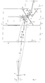
- a first silicon substrate 1 with plane-parallel broad sides 11, 14 carries, on a first broad side 11 as a transmission component 12, a transmission laser which is fastened with the aid of a mounting layer 13.
- the beam emerging from the light exit surface 120 on the end face of the transmission laser 12 with the center beam 121 at the transmission wavelength ⁇ 1 strikes an inclined surface 21.
- This surface is preferably generated by an anisotropic etching process in a second silicon substrate 2.
- the structuring of the second silicon substrate 2 can advantageously be done by structuring a silicon wafer in multiple uses. Only one use is shown in FIG. 1.
- n 0 is the refractive index in the space between the first broad side 11 of the substrate 1, the filter layer 22 and the light exit surface 120.
- This space can be filled with air in a first embodiment of the invention (case 1) or with a transparent adhesive in a second embodiment (case 2).
- the first broad side 11 is covered with an antireflection layer at least in the area of the beam entrance.
- a lens 15 is provided on the second broad side 14 of the substrate 1 as a structured surface area for focusing the transmission beam.
- this lens is structured as an integrated lens directly on the silicon substrate 1 in multiple uses.
- the surface of the lens is covered with an anti-reflection layer.
- This lens has the task of converting the diverging beam bundle emerging from the laser into a converging beam bundle and thereby imaging the light exit surface 120 onto a coupling surface within the end face 42 of an optical fiber 4 (namely in the core 41).
- an angle ⁇ 4 must be included between the normal to the end face 42 and the direction of the center beam 124 of the converging beam, which is greater than the angle of convergence between the center beam and an edge beam of the converging beam.
- an incident beam must also be coupled in at an angle to the fiber axis in order to avoid coupling losses due to angular misalignment.
- the axis of the socket and thus also an inserted plug must be guided perpendicular to the mounting surface of the receptacle.
- the magnification ratio for the beam transformation can be set by selecting the radius of curvature.
- the beam emerging from the semiconductor laser which can be regarded approximately as a Gaussian beam, is transformed such that the waist of the transformed laser beam is as large as the beam waist of a light wave guided in the single-mode fiber.
- LD laser diode
- R K 1100 ⁇ m Radius of the Si lens
- g 649 ⁇ m optical path lens - fiber (image width)
- b 1404 ⁇ m
- the waist size and the beam direction can be chosen by choosing the lens curvature radius R K of 1100 ⁇ m or 825 ⁇ m and the lens offset ⁇ X Li of 120 ⁇ m or 147 ⁇ m adjust that an optimal coupling into a single-mode fiber aligned perpendicular to the mounting plane of the laser is possible.
- the calculation for the propagation of the beams is also valid for the reverse light path according to the reciprocity principle of optics.
- the dichroic filter layer 22 has a very low reflectivity and a very high transmittance for the received beam because of its different wavelength.
- the received beam is therefore not reflected here, but rather enters the interior of the silicon substrate 2.
- the receiving beam is broken to the plumb line on the surface 21.
- an anisotropically etched recess 3 is produced in the side 24 of the substrate 2 in accordance with a development of the invention.
- the received light beam with the center beam 131 strikes the side surface 31 of the recess 3. Since the two surfaces 21 and 31 are parallel to one another because of the same anisotropic etching process, the angle of incidence ⁇ is for the two cases with air or a transparent adhesive on the left side of the surface 21 3L or ⁇ 3K of the center beam 131 on the boundary surface 31 is as large as the refraction angle ⁇ 2L or ⁇ 2K on the right side of the surface 21.
- the angle of incidence is smaller than the critical angle of total reflection, so that the light can emerge from the silicon substrate .
- this surface is covered with an anti-reflection layer 32.
- the same filter layer as in layer 22 can also be used here. In this case, both sides of the silicon wafer 2 can be coated in the same vacuum process.
- the recess 3 can either with air or with be filled with a transparent adhesive. Depending on Refractive index in the recess 3 result for the Refractive angles of the two cases 1 and 2 following Combinations:
- a photodiode can be used the active area on the top, as in FIG. 1 shown, or a photodiode with the active area the bottom can be used.
- the lateral position the photodiode can use the above Direction angle and the position of the recess 3 predetermined with respect to area 21 and by marks or latching structures on the side 24 of the silicon substrate 2 are marked, so that a passive Adjustment of this receiving diode is possible.
- the transformed receiving beam waist at point P 5 then has the same diameter as the beam waist of the laser beam at the light exit surface at point P 0 of the laser. In the example given, this is 4.5 ⁇ m. This means that even small-area photodiodes that are required for the highest frequency ranges (diameter of the active zone typically 30 ⁇ m) can still be coupled with sufficient adjustment latitude.
- the assembly of the optoelectronic Transducer elements can also be inexpensive Wafer level.
- the mutual orientation of the Upper and lower silicon substrates can advantageously happen at the wafer level. Doing so with all sub-substrates of both in a single adjustment process Wafers aligned with each other at the same time. This Alignment can also be done without adjustment if on the Wafers at least two places to each other corresponding locking structures together with the anisotropic etching of the other structures become.
- These locking structures can, for example be pyramid-shaped recesses, into which precision balls be inserted.
- the mutual fixation of the Both wafers can be glued, soldered or another known fastening method happen. After Fixation, the wafers are separated and the individual Module blocks mounted on the lead frames.
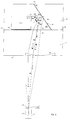
- FIG. 2 shows an inventive transceiver module that is mounted on one side 201 of a lead frame 200.
- Socket 300 On the other side 202 of leadframe 200 is one Socket 300 actively adjusted with its flange surface 301 and fixed via laser welding spots 203.
- the socket is a ferrule 400 with the transmission fiber 4 introduced.
- This fiber has an oblique cut Face (the cutting angle in this Embodiment is 8 °) in which the transformed Laser beam 124 is coupled.
- the axial distance will be preset by the stop ring 310 so that between the lens 15 on the underside 14 of the Silicon substrate 1 and the waist of the transformed Laser beam 124 just the image width calculated above b lies.
- the lateral position of the fiber with respect to the Beam waist of the transformed laser beam is through active adjustment of the flange surface 301 on the underside 202 of the leadframe 200 set and by laser welding spots 203 fixed.
- the one emerging from the back of the laser chip Light signal can, as is customary in the prior art, can be used for power control.
- the structure according to the invention offers an advantageous one for this Solution for beam deflection on a planar mounted Monitor diode 60.
- This monitor diode is invented mounted in a recess 16 in the silicon substrate 1.
- the top silicon substrate 2 receives another anisotropic etched surface 61 opposite surface 21.
- Both Surfaces 21 and 61 are the side surfaces of anisotropic etched opening 20 in the upper silicon substrate 2.
- the beam deflection of the rear emerging Laser beam is done by reflection on surface 61, for this purpose with a reflecting the laser wavelength Layer 62 is occupied.
- This can advantageously Layer 62 have the same structure as that dichroic layer 22 on the surface 21 and with it produced together without significant additional effort become.
- the bottom of the monitor diode 60 becomes the bottom and at least one of the side surfaces of the recess 16 with a gold layer 17 occupied.
- the rest of the electrical Contacting the receiving and transmitting branch of the Transceiver module is done via bond wires to the corresponding contact areas of the leadframe (not here drawn).
- the active components of the transceiver and the bond wires with an optically transparent protective potting compound top) 70 The entire module can then still be used surrounded by a hard covering (not shown here) become.
- an integrated transceiver chip 512 (FIG. 3) can also be used.
- a transceiver chip contains, integrated on a chip, a transmission part which emits the wavelength ⁇ 1 and a reception part which receives the reception wavelength ⁇ 2 .
- the transmitted and received light are routed via the same input and output waveguide on the chip and have the same light entry and exit spot that is located at point P 0 .
- this common input and output waveguide can be designed as a transformation waveguide to enlarge the mode field diameter.
- the beam paths for the send and receive directions are then as previously described for the send direction.
- the dichroic filter layer 22 is now replaced by a reflection layer 522 for both wavelengths.
- the wavelengths are separated on the integrated transceiver chip by an integrated wavelength-selective coupler.
- the transceiver chip can also contain an integrated monitor diode, so that the monitor diode 60 according to FIG. 2 in the recess 16 with the surface 61 provided for beam deflection can be omitted.
Abstract
Description
Die Erfindung geht von der Gattung aus, wie im
unabhängigen Anspruch 1 angegeben.The invention is based on the genus, as in
Ein solches Modul ist aus der deutschen Patentschrift DE 195 27 026 C2 bekannt.Such a module is from the German patent DE 195 27 026 C2 known.
Die Erfindung befaßt sich mit einem Modul, insbesondere mit einem optischen Transceiver, der zum Einbau in ein Receptacle für Leadframe-Montagetechnik geeignet ist. In der deutschen Patentanmeldung 197 55 806.2 wurde ein Receptacle für Leadframe-Montagetechnik vorgeschlagen.The invention is concerned with a module, in particular with an optical transceiver that can be installed in a Receptacle is suitable for leadframe assembly technology. In the German patent application 197 55 806.2 was a Receptacle proposed for leadframe assembly technology.
Für die Montage in einem Receptical wird üblicherweise als Sendebauelement eine kantenemittierende Halbleiterlaserdiode mit integrierter Strahltransformation bevorzugt. Solche Halbleiterlaserdioden haben in Lichtausbreitungsrichtung nach dem aktiven Laserkanal auf dem gleichen Chip einen passiven Transformationswellenleiter, der den Modenfelddurchmesser des Lasers von ca.1 µm auf ca. 4,5 µm vergrößert und somit eine bessere Anpassung an den Modenfelddurchmesser einer Einmodenfaser von 10 µm ermöglicht. Gleichzeitig wird bei dieser Strahltransformation der Abstrahlwinkel von ca. 30° auf etwa 12° reduziert. Solche nach dem Stand der Technik bekannten Laserdioden mit Strahltransformation (engl.: SSC-Laser = Spot Size Converted Laserdiode) werden üblicherweise für die Direktankopplung einer Einmodenfaser verwendet. Der Laser strahlt dabei in eine an seiner Stirnseite in geringem Abstand angeordnete Faser ein (Stirnflächenkopplung). Die Faserachse muß dazu in der Montageebene (Emissionsrichtung) des Lasers verlaufen. Dabei kann der Laser durch Rückreflexionen an der Faserstirnfläche in seiner Abstrahlcharakteristik gestört werden.For assembly in a Receptical is usually considered Transmitting device an edge emitting Semiconductor laser diode with integrated beam transformation prefers. Such semiconductor laser diodes have in Direction of light propagation after the active laser channel the same chip a passive Transformation waveguide, the mode field diameter of the laser enlarged from approx. 1 µm to approx. 4.5 µm and thus a better adaptation to the mode field diameter of a Single mode fiber of 10 µm enables. At the same time this beam transformation the beam angle of approx. 30 ° reduced to about 12 °. Such according to the prior art known laser diodes with beam transformation SSC laser = spot size converted laser diode) usually for the direct coupling of a single-mode fiber used. The laser shines in one on his End face arranged at a short distance (End face coupling). The fiber axis must be in the Mounting level (emission direction) of the laser. The laser can cause back reflections on the face of the fiber disturbed in its radiation characteristics become.
Bei der Verwendung des Lasers in einem Receptacle mit Leadframe-Montagetechnik verläuft die Achse der Steckbuchse und damit der optischen Faser senkrecht zur Emissionsrichtung (Montageebene) des Lasers, daher ist hier die oben beschriebene Stirnflächenkopplung nicht möglich. Bei einem Transceiver, der zusätzlich zu einem Sendeelement (z. B. Sendelaser) noch ein Empfangselement (z. B. Fotodiode) aufweist, läßt sich außerdem bei einer Direktankopplung der Faser an den Laser wegen des erforderlichen geringen Abstandes zwischen den Stirnflächen von Laser und Faser kein strahlteilendes Element zur Trennung der Sende- von der Empfangsstrahlung unterbringen. When using the laser in a receptacle with Leadframe assembly technology runs the axis of the Socket and thus the optical fiber perpendicular to Emission direction (mounting level) of the laser, therefore here the end face coupling described above is not possible. For a transceiver that is in addition to a Transmitting element (e.g. transmitting laser) still a receiving element (e.g. photodiode) can also be used in a Direct coupling of the fiber to the laser because of the required small distance between the End faces of laser and fiber no beam splitting Element for separating the transmission radiation from the reception radiation accommodate.
Der Anmeldungsgegenstand mit den Merkmalen des Anspruches
1 hat folgenden Vorteil:
Das Modul ist für den Einbau in ein Receptacle geeignet
und im Großnutzen kostengünstig herstellbar. Es kann als
Sendemodul oder Transceiver ausgebildet sein.The subject of the application with the features of
The module is suitable for installation in a receptacle and can be manufactured inexpensively for large-scale use. It can be designed as a transmitter module or transceiver.
Vorteilhafte Weiterbildungen sind in den abhängigen Ansprüchen angegeben, deren Merkmale auch, soweit sinnvoll, miteinander kombiniert werden können.Advantageous further developments are in the dependent Claims specified, the characteristics of which, to the extent useful, can be combined with each other.
Während bei dem Modul für Leadframe-Montagetechnik nach der deutschen Patentanmeldung 197 55 806.2 für die Sende- und für die Empfangsrichtung zwei getrennte optische Wellenleiter und somit zwei Steckbuchsen und je ein getrenntes Sende- und Empfangsteil vorgesehen sind, ist ein Transceiver-Modul nach einer Weiterbildung der vorliegenden Erfindung für nur einen optischen Wellenleiter für die Sende- und Empfangsrichtung vorgesehen. Dabei werden für die Sende- und die Empfangssignale zwei unterschiedliche Wellenlängen verwendet. Zur Richtungstrennung zwischen Sende- und Empfangspfad dient ein wellenlängenselektives Filter.While with the module for leadframe assembly technology after German patent application 197 55 806.2 for the broadcast and for the receiving direction two separate optical Waveguide and thus two sockets and one each separate transmitting and receiving part are provided a transceiver module after further training present invention for only one optical Waveguide for the send and receive direction intended. It is for the broadcast and Receive signals two different wavelengths used. To separate the direction between the send and receive path serves a wavelength selective filter.
Ausführungsbeispiele der Erfindung sind in der Zeichnung dargestellt und im Folgenden näher erläutert. Dabei sind bei mehreren Figuren jeweils dieselben Bezugszeichen für im wesentlichen gleiche Teile verwendet. Schematisch ist jeweils im Schnitt gezeigt in
- Figur 1:
- ein Transceiver-Modul nach der Erfindung, mit Strahlengang,
- Figur 2:
- ein Transceiver-Modul, das auf einer Seite eines Leadframe montiert ist,
- Figur 3:
- ein Transceiver-Modul mit integriertem Transceiver-Chip als Sendeelement.
- Figure 1:
- a transceiver module according to the invention, with beam path,
- Figure 2:
- a transceiver module that is mounted on one side of a lead frame,
- Figure 3:
- a transceiver module with an integrated transceiver chip as a transmission element.
Fig. 1 zeigt den Aufbau und den Strahlengang für ein
Ausführungsbeispiel eines erfindungsgemäßen Transceiver-Moduls.
Ein erstes Siliziumsubstrat 1 mit planparallelen
Breitseiten 11, 14 trägt auf einer ersten Breitseite 11
als Sendebauelement 12 einen Sendelaser, der mit Hilfe
einer Montageschicht 13 befestigt ist. Das aus der
Lichtaustrittsfläche 120 auf der Stirnfläche des
Sendelasers 12 austretende Strahlenbündel mit dem
Mittenstrahl 121 bei der Sendewellenlänge λ1 trifft auf
eine geneigte Fläche 21. Bevorzugt wird diese Fläche durch
einen anisotropen Ätzprozeß in einem zweiten Siliziumsubstrat
2 erzeugt. Die Strukturierung des zweiten
Siliziumsubstrats 2 kann hierbei vorteilhafterweise durch
Strukturierung eines Siliziumwafers im Vielfachnutzen geschehen.
In der Fig. 1 ist nur ein Nutzen dargestellt. Die
Fläche 21 ist mit einer dichroitischen Filterschicht 22
beschichtet, welche die Sendewellenlänge λ1 reflektiert
und die Empfangswellenlänge λ2 durchläßt. Durch den
anisotropen Silizium-Ätzprozeß bedingt, weist die Fläche
21 eine kristallographische (111)-Orientierung auf und ist
gegenüber der (100)-orientierten Montagefläche 23 des
Siliziumsubstrates 2 unter einem Böschungswinkel von
Für die beiden Fälle mit Luft bzw. Kleber oberhalb der
ersten Breitseite 11 des Substrates 1 läßt sich durch Wahl
des Linsenkrümmungsradius RK von 1100 µm bzw. 825 µm und
des Linsenversatzes ΔXLi von 120 µm bzw. 147 µm die
Taillengröße und die Strahlrichtung so anpassen, daß eine
optimale Einkopplung in eine senkrecht zur Montageebene
des Lasers ausgerichtete Einmodenfaser möglich ist.For the two cases with air or adhesive above the first
Die Berechnung für die Ausbreitung der Strahlenbündel ist
nach dem Reziprozitätsprinzip der Optik ebenso auch für
den umgekehrten Lichtweg gültig. Das heißt, daß ein aus
der Faser austretender Empfangsstrahl bis zum Auftreffen
auf die dichroitische Filterschicht 22 die gleiche
Transformation und Strahlumlenkung erfährt wie der
Sendestrahl. Die dichroitische Filterschicht 22 hat für
den Empfangsstrahl wegen dessen anderer Wellenlänge ein
sehr geringes Reflexionsvermögen und ein sehr hohes
Transmissionsvermögen. Der Empfangsstrahl wird hier also
nicht reflektiert, sondern er tritt in das Innere des
Siliziumsubstrats 2 ein. Der Einfallswinkel α2 des
Mittenstrahls ist hier ebenso wie beim einfallenden
Sendestrahl der Winkel β = 35,3°. An der Fläche 21 wird
der Empfangsstrahl zum Lot hingebrochen. Der
Brechungswinkel hinter der Fläche 21 ist
Für den Fall 1 mit n0 = n0L = 1 für Luft und n2 = nSi =
3,4777 für Silizium als Substratmaterial für das Substrat
2 erhält man
Um das Empfangslicht trotzdem aus dem Siliziumsubstrat 2
auskoppeln und in eine planar auf der Seite 24 montierte
Empfangsdiode 5 einkoppeln zu können, ist entsprechend
einer Weiterbildung der Erfindung eine anisotrop geätzte
Vertiefung 3 in der Seite 24 des Substrates 2 erzeugt. Das
Empfangslichtbündel mit dem Mittenstrahl 131 trifft auf
die Seitenfläche 31 der Vertiefung 3. Da die beiden
Flächen 21 und 31 wegen des gleichen anisotropen
Ätzprozesses parallel zueinander sind, ist für die beiden
Fälle mit Luft bzw. einem transparenten Kleber linksseitig
der Fläche 21 der Einfallswinkel β3L bzw. β3K des Mittenstrahls
131 an der Begrenzungsfläche 31 so groß wie der
Brechungswinkel β2L bzw. β2K rechtsseitig der Fläche 21. In
beiden Fällen ist der Einfallswinkel kleiner als der
Grenzwinkel der Totalreflexion, so daß das Licht aus dem
Siliziumsubstrat austreten kann. Um Verluste durch
Fresnelreflexionen an der Grenzfläche 31 zu vermeiden, ist
diese Fläche mit einer Antireflexionsschicht 32 belegt.
Anstelle einer Antireflexionsschicht kann hier auch die
gleiche Filterschicht wie in Schicht 22 verwendet werden.
In diesem Fall können beide Seiten des Siliziumwafers 2 im
gleichen Vakuumprozeß beschichtet werden.In order to be able to decouple the receiving light from the
Die Vertiefung 3 kann entweder mit Luft oder auch mit
einem transparentem Kleber gefüllt sein. Je nach
Brechungsindex in der Vertiefung 3 ergeben sich für die
Brechungswinkel der beiden Fälle 1 und 2 folgende
Kombinationen:The recess 3 can either with air or with
be filled with a transparent adhesive. Depending on
Refractive index in the recess 3 result for the
Refractive angles of the two
Auf der Seite 24 des zweiten Siliziumsubstrates 2 wird die
als Empfangselement dienende Empfangsdiode 5 so montiert,
daß ihre lichtempfindliche Fläche über der Öffnung 33 der
Vertiefung 3 liegt. Dabei kann entweder eine Fotodiode mit
der aktiven Fläche auf der Oberseite, wie in Fig. 1
gezeigt, oder eine Fotodiode mit der aktiven Fläche auf
der Unterseite eingesetzt werden. Die laterale Position
der Fotodiode kann anhand der oben angegebenen
Richtungswinkel und der Position der Vertiefung 3
bezüglich der Fläche 21 vorherbestimmt und durch Marken
oder Raststrukturen auf der Seite 24 des Siliziumsubstrates
2 gekennzeichnet werden, so daß eine passive
Justierung dieser Empfangsdiode möglich ist. On the
Die optischen Weglängen (= geometrische Weglänge geteilt
durch den Brechungsindex des jeweils durchlaufenen
Materials) zwischen dem Lichtaustrittspunkt P0 an der
Laserstirnfläche und dem Auftreffpunkt P21 des
Sendestrahls 121 auf der Fläche 21 einerseits und des
Empfangslichtstrahls zwischen dem Punkt P21 und dem
Lichtauftreffpunkt P5 auf der Empfangsdiode 5 andererseits
lassen sich durch eine geeignete Positionierung der
Vertiefung 3 bezüglich der Fläche 21 einander angleichen.Dadurch
kann erreicht werden, daß im Punkt P5 die
Strahltaille des transformierten Empfangsstrahls zu liegen
kommt, die als Abbildung der Strahltaille auf der
Faserstirnfläche 42 durch die Linse 15 entsteht. Die
transformierte Emfangsstrahltaille im Punkt P5 hat dann
den gleichen Durchmesser wie die Strahltaille des
Laserstrahls an der Lichtaustrittsfläche im Punkt P0 des
Lasers. In dem angegebenen Beispiel sind dies 4,5 µm.
Damit lassen sich auch kleinflächige Fotodioden, die für
höchste Frequenzbereiche erforderlich sind (Durchmesser
der aktiven Zone typisch 30 µm) noch mit ausreichendem
Justagespielraum ankoppeln.The optical path lengths (= geometric path length divided by the refractive index of the material being traversed) between the light exit point P 0 on the end face of the laser and the point of incidence P 21 of the
Für das erfindungsgemäße Modul ist eine kostengünstige
Herstellung der Siliziumsubstrate 1 und 2 möglich, da sie
im Großnutzen auf Waferebene strukturiert und beschichtet
werden können. Die Montage der optoelektronischen
Wandlerelemente kann ebenfalls kostengünstig auf
Waferebene erfolgen. Auch die gegenseitige Ausrichtung des
oberen und unteren Siliziumsubstrates kann vorteilhafterweise
auf Waferebene geschehen. Dabei werden mit
einem einzigen Justagevorgang alle Teilsubstrate beider
Wafer gleichzeitig zueinander ausgerichtet. Diese
Ausrichtung kann auch justagefrei erfolgen, wenn auf dem
Wafer an mindestens zwei Stellen zueinander
korrespondierende Raststrukturen gemeinsam mit der
anisotropen Ätzung der übrigen Strukturen hergestellt
werden. Diese Raststrukturen können beispielsweise
pyramidenförmige Vertiefungen sein, in welche Präzisionskugeln
eingelegt werden. Die gegenseitige Fixierung der
beiden Wafer kann durch Kleben, Löten oder ein anderes
bekanntes Befestigungsverfahren geschehen. Nach der
Fixierung werden die Wafer vereinzelt und die einzelnen
Modulbausteine auf den Leadframes montiert.For the module according to the invention is an inexpensive one
Production of
Fig. 2 zeigt ein erfindungsgemäßes Transceiver-Modul, das
auf einer Seite 201 eines Leadframe 200 montiert ist. Auf
der anderen Seite 202 des Leadframe 200 ist eine
Steckbuchse 300 mit ihrer Flanschfläche 301 aktiv justiert
und über Laserschweißpunkte 203 fixiert. In diese
Steckbuchse ist eine Ferrule 400 mit der Übertragungsfaser
4 eingeführt. Diese Faser hat eine schräg geschnittene
Stirnfläche (der Schnittwinkel in diesem
Ausführungsbeispiel ist 8°), in die der transformierte
Laserstrahl 124 eingekoppelt wird. Der axiale Abstand wird
dabei durch den Anschlagring 310 so voreingestellt, daß
zwischen der Linse 15 auf der Unterseite 14 des
Siliziumsubstrates 1 und der Taille des transformierten
Laserstrahls 124 gerade die oben berechnete Bildweite b
liegt. Die laterale Position der Faser bezüglich der
Strahltaille des transformierten Laserstrahls wird durch
aktive Justage der Flanschfläche 301 auf der Unterseite
202 des Leadframes 200 eingestellt und durch Laserschweißpunkte
203 fixiert. 2 shows an inventive transceiver module that
is mounted on one
Das aus der Rückseite des Laserchips austretende
Lichtsignal kann, wie nach dem Stand der Technik üblich,
zur Leistungsregelung verwendet werden. Der
erfindungsgemäße Aufbau bietet hierzu eine vorteilhafte
Lösung zur Strahlumlenkung auf eine planar montierte
Monitordiode 60. Diese Monitordiode wird erfindungsgemäß
in einer Vertiefung 16 im Siliziumsubstrat 1 montiert. Das
obere Siliziumsubstrat 2 erhält eine weitere anisotrop
geätzte Fläche 61, die der Fläche 21 gegenüberliegt. Beide
Flächen 21 und 61 sind dabei die Seitenflächen einer anisotrop
geätzten Öffnung 20 im oberen Siliziumsubstrat 2.
Die Strahlumlenkung des rückwärtig austretenden
Laserstrahls geschieht durch Reflexion an der Fläche 61,
die hierzu mit einer die Laserwellenlänge reflektierenden
Schicht 62 belegt ist. Vorteilhafterweise kann diese
Schicht 62 den gleichen Aufbau haben, wie die
dichroitische Schicht 22 auf der Fläche 21 und mit dieser
gemeinsam ohne wesentlichen Mehraufwand hergestellt
werden. Zur elektrischen und mechanischen Kontaktierung
der Unterseite der Monitordiode 60 wird der Boden und
mindestens eine der Seitenflächen der Vertiefung 16 mit
einer Goldschicht 17 belegt. Die übrige elektrische
Kontaktierung des Empfangs- und Sendezweigs des
Transceiver-Moduls geschieht über Bonddrähte zu den
entsprechenden Kontaktbereichen des Leadframes (hier nicht
gezeichnet). Zum Schutz vor Umwelteinflüssen können die
aktiven Bauelemente des Transceivers und die Bonddrähte
mit einem optisch transparenten Schutzverguß (engl. glob
top) 70 umhüllt sein. Das Gesamtmodul kann dann noch mit
einer harten Umhüllung (hier nicht gezeichnet) umgeben
werden. The one emerging from the back of the laser chip
Light signal can, as is customary in the prior art,
can be used for power control. Of the
The structure according to the invention offers an advantageous one for this
Solution for beam deflection on a planar mounted
Anstelle des Laserchips 12 kann auch ein integrierter
Transceiverchip 512 (Fig. 3) eingesetzt werden. Ein
solcher Transceiverchip enthält auf einem Chip integriert
einen Sendeteil, der die Wellenlänge λ1 aussendet und
einen Empfangsteil, der die Empfangswellenlänge λ2
empfängt. Das Sende- und das Empfangslicht werden über
denselben Ein- und Ausgangswellenleiter auf dem Chip
geführt und haben denselben Lichtein- und -austrittsfleck,
der an der Stelle P0 liegt. Dieser gemeinsame Ein- und
Ausgangswellenleiter kann, wie zuvor beschrieben, als
Transformationswellenleiter zur Vergrößerung des
Modenfelddurchmessers ausgebildet sein. Die Strahlengänge
für die Sende- und die Empfangsrichtung sind dann so, wie
zuvor für die Senderichtung beschrieben wurde. Die
dichroitische Filterschicht 22 wird nun durch eine
Reflexionsschicht 522 für beide Wellenlängen ersetzt. Die
Trennung der Wellenlängen geschieht auf dem integrierten
Transceiverchip durch einen dort integrierten
wellenlängenselektiven Koppler. Zusätzlich kann der
Transceiverchip auch eine integrierte Monitordiode
enthalten, so daß die Monitordiode 60 nach Figur 2 in der
Vertiefung 16 mit der zur Strahlumlenkung vorgesehenen
Fläche 61 entfallen kann.Instead of the
Ebenso ist es möglich, die erfindungsgemäße Anordnung ganz
ohne Empfangsteil, also ohne die Fotodiode 5 und ohne die
Vertiefung 3 nur mit dem Laserchip 12 als reines
Sendemodul zu verwenden.It is also possible to completely dispose of the arrangement according to the invention
without receiving part, ie without the
Claims (13)
Applications Claiming Priority (2)
| Application Number | Priority Date | Filing Date | Title |
|---|---|---|---|
| DE19810624 | 1998-03-12 | ||
| DE19810624A DE19810624A1 (en) | 1998-03-12 | 1998-03-12 | Electro-optical module |
Publications (2)
| Publication Number | Publication Date |
|---|---|
| EP0942302A2 true EP0942302A2 (en) | 1999-09-15 |
| EP0942302A3 EP0942302A3 (en) | 2002-07-17 |
Family
ID=7860555
Family Applications (1)
| Application Number | Title | Priority Date | Filing Date |
|---|---|---|---|
| EP98117620A Withdrawn EP0942302A3 (en) | 1998-03-12 | 1998-09-17 | Electrooptical module |
Country Status (2)
| Country | Link |
|---|---|
| EP (1) | EP0942302A3 (en) |
| DE (1) | DE19810624A1 (en) |
Cited By (2)
| Publication number | Priority date | Publication date | Assignee | Title |
|---|---|---|---|---|
| WO2001086337A1 (en) * | 2000-05-08 | 2001-11-15 | Infineon Technologies Ag | Optoelectronic coupling element and method for producing the same |
| WO2004086519A1 (en) * | 2003-03-24 | 2004-10-07 | Hymite A/S | Package with a light emitting device |
Families Citing this family (7)
| Publication number | Priority date | Publication date | Assignee | Title |
|---|---|---|---|---|
| DE10002329A1 (en) | 2000-01-20 | 2001-08-02 | Infineon Technologies Ag | Manufacturing process for an optical transmitter assembly |
| DE10003087A1 (en) * | 2000-01-25 | 2001-09-13 | Infineon Technologies Ag | Arrangement for an optoelectronic transmitter and receiver module |
| DE10004411A1 (en) | 2000-02-02 | 2001-08-16 | Infineon Technologies Ag | Electro-optical transmitter / receiver module and method for its production |
| DE10312500B4 (en) | 2003-03-14 | 2007-11-08 | Infineon Technologies Ag | Arrangement for multiplexing and / or demultiplexing optical signals of a plurality of wavelengths |
| US20050063431A1 (en) * | 2003-09-19 | 2005-03-24 | Gallup Kendra J. | Integrated optics and electronics |
| US7520679B2 (en) * | 2003-09-19 | 2009-04-21 | Avago Technologies Fiber Ip (Singapore) Pte. Ltd. | Optical device package with turning mirror and alignment post |
| US9470857B2 (en) * | 2014-06-13 | 2016-10-18 | Sumitomo Electric Industries, Ltd. | Optical module with beam splitter on reflecting surface |
Citations (5)
| Publication number | Priority date | Publication date | Assignee | Title |
|---|---|---|---|---|
| US4730330A (en) * | 1985-01-07 | 1988-03-08 | Siemens Aktiengesellschaft | Integrated structure for bi-directional optical fiber transmission |
| US4807238A (en) * | 1986-03-12 | 1989-02-21 | Ricoh Co., Ltd. | A semiconductor laser device |
| US5479540A (en) * | 1994-06-30 | 1995-12-26 | The Whitaker Corporation | Passively aligned bi-directional optoelectronic transceiver module assembly |
| US5566265A (en) * | 1993-12-22 | 1996-10-15 | Siemens Aktiengesellschaft | Transmission and reception module for a bidirectional, optical message and signal transmission |
| DE19616969A1 (en) * | 1996-04-27 | 1997-10-30 | Bosch Gmbh Robert | Optical assembly for coupling an optical waveguide and method for producing the same |
-
1998
- 1998-03-12 DE DE19810624A patent/DE19810624A1/en not_active Withdrawn
- 1998-09-17 EP EP98117620A patent/EP0942302A3/en not_active Withdrawn
Patent Citations (5)
| Publication number | Priority date | Publication date | Assignee | Title |
|---|---|---|---|---|
| US4730330A (en) * | 1985-01-07 | 1988-03-08 | Siemens Aktiengesellschaft | Integrated structure for bi-directional optical fiber transmission |
| US4807238A (en) * | 1986-03-12 | 1989-02-21 | Ricoh Co., Ltd. | A semiconductor laser device |
| US5566265A (en) * | 1993-12-22 | 1996-10-15 | Siemens Aktiengesellschaft | Transmission and reception module for a bidirectional, optical message and signal transmission |
| US5479540A (en) * | 1994-06-30 | 1995-12-26 | The Whitaker Corporation | Passively aligned bi-directional optoelectronic transceiver module assembly |
| DE19616969A1 (en) * | 1996-04-27 | 1997-10-30 | Bosch Gmbh Robert | Optical assembly for coupling an optical waveguide and method for producing the same |
Cited By (4)
| Publication number | Priority date | Publication date | Assignee | Title |
|---|---|---|---|---|
| WO2001086337A1 (en) * | 2000-05-08 | 2001-11-15 | Infineon Technologies Ag | Optoelectronic coupling element and method for producing the same |
| US6488418B2 (en) | 2000-05-08 | 2002-12-03 | Infineon Technologies Ag | Optoelectronic coupling element and production method |
| WO2004086519A1 (en) * | 2003-03-24 | 2004-10-07 | Hymite A/S | Package with a light emitting device |
| US6856717B2 (en) | 2003-03-24 | 2005-02-15 | Hymite A/S | Package with a light emitting device |
Also Published As
| Publication number | Publication date |
|---|---|
| DE19810624A1 (en) | 1999-09-16 |
| EP0942302A3 (en) | 2002-07-17 |
Similar Documents
| Publication | Publication Date | Title |
|---|---|---|
| DE102005019562B4 (en) | Optical transmitting and receiving module | |
| EP0360177B1 (en) | Optical transmitting and/or receiving element | |
| EP0706069B1 (en) | Transmitting and receiving module for bidirectional optical communication and signal transmission | |
| EP0664585B1 (en) | Transmitter and receiver module for bi-directional optical communication | |
| EP1425619B1 (en) | Transmitter and receiver arrangement for bi-directional optic data transmission | |
| EP0395854B1 (en) | Arrangement for connecting a light wave conductor to an optical transmitter or receiver | |
| DE19640423C1 (en) | Optoelectronic module for bidirectional optical data transmission | |
| DE19617921C2 (en) | Integrated optical module with waveguide and photo receiving device | |
| EP0631163B1 (en) | Bidirectional optical transceiver | |
| DE4440976A1 (en) | Optical transmitter and receiver with a surface emitting laser | |
| EP0600267A1 (en) | Optical bidirectional transmit/receive module | |
| EP2320215B1 (en) | Semiconductor laser system for gas detection with integrated and thermally controlled beam shaping element | |
| DE102016221806B4 (en) | Wavelength-division multiplexing unit, wavelength-division multiplexing system and method of forming a wavelength-division multiplexing unit | |
| DE19616969A1 (en) | Optical assembly for coupling an optical waveguide and method for producing the same | |
| DE4446328A1 (en) | Transceiver module for optical communication | |
| DE19510559C1 (en) | Optical communication transceiver with two incoming beam reflectors | |
| EP0942302A2 (en) | Electrooptical module | |
| DE10201127C2 (en) | Arrangement for coupling and / or decoupling optical signals from at least one optical data channel into or out of an optical waveguide | |
| DE112008003958T5 (en) | Nanowire optical block devices for amplifying, modulating and detecting optical signals | |
| DE19607107A1 (en) | Light conductor to opto-electronic component coupling apparatus for optical communications | |
| DE19640421A1 (en) | Optoelectronic module for bidirectional optical data transmission | |
| DE102004038530B3 (en) | Method and device for producing an optical connection between an optoelectronic component and an optical waveguide | |
| WO1998050811A1 (en) | Electrooptical module | |
| EP1568158B1 (en) | Bidirectional emitting and receiving module | |
| DE19718949A1 (en) | Electro-optical module |
Legal Events
| Date | Code | Title | Description |
|---|---|---|---|
| PUAI | Public reference made under article 153(3) epc to a published international application that has entered the european phase |
Free format text: ORIGINAL CODE: 0009012 |
|
| AK | Designated contracting states |
Kind code of ref document: A2 Designated state(s): AT BE CH CY DE DK ES FI FR GB GR IE IT LI LU MC NL PT SE |
|
| AX | Request for extension of the european patent |
Free format text: AL;LT;LV;MK;RO;SI |
|
| PUAL | Search report despatched |
Free format text: ORIGINAL CODE: 0009013 |
|
| AK | Designated contracting states |
Kind code of ref document: A3 Designated state(s): AT BE CH CY DE DK ES FI FR GB GR IE IT LI LU MC NL PT SE |
|
| AX | Request for extension of the european patent |
Free format text: AL;LT;LV;MK;RO;SI |
|
| STAA | Information on the status of an ep patent application or granted ep patent |
Free format text: STATUS: THE APPLICATION IS DEEMED TO BE WITHDRAWN |
|
| 18D | Application deemed to be withdrawn |
Effective date: 20020403 |