EP0943177B1 - Clock vernier adjustment - Google Patents
Clock vernier adjustment Download PDFInfo
- Publication number
- EP0943177B1 EP0943177B1 EP97951512A EP97951512A EP0943177B1 EP 0943177 B1 EP0943177 B1 EP 0943177B1 EP 97951512 A EP97951512 A EP 97951512A EP 97951512 A EP97951512 A EP 97951512A EP 0943177 B1 EP0943177 B1 EP 0943177B1
- Authority
- EP
- European Patent Office
- Prior art keywords
- edge
- clock signal
- falling
- rising
- memory
- Prior art date
- Legal status (The legal status is an assumption and is not a legal conclusion. Google has not performed a legal analysis and makes no representation as to the accuracy of the status listed.)
- Expired - Lifetime
Links
- 230000015654 memory Effects 0.000 claims abstract description 205
- 230000003111 delayed effect Effects 0.000 claims abstract description 31
- 230000001960 triggered effect Effects 0.000 claims abstract description 6
- 230000001934 delay Effects 0.000 claims description 19
- 238000000034 method Methods 0.000 claims description 10
- 239000000872 buffer Substances 0.000 description 39
- 101000885321 Homo sapiens Serine/threonine-protein kinase DCLK1 Proteins 0.000 description 23
- 102100039758 Serine/threonine-protein kinase DCLK1 Human genes 0.000 description 23
- 238000010586 diagram Methods 0.000 description 16
- 230000000630 rising effect Effects 0.000 description 13
- 230000002457 bidirectional effect Effects 0.000 description 6
- 230000005540 biological transmission Effects 0.000 description 6
- 230000000694 effects Effects 0.000 description 6
- 230000007704 transition Effects 0.000 description 5
- 230000003139 buffering effect Effects 0.000 description 4
- 238000004891 communication Methods 0.000 description 4
- 230000000295 complement effect Effects 0.000 description 2
- 241001396014 Priacanthus arenatus Species 0.000 description 1
- 230000009286 beneficial effect Effects 0.000 description 1
- 230000001419 dependent effect Effects 0.000 description 1
- 238000005516 engineering process Methods 0.000 description 1
- 230000000977 initiatory effect Effects 0.000 description 1
- 238000005070 sampling Methods 0.000 description 1
- 230000003068 static effect Effects 0.000 description 1
- 238000009966 trimming Methods 0.000 description 1
Images


Classifications
-
- H—ELECTRICITY
- H03—ELECTRONIC CIRCUITRY
- H03K—PULSE TECHNIQUE
- H03K5/00—Manipulating of pulses not covered by one of the other main groups of this subclass
-
- G—PHYSICS
- G11—INFORMATION STORAGE
- G11C—STATIC STORES
- G11C7/00—Arrangements for writing information into, or reading information out from, a digital store
- G11C7/22—Read-write [R-W] timing or clocking circuits; Read-write [R-W] control signal generators or management
- G11C7/225—Clock input buffers
-
- G—PHYSICS
- G11—INFORMATION STORAGE
- G11C—STATIC STORES
- G11C7/00—Arrangements for writing information into, or reading information out from, a digital store
- G11C7/10—Input/output [I/O] data interface arrangements, e.g. I/O data control circuits, I/O data buffers
- G11C7/1051—Data output circuits, e.g. read-out amplifiers, data output buffers, data output registers, data output level conversion circuits
-
- G—PHYSICS
- G11—INFORMATION STORAGE
- G11C—STATIC STORES
- G11C7/00—Arrangements for writing information into, or reading information out from, a digital store
- G11C7/10—Input/output [I/O] data interface arrangements, e.g. I/O data control circuits, I/O data buffers
- G11C7/1078—Data input circuits, e.g. write amplifiers, data input buffers, data input registers, data input level conversion circuits
-
- G—PHYSICS
- G11—INFORMATION STORAGE
- G11C—STATIC STORES
- G11C7/00—Arrangements for writing information into, or reading information out from, a digital store
- G11C7/22—Read-write [R-W] timing or clocking circuits; Read-write [R-W] control signal generators or management
-
- G—PHYSICS
- G11—INFORMATION STORAGE
- G11C—STATIC STORES
- G11C8/00—Arrangements for selecting an address in a digital store
- G11C8/06—Address interface arrangements, e.g. address buffers
Definitions
- the present invention relates generally to integrated circuits, and more particularly to clock adjustments in memory systems, such as memory systems including dynamic random access memories (DRAMs).
- DRAMs dynamic random access memories
- Integrated circuits typically include a number of input/output pins which are used for communication with additional circuitry.
- an integrated memory device such as a dynamic random access memory (DRAM)
- DRAM dynamic random access memory
- control inputs for receiving memory operation control signals
- data pins for bi-directional data communication with an external system or processor.
- the data transmission rate of modern integrated circuits is primarily limited by internal circuitry operating speeds. That is, communication networks have been developed which can transmit signals between circuitry at a rate that is faster than the capacity of many integrated circuits.
- a group of integrated circuits can be combined on a common bus and be controlled by a common controller. In this configuration, each integrated circuit operates in a coordinated manner with the other integrated circuits to share data which is transmitted at a high speed.
- a group of memory devices such as DRAMs, static RAMs, or read only memories (ROM), can be connected to a common data bus and be controlled by a memory controller to form a memory system.
- the data rate of the bus may be substantially faster than the feasible operating speed of the individual memories.
- Each memory therefore, is operated so that while one memory is processing received data, another memory is receiving new data.
- Such a memory system with an appropriate number of memory devices and an efficient memory controller can achieve very high speed data transmissions.
- ANONYMUS "Pulse Combining Network"
- IBM Technical Disclosure Bulletin, Vol. 32, No. 12, May 1990, pages 149-151 discloses a circuit for providing complementary signals having their respective edges in alignment with each other.
- Two delay circuits are connected with their inputs to a clock signal line such that at the outputs of the two delay circuits said complementary signals are obtained.
- the present invention provides a method and integrated circuit including the features of the independent claims.
- the rising-edge and falling-edge delays are programmable delays.
- a rising edge delay circuit receives the input clock signal and provides the rising-edge clock signal
- a falling-edge delay circuit receives the rising-edge clock signal and providing the falling-edge clock signal.
- a falling-edge delay circuit receives the input clock signal and provides the falling-edge clock signal
- a rising-edge delay circuit receives the falling-edge clock signal and provides the rising-edge clock signal.
- One form of the present invention is a memory system including a memory controller and memory modules for storing data.
- a data bus carries write data from the memory controller to the memory modules and carries read data from the memory modules to the memory controller.
- a command bus carries commands from the memory controller to the memory modules.
- a clock line carries an input clock signal from the memory controller to the memory modules.
- Each memory module includes at least one vernier clock adjustment circuit receiving the input clock signal and providing a rising-edge clock signal representing the input clock signal delayed by a rising-edge delay and providing a falling-edge clock signal representing the input clock signal delayed by a falling-edge delay.
- Each memory module also includes at least one edge triggered circuit receiving read or write data and the rising-edge and falling-edge clock signals, and storing read or write data at the rising-edge of the rising-edge clock signal and at the falling-edge of the falling-edge clock signal.
- edge triggered circuit receiving read or write data and the rising-edge and falling-edge clock signals, and storing read or write data at the rising-edge of the rising-edge clock signal and at the falling-edge of the falling-edge clock signal.
- vernier adjustment circuitry can also be employed for clocking commands into the memory modules.
- the memory modules can include one or more memory integrated circuits, such as dynamic random access memories (DRAMs).
- DRAMs dynamic random access memories
- the vernier clock adjustment circuitry and method according to the present invention more accurately and precisely compensates for the effects of duty cycle variation, bus position of a given memory device, timing drift, loading variations, clock jitter, clock skew, noise, overshoot, and ringing by individually adjusting both the rising-edge and falling-edge timings interdependently from each other. As a result, data is accurately clocked in the memory devices even at higher data transmission rates.
- Figure 1 is a block diagram of one embodiment of a memory system.
- Figure 2 is a timing diagram illustrating the bus timing of the memory system of Figure 1.
- Figure 3 is a block diagram of another embodiment of a memory system.
- Figure 4 is a timing diagram illustrating the bus timing of the memory system of Figure 3.
- Figure 5 is a block diagram of another embodiment of a memory system.
- Figure 6 is a timing diagram illustrating the bus timing of the memory system of Figure 5.
- Figure 7 is a block diagram of a memory system having vernier clock adjustment circuitry.
- Figure 8A is a timing diagram illustrating an ideal signal waveform.
- Figure 8B is a timing diagram illustrating a non-ideal signal waveform.
- Figure 9 is a block diagram of an independent rising and falling edge vernier clock adjustment system.
- Figure 10 is a block diagram of an interdependent cascaded rising and falling edge vernier clock adjustment system.
- DRAM dynamic random access memory
- the present invention can, however, be implemented in any integrated circuit and other memory systems including other types of memory integrated circuits.
- the DRAM according to the present invention is similar in many respects to conventional DRAMs, such as those commercially available from Micron Technology, Inc. of Boise, Idaho. For clarity, only a portion of the well-known circuitry of the DRAM is described herein, while the new circuitry of the DRAM of the present invention is described in detail herein.
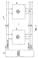
- a memory system is illustrated generally at 20 in Figure 1.
- Memory system 20 includes a memory controller 22 and N DRAM modules such as indicated at 24 and 26.
- the DRAM modules, such as modules 24 and 26, each comprise at least one DRAM device.
- a command bus 28 is an unidirectional bus for carrying address and control information from memory controller 22 to the DRAM modules. Address and control information is typically transferred from memory controller 22 on command bus 28 in uniform packets. For example, if a packet is four times the width of command bus 28, a command packet is transferred in four cycles on each edge of a free-running clock (CCLK) provided on a clock line 30 from memory controller 22.
- a data bus 32 is a bidirectional bus carrying write data from memory controller 22 to the DRAM modules and further carrying read data from the DRAM modules to memory controller 22. Two bidirectional data clocks, DCLK0 and DCLK1, are respectively provided on clock line 34 and clock line 36.
- Data clocks DCLK0 and DCLK1 are used to precisely transfer read data timing from the DRAM modules to the memory controller 22 and to further precisely transfer write data timing from memory controller 22 to the DRAM modules. Both rising edge and falling edge transitions of the selected DCLK are employed to clock the input latches of the DRAM modules and memory controller receiving data.
- the data clocks DCLK0 and DCLK1 follow the same path as data provided on data bus 32 to reduce the effects of clock jitter, duty cycle variation, bus position, drift timing, and loading variations.
- control of data bus 32 is transferred from one device in memory system 20 to another device in memory system 20, such as from memory controller 22 to DRAM module 24, from DRAM module 24 to memory controller 22, or from DRAM module 24 to DRAM module 26, one DCLK is deactivated and the other DCLK is activated.
- Memory controller 22 determines which DCLK is to be used for a given read or write operation and provides the information indicating which DCLK to use in the command packet provided on command bus 28.
- Memory system 20 accommodates for minimum and maximum delays from command at memory controller 22 to read data at memory controller 22 from the different DRAM modules by programming vernier clock adjustment circuits in each DRAM module.
- the vernier adjustments in each DRAM module provide coarse steps defined in bit periods and fine steps to cover adjustments within a single bit period.
- FIG. 2 is a timing diagram illustrating bus timing for memory system 20.
- CCLK has a falling or rising edge transition every T nanoseconds (Nsec).
- Nsec nanoseconds
- Figure 2 illustrates a sequence of four T read and write first operations.
- the bus propagation delay from command bus 28 at memory controller 22 to command bus 28 at a DRAM module is shown to be a maximum of one clock transition of the CCLK (1 T).
- the DRAM module performs an internal Read0 operation at time 17 T.
- the DRAM module vernier clock adjustment is programmed to provide read data beginning at time 29 T, so that read data arrives at memory controller 22 at time 30 T. With the programmed vernier clock adjustment in each DRAM module, the loop-around delay from command to data burst at memory controller 22, for both read and write operations is maintained at 30 T.
- the DRAM module provides a read data clock to memory controller 22 with the DCLK0 on clock line 34.
- a 2 T time gap is inserted between the read0 command burst operation and a write 1 command burst operation to permit control of data bus 32 to be transferred from memory controller 22 to the DRAM module.
- write data is provided at time 36 T at memory controller 22 which correspondingly arrives at the DRAM module at time 37 T.
- An internal write operation is performed immediately on the received write data at the DRAM module at time 41 T.
- Memory controller 22 provides a write data clock to the DRAM module with the DCLK1 on clock line 36.
- a sequence of gapless read burst commands (i.e., read2, read3, and read4) follow the write command.
- the read2-4 burst commands are transmitted to a single DRAM module.
- timing gaps are not required in the sequence of read burst commands because the same device is driving data bus 32 during all of these read operations.
- a 6 T gap is inserted between the write 1 command and the first read command of the sequence of read commands (i.e., read2 command) to permit bus settling.
- Memory system 20 may include only one DRAM device per DRAM module.
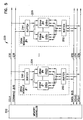
- a memory system which includes several DRAM devices per DRAM module is illustrated generally at 120 in Figure 3.
- Memory system 120 includes a memory controller 122 and N DRAM modules, such as indicated at 124 and 126.
- a command bus 128 is a unidirectional bus for carrying address and control information from memory controller 122 to the DRAM modules. Address and control information is typically transferred from memory controller 122 on command bus 128 in uniform packets on both rising and falling edges of a free-running clock (CCLK) provided on a clock line 130 from memory controller 122.
- CCLK free-running clock
- Data busses 132a-m are bidirectional busses carrying write data from memory controller 122 to the DRAM modules and further carrying read data from the DRAM modules to memory controller 122.
- Two bidirectional data clocks, DCLK0 and DCLK1 are respectively provided on clock lines 34a-m and clock lines 36a-m.
- DRAM module 124 includes a command buffer 140 for buffering commands from command bus 128 to be provided to M DRAM devices such as indicated at 142a and 142m.
- the Nth DRAM module indicated at 126 includes a command buffer 144 which buffers commands from command bus 128 to M DRAM devices such as indicated at 146a and 146m.
- memory system 120 does not include data buffers in the DRAM modules. Therefore memory system 20 includes M parallel data buses such as indicated at 132a and 132m. Corresponding data clocks are provided on 2M clock lines such as indicated at 134a and 134m for carrying DCLK0 and at 136a and 136m for carrying DCLK1. Memory system 120 is useful for memory applications requiring wider data buses for higher bandwidth, and yet not requiring command bus 128 to be duplicated for each data bus.
- Figure 4 is a timing diagram illustrating bus timing for memory system 120. Again, as in Figure 2, a sequence of four T read and write burst operations are illustrated in Figure 3.
- the command buffers such as indicated at 140 and 144 add an additional 2 T delay to get the command to the DRAM devices in the DRAM modules.
- the internal read operation starts at 19 T.
- the vernier clock adjustment in the DRAM module is adjusted so that output read0 data is provided at 29 T to the corresponding data bus and the output data read0 correspondingly arrives at memory controller 122 at time 30 T.
- write data is provided at time 36 T, and arrives at the DRAM module at time 37 T to permit the internal write operation to be performed at 41 T similar to the write timing of memory system 20.
- Memory system 220 includes a memory controller 222 and N DRAM modules, such as indicated at 224 and 226.
- a command bus 228 is a unidirectional bus for carrying address and control information from memory controller 222 to the DRAM modules. Address and control information is typically transferred from memory controller 222 on command bus 228 in uniform packets on both rising and falling edges of a free-running clock (CCLK) provided on a clock line 230 from memory controller 222.
- a data bus 232 is a bidirectional bus carrying write data from memory controller 222 to the DRAM modules and further carrying read data from the DRAM modules to memory controller 222. Two bidirectional data clocks, DCLK0 and DCLK1, are respectively provided on clock line 234 and clock line 236.
- the first DRAM module 224 includes a command buffer 240 which buffers commands to M DRAM devices, such as indicated at 242a and 242m.
- DRAM module 224 includes a data buffer 250 for buffering read and write data to be provided from and to the N DRAM devices 242a-m.
- the Nth DRAM module 226 includes a command buffer 224 for buffering commands to M DRAM devices, such as indicated at 246a and 246m.
- DRAM module 226 includes a data buffer 252 for buffering read and write data from and to the M DRAM devices 246a-m.
- data buffers such as data buffer 250 and data buffer 252, send and receive data from data bus 232 and send and receive the DCLK0 clock signal from clock line 234 and the DCLK1 clock signal from clock line 236.
- a memory system according to the present invention may actually include: one or more DRAM modules which include no command buffers and no data buffers; one or more DRAM modules which include command buffers but no data buffers; and one or more DRAM modules which include both command buffers and data buffers. Whether a particular DRAM module includes buffers or partial buffers is completely transparent to the memory controller of the memory system according to the present invention.
- Figure 6 illustrates, in timing diagram form, the bus timing for memory system 220.
- the data buffers such as data buffers 250 and 252 add an additional 2 T delay to read data.
- the internal read operation still begins at time 19 T, just as in memory system 120.
- the vernier clock adjustment circuitry in the DRAM module is adjusted to provide output data to data bus 232 at the DRAM module at time 27 T to assure arrival of the output data to memory controller 222 at time 30 T (i.e., 27 T plus 2 T delay from the data buffer plus the 1 T propagation delay on data bus 232).
- the read0 data arrives at the memory controller at 30 T whether or not command buffers and whether or not data buffers are used in the memory system.
- the write1 operation provides write1 data at time 36 T at memory controller 222, similar to the write1 operations illustrated in Figures 2 and 4 for memory systems 20 and 120.
- the write1 data arrives at the DRAM module at time 39 T instead of 37 T.
- the internal write 1 operation is performed beginning at time 43 T in memory system 220 instead of at time 41 T.
- memory controller 22 includes a command register 50 for providing commands to command bus 28 and a CCLK register 52 for providing the CCLK to clock line 30.
- a master clock is provided on a line 54 to registers 50 and 52.
- a write data register 56 is also clocked by the master clock on line 54 and provides write data to data bus 32.
- a read data register 58 receives read data from data bus 32 and receives its clock from an optional vernier clock adjustment circuit 60.
- Vernier clock adjustment circuit 60 receives the master clock from line 54 and the active one of the data clocks DCLK0 or DCLK1 via a register multiplexer 62, which receives DCLK0 and DCLK1 from clock lines 34 and 36.
- DRAM module 24 includes a command latch 64 which receives commands from command bus 28.
- Command latch 64 receives a delayed CCLK clock from a command vernier clock adjustment circuit 66.
- Command vernier clock adjustment circuit 66 receives the CCLK clock signal from clock line 30.
- a write first-in, first-out (FIFO) buffer 68 receives the DCLK0 and DCLK1 clock signals from lines 34 and 36 and the write data from data bus 32 and provides write data to a DRAM core 76.
- Write FIFO buffer 68 receives a. delayed CCLK clock from a write vernier clock adjustment circuit 70.
- Write vernier clock adjustment circuit 70 also receives the CCLK clock signal from clock line 30.
- a read FIFO buffer 72 receives read data from DRAM core 76 and provides the read data to data bus 32 along with the DCLK0 and DCLK1 clock signals to clock lines 34 and 36.
- Read FIFO buffer 72 receives a delayed CCLK clock from a read vernier clock adjustment circuit 74.
- Read vernier clock adjustment circuit 74 also receives the CCLK clock signal from clock line 30.
- DRAM devices from different suppliers manufactured at different points in a process spread, operating at different temperatures and supply voltages, and occupying different positions along the command bus and data bus, and operating with and without command buffers and/or data buffers necessarily comprise a range of loop-around delays from the read command provided on command bus 28 at memory controller 22 to input read data to memory controller 22 at the memory controller on data bus 32. Similar variations occur in write data having a range of loop-around delays from the write command at memory controller 22 to write data to the selected DRAM device from data bus 32.
- each DRAM includes a variety of vernier adjustment circuits which compensate for all of these variables to permit read data from all DRAMs to arrive at memory controller 22 within fixed, deterministic timing, and similarly permit write data to arrive with fixed, deterministic timing to the selected DRAM devices.
- the adjustments to vernier clock adjustment circuit 66, 70, 74 in each DRAM device is made by writing a delay value in a register located in each DRAM device.
- the delay typically includes a coarse adjustment setting providing a number of bit periods of delay adjustment, and a fine adjustment including a fine step to cover adjustment within a single bit.
- Vernier adjustment circuits 66, 70, 74, and 60 are typically implemented with tapped delay lines.
- inverters are staged and various tapped points along the tapped delay lines provide the required variations in vernier adjustment delays.
- the vernier delays are optionally provided with phase-lock loop (PLL) or delayed-lock loop (DLL) circuitry where various phases are selected from different places to provide the required variations in vernier adjustment delays.
- PLL phase-lock loop
- DLL delayed-lock loop
- the vernier clock adjustment circuits can be implemented in any suitable programmable delay elements.
- memory system 20 runs through all delay steps of the vernier circuit and determines when data misses on low adjustments and on high adjustments and sets the vernier adjustment in an approximated optimal middle setting.
- Another embodiment of memory system 20 includes a feedback controller used to set the vernier settings by first selecting an estimated optimal setting and allowing the controller and feedback circuitry to arrive at the optimal delay setting for the vernier clock adjustment circuit.
- memory controller 22 sends commands to the first DRAM module 24 and the command clock adjustment circuit 66 in DRAM module 24 is adjusted to optimally receive the command at command latch 64 from the command bus 28. Then memory controller 22 starts a write command sequence and the write vernier adjustment circuit 70 in DRAM module 24 is adjusted to permit optimal receiving of the write data at write FIFO buffer 68 from data bus 32. Next, a read command sequence is started by memory controller 22 and the read vernier clock adjustment circuit 74 is adjusted to permit optimal receiving of read data at read data register 58 from data bus 32.
- the command, write, and read vernier clock adjustment circuits are correspondingly adjusted with the above sequence of steps for each of the DRAM modules through the Nth DRAM module 26. Upon completion of these sequences, alignments of clocks, commands, write data bursts, and read data bursts from all sources are optimally adjusted.
- the read vernier delay is set to a minimum value in each of the DRAM devices.
- memory controller circuit 22 sends out write data on data bus 32 and attempts to receive the write data at read data register 58.
- memory controller 22 adjusts memory controller vernier clock adjustment circuit 60 to the optimal sampling instant. This adjustment establishes a read data timing reference point for ensuring timing alignment between write data bursts and read data bursts on data bus 32.
- Memory controller 22 then sends read data instructions to the first DRAM module 24 and observes the corresponding DCLK pattern returning on the data clock line 34 or 36. Memory controller 22 then writes the vernier delay control register of read vernier clock adjustment circuit 74 or otherwise sets the delay of the read vernier clock adjustment circuit to increase the delay until read delay data can be optimally sampled by the same internal memory controller clock timing that was used to read and write data in the previous step.
- Memory controller 22 correspondingly adjusts the read vernier clock adjustment circuits of each of the DRAM modules through the Nth DRAM module 26. Upon completion of this sequence, read data burst alignments from all sources are optimally adjusted.
- a constant delay from a command packet being provided on command bus 28 at memory controller 22 to read data or write data bursts at memory controller data bus I/O pins is established.
- one of DCLK0 or DCLK1 clocks is selected in vernier clock adjustment circuit 60 to latch the read data in read data register 58 instead of the master clock from line 54.
- Vernier circuit 60 of memory controller 22 can, however, be used periodically to monitor the timing of data from all sources and update DRAM vernier control registers as necessary to compensate for system timing drift.
- edges of CCLK clock and the DCLK clocks are coincident with data transitions on the command bus 28 and the data bus 32, respectively.
- the CCLK clock and the DCLK clocks are typically delayed by one-half of a bit period with the vernier clock adjustment circuits to optimally sample incoming data.
- the free-running CCLK is used to drive all internal DRAM timing.
- a delayed version of the CCLK is used to latch the command packets with vernier clock adjustment circuit 66.
- vernier adjustment circuits 70 and 74 provide delayed versions of the free-running CCLK clock to respectively clock the write FIFO buffer 68 and the read FIFO buffer 72.
- CMOS complementary metal-oxide-semiconductor
- CMOS complementary metal-oxide-semiconductor
- CMOS complementary metal-oxide-semiconductor
- CMOS complementary metal-oxide-semiconductor
- I Gbps I Gbps
- 1.2 Gbps 1.2 Gbps per pin
- the CCLK is 200 MHz or 2.5 N between each edge of the clock which is allocated as follows:
- FIG. 8A an ideal signal waveform is indicated at 80 having data valid between the times indicated between arrows 82. As illustrated in Figure 8A, ideal signal waveform 80 forms a big eye pattern.
- Figure 8B a non-ideal waveform is indicated at 84, which has a significantly reduced valid data period indicated by arrows 86.
- the non-ideal waveform 84 is produced as a result of jitter, skew, noise, overshoot, ringing and other such known problems.
- a second tier of vernier adjustment is added according to the present invention to the vernier adjustment circuitry in each DRAM module to individually adjust both a clock's falling-edge timing independent of or interdependent on the clock's rising edge.
- Vernier clock adjustment system 300 includes a rising-edge vernier adjustment circuit 302 and a falling-edge vernier adjustment circuit 304.
- a clock signal (CLK) is provided to the vernier adjustment circuits 302 and 304 on a clock line 306.
- Vernier clock adjustment circuit 302 independently delays the CLK signal from clock line 306 to provide a delayed version of the CLK signal on a clock line 308.
- the delayed clock on clock line 308 is used for rising-edge clockings.
- Falling-edge vernier clock adjustment circuit 304 independently delays the CLK signal from clock line 306 to provide a delayed version of the CLK signal on a clock line 310.
- the delayed clock signal on line 310 is used for falling-edge clockings.
- vernier clock adjustment system 300 includes two completely separate vernier circuits, one for independently delaying each clock edge.
- Vernier clock adjustment system 400 includes cascaded vernier clock adjustment circuits 402 and 404.
- a CLK signal is provided on a line 406 to vernier clock circuit 402.
- Vernier clock circuit 402 provides a delayed version of the CLK signal on a clock line 408.
- the delayed clock on line 408 is used for rising-edge clockings.
- Vernier clock adjustment circuit 402 also provides the same delayed version of the CLK signal to the second vernier clock adjustment circuit 404 via a line 409.
- Vernier clock adjustment circuit 404 further delays the clock signal to provide a delayed clock signal on a clock line 410.
- the delayed clock signal on line 410 is in used for falling-edge clockings.
- the falling-edge timing is based upon the rising-edge timing.
- An alternative embodiment (not shown) of the vernier clock adjustment system 400 is configured to make the rising edge timing be based on the falling edge timing.
- Vernier clock adjustment systems 300 and 400 are preferably employed in command vernier clock adjustment circuit 66, write vernier clock adjustment circuit 70, and read vernier clock adjustment circuit 74 of DRAM module 24 and the other DRAM modules of memory systems 20/120/220, such as illustrated in Figure 7.
- vernier adjustment circuit 60 of the memory controller 22 also includes such individual edge adjustment as provided by either vernier clock system 300 or 400.
- rising-edge clock data is first adjusted, followed by falling-edge clock data.
- the rising-edge clock data is adjusted by adjusting the delay provided by the rising-edge vernier adjustment circuit 302 of system 300 or circuit 402 of system 400.
- the falling-edge clock data is then adjusted by adjusting the delay of falling-edge vernier adjustment circuit 304 of system 300 or circuit 404 of system 400.
- Alternate embodiments of memory system 20/120/220 first adjust the falling-edge time followed by the rising edge timing during system initialization.
- the falling-edge and rising-edge adjustments provided by vernier clock adjustment systems 300 and 400 are especially beneficial to lessen memory system demands upon clock duty cycle.
- the echo clock scheme employed for producing DCLK0 and DCLK1 in the memory systems 20, 120, and 220 is especially vulnerable to duty cycle problems since each DRAM device must receive a clock and retransmit the clock with the read data. Each time the clock is converted to and from the data bus, the duty cycle is affected.
- the memory system according to the present invention compensates for these duty cycle problems by employing the clock verniers to individually adjust both the rising and falling edges of the clock.
- a memory system such as memory system 20, 120, or 220, typically operates on an industry standard protocol where the DRAM devices, whether or not manufactured from different suppliers, look the same to the memory controller.
- the DRAM devices may be at different points in the process spread, such as at 400 Mbps as compared to 800 Mbps.
- DRAM devices may be operating at different temperatures and supply voltages and be occupying different positions along the command bus and data bus, and at the same time the DRAM devices can be with and without command buffers and data buffers. The more precise adjustment of adjusting both falling and rising edge of the clocks better compensates for these problems.
- the vernier clock adjustment circuitry and method according to the present invention in memory systems, such as memory systems 20/120/220, the effects of duty cycle variation, bus position of a given memory device, timing drift, loading variations, clock jitter, clock skew, noise, overshoot, and ringing are more accurately and precisely compensated for by individually adjusting both the rising-edge and falling-edge timings interdependently from each other. In this way, data can be accurately clocked in the memory devices even at higher data transmission rates.
Abstract
Description
Claims (16)
- An integrated circuit (20; 120; 220) comprising:a vernier clock adjustment circuit (66, 70, 74) receiving an input clock signal (CLK) including a rising-edge delay circuit receiving the input clock signal (CLK) and providing a rising-edge clock signal representing the input clock signal (CLK) delayed by a rising-edge delay, the vernier clock adjustment circuit (66, 70, 74) further including a falling-edge delay circuit (404) receiving the rising-edge clock signal and providing a falling-edge clock signal representing the input clock signal (CLK) delayed by a falling-edge delay; andan edge triggered circuit (64, 68, 72) receiving data and the rising-edge and falling-edge clock signals, and storing data at the rising-edge of the rising-edge clock signal and at the falling-edge of the falling-edge clock signal.
- The integrated circuit of claim 1 wherein the rising-edge and falling-edge delays comprise programmable delays.
- The integrated circuit of claim 1 wherein the integrated circuit comprises a memory integrated circuit (20; 120; 220).
- An integrated circuit comprising:a vernier clock adjustment circuit (66, 70, 74) receiving an input clock signal including a falling-edge delay circuit receiving the input clock signal and providing a falling-edge clock signal representing the input clock signal (CLK) delayed by a falling-edge delay, the vernier clock-adjustment circuit (66, 70, 74) further including a rising-edge delay circuit receiving the falling-edge clock signal and providing a rising-edge clock signal representing the input clock signal delayed by a rising-edge delay; andan edge triggered circuit (64, 68, 72) receiving data and the rising-edge and falling-edge clock signals, and storing data at the rising-edge of the rising-edge clock signal and at the falling-edge of the falling-edge clock signal.
- The integrated circuit (20; 120; 220) of claim 4 wherein the rising-edge and falling-edge delays comprise programmable delays.
- The integrated circuit of claim 4 wherein the integrated circuit comprises a memory integrated circuit (20; 120; 220).
- A method of operating in an integrated circuit comprising the steps of:receiving an input clock signal (CLK);delaying the input clock signal to provide a rising-edge clock signal representing the input clock signal (CLK) delayed by a rising-edge delay:delaying the rising-edge clock signal to provide a falling-edge clock signal representing the input clock signal delayed by a falling-edge delay; andstoring data at the rising-edge of the rising-edge clock signal and at the falling-edge of the falling-edge clock signal.
- The method of claim 7 further comprising:programming the rising-edge and falling-edge delays.
- A method of operating in an integrated circuit comprising the steps of:receiving an input clock signal (CLK);delaying the input clock signal (CLK) to provide a falling-edge clock signal representing the input clock signal delayed by a falling-edge delay;delaying the falling-edge clock signal to provide a rising-edge clock signal representing the input clock signal delayed by a rising-edge delay; andstoring data at the rising-edge of the rising-edge clock signal and at the falling-edge of the falling-edge clock signal.
- The method of claim 9 further comprising:programming the rising-edge and falling-edge delays.
- A memory system (20; 120; 220) comprising:a memory controller (22; 122; 222),a plurality of memory modules (24, 26; 124, 126; 224, 226) for storing data;a data bus (32; 132; 232) for carrying write data from the memory controller (22; 122; 222) to the plurality of memory modules and for carrying read data from the plurality of memory modules (24, 26; 124, 126; 224, 226) to the memory controller (22; 122; 222);a command bus (28; 128; 238) carrying commands from the memory controller (22; 122; 222) to the plurality of memory modules (24, 26; 124, 126; 224, 226);a clock line (30; 130; 230) for carrying an input clock signal from the memory controller (22; 122; 222) to the plurality of memory modules (24, 26; 124, 126; 224, 226); andwherein each memory module includes:a vernier clock adjustment circuit (66, 70, 74) including a rising-edge delay circuit (402) receiving the input clock signal and providing a rising-edge clock signal representing the input clock signal delayed by a rising-edge delay, the vernier clock adjustment circuit further including a falling-edge delay circuit (404) receiving the rising-edge clock signal and providing a falling-edge clock signal representing the input clock signal delayed by a falling-edge delay; andan edge triggered circuit (64, 68, 72) receiving data and the rising-edge and falling-edge clock signals, and storing data at the rising-edge of the rising-edge clock signal and at the falling-edge of the falling-edge clock signal.
- The memory system of claim 11 wherein the memory controller (22; 122; 222) programs the rising-edge and falling-edge delays by sending command to the plurality of memory modules (24, 26; 124, 126; 224, 226).
- The memory system of claim 11 wherein the plurality of memory modules (24, 26; 124, 126; 224, 226) each include at least one dynamic random access memory (142a..m; 146a..m; 76).
- A memory system (20; 120; 220) comprising:a memory controller (22; 122; 222);a plurality of memory modules (24, 26; 124, 126; 224, 226) for storing data;a data bus (32; 132; 232) for carrying write data from the memory controller (22; 122; 222) to the plurality of memory modules and for carrying read data from the plurality of memory modules to the memory controller (22; 122; 222);a command bus (28; 128; 238) carrying commands from the memory controller to the plurality of memory modules (24, 26; 124, 126; 224 226);a clock line (30; 130; 230) for carrying an input clock signal from the memory controller (22; 122; 222) to the plurality of memory modules; andwherein each memory module includes:a vernier clock adjustment circuit (66, 70, 74) including a falling-edge delay circuit receiving the input clock signal and providing a falling-edge clock signal representing the input clock signal delayed by a falling-edge delay, the vernier clock adjustment circuit further including a rising-edge delay circuit receiving the falling-edge clock signal and providing a rising-edge clock signal representing the input clock signal delayed by a rising-edge delay; andan edge triggered circuit (64, 68, 72) receiving data and the rising-edge and falling-edge clock signals, and storing data at the rising-edge of the rising-edge clock signal and at the falling-edge of the falling-edge clock signal.
- The memory system of claim 14 wherein the memory controller (22; 122; 222) programs the rising-edge and falling-edge delays by sending command to the plurality of memory modules.
- The memory system of claim 14 wherein the plurality of memory modules (24, 26; 124, 126; 224, 226) each include at least one dynamic random access memory (142a..m; 146a..m; 76).
Applications Claiming Priority (3)
| Application Number | Priority Date | Filing Date | Title |
|---|---|---|---|
| US08/759,351 US6115318A (en) | 1996-12-03 | 1996-12-03 | Clock vernier adjustment |
| US759351 | 1996-12-03 | ||
| PCT/US1997/022001 WO1998025345A1 (en) | 1996-12-03 | 1997-12-03 | Clock vernier adjustment |
Publications (2)
| Publication Number | Publication Date |
|---|---|
| EP0943177A1 EP0943177A1 (en) | 1999-09-22 |
| EP0943177B1 true EP0943177B1 (en) | 2002-10-02 |
Family
ID=25055332
Family Applications (1)
| Application Number | Title | Priority Date | Filing Date |
|---|---|---|---|
| EP97951512A Expired - Lifetime EP0943177B1 (en) | 1996-12-03 | 1997-12-03 | Clock vernier adjustment |
Country Status (8)
| Country | Link |
|---|---|
| US (1) | US6115318A (en) |
| EP (1) | EP0943177B1 (en) |
| JP (1) | JP2001505693A (en) |
| KR (1) | KR100435612B1 (en) |
| AT (1) | ATE225581T1 (en) |
| AU (1) | AU5513998A (en) |
| DE (1) | DE69716112T2 (en) |
| WO (1) | WO1998025345A1 (en) |
Families Citing this family (50)
| Publication number | Priority date | Publication date | Assignee | Title |
|---|---|---|---|---|
| US6088774A (en) * | 1996-09-20 | 2000-07-11 | Advanced Memory International, Inc. | Read/write timing for maximum utilization of bidirectional read/write bus |
| US6173432B1 (en) | 1997-06-20 | 2001-01-09 | Micron Technology, Inc. | Method and apparatus for generating a sequence of clock signals |
| US6101197A (en) * | 1997-09-18 | 2000-08-08 | Micron Technology, Inc. | Method and apparatus for adjusting the timing of signals over fine and coarse ranges |
| US6067594A (en) * | 1997-09-26 | 2000-05-23 | Rambus, Inc. | High frequency bus system |
| US6401167B1 (en) | 1997-10-10 | 2002-06-04 | Rambus Incorporated | High performance cost optimized memory |
| JP3259764B2 (en) * | 1997-11-28 | 2002-02-25 | 日本電気株式会社 | Semiconductor storage device |
| US6330627B1 (en) | 1998-01-20 | 2001-12-11 | Kabushiki Kaisha Toshiba | System for fast data transfer between memory modules and controller using two clock lines each having a go line portion and a return line portion |
| JPH11328961A (en) * | 1998-05-21 | 1999-11-30 | Fujitsu Ltd | Electronic circuit device and interface circuit |
| US6349399B1 (en) | 1998-09-03 | 2002-02-19 | Micron Technology, Inc. | Method and apparatus for generating expect data from a captured bit pattern, and memory device using same |
| US6470060B1 (en) | 1999-03-01 | 2002-10-22 | Micron Technology, Inc. | Method and apparatus for generating a phase dependent control signal |
| KR100301054B1 (en) * | 1999-04-07 | 2001-10-29 | 윤종용 | Semiconductor memory device increasing transfer data rate of data input/output bus and memory module having the same |
| KR100318264B1 (en) * | 1999-06-28 | 2001-12-24 | 박종섭 | load signal generation circuit in packet command driving type memory device |
| US6446180B2 (en) * | 1999-07-19 | 2002-09-03 | Micron Technology, Inc. | Memory device with synchronized output path |
| US6643787B1 (en) | 1999-10-19 | 2003-11-04 | Rambus Inc. | Bus system optimization |
| US6646953B1 (en) | 2000-07-06 | 2003-11-11 | Rambus Inc. | Single-clock, strobeless signaling system |
| US6629251B1 (en) * | 1999-10-20 | 2003-09-30 | Applied Micro Circuits Corporation | Elastic store circuit with vernier clock delay |
| US6681272B1 (en) * | 1999-10-20 | 2004-01-20 | Applied Micro Circuits Corporation | Elastic store circuit with static phase offset |
| JP4675442B2 (en) * | 1999-11-02 | 2011-04-20 | 富士通セミコンダクター株式会社 | Memory device |
| US6910146B2 (en) * | 1999-12-31 | 2005-06-21 | Intel Corporation | Method and apparatus for improving timing margin in an integrated circuit as determined from recorded pass/fail indications for relative phase settings |
| US6647507B1 (en) * | 1999-12-31 | 2003-11-11 | Intel Corporation | Method for improving a timing margin in an integrated circuit by setting a relative phase of receive/transmit and distributed clock signals |
| DE10004108C1 (en) * | 2000-01-31 | 2001-08-09 | Infineon Technologies Ag | Circuit for generating output clock signal with optimised signal generation time for memory arrangement eliminates certain problems related to transition times - has duty cycle equaliser with 2 coupled symmetrical branches contg. multiplexer integrated with programmable signal supply points producing output signal |
| JP2002082830A (en) * | 2000-02-14 | 2002-03-22 | Mitsubishi Electric Corp | Interface circuit |
| JP3757757B2 (en) * | 2000-05-18 | 2006-03-22 | 株式会社日立製作所 | Read priority memory system |
| US6807613B1 (en) * | 2000-08-21 | 2004-10-19 | Mircon Technology, Inc. | Synchronized write data on a high speed memory bus |
| JP4652562B2 (en) * | 2000-12-26 | 2011-03-16 | キヤノン株式会社 | Memory control device |
| US7313715B2 (en) * | 2001-02-09 | 2007-12-25 | Samsung Electronics Co., Ltd. | Memory system having stub bus configuration |
| US6747474B2 (en) * | 2001-02-28 | 2004-06-08 | Intel Corporation | Integrated circuit stubs in a point-to-point system |
| US6434082B1 (en) * | 2001-03-13 | 2002-08-13 | International Business Machines Corporation | Clocked memory device that includes a programming mechanism for setting write recovery time as a function of the input clock |
| US6675272B2 (en) | 2001-04-24 | 2004-01-06 | Rambus Inc. | Method and apparatus for coordinating memory operations among diversely-located memory components |
| US8391039B2 (en) | 2001-04-24 | 2013-03-05 | Rambus Inc. | Memory module with termination component |
| US6570813B2 (en) | 2001-05-25 | 2003-05-27 | Micron Technology, Inc. | Synchronous mirror delay with reduced delay line taps |
| JP2003044349A (en) * | 2001-07-30 | 2003-02-14 | Elpida Memory Inc | Register and signal generating method |
| JP4812976B2 (en) * | 2001-07-30 | 2011-11-09 | エルピーダメモリ株式会社 | Register, memory module and memory system |
| DE10149031A1 (en) * | 2001-10-05 | 2003-04-24 | Infineon Technologies Ag | Dynamic random access memory has read clock generator which is arranged in memory module, so that data bus and read clock bus are substantially symmetric |
| DE10154505B4 (en) * | 2001-11-07 | 2006-11-16 | Infineon Technologies Ag | Memory device and method for accessing a memory module |
| US7071749B2 (en) * | 2002-03-25 | 2006-07-04 | Aeroflex Colorado Springs Inc. | Error correcting latch |
| JP4159415B2 (en) | 2002-08-23 | 2008-10-01 | エルピーダメモリ株式会社 | Memory module and memory system |
| US6920187B2 (en) | 2002-10-02 | 2005-07-19 | Micron Technology, Inc. | Constant delay zero standby differential logic receiver and method |
| US7234099B2 (en) * | 2003-04-14 | 2007-06-19 | International Business Machines Corporation | High reliability memory module with a fault tolerant address and command bus |
| US7168027B2 (en) | 2003-06-12 | 2007-01-23 | Micron Technology, Inc. | Dynamic synchronization of data capture on an optical or other high speed communications link |
| US7233185B2 (en) * | 2003-10-10 | 2007-06-19 | Atmel Corporation | Vernier circuit for fine control of sample time |
| JP2005267713A (en) * | 2004-03-17 | 2005-09-29 | Toshiba Corp | Dynamic type semiconductor memory device |
| US7301831B2 (en) | 2004-09-15 | 2007-11-27 | Rambus Inc. | Memory systems with variable delays for write data signals |
| US7542322B2 (en) * | 2004-09-30 | 2009-06-02 | Intel Corporation | Buffered continuous multi-drop clock ring |
| KR100892647B1 (en) * | 2007-08-13 | 2009-04-09 | 주식회사 하이닉스반도체 | Circuit for Generating Clock of Semiconductor Memory Apparatus |
| KR101470975B1 (en) * | 2007-12-21 | 2014-12-09 | 램버스 인코포레이티드 | Method and apparatus for calibrating write timing in a memory system |
| JP5268392B2 (en) * | 2008-03-07 | 2013-08-21 | パナソニック株式会社 | Memory device, memory system, and access timing adjustment method in memory system |
| JP2009237678A (en) * | 2008-03-26 | 2009-10-15 | Fujitsu Microelectronics Ltd | Memory controller device, control method for memory controller device and data reception device |
| DE102012222357A1 (en) * | 2012-12-05 | 2014-06-05 | Robert Bosch Gmbh | Inter-Integrated Circuit Slave Interface and Method of Operating an Integrated Integrated Circuit Slave Interface |
| US20230244264A1 (en) * | 2022-01-31 | 2023-08-03 | Nvidia Corporation | Fast Clock Detection |
Family Cites Families (116)
| Publication number | Priority date | Publication date | Assignee | Title |
|---|---|---|---|---|
| US3633174A (en) * | 1970-04-14 | 1972-01-04 | Us Navy | Memory system having self-adjusting strobe timing |
| US4096402A (en) * | 1975-12-29 | 1978-06-20 | Mostek Corporation | MOSFET buffer for TTL logic input and method of operation |
| US4077016A (en) * | 1977-02-22 | 1978-02-28 | Ncr Corporation | Apparatus and method for inhibiting false locking of a phase-locked loop |
| US4404474A (en) * | 1981-02-06 | 1983-09-13 | Rca Corporation | Active load pulse generating circuit |
| US4481625A (en) * | 1981-10-21 | 1984-11-06 | Elxsi | High speed data bus system |
| US4511846A (en) * | 1982-05-24 | 1985-04-16 | Fairchild Camera And Instrument Corporation | Deskewing time-critical signals in automatic test equipment |
| US4514647A (en) * | 1983-08-01 | 1985-04-30 | At&T Bell Laboratories | Chipset synchronization arrangement |
| US4687951A (en) * | 1984-10-29 | 1987-08-18 | Texas Instruments Incorporated | Fuse link for varying chip operating parameters |
| US4600895A (en) * | 1985-04-26 | 1986-07-15 | Minnesota Mining And Manufacturing Company | Precision phase synchronization of free-running oscillator output signal to reference signal |
| US4638187A (en) * | 1985-10-01 | 1987-01-20 | Vtc Incorporated | CMOS output buffer providing high drive current with minimum output signal distortion |
| GB2184622B (en) * | 1985-12-23 | 1989-10-18 | Philips Nv | Outputbuffer and control circuit providing limited current rate at the output |
| US4773085A (en) * | 1987-06-12 | 1988-09-20 | Bell Communications Research, Inc. | Phase and frequency detector circuits |
| US5086500A (en) * | 1987-08-07 | 1992-02-04 | Tektronix, Inc. | Synchronized system by adjusting independently clock signals arriving at a plurality of integrated circuits |
| DE3855492T2 (en) * | 1987-08-07 | 1997-01-09 | Tektronix Inc | High-speed computer with a limited instruction set, which is divided into several circuits |
| US4893087A (en) * | 1988-01-07 | 1990-01-09 | Motorola, Inc. | Low voltage and low power frequency synthesizer |
| KR0141494B1 (en) * | 1988-01-28 | 1998-07-15 | 미다 가쓰시게 | High speed sensor system using a level shift circuit |
| US4902986B1 (en) * | 1989-01-30 | 1998-09-01 | Credence Systems Corp | Phased locked loop to provide precise frequency and phase tracking of two signals |
| US5020023A (en) * | 1989-02-23 | 1991-05-28 | International Business Machines Corporation | Automatic vernier synchronization of skewed data streams |
| US4958088A (en) * | 1989-06-19 | 1990-09-18 | Micron Technology, Inc. | Low power three-stage CMOS input buffer with controlled switching |
| IT1236578B (en) | 1989-07-04 | 1993-03-16 | Ind Face Standard S P A Milano | Type D flip=flop to type B flip=flop converter circuit |
| US5165046A (en) * | 1989-11-06 | 1992-11-17 | Micron Technology, Inc. | High speed CMOS driver circuit |
| JP2671538B2 (en) * | 1990-01-17 | 1997-10-29 | 松下電器産業株式会社 | Input buffer circuit |
| JP2787725B2 (en) * | 1990-02-14 | 1998-08-20 | 第一電子工業株式会社 | Data clock timing adjustment circuit |
| US5408640A (en) * | 1990-02-21 | 1995-04-18 | Digital Equipment Corporation | Phase delay compensator using gating signal generated by a synchronizer for loading and shifting of bit pattern to produce clock phases corresponding to frequency changes |
| US5239206A (en) * | 1990-03-06 | 1993-08-24 | Advanced Micro Devices, Inc. | Synchronous circuit with clock skew compensating function and circuits utilizing same |
| US5023488A (en) | 1990-03-30 | 1991-06-11 | Xerox Corporation | Drivers and receivers for interfacing VLSI CMOS circuits to transmission lines |
| IL96808A (en) * | 1990-04-18 | 1996-03-31 | Rambus Inc | Integrated circuit i/o using a high performance bus interface |
| US5243703A (en) * | 1990-04-18 | 1993-09-07 | Rambus, Inc. | Apparatus for synchronously generating clock signals in a data processing system |
| US5038115A (en) * | 1990-05-29 | 1991-08-06 | Myers Glen A | Method and apparatus for frequency independent phase tracking of input signals in receiving systems and the like |
| US5134311A (en) * | 1990-06-07 | 1992-07-28 | International Business Machines Corporation | Self-adjusting impedance matching driver |
| US5122690A (en) * | 1990-10-16 | 1992-06-16 | General Electric Company | Interface circuits including driver circuits with switching noise reduction |
| US5257294A (en) * | 1990-11-13 | 1993-10-26 | National Semiconductor Corporation | Phase-locked loop circuit and method |
| TW198135B (en) * | 1990-11-20 | 1993-01-11 | Oki Electric Ind Co Ltd | |
| US5128563A (en) * | 1990-11-28 | 1992-07-07 | Micron Technology, Inc. | CMOS bootstrapped output driver method and circuit |
| US5281865A (en) * | 1990-11-28 | 1994-01-25 | Hitachi, Ltd. | Flip-flop circuit |
| US5150186A (en) * | 1991-03-06 | 1992-09-22 | Micron Technology, Inc. | CMOS output pull-up driver |
| US5128560A (en) * | 1991-03-22 | 1992-07-07 | Micron Technology, Inc. | Boosted supply output driver circuit for driving an all N-channel output stage |
| US5220208A (en) * | 1991-04-29 | 1993-06-15 | Texas Instruments Incorporated | Circuitry and method for controlling current in an electronic circuit |
| US5212601A (en) * | 1991-05-03 | 1993-05-18 | Western Digital Corporation | Disk drive data synchronizer with window shift synthesis |
| US5256989A (en) * | 1991-05-03 | 1993-10-26 | Motorola, Inc. | Lock detection for a phase lock loop |
| US5194765A (en) * | 1991-06-28 | 1993-03-16 | At&T Bell Laboratories | Digitally controlled element sizing |
| US5276642A (en) * | 1991-07-15 | 1994-01-04 | Micron Technology, Inc. | Method for performing a split read/write operation in a dynamic random access memory |
| KR970005124B1 (en) * | 1991-08-14 | 1997-04-12 | 가부시끼가이샤 아드반테스트 | Variable delayed circuit |
| US5465076A (en) * | 1991-10-04 | 1995-11-07 | Nippondenso Co., Ltd. | Programmable delay line programmable delay circuit and digital controlled oscillator |
| US5283631A (en) * | 1991-11-01 | 1994-02-01 | Hewlett-Packard Co. | Programmable capacitance delay element having inverters controlled by adjustable voltage to offset temperature and voltage supply variations |
| US5498990A (en) * | 1991-11-05 | 1996-03-12 | Monolithic System Technology, Inc. | Reduced CMOS-swing clamping circuit for bus lines |
| US5295164A (en) * | 1991-12-23 | 1994-03-15 | Apple Computer, Inc. | Apparatus for providing a system clock locked to an external clock over a wide range of frequencies |
| DE4206082C1 (en) * | 1992-02-27 | 1993-04-08 | Siemens Ag, 8000 Muenchen, De | |
| DE4345604B3 (en) * | 1992-03-06 | 2012-07-12 | Rambus Inc. | Device for communication with a DRAM |
| US5355391A (en) * | 1992-03-06 | 1994-10-11 | Rambus, Inc. | High speed bus system |
| US5278460A (en) * | 1992-04-07 | 1994-01-11 | Micron Technology, Inc. | Voltage compensating CMOS input buffer |
| US5390308A (en) * | 1992-04-15 | 1995-02-14 | Rambus, Inc. | Method and apparatus for address mapping of dynamic random access memory |
| US5254883A (en) * | 1992-04-22 | 1993-10-19 | Rambus, Inc. | Electrical current source circuitry for a bus |
| US5265218A (en) * | 1992-05-19 | 1993-11-23 | Sun Microsystems, Inc. | Bus architecture for integrated data and video memory |
| US5317202A (en) * | 1992-05-28 | 1994-05-31 | Intel Corporation | Delay line loop for 1X on-chip clock generation with zero skew and 50% duty cycle |
| US5485490A (en) * | 1992-05-28 | 1996-01-16 | Rambus, Inc. | Method and circuitry for clock synchronization |
| US5268639A (en) * | 1992-06-05 | 1993-12-07 | Rambus, Inc. | Testing timing parameters of high speed integrated circuit devices |
| US5274276A (en) * | 1992-06-26 | 1993-12-28 | Micron Technology, Inc. | Output driver circuit comprising a programmable circuit for determining the potential at the output node and the method of implementing the circuit |
| US5473274A (en) * | 1992-09-14 | 1995-12-05 | Nec America, Inc. | Local clock generator |
| FR2696061B1 (en) * | 1992-09-22 | 1994-12-02 | Rainard Jean Luc | Method for temporally delaying a signal and corresponding delay circuit. |
| EP0596657A3 (en) * | 1992-11-05 | 1994-12-07 | American Telephone & Telegraph | Normalization of apparent propagation delay. |
| US5311481A (en) * | 1992-12-17 | 1994-05-10 | Micron Technology, Inc. | Wordline driver circuit having a directly gated pull-down device |
| JP2792801B2 (en) * | 1992-12-28 | 1998-09-03 | 三菱電機株式会社 | Semiconductor integrated circuit, design method and manufacturing method thereof |
| US5347559A (en) * | 1992-12-30 | 1994-09-13 | Digital Equipment Corporation | Apparatus and method of data transfer between systems using different clocks |
| US5347177A (en) * | 1993-01-14 | 1994-09-13 | Lipp Robert J | System for interconnecting VLSI circuits with transmission line characteristics |
| US5544203A (en) * | 1993-02-17 | 1996-08-06 | Texas Instruments Incorporated | Fine resolution digital delay line with coarse and fine adjustment stages |
| JPH06273423A (en) | 1993-03-18 | 1994-09-30 | Daikin Ind Ltd | Method for shortening measuring hour of measuring apparatus |
| US5488321A (en) * | 1993-04-07 | 1996-01-30 | Rambus, Inc. | Static high speed comparator |
| US5347179A (en) * | 1993-04-15 | 1994-09-13 | Micron Semiconductor, Inc. | Inverting output driver circuit for reducing electron injection into the substrate |
| US5337285A (en) * | 1993-05-21 | 1994-08-09 | Rambus, Inc. | Method and apparatus for power control in devices |
| AU6988494A (en) * | 1993-05-28 | 1994-12-20 | Rambus Inc. | Method and apparatus for implementing refresh in a synchronous dram system |
| US5506814A (en) * | 1993-05-28 | 1996-04-09 | Micron Technology, Inc. | Video random access memory device and method implementing independent two WE nibble control |
| JP2636677B2 (en) * | 1993-06-02 | 1997-07-30 | 日本電気株式会社 | Semiconductor integrated circuit |
| US5511024A (en) * | 1993-06-02 | 1996-04-23 | Rambus, Inc. | Dynamic random access memory system |
| US5428311A (en) * | 1993-06-30 | 1995-06-27 | Sgs-Thomson Microelectronics, Inc. | Fuse circuitry to control the propagation delay of an IC |
| US5473639A (en) * | 1993-07-26 | 1995-12-05 | Hewlett-Packard Company | Clock recovery apparatus with means for sensing an out of lock condition |
| JP3232351B2 (en) * | 1993-10-06 | 2001-11-26 | 三菱電機株式会社 | Digital circuit device |
| US5451898A (en) * | 1993-11-12 | 1995-09-19 | Rambus, Inc. | Bias circuit and differential amplifier having stabilized output swing |
| JP3547466B2 (en) | 1993-11-29 | 2004-07-28 | 株式会社東芝 | Memory device, serial-parallel data conversion circuit, method for writing data to memory device, and serial-parallel data conversion method |
| JPH07153286A (en) * | 1993-11-30 | 1995-06-16 | Sony Corp | Non-volatile semiconductor memory |
| US5400283A (en) * | 1993-12-13 | 1995-03-21 | Micron Semiconductor, Inc. | RAM row decode circuitry that utilizes a precharge circuit that is deactivated by a feedback from an activated word line driver |
| KR0132504B1 (en) * | 1993-12-21 | 1998-10-01 | 문정환 | Data output buffer |
| US5579326A (en) * | 1994-01-31 | 1996-11-26 | Sgs-Thomson Microelectronics, Inc. | Method and apparatus for programming signal timing |
| KR100393317B1 (en) * | 1994-02-15 | 2003-10-23 | 람버스 인코포레이티드 | Delayed synchronization loop |
| US5424672A (en) * | 1994-02-24 | 1995-06-13 | Micron Semiconductor, Inc. | Low current redundancy fuse assembly |
| US5440514A (en) * | 1994-03-08 | 1995-08-08 | Motorola Inc. | Write control for a memory using a delay locked loop |
| US5554946A (en) * | 1994-04-08 | 1996-09-10 | International Business Machines Corporation | Timing signal generator |
| US5497115A (en) | 1994-04-29 | 1996-03-05 | Mosaid Technologies Incorporated | Flip-flop circuit having low standby power for driving synchronous dynamic random access memory |
| JP3553639B2 (en) * | 1994-05-12 | 2004-08-11 | アジレント・テクノロジーズ・インク | Timing adjustment circuit |
| US5457407A (en) * | 1994-07-06 | 1995-10-10 | Sony Electronics Inc. | Binary weighted reference circuit for a variable impedance output buffer |
| JP3537500B2 (en) | 1994-08-16 | 2004-06-14 | バー−ブラウン・コーポレーション | Inverter device |
| JP3176228B2 (en) * | 1994-08-23 | 2001-06-11 | シャープ株式会社 | Semiconductor storage device |
| GB9417266D0 (en) * | 1994-08-26 | 1994-10-19 | Inmos Ltd | Testing a non-volatile memory |
| JPH08139572A (en) * | 1994-11-07 | 1996-05-31 | Mitsubishi Electric Corp | Latch circuit |
| US5497127A (en) * | 1994-12-14 | 1996-03-05 | David Sarnoff Research Center, Inc. | Wide frequency range CMOS relaxation oscillator with variable hysteresis |
| US5577236A (en) * | 1994-12-30 | 1996-11-19 | International Business Machines Corporation | Memory controller for reading data from synchronous RAM |
| US5489864A (en) * | 1995-02-24 | 1996-02-06 | Intel Corporation | Delay interpolation circuitry |
| US5578940A (en) * | 1995-04-04 | 1996-11-26 | Rambus, Inc. | Modular bus with single or double parallel termination |
| US5621690A (en) * | 1995-04-28 | 1997-04-15 | Intel Corporation | Nonvolatile memory blocking architecture and redundancy |
| JP3386924B2 (en) | 1995-05-22 | 2003-03-17 | 株式会社日立製作所 | Semiconductor device |
| US5581197A (en) * | 1995-05-31 | 1996-12-03 | Hewlett-Packard Co. | Method of programming a desired source resistance for a driver stage |
| US5576645A (en) * | 1995-06-05 | 1996-11-19 | Hughes Aircraft Company | Sample and hold flip-flop for CMOS logic |
| US5636173A (en) | 1995-06-07 | 1997-06-03 | Micron Technology, Inc. | Auto-precharge during bank selection |
| JP3403551B2 (en) | 1995-07-14 | 2003-05-06 | 沖電気工業株式会社 | Clock distribution circuit |
| US5621340A (en) * | 1995-08-02 | 1997-04-15 | Rambus Inc. | Differential comparator for amplifying small swing signals to a full swing output |
| JP3252666B2 (en) | 1995-08-14 | 2002-02-04 | 日本電気株式会社 | Semiconductor storage device |
| US5578941A (en) * | 1995-08-23 | 1996-11-26 | Micron Technology, Inc. | Voltage compensating CMOS input buffer circuit |
| US5692165A (en) | 1995-09-12 | 1997-11-25 | Micron Electronics Inc. | Memory controller with low skew control signal |
| JP3408030B2 (en) | 1995-09-21 | 2003-05-19 | 日本プレシジョン・サーキッツ株式会社 | Phase comparator |
| US5594690A (en) * | 1995-12-15 | 1997-01-14 | Unisys Corporation | Integrated circuit memory having high speed and low power by selectively coupling compensation components to a pulse generator |
| US5636174A (en) | 1996-01-11 | 1997-06-03 | Cirrus Logic, Inc. | Fast cycle time-low latency dynamic random access memories and systems and methods using the same |
| US5719508A (en) | 1996-02-01 | 1998-02-17 | Northern Telecom, Ltd. | Loss of lock detector for master timing generator |
| US5712580A (en) | 1996-02-14 | 1998-01-27 | International Business Machines Corporation | Linear phase detector for half-speed quadrature clocking architecture |
| US5627791A (en) | 1996-02-16 | 1997-05-06 | Micron Technology, Inc. | Multiple bank memory with auto refresh to specified bank |
| US5668763A (en) | 1996-02-26 | 1997-09-16 | Fujitsu Limited | Semiconductor memory for increasing the number of half good memories by selecting and using good memory blocks |
| US5621739A (en) * | 1996-05-07 | 1997-04-15 | Intel Corporation | Method and apparatus for buffer self-test and characterization |
-
1996
- 1996-12-03 US US08/759,351 patent/US6115318A/en not_active Expired - Lifetime
-
1997
- 1997-12-03 DE DE69716112T patent/DE69716112T2/en not_active Expired - Lifetime
- 1997-12-03 JP JP52574298A patent/JP2001505693A/en active Pending
- 1997-12-03 AU AU55139/98A patent/AU5513998A/en not_active Abandoned
- 1997-12-03 AT AT97951512T patent/ATE225581T1/en not_active IP Right Cessation
- 1997-12-03 EP EP97951512A patent/EP0943177B1/en not_active Expired - Lifetime
- 1997-12-03 KR KR10-1999-7004924A patent/KR100435612B1/en not_active IP Right Cessation
- 1997-12-03 WO PCT/US1997/022001 patent/WO1998025345A1/en active IP Right Grant
Also Published As
| Publication number | Publication date |
|---|---|
| DE69716112T2 (en) | 2003-05-28 |
| KR20000069287A (en) | 2000-11-25 |
| ATE225581T1 (en) | 2002-10-15 |
| WO1998025345A1 (en) | 1998-06-11 |
| JP2001505693A (en) | 2001-04-24 |
| DE69716112D1 (en) | 2002-11-07 |
| KR100435612B1 (en) | 2004-06-12 |
| EP0943177A1 (en) | 1999-09-22 |
| AU5513998A (en) | 1998-06-29 |
| US6115318A (en) | 2000-09-05 |
Similar Documents
| Publication | Publication Date | Title |
|---|---|---|
| EP0943177B1 (en) | Clock vernier adjustment | |
| US6016282A (en) | Clock vernier adjustment | |
| US20210027826A1 (en) | Methods and apparatus for synchronizing communication with a memory controller | |
| US6791381B2 (en) | Method and apparatus for reducing the lock time of a DLL | |
| US7450442B2 (en) | Semiconductor memory device with increased domain crossing margin | |
| US11953934B2 (en) | Memory system using asymmetric source-synchronous clocking | |
| US6959062B1 (en) | Variable delay line | |
| JP3831142B2 (en) | Semiconductor integrated circuit |
Legal Events
| Date | Code | Title | Description |
|---|---|---|---|
| PUAI | Public reference made under article 153(3) epc to a published international application that has entered the european phase |
Free format text: ORIGINAL CODE: 0009012 |
|
| 17P | Request for examination filed |
Effective date: 19990630 |
|
| AK | Designated contracting states |
Kind code of ref document: A1 Designated state(s): AT BE CH DE DK ES FI FR GB GR IE IT LI LU MC NL PT SE |
|
| RIN1 | Information on inventor provided before grant (corrected) |
Inventor name: KEETH, BRENT |
|
| 17Q | First examination report despatched |
Effective date: 20000615 |
|
| GRAG | Despatch of communication of intention to grant |
Free format text: ORIGINAL CODE: EPIDOS AGRA |
|
| GRAG | Despatch of communication of intention to grant |
Free format text: ORIGINAL CODE: EPIDOS AGRA |
|
| GRAG | Despatch of communication of intention to grant |
Free format text: ORIGINAL CODE: EPIDOS AGRA |
|
| GRAH | Despatch of communication of intention to grant a patent |
Free format text: ORIGINAL CODE: EPIDOS IGRA |
|
| GRAH | Despatch of communication of intention to grant a patent |
Free format text: ORIGINAL CODE: EPIDOS IGRA |
|
| GRAA | (expected) grant |
Free format text: ORIGINAL CODE: 0009210 |
|
| AK | Designated contracting states |
Kind code of ref document: B1 Designated state(s): AT BE CH DE DK ES FI FR GB GR IE IT LI LU MC NL PT SE |
|
| PG25 | Lapsed in a contracting state [announced via postgrant information from national office to epo] |
Ref country code: NL Free format text: LAPSE BECAUSE OF FAILURE TO SUBMIT A TRANSLATION OF THE DESCRIPTION OR TO PAY THE FEE WITHIN THE PRESCRIBED TIME-LIMIT Effective date: 20021002 Ref country code: LI Free format text: LAPSE BECAUSE OF FAILURE TO SUBMIT A TRANSLATION OF THE DESCRIPTION OR TO PAY THE FEE WITHIN THE PRESCRIBED TIME-LIMIT Effective date: 20021002 Ref country code: GR Free format text: LAPSE BECAUSE OF FAILURE TO SUBMIT A TRANSLATION OF THE DESCRIPTION OR TO PAY THE FEE WITHIN THE PRESCRIBED TIME-LIMIT Effective date: 20021002 Ref country code: FR Free format text: LAPSE BECAUSE OF FAILURE TO SUBMIT A TRANSLATION OF THE DESCRIPTION OR TO PAY THE FEE WITHIN THE PRESCRIBED TIME-LIMIT Effective date: 20021002 Ref country code: FI Free format text: LAPSE BECAUSE OF FAILURE TO SUBMIT A TRANSLATION OF THE DESCRIPTION OR TO PAY THE FEE WITHIN THE PRESCRIBED TIME-LIMIT Effective date: 20021002 Ref country code: CH Free format text: LAPSE BECAUSE OF FAILURE TO SUBMIT A TRANSLATION OF THE DESCRIPTION OR TO PAY THE FEE WITHIN THE PRESCRIBED TIME-LIMIT Effective date: 20021002 Ref country code: BE Free format text: LAPSE BECAUSE OF FAILURE TO SUBMIT A TRANSLATION OF THE DESCRIPTION OR TO PAY THE FEE WITHIN THE PRESCRIBED TIME-LIMIT Effective date: 20021002 Ref country code: AT Free format text: LAPSE BECAUSE OF FAILURE TO SUBMIT A TRANSLATION OF THE DESCRIPTION OR TO PAY THE FEE WITHIN THE PRESCRIBED TIME-LIMIT Effective date: 20021002 |
|
| REF | Corresponds to: |
Ref document number: 225581 Country of ref document: AT Date of ref document: 20021015 Kind code of ref document: T |
|
| REG | Reference to a national code |
Ref country code: GB Ref legal event code: FG4D |
|
| REG | Reference to a national code |
Ref country code: CH Ref legal event code: EP |
|
| REG | Reference to a national code |
Ref country code: IE Ref legal event code: FG4D |
|
| REF | Corresponds to: |
Ref document number: 69716112 Country of ref document: DE Date of ref document: 20021107 |
|
| PG25 | Lapsed in a contracting state [announced via postgrant information from national office to epo] |
Ref country code: LU Free format text: LAPSE BECAUSE OF NON-PAYMENT OF DUE FEES Effective date: 20021203 Ref country code: IE Free format text: LAPSE BECAUSE OF NON-PAYMENT OF DUE FEES Effective date: 20021203 |
|
| PG25 | Lapsed in a contracting state [announced via postgrant information from national office to epo] |
Ref country code: SE Free format text: LAPSE BECAUSE OF FAILURE TO SUBMIT A TRANSLATION OF THE DESCRIPTION OR TO PAY THE FEE WITHIN THE PRESCRIBED TIME-LIMIT Effective date: 20030102 Ref country code: PT Free format text: LAPSE BECAUSE OF FAILURE TO SUBMIT A TRANSLATION OF THE DESCRIPTION OR TO PAY THE FEE WITHIN THE PRESCRIBED TIME-LIMIT Effective date: 20030102 Ref country code: DK Free format text: LAPSE BECAUSE OF FAILURE TO SUBMIT A TRANSLATION OF THE DESCRIPTION OR TO PAY THE FEE WITHIN THE PRESCRIBED TIME-LIMIT Effective date: 20030102 |
|
| NLV1 | Nl: lapsed or annulled due to failure to fulfill the requirements of art. 29p and 29m of the patents act | ||
| PG25 | Lapsed in a contracting state [announced via postgrant information from national office to epo] |
Ref country code: ES Free format text: LAPSE BECAUSE OF FAILURE TO SUBMIT A TRANSLATION OF THE DESCRIPTION OR TO PAY THE FEE WITHIN THE PRESCRIBED TIME-LIMIT Effective date: 20030429 |
|
| REG | Reference to a national code |
Ref country code: CH Ref legal event code: PL |
|
| PG25 | Lapsed in a contracting state [announced via postgrant information from national office to epo] |
Ref country code: MC Free format text: LAPSE BECAUSE OF NON-PAYMENT OF DUE FEES Effective date: 20030701 |
|
| EN | Fr: translation not filed | ||
| PLBE | No opposition filed within time limit |
Free format text: ORIGINAL CODE: 0009261 |
|
| STAA | Information on the status of an ep patent application or granted ep patent |
Free format text: STATUS: NO OPPOSITION FILED WITHIN TIME LIMIT |
|
| 26N | No opposition filed |
Effective date: 20030703 |
|
| REG | Reference to a national code |
Ref country code: IE Ref legal event code: MM4A |
|
| PGFP | Annual fee paid to national office [announced via postgrant information from national office to epo] |
Ref country code: IT Payment date: 20091218 Year of fee payment: 13 |
|
| PG25 | Lapsed in a contracting state [announced via postgrant information from national office to epo] |
Ref country code: IT Free format text: LAPSE BECAUSE OF NON-PAYMENT OF DUE FEES Effective date: 20101203 |
|
| PGFP | Annual fee paid to national office [announced via postgrant information from national office to epo] |
Ref country code: DE Payment date: 20141125 Year of fee payment: 18 Ref country code: GB Payment date: 20141203 Year of fee payment: 18 |
|
| REG | Reference to a national code |
Ref country code: DE Ref legal event code: R119 Ref document number: 69716112 Country of ref document: DE |
|
| GBPC | Gb: european patent ceased through non-payment of renewal fee |
Effective date: 20151203 |
|
| PG25 | Lapsed in a contracting state [announced via postgrant information from national office to epo] |
Ref country code: DE Free format text: LAPSE BECAUSE OF NON-PAYMENT OF DUE FEES Effective date: 20160701 Ref country code: GB Free format text: LAPSE BECAUSE OF NON-PAYMENT OF DUE FEES Effective date: 20151203 |