EP0955585A2 - Method and system for handling bus errors in a data processing system - Google Patents
Method and system for handling bus errors in a data processing system Download PDFInfo
- Publication number
- EP0955585A2 EP0955585A2 EP99302989A EP99302989A EP0955585A2 EP 0955585 A2 EP0955585 A2 EP 0955585A2 EP 99302989 A EP99302989 A EP 99302989A EP 99302989 A EP99302989 A EP 99302989A EP 0955585 A2 EP0955585 A2 EP 0955585A2
- Authority
- EP
- European Patent Office
- Prior art keywords
- load
- store operation
- error register
- error
- store
- Prior art date
- Legal status (The legal status is an assumption and is not a legal conclusion. Google has not performed a legal analysis and makes no representation as to the accuracy of the status listed.)
- Granted
Links
Images


Classifications
-
- G—PHYSICS
- G06—COMPUTING; CALCULATING OR COUNTING
- G06F—ELECTRIC DIGITAL DATA PROCESSING
- G06F13/00—Interconnection of, or transfer of information or other signals between, memories, input/output devices or central processing units
-
- G—PHYSICS
- G06—COMPUTING; CALCULATING OR COUNTING
- G06F—ELECTRIC DIGITAL DATA PROCESSING
- G06F11/00—Error detection; Error correction; Monitoring
- G06F11/07—Responding to the occurrence of a fault, e.g. fault tolerance
- G06F11/0703—Error or fault processing not based on redundancy, i.e. by taking additional measures to deal with the error or fault not making use of redundancy in operation, in hardware, or in data representation
- G06F11/0766—Error or fault reporting or storing
- G06F11/0772—Means for error signaling, e.g. using interrupts, exception flags, dedicated error registers
-
- G—PHYSICS
- G06—COMPUTING; CALCULATING OR COUNTING
- G06F—ELECTRIC DIGITAL DATA PROCESSING
- G06F11/00—Error detection; Error correction; Monitoring
- G06F11/07—Responding to the occurrence of a fault, e.g. fault tolerance
- G06F11/0703—Error or fault processing not based on redundancy, i.e. by taking additional measures to deal with the error or fault not making use of redundancy in operation, in hardware, or in data representation
- G06F11/0706—Error or fault processing not based on redundancy, i.e. by taking additional measures to deal with the error or fault not making use of redundancy in operation, in hardware, or in data representation the processing taking place on a specific hardware platform or in a specific software environment
- G06F11/0745—Error or fault processing not based on redundancy, i.e. by taking additional measures to deal with the error or fault not making use of redundancy in operation, in hardware, or in data representation the processing taking place on a specific hardware platform or in a specific software environment in an input/output transactions management context
-
- G—PHYSICS
- G06—COMPUTING; CALCULATING OR COUNTING
- G06F—ELECTRIC DIGITAL DATA PROCESSING
- G06F11/00—Error detection; Error correction; Monitoring
- G06F11/07—Responding to the occurrence of a fault, e.g. fault tolerance
- G06F11/0703—Error or fault processing not based on redundancy, i.e. by taking additional measures to deal with the error or fault not making use of redundancy in operation, in hardware, or in data representation
- G06F11/0793—Remedial or corrective actions
Definitions
- the present invention relates in general to bus error handling in a data processing system or similar, and in particular to handling bus errors during load and store operations.
- I/O input/output
- PCI peripheral component interconnect
- PCI-to-PCI bridges peer-to-peer (device-to-device) data transfers
- multi-function devices multi-function devices
- plug-in devices both integrated and plug-in devices.
- the device driver In setting up I/O operations to I/O devices on a PCI bus, the device driver must perform a series of load and/or store operations to the I/O device. If any of these operations gets a parity error on the I/O bus, it is necessary to get this information back to the device driver so that the device driver can stop before the operation is initiated.
- a first store operation may be employed to set up an address in the I/O device, followed by a second store operation signalling the I/O device to begin the data transfer. If the first store operation gets an error and the second store operation is then received, the I/O device might start the operation to the incorrect location.
- the PCI architecture includes no provision for designing adapters to prevent load and/or store operations from continuing after an error. Most contemporary systems allow device driver execution to continue after a store operation rather than wait for a "successful" response to the store operation to determine if it completed correctly. This is preferable since the processor stall required to wait for a response to store operations would vastly degrade system performance.
- One technique allowing the device driver to prevent subsequent load and/or store operations from completing after an error without waiting for the response to every load or store operation is for the device driver to read back all of the setup information before issuing the "go" store operation (the store operation signalling the device driver to begin) and then compare the read back data with the stored data to determine if the two are the same prior to issuing the "go" store operation.
- this requires a lot of processor time for the load operations out to the device, a long path, in many cases, relative to processor instruction times.
- Another possible solution is to examine bits within the interface or status registers within the I/O device to determine whether an error has occurred after a store operation. This, however, is unsupported by current architectures and also requires a lot of processor time.
- the invention provides a method of preventing load or store operations to a previously failing device from completing, comprising:
- the step of checking the status of an error register comprises checking the status of an error register within a host bridge, and the step of delaying the load or store operation until a device identifier for the target device for the load or store operation may be checked against the error register comprises delaying a read or write corresponding to the load or store operation until the device identifier becomes available on device select lines connected to a host bridge. Also in the preferred embodiment, the step of delaying the load or store operation until a device identifier for the target device for the load or store operation may be checked against the error register further comprises not activating an initiator ready signal.
- the step of preventing the load or store operation from completing comprises forcing bad parity on the load or store operation by changing the parity of data on a bus for a store operation, and/or by signalling a parity error to a device on a load operation. This typically results in terminating a data transfer for the load or store operation after transferring a single beat of data.
- the step of preventing the load or store operation from completing comprises placing all zero byte enables for the load or store operation on a bus. Responsive to determining that the device identifier for the target device of the load or store operation is not logged within the error register, the load or store operation can be terminated and restarted.
- a device identifier based on device select line(s) where the error occurred is logged in the error register, and that responsive to determining that the error register has been reset, the load or store operation is allowed to proceed.
- the load or store operation is allowed to proceed, for example by not changing a parity of data on a bus for a store operation; and activating an initiator ready signal.
- the invention further provides a system including a host bridge connecting a bus to a remainder of a data processing system; device select lines connected to the host bridge; and an error register logging a device identifier on the device select lines when an error is detected on the bus, said host bridge including means for preventing load or store operations to a previously failing device from completing, comprising:
- the approach described herein can help to prevent damage from bus errors during load and store operations through identification of a device which previously encountered an error and by use (typically) of forced bad data parity or zero byte enables.
- device select lines from each I/O device are brought into a PCI host bridge individually so that the device number of a failing device may be logged in an error register when an error is seen on the PCI bus. Until the error register is reset, subsequent load and store operations are delayed until the device number of the subject device may be checked against the error register. If the subject device is a previously failing device, the load/store operation to that device is prevented from completing, either by forcing bad parity or zeroing all byte enables. By forcing bad parity or zero byte enables, the I/O device will respond to the load or store request by activating its device select line, but will not accept store data. Operations to devices which are not logged in the error register are permitted to proceed normally, as are all load store operations when the error register is clear. Normal system operations are thus not impacted, and operations during error recovery are permitted to proceed if no further damage will be caused by such operations.
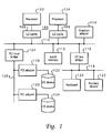
- Data processing system 100 is a symmetric multiprocessor (SMP) system including a plurality of processors 102 and 104 , which preferably comprise one of the PowerPCTM family of processors available from International Business Machines of Armonk, New York. Although only two processors are depicted in the exemplary embodiment, a single or additional processors may be utilized.
- SMP symmetric multiprocessor
- the invention is applicable to other systems besides SMP data processing systems, such as uniprocessor systems, NUMA architecture systems, cluster systems, and the like.
- Each processor 102 and 104 has an associated level two (L2) cache 106 and 108 , respectively, for staging data and instructions to the processors.
- L2 caches 106 and 108 are connected, through L2 caches 106 and 108 , to system bus 110 .
- system bus 110 Also connected to system bus 110 is local memory 112, a memory mapped graphics adapter 114 providing a connection for a display (not shown), and an input/output (I/O) bus bridge 116 coupling system bus 110 to I/O bus 118 .
- I/O input/output
- Input devices such as keyboard 120 and a pointing device 122 , which may be a mouse, trackball, or the like, are connected to I/O bus 118 .
- PCI bus 126 includes a plurality of slots for adapters 128 and 130, connecting nonvolatile storage devices 132 and 134 to PCI bus 126 .
- Nonvolatile storage devices 132 and 134 may be magnetic disk drives, solid state disks, or other conventional storage devices.
- Nonvolatile storage devices 132 and 134 or other devices such as a read only memory (ROM), includes an operating system and related routines which are loaded in response to the system being powered on.
- Such software is loaded into system memory 112 and staged via L2 caches 106 and 108 to processors 102 and 104, as is application software and related data also contained within storage devices 132 and/or 134 .
- Keyboard 120 and pointing device 122 may be employed to control the software applications being executed through a user interface, which may be a graphical user interface.
- data processing system 100 may include many additional components not explicitly shown in Figure 1 , such as serial and parallel ports, connections to networks or attached devices, a controller regulating access to system bus 110 and/or system memory 112 , etc.
- system architecture structures such as NUMA or cluster structures, may be employed. Such modifications and variations are within the scope of the present invention.
- FIG. 2 a diagram of a peripheral component interconnect host bridge in accordance with a preferred embodiment of the present invention is illustrated.
- the problems described earlier can be avoided by delaying reporting of any error until the device driver needs to perform a load from the device for some other reason. At that time, the previous error may be reported.
- the hardware should prevent further load and store operations from reaching the I/O device.
- PCI host bridge 124 Most I/O devices on most I/O buses are selected by address, and may have several address ranges to which they respond.
- typical approaches would involve either duplicating the decoding of I/O devices within the host bridge or shutting off all load and store operations to all devices under a particular host bridge.
- the former solution is not scalable, while the latter will kill many more I/O operations than would be desirable.
- one PCI host bridge may provide connection to four or more I/O devices.
- the problem of preventing loads and stores from completing after an error is solved for PCI-based systems by redesigning PCI host bridge 124 .
- Individual device select (DEVSEL) lines 202a-202n from each I/O device 132 and 134 connected to PCI host bridge 124 are brought into PCI host bridge 124 . This allows each device 132 and 134 to decode its respective address range and report to PCI host bridge 124 if it is selected.
- PCI bus 126 such as a data parity error -- PERR
- the device for which the error occurred is logged in error register 204 via the individual device select lines 202a-202n . From this point until error register 204 within PCI host bridge 124 is cleared, valid data is never passed to the I/O device for which the previous error occurred on a store operation and the I/O device is never permitted to complete a valid read transaction on a load operation.
- FIG. 3A and 3B high level flowcharts for processes of handling of load and store operations on a peripheral component interconnect bus after detection of an error in accordance with a preferred embodiment of the present invention are depicted.
- devices for which an error occurs are logged by the device select associated with the device within an error register in the PCI host bridge. Further load and store operations to I/O device(s) identified in the error register are subsequently prevented from completing.
- Figure 3A depicts a process for a first method of preventing load/store operation from completing to a previously failing device.
- the process begins at step 302 , which illustrates receiving a load or store operation for a device connected to a PCI bus.
- the process then passes to step 304 , which illustrates determining whether the error register in the PCI host bridge is cleared. If not, the process proceeds to step 306 , which depicts delaying completion of a read or write corresponding to the load or store until the device select lines may be read. This may be accomplished using the initiator ready (IRDY) signal line within the PCI bus.
- IRDY initiator ready
- the read or write may be delayed until the device select indicator (also referred to herein as the device identifier or the device number) on the device select lines has been checked against the device number being held in the error register (that is, the device number captured from the previous error).
- the device select indicator also referred to herein as the device identifier or the device number
- step 307 illustrates placing the data with good parity on the bus in preparation for transfer to the I/O device. This allows the store operation to proceed normally if the subject device is not a previously failing device logged in the error register.
- step 308 illustrates a determination, once the device select indicator for the I/O device to which the load or store operation is directed becomes available, of whether the device select indicator is logged in the error register within the PCI host bridge.
- step 310 depicts forcing a data parity error on the operation. For store operations, this may be achieved by changing the parity on the bus to force a data parity error. For load operations, a signal may be transmitted to the PCI host bridge which will be interpreted as though there were bad parity. The PCI host bridge will then naturally signal a parity error (PERR) on the PCI bus to the I/O device, thus signalling the device not to produce any read side effects which would attend a good read operation.
- PRR parity error
- step 312 illustrates terminating the operation. This may be accomplished by activating the initiator ready signal and terminating the operation after one data transfer. Due to the bad data parity, the device should not use any bad data on a store operation or have any read side effects on a load operation. Thus, the operation is essentially a no-op.
- an error may be returned to the processor, which can detect the error and pin the error on the particular device driver performing the operation. The device driver may then clear the error register status in the PCI host bridge for that device to allow further operations to that device. The device driver should then perform appropriate clean-up and rest.
- step 314 which illustrates allowing the operation to continue. This may be accomplished by simply activating the initiator ready signal and permitting the operation to proceed. Load operations, which require the initiator ready signal to proceed in any event, may simply continue after the delay; store operations, if the data with good parity was (optionally) placed on the bus prior to delaying the operation, may also simply continue.
- step 304 if the error register is clear when the load/store operation is received, the process similarly proceeds instead to step 314, which illustrates allowing the operation to proceed normally. Note that the delay of a load/store operation to a "good" I/O device (one not logged in the error register) only occurs until the error register is reset. Therefore the method has no performance impact on normal system operations, only during error recovery. From either of steps 304 or 312 , the process passes to step 314 , which illustrates the process becoming idle until another load or store operation is received.
- Figure 3B depicts a process for a second method of preventing load/store operation from completing to a previously failing device in accordance with the invention.
- the method of Figure 3A involves permitting transfer of the data (or at least a single beat of the data, throwing the rest away) but forcing bad parity on the data.
- This method has a drawback in that the PCI architecture specification does not specify that a device should not use data with bad parity. A good design should not utilize data with bad parity, but doing so would not violate the PCI architecture specification.
- the alternative method depicted in Figure 3B avoids this limitation by setting the byte enables for a data transfer to zero rather than forcing bad parity on the data.
- step 322 which illustrates receiving a load or store operation for a device connected to a PCI bus.
- step 324 which illustrates determining whether the error register in the PCI host bridge is clear. If not, the process proceeds to step 326 , which depicts delaying completion of a read or write corresponding to the load or store operation until the device select lines may be read, by not activating the initiator ready signal as in the first method.
- step 326 the method depicted in Figure 3B varies from the previously described method in that the mechanism employed to prevent completion of load/store operations is actuated before the device number has been checked against the error register.
- step 328 illustrates placing all zero byte enables (BEs) on the bus (that is, all inactive). This will indicate to the I/O device not to pull any data off the bus on a store operation and not to have any side effects from the resulting read on a load operation.
- BEs zero byte enables
- step 330 depicts a determination of whether the device number on the device select lines is contained within the error register on the PCI host bridge, indicating that the device is a previously failing device. If so, the process proceeds to step 332 , which illustrates activating the initiator ready signal and terminating the cycle as described above.
- the bus operation is thus essentially a no-op.
- an error may be returned to the processor to allow the operating system and device driver to clear the PCI host bridge error register and clean up and restart, respectively.
- step 334 depicts terminating and restarting the operation. This may be accomplished by activating the initiator ready signal and allowing the operation to continue (a no-op again), then restarting the operation with the first address and valid byte enables.
- step 336 illustrates allowing the process to continue normally.
- the process also passes to step 336 from step 324 if the error register is clear when the load/store operation is received, so that system performance during normal operations is not affected and operations are only delayed during error recovery. From either of steps 332 or 336 , the process passes to step 338 , which illustrates the process becoming idle until another load/store operation is received.
- the PCI host bridge should also prevent direct memory access (DMA) from the failing device.
- DMA direct memory access
- the PCI host bridge may associate an arbitration level with the device select lines and prevent the failing device from ever receiving a bus grant (GNT) signal.
- the technique of preventing damage to a previously failing I/O device described above may be employed not only for parity errors, but also for any other errors seen on the PCI bus during load or store operations which may be pinned to a particular device, such as a target abort from the target device. Additionally, if an error is received which cannot be pinned to a particular device (such as an address parity error), then the error register may be set to indicate that all I/O devices under that PCI host bridge have had an error, and all subsequent load or store operations to those devices will be flagged as in error.
- the technique of preventing damage to a device may be utilized for errors on the bus on the other side of the PCI host bridge.
- the methods described herein will provide a more workable solution. For example, if a parity error is seen on a store operation to a PCI device, the PCI host bridge may pass that bad parity on to the PCI bus. When the device thereafter responds with a device select, it will also respond with a parity error (PERR) signal. The methods described above will then take effect.
- PERR parity error
- Load/store operations are only delayed if a device has failed and error recovery has not yet completed (if the error register has not yet been reset), and so this does not impact performance during normal system operations.
- Previously failing devices are isolated, and load and store operations to remaining devices are allowed to proceed, even if the target device is under the same PCI host bridge as the previously failing device.
Abstract
Description
- The present invention relates in general to bus error handling in a data processing system or similar, and in particular to handling bus errors during load and store operations.
- Many data processing systems support standard input/output (I/O) systems conforming to the peripheral component interconnect (PCI) Local Bus architecture, an architecture supporting many complex features including I/O expansion through PCI-to-PCI bridges, peer-to-peer (device-to-device) data transfers, multi-function devices, and both integrated and plug-in devices. In setting up I/O operations to I/O devices on a PCI bus, the device driver must perform a series of load and/or store operations to the I/O device. If any of these operations gets a parity error on the I/O bus, it is necessary to get this information back to the device driver so that the device driver can stop before the operation is initiated.
- As an example, a first store operation may be employed to set up an address in the I/O device, followed by a second store operation signalling the I/O device to begin the data transfer. If the first store operation gets an error and the second store operation is then received, the I/O device might start the operation to the incorrect location. The PCI architecture includes no provision for designing adapters to prevent load and/or store operations from continuing after an error. Most contemporary systems allow device driver execution to continue after a store operation rather than wait for a "successful" response to the store operation to determine if it completed correctly. This is preferable since the processor stall required to wait for a response to store operations would vastly degrade system performance.
- One technique allowing the device driver to prevent subsequent load and/or store operations from completing after an error without waiting for the response to every load or store operation is for the device driver to read back all of the setup information before issuing the "go" store operation (the store operation signalling the device driver to begin) and then compare the read back data with the stored data to determine if the two are the same prior to issuing the "go" store operation. However, this requires a lot of processor time for the load operations out to the device, a long path, in many cases, relative to processor instruction times. Another possible solution is to examine bits within the interface or status registers within the I/O device to determine whether an error has occurred after a store operation. This, however, is unsupported by current architectures and also requires a lot of processor time.
- Yet another solution is for an I/O device to generate an external interrupt when there is an error after a store operation, but waiting for an interrupt before continuing takes a lot of time. Other conceivable possibilities will generally be adapter dependent, and thus incapable of working with any I/O device not designed for that solution, or will require a lot of processor time.
- It is desirable, therefore, to provide a method and apparatus for preventing load and/or store operations from completing after an error without waiting for a response to every load or store operation. It is also advantageous for the mechanism to avoid requiring changes to PCI adapter or I/O device hardware, so that the mechanism may be employed with any I/O device, even if not designed specifically for that mechanism.
- Accordingly, the invention provides a method of preventing load or store operations to a previously failing device from completing, comprising:
- responsive to receiving a load or store operation, checking the status of an error register;
- responsive to determining that the error register has not been reset, delaying the load or store operation until a device identifier for a target device for the load or store operation may be checked against the error register; and
- responsive to determining that the device identifier for the target device of the load or store operation is logged within the error register, preventing the load or store operation from completing.
- In the preferred embodiment the step of checking the status of an error register comprises checking the status of an error register within a host bridge, and the step of delaying the load or store operation until a device identifier for the target device for the load or store operation may be checked against the error register comprises delaying a read or write corresponding to the load or store operation until the device identifier becomes available on device select lines connected to a host bridge. Also in the preferred embodiment, the step of delaying the load or store operation until a device identifier for the target device for the load or store operation may be checked against the error register further comprises not activating an initiator ready signal.
- In one preferred embodiment, the step of preventing the load or store operation from completing comprises forcing bad parity on the load or store operation by changing the parity of data on a bus for a store operation, and/or by signalling a parity error to a device on a load operation. This typically results in terminating a data transfer for the load or store operation after transferring a single beat of data.
- In an alternative preferred embodiment, the step of preventing the load or store operation from completing comprises placing all zero byte enables for the load or store operation on a bus. Responsive to determining that the device identifier for the target device of the load or store operation is not logged within the error register, the load or store operation can be terminated and restarted.
- It is preferred that when an error is detected on a bus, a device identifier based on device select line(s) where the error occurred is logged in the error register, and that responsive to determining that the error register has been reset, the load or store operation is allowed to proceed.
- It is also preferred that responsive to determining that the device identifier for the target device of the load or store operation is not logged within the error register, the load or store operation is allowed to proceed, for example by not changing a parity of data on a bus for a store operation; and activating an initiator ready signal.
- The invention further provides a system including a host bridge connecting a bus to a remainder of a data processing system; device select lines connected to the host bridge; and an error register logging a device identifier on the device select lines when an error is detected on the bus, said host bridge including means for preventing load or store operations to a previously failing device from completing, comprising:
- means, responsive to receiving a load or store operation, for checking the status of an error register;
- means, responsive to determining that the error register has not been reset, for delaying the load or store operation until a device identifier for a target device for the load or store operation may be checked against the error register; and
- means, responsive to determining that the device identifier for the target device of the load or store operation is logged within the error register, for preventing the load or store operation from completing.
- It will be appreciated that the system preferably contain features corresponding to the preferred method steps listed above.
- Thus the approach described herein can help to prevent damage from bus errors during load and store operations through identification of a device which previously encountered an error and by use (typically) of forced bad data parity or zero byte enables.
- Thus in the preferred embodiment, device select lines from each I/O device are brought into a PCI host bridge individually so that the device number of a failing device may be logged in an error register when an error is seen on the PCI bus. Until the error register is reset, subsequent load and store operations are delayed until the device number of the subject device may be checked against the error register. If the subject device is a previously failing device, the load/store operation to that device is prevented from completing, either by forcing bad parity or zeroing all byte enables. By forcing bad parity or zero byte enables, the I/O device will respond to the load or store request by activating its device select line, but will not accept store data. Operations to devices which are not logged in the error register are permitted to proceed normally, as are all load store operations when the error register is clear. Normal system operations are thus not impacted, and operations during error recovery are permitted to proceed if no further damage will be caused by such operations.
- A preferred embodiment of the invention will now be described in detail by way of example only with reference to the following drawings:
- Figure 1 depicts a block diagram of a data processing system in which a preferred embodiment of the present invention may be implemented;
- Figure 2 is a diagram of a peripheral component interconnect host bridge in accordance with a preferred embodiment of the present invention; and
- Figures 3A-3B depict high level flowcharts for processes of handling of load and store operations on a peripheral component interconnect bus after detection of an error in accordance with a preferred embodiment of the present invention.
- With reference now to the figures, and in particular with reference to Figure 1, a data processing system in which a preferred embodiment of the present invention may be implemented is depicted.
Data processing system 100 is a symmetric multiprocessor (SMP) system including a plurality ofprocessors - Each
processor cache Processors L2 caches system bus 110. Also connected tosystem bus 110 islocal memory 112, a memory mapped graphics adapter 114 providing a connection for a display (not shown), and an input/output (I/O)bus bridge 116coupling system bus 110 to I/O bus 118. Input devices such askeyboard 120 and apointing device 122, which may be a mouse, trackball, or the like, are connected to I/O bus 118. - Also connected to
system bus 110 is a Peripheral Component Interconnect (PCI)host bridge 124, whichcouples system bus 110 to PCI bus 126. PCI bus 126 includes a plurality of slots foradapters nonvolatile storage devices Nonvolatile storage devices - The operation of
data processing system 100 is known to those in the art. Software contained within storage devices, such asnonvolatile storage devices system memory 112 and staged viaL2 caches processors storage devices 132 and/or 134. Keyboard 120 andpointing device 122 may be employed to control the software applications being executed through a user interface, which may be a graphical user interface. - Those skilled in the art will recognize that
data processing system 100 may include many additional components not explicitly shown in Figure 1, such as serial and parallel ports, connections to networks or attached devices, a controller regulating access tosystem bus 110 and/orsystem memory 112, etc. In addition, other system architecture structures, such as NUMA or cluster structures, may be employed. Such modifications and variations are within the scope of the present invention. - Referring to Figure 2, a diagram of a peripheral component interconnect host bridge in accordance with a preferred embodiment of the present invention is illustrated. In developing a solution to the problem of preventing loads and stores from completing after an error, the problems described earlier can be avoided by delaying reporting of any error until the device driver needs to perform a load from the device for some other reason. At that time, the previous error may be reported. In order for this to be successful, however, there must be a mechanism for preventing further "damage" to the state of an adapter. In order to do this, after the first load or store operation in error to the device, the hardware should prevent further load and store operations from reaching the I/O device.
- Most I/O devices on most I/O buses are selected by address, and may have several address ranges to which they respond. In configuring a host bridge such as
PCI host bridge 124 to prevent load and store operations from reaching an I/O device, typical approaches would involve either duplicating the decoding of I/O devices within the host bridge or shutting off all load and store operations to all devices under a particular host bridge. The former solution is not scalable, while the latter will kill many more I/O operations than would be desirable. For example, one PCI host bridge may provide connection to four or more I/O devices. - In the preferred embodiment, the problem of preventing loads and stores from completing after an error is solved for PCI-based systems by redesigning
PCI host bridge 124. Individual device select (DEVSEL) lines 202a-202n from each I/O device PCI host bridge 124 are brought intoPCI host bridge 124. This allows eachdevice PCI host bridge 124 if it is selected. If an error is detected on a load or store operation to PCI bus 126 (such as a data parity error -- PERR), the device for which the error occurred is logged inerror register 204 via the individual device select lines 202a-202n. From this point until error register 204 withinPCI host bridge 124 is cleared, valid data is never passed to the I/O device for which the previous error occurred on a store operation and the I/O device is never permitted to complete a valid read transaction on a load operation. - Once an error is detected on PCI bus 126, load and store operations to a device are not permitted to complete if the device is one which previously had an error--that is, if the DEVSEL read from device select lines 202a-202n matches the DEVSEL of the I/O adapter which had the error and was logged in
error register 204. Since the DEVSEL signal comes several cycles into the bus operation,PCI host bridge 124 may delay operations to the I/O device until the DEVSEL signal is received. - With reference now to Figures 3A and 3B, high level flowcharts for processes of handling of load and store operations on a peripheral component interconnect bus after detection of an error in accordance with a preferred embodiment of the present invention are depicted. In the preferred embodiment, devices for which an error occurs are logged by the device select associated with the device within an error register in the PCI host bridge. Further load and store operations to I/O device(s) identified in the error register are subsequently prevented from completing.
- Figure 3A depicts a process for a first method of preventing load/store operation from completing to a previously failing device. The process begins at
step 302, which illustrates receiving a load or store operation for a device connected to a PCI bus. The process then passes to step 304, which illustrates determining whether the error register in the PCI host bridge is cleared. If not, the process proceeds to step 306, which depicts delaying completion of a read or write corresponding to the load or store until the device select lines may be read. This may be accomplished using the initiator ready (IRDY) signal line within the PCI bus. By not activating the initiator ready line, the read or write may be delayed until the device select indicator (also referred to herein as the device identifier or the device number) on the device select lines has been checked against the device number being held in the error register (that is, the device number captured from the previous error). - For store operations, the process may optionally proceed to step 307, which illustrates placing the data with good parity on the bus in preparation for transfer to the I/O device. This allows the store operation to proceed normally if the subject device is not a previously failing device logged in the error register. From
step 307, if implemented, and otherwise fromstep 306, the process then passes to step 308, which illustrates a determination, once the device select indicator for the I/O device to which the load or store operation is directed becomes available, of whether the device select indicator is logged in the error register within the PCI host bridge. - If the device select indicator is logged in the error register, identifying a previously failing device, the process proceeds to step 310, which depicts forcing a data parity error on the operation. For store operations, this may be achieved by changing the parity on the bus to force a data parity error. For load operations, a signal may be transmitted to the PCI host bridge which will be interpreted as though there were bad parity. The PCI host bridge will then naturally signal a parity error (PERR) on the PCI bus to the I/O device, thus signalling the device not to produce any read side effects which would attend a good read operation.
- The process then passes to step 312, which illustrates terminating the operation. This may be accomplished by activating the initiator ready signal and terminating the operation after one data transfer. Due to the bad data parity, the device should not use any bad data on a store operation or have any read side effects on a load operation. Thus, the operation is essentially a no-op. On a load operation, an error may be returned to the processor, which can detect the error and pin the error on the particular device driver performing the operation. The device driver may then clear the error register status in the PCI host bridge for that device to allow further operations to that device. The device driver should then perform appropriate clean-up and rest.
- Referring again to step 308, if the device select indicator does not match any device number within the PCI host bridge error register, indicating that the device is not a previously failing device, then the process proceeds instead to step 314, which illustrates allowing the operation to continue. This may be accomplished by simply activating the initiator ready signal and permitting the operation to proceed. Load operations, which require the initiator ready signal to proceed in any event, may simply continue after the delay; store operations, if the data with good parity was (optionally) placed on the bus prior to delaying the operation, may also simply continue.
- Referring back to step 304, if the error register is clear when the load/store operation is received, the process similarly proceeds instead to step 314, which illustrates allowing the operation to proceed normally. Note that the delay of a load/store operation to a "good" I/O device (one not logged in the error register) only occurs until the error register is reset. Therefore the method has no performance impact on normal system operations, only during error recovery. From either of
steps 304 or 312, the process passes to step 314, which illustrates the process becoming idle until another load or store operation is received. - Figure 3B depicts a process for a second method of preventing load/store operation from completing to a previously failing device in accordance with the invention. The method of Figure 3A involves permitting transfer of the data (or at least a single beat of the data, throwing the rest away) but forcing bad parity on the data. This method has a drawback in that the PCI architecture specification does not specify that a device should not use data with bad parity. A good design should not utilize data with bad parity, but doing so would not violate the PCI architecture specification. The alternative method depicted in Figure 3B avoids this limitation by setting the byte enables for a data transfer to zero rather than forcing bad parity on the data. This has the advantage of being explicitly addressed in the PCI architecture specification, which states that the target of an access where no byte enables are asserted must complete the current data phase without any permanent change. The PCI architecture specification further indicates that: on a read transaction, this means that data or status are not changed; on a write transaction, the data is not stored.
- The process depicted in Figure 3B begins at
step 322, which illustrates receiving a load or store operation for a device connected to a PCI bus. The process then passes to step 324, which illustrates determining whether the error register in the PCI host bridge is clear. If not, the process proceeds to step 326, which depicts delaying completion of a read or write corresponding to the load or store operation until the device select lines may be read, by not activating the initiator ready signal as in the first method. - From
step 326, the method depicted in Figure 3B varies from the previously described method in that the mechanism employed to prevent completion of load/store operations is actuated before the device number has been checked against the error register. Thus, the process passes to step 328, which illustrates placing all zero byte enables (BEs) on the bus (that is, all inactive). This will indicate to the I/O device not to pull any data off the bus on a store operation and not to have any side effects from the resulting read on a load operation. - The process next passes to step 330, which depicts a determination of whether the device number on the device select lines is contained within the error register on the PCI host bridge, indicating that the device is a previously failing device. If so, the process proceeds to step 332, which illustrates activating the initiator ready signal and terminating the cycle as described above. The bus operation is thus essentially a no-op. As previously described, an error may be returned to the processor to allow the operating system and device driver to clear the PCI host bridge error register and clean up and restart, respectively.
- If the device number does not match the device identifier logged in the error register, the process proceeds instead to step 334, which depicts terminating and restarting the operation. This may be accomplished by activating the initiator ready signal and allowing the operation to continue (a no-op again), then restarting the operation with the first address and valid byte enables. The process next passes to step 336, which illustrates allowing the process to continue normally. As with the previous method, the process also passes to step 336 from
step 324 if the error register is clear when the load/store operation is received, so that system performance during normal operations is not affected and operations are only delayed during error recovery. From either ofsteps - The two alternative methods depicted in Figures 3A and 3B both have advantages and limitations. Forcing bad parity on the data allows operations to devices not logged in the error register to proceed without unnecessary delay, but does not ensure that bad data will not be utilized. Zeroing the byte enables prevents bad data from being employed, but requires operations to "good" devices (those not logged in the error register) to be terminated and restarted. The best method may thus depend on the circumstances of each particular implementation.
- In addition to preventing load and store operations to previously failing devices from completing, the PCI host bridge should also prevent direct memory access (DMA) from the failing device. To do that, the PCI host bridge may associate an arbitration level with the device select lines and prevent the failing device from ever receiving a bus grant (GNT) signal.
- The technique of preventing damage to a previously failing I/O device described above may be employed not only for parity errors, but also for any other errors seen on the PCI bus during load or store operations which may be pinned to a particular device, such as a target abort from the target device. Additionally, if an error is received which cannot be pinned to a particular device (such as an address parity error), then the error register may be set to indicate that all I/O devices under that PCI host bridge have had an error, and all subsequent load or store operations to those devices will be flagged as in error.
- In addition to errors seen on the PCI bus, the technique of preventing damage to a device may be utilized for errors on the bus on the other side of the PCI host bridge. As long as the error may be pinned to a particular PCI device, the methods described herein will provide a more workable solution. For example, if a parity error is seen on a store operation to a PCI device, the PCI host bridge may pass that bad parity on to the PCI bus. When the device thereafter responds with a device select, it will also respond with a parity error (PERR) signal. The methods described above will then take effect.
- The approach described herein prevents completion of load and store operations to a previously failing device without requiring any changes to PCI adapter hardware and without requiring a substantial amount of processor time. Load/store operations are only delayed if a device has failed and error recovery has not yet completed (if the error register has not yet been reset), and so this does not impact performance during normal system operations. Previously failing devices are isolated, and load and store operations to remaining devices are allowed to proceed, even if the target device is under the same PCI host bridge as the previously failing device.
Claims (16)
- A method of preventing load or store operations to a previously failing device from completing, comprising:responsive to receiving a load or store operation, checking (304) the status of an error register (204);responsive to determining that the error register has not been reset, delaying (306) the load or store operation until a device identifier for a target device for the load or store operation may be checked against the error register; andresponsive to determining that the device identifier for the target device of the load or store operation is logged within the error register, preventing the load or store operation from completing.
- The method of claim 1, wherein the step of checking the status of an error register comprises checking the status of an error register within a host bridge (124).
- The method of claim 1 or 2, wherein the step of delaying the load or store operation until a device identifier for the target device for the load or store operation may be checked against the error register comprises delaying a read or write corresponding to the load or store operation until the device identifier becomes available on device select lines (202n) connected to a host bridge.
- The method of any preceding claim, wherein the step of delaying the load or store operation until a device identifier for the target device for the load or store operation may be checked against the error register further comprises not activating an initiator ready signal.
- The method of any preceding claim, wherein the step of preventing the load or store operation from completing comprises forcing (310) bad parity on the load or store operation.
- The method of claim 5, wherein the step of forcing bad parity on the load or store operation comprises changing the parity of data on a bus for a store operation.
- The method of claim 5 or 6, wherein the step of forcing bad parity on the load or store operation further comprises signalling a parity error to a device on a load operation.
- The method of any of claims 5 to 7, further comprising terminating a data transfer for the load or store operation after transferring a single beat of data.
- The method of any of claims 1 to 4, wherein the step of preventing the load or store operation from completing comprises placing (328) all zero byte enables for the load or store operation on a bus.
- The method of claim 9, further comprising, responsive to determining that the device identifier for the target device of the load or store operation is not logged within the error register, terminating and restarting (334) the load or store operation.
- The method of any preceding claim, further comprising, upon detecting an error on a bus, logging in the error register a device identifier based on device select line(s) where the error occurred.
- The method of claim 1, further comprising, responsive to determining that the device identifier for the target device of the load or store operation is not logged within the error register, allowing (314) the load or store operation to proceed.
- The method of claim 12, wherein the step of allowing the load or store operation to proceed further comprises not changing a parity of data on a bus for a store operation; and activating an initiator ready signal.
- The method of any preceding claim, further comprising, responsive to determining that the error register has been reset, allowing (314) the load or store operation to proceed.
- A system including a host bridge (124) connecting a bus (126) to a remainder of a data processing system; device select lines (202n) connected to the host bridge; and an error register (204) logging a device identifier on the device select lines when an error is detected on the bus, said host bridge including means for preventing load or store operations to a previously failing device from completing, comprising:means, responsive to receiving a load or store operation, for checking the status of an error register;means, responsive to determining that the error register has not been reset, for delaying the load or store operation until a device identifier for a target device for the load or store operation may be checked against the error register; andmeans, responsive to determining that the device identifier for the target device of the load or store operation is logged within the error register, for preventing the load or store operation from completing.
- The mechanism of claim 15, wherein the error register is contained within the host bridge.
Applications Claiming Priority (2)
| Application Number | Priority Date | Filing Date | Title |
|---|---|---|---|
| US72418 | 1987-07-13 | ||
| US09/072,418 US6223299B1 (en) | 1998-05-04 | 1998-05-04 | Enhanced error handling for I/O load/store operations to a PCI device via bad parity or zero byte enables |
Publications (3)
| Publication Number | Publication Date |
|---|---|
| EP0955585A2 true EP0955585A2 (en) | 1999-11-10 |
| EP0955585A3 EP0955585A3 (en) | 2003-03-19 |
| EP0955585B1 EP0955585B1 (en) | 2004-02-25 |
Family
ID=22107431
Family Applications (1)
| Application Number | Title | Priority Date | Filing Date |
|---|---|---|---|
| EP99302989A Expired - Lifetime EP0955585B1 (en) | 1998-05-04 | 1999-04-19 | Method and system for handling bus errors in a data processing system |
Country Status (7)
| Country | Link |
|---|---|
| US (1) | US6223299B1 (en) |
| EP (1) | EP0955585B1 (en) |
| JP (1) | JP3437939B2 (en) |
| KR (1) | KR100337215B1 (en) |
| CN (1) | CN1139036C (en) |
| DE (1) | DE69914966D1 (en) |
| TW (1) | TW424179B (en) |
Cited By (19)
| Publication number | Priority date | Publication date | Assignee | Title |
|---|---|---|---|---|
| WO2011160712A1 (en) * | 2010-06-23 | 2011-12-29 | International Business Machines Corporation | Managing processing associated with hardware events |
| US8458387B2 (en) | 2010-06-23 | 2013-06-04 | International Business Machines Corporation | Converting a message signaled interruption into an I/O adapter event notification to a guest operating system |
| US8478922B2 (en) | 2010-06-23 | 2013-07-02 | International Business Machines Corporation | Controlling a rate at which adapter interruption requests are processed |
| US8504754B2 (en) | 2010-06-23 | 2013-08-06 | International Business Machines Corporation | Identification of types of sources of adapter interruptions |
| US8505032B2 (en) | 2010-06-23 | 2013-08-06 | International Business Machines Corporation | Operating system notification of actions to be taken responsive to adapter events |
| US8549182B2 (en) | 2010-06-23 | 2013-10-01 | International Business Machines Corporation | Store/store block instructions for communicating with adapters |
| US8566480B2 (en) | 2010-06-23 | 2013-10-22 | International Business Machines Corporation | Load instruction for communicating with adapters |
| US8572635B2 (en) | 2010-06-23 | 2013-10-29 | International Business Machines Corporation | Converting a message signaled interruption into an I/O adapter event notification |
| US8615645B2 (en) | 2010-06-23 | 2013-12-24 | International Business Machines Corporation | Controlling the selectively setting of operational parameters for an adapter |
| US8621112B2 (en) | 2010-06-23 | 2013-12-31 | International Business Machines Corporation | Discovery by operating system of information relating to adapter functions accessible to the operating system |
| US8626970B2 (en) | 2010-06-23 | 2014-01-07 | International Business Machines Corporation | Controlling access by a configuration to an adapter function |
| US8631222B2 (en) | 2010-06-23 | 2014-01-14 | International Business Machines Corporation | Translation of input/output addresses to memory addresses |
| US8639858B2 (en) | 2010-06-23 | 2014-01-28 | International Business Machines Corporation | Resizing address spaces concurrent to accessing the address spaces |
| US8650335B2 (en) | 2010-06-23 | 2014-02-11 | International Business Machines Corporation | Measurement facility for adapter functions |
| US8650337B2 (en) | 2010-06-23 | 2014-02-11 | International Business Machines Corporation | Runtime determination of translation formats for adapter functions |
| WO2015013460A1 (en) * | 2013-07-23 | 2015-01-29 | Qualcomm Incorporated | Robust hardware/software error recovery system |
| US9195623B2 (en) | 2010-06-23 | 2015-11-24 | International Business Machines Corporation | Multiple address spaces per adapter with address translation |
| US9213661B2 (en) | 2010-06-23 | 2015-12-15 | International Business Machines Corporation | Enable/disable adapters of a computing environment |
| US9342352B2 (en) | 2010-06-23 | 2016-05-17 | International Business Machines Corporation | Guest access to address spaces of adapter |
Families Citing this family (20)
| Publication number | Priority date | Publication date | Assignee | Title |
|---|---|---|---|---|
| FI19991735A (en) * | 1999-08-16 | 2001-02-17 | Nokia Networks Oy | A method and apparatus for improving the reliability of a computer system |
| US6643727B1 (en) * | 2000-06-08 | 2003-11-04 | International Business Machines Corporation | Isolation of I/O bus errors to a single partition in an LPAR environment |
| US6665753B1 (en) * | 2000-08-10 | 2003-12-16 | International Business Machines Corporation | Performance enhancement implementation through buffer management/bridge settings |
| US6934888B2 (en) * | 2002-03-07 | 2005-08-23 | International Business Machines Corporation | Method and apparatus for enhancing input/output error analysis in hardware sub-systems |
| US6976191B2 (en) * | 2002-03-07 | 2005-12-13 | International Business Machines Corporation | Method and apparatus for analyzing hardware errors in a logical partitioned data processing system |
| US20040008192A1 (en) * | 2002-07-10 | 2004-01-15 | Waterman John Karl | Parity checking system and method for a display system |
| US7650530B2 (en) * | 2002-09-30 | 2010-01-19 | International Business Machines Corporation | Initializing a processing system to ensure fail-safe boot when faulty PCI adapters are present |
| JP4123942B2 (en) * | 2003-01-14 | 2008-07-23 | 株式会社日立製作所 | Information processing device |
| JP4153802B2 (en) * | 2003-02-07 | 2008-09-24 | 株式会社ルネサステクノロジ | Storage device |
| US7103808B2 (en) * | 2003-04-10 | 2006-09-05 | International Business Machines Corporation | Apparatus for reporting and isolating errors below a host bridge |
| CN1302358C (en) * | 2003-05-21 | 2007-02-28 | 华为技术有限公司 | Resettnig method of bridging chip and apparatus thereof |
| US7877647B2 (en) * | 2003-05-23 | 2011-01-25 | Hewlett-Packard Development Company, L.P. | Correcting a target address in parallel with determining whether the target address was received in error |
| US7275199B2 (en) * | 2004-08-05 | 2007-09-25 | International Business Machines Corporation | Method and apparatus for a modified parity check |
| CN100372094C (en) * | 2004-10-29 | 2008-02-27 | 力晶半导体股份有限公司 | Wafer testing device and method with automatic reversion function |
| US20060271718A1 (en) * | 2005-05-27 | 2006-11-30 | Diplacido Bruno Jr | Method of preventing error propagation in a PCI / PCI-X / PCI express link |
| US7412629B2 (en) * | 2005-06-09 | 2008-08-12 | International Business Machines Corporation | Method to override daughterboard slots marked with power fault |
| US20080148104A1 (en) * | 2006-09-01 | 2008-06-19 | Brinkman Michael G | Detecting an Agent Generating a Parity Error on a PCI-Compatible Bus |
| JP4656080B2 (en) * | 2007-04-16 | 2011-03-23 | 株式会社日立製作所 | System parts for information processing equipment |
| CN101625656B (en) * | 2009-07-28 | 2012-09-19 | 杭州华三通信技术有限公司 | Method and device for processing abnormity of PCI system |
| JP5201176B2 (en) * | 2010-07-09 | 2013-06-05 | 株式会社日立製作所 | Information processing device |
Citations (2)
| Publication number | Priority date | Publication date | Assignee | Title |
|---|---|---|---|---|
| EP0628910A1 (en) * | 1993-05-28 | 1994-12-14 | International Business Machines Corporation | Error capture logic for peripheral bus in multiple bus computer system |
| US5687183A (en) * | 1991-12-18 | 1997-11-11 | Sun Microsystems, Inc. | Memory access system with overwrite prevention for overlapping write operations |
Family Cites Families (10)
| Publication number | Priority date | Publication date | Assignee | Title |
|---|---|---|---|---|
| US5404483A (en) * | 1990-06-29 | 1995-04-04 | Digital Equipment Corporation | Processor and method for delaying the processing of cache coherency transactions during outstanding cache fills |
| US5313627A (en) * | 1992-01-02 | 1994-05-17 | International Business Machines Corp. | Parity error detection and recovery |
| US5522050A (en) * | 1993-05-28 | 1996-05-28 | International Business Machines Corporation | Bus-to-bus bridge for a multiple bus information handling system that optimizes data transfers between a system bus and a peripheral bus |
| US5790831A (en) * | 1994-11-01 | 1998-08-04 | Opti Inc. | VL-bus/PCI-bus bridge |
| CA2160500C (en) * | 1994-11-30 | 1999-11-09 | Amy Kulik | Pci/isa bridge having an arrangement for responding to pci bridge address parity errors for internal pci slaves in the pci/isa bridge |
| US5859988A (en) * | 1995-09-29 | 1999-01-12 | Intel Corporation | Triple-port bus bridge |
| KR100244836B1 (en) * | 1995-11-02 | 2000-02-15 | 포만 제프리 엘 | Error recovery by isolation of peripheral components in a data processing system |
| US5857080A (en) * | 1996-09-10 | 1999-01-05 | Lsi Logic Corporation | Apparatus and method for address translation in bus bridge devices |
| US5857085A (en) * | 1996-11-13 | 1999-01-05 | Cypress Semiconductor Corporation | Interface device for XT/AT system devices on high speed local bus |
| US5872910A (en) * | 1996-12-27 | 1999-02-16 | Unisys Corporation | Parity-error injection system for an instruction processor |
-
1998
- 1998-05-04 US US09/072,418 patent/US6223299B1/en not_active Expired - Lifetime
-
1999
- 1999-04-02 CN CNB991047877A patent/CN1139036C/en not_active Expired - Lifetime
- 1999-04-15 KR KR1019990013381A patent/KR100337215B1/en not_active IP Right Cessation
- 1999-04-19 EP EP99302989A patent/EP0955585B1/en not_active Expired - Lifetime
- 1999-04-19 JP JP11065099A patent/JP3437939B2/en not_active Expired - Fee Related
- 1999-04-19 DE DE69914966T patent/DE69914966D1/en not_active Expired - Lifetime
- 1999-04-23 TW TW088106471A patent/TW424179B/en not_active IP Right Cessation
Patent Citations (2)
| Publication number | Priority date | Publication date | Assignee | Title |
|---|---|---|---|---|
| US5687183A (en) * | 1991-12-18 | 1997-11-11 | Sun Microsystems, Inc. | Memory access system with overwrite prevention for overlapping write operations |
| EP0628910A1 (en) * | 1993-05-28 | 1994-12-14 | International Business Machines Corporation | Error capture logic for peripheral bus in multiple bus computer system |
Cited By (27)
| Publication number | Priority date | Publication date | Assignee | Title |
|---|---|---|---|---|
| US8621112B2 (en) | 2010-06-23 | 2013-12-31 | International Business Machines Corporation | Discovery by operating system of information relating to adapter functions accessible to the operating system |
| US9626298B2 (en) | 2010-06-23 | 2017-04-18 | International Business Machines Corporation | Translation of input/output addresses to memory addresses |
| WO2011160712A1 (en) * | 2010-06-23 | 2011-12-29 | International Business Machines Corporation | Managing processing associated with hardware events |
| US8478922B2 (en) | 2010-06-23 | 2013-07-02 | International Business Machines Corporation | Controlling a rate at which adapter interruption requests are processed |
| US8504754B2 (en) | 2010-06-23 | 2013-08-06 | International Business Machines Corporation | Identification of types of sources of adapter interruptions |
| US8505032B2 (en) | 2010-06-23 | 2013-08-06 | International Business Machines Corporation | Operating system notification of actions to be taken responsive to adapter events |
| US8510599B2 (en) | 2010-06-23 | 2013-08-13 | International Business Machines Corporation | Managing processing associated with hardware events |
| US8549182B2 (en) | 2010-06-23 | 2013-10-01 | International Business Machines Corporation | Store/store block instructions for communicating with adapters |
| US8566480B2 (en) | 2010-06-23 | 2013-10-22 | International Business Machines Corporation | Load instruction for communicating with adapters |
| US8572635B2 (en) | 2010-06-23 | 2013-10-29 | International Business Machines Corporation | Converting a message signaled interruption into an I/O adapter event notification |
| US8601497B2 (en) | 2010-06-23 | 2013-12-03 | International Business Machines Corporation | Converting a message signaled interruption into an I/O adapter event notification |
| US8615645B2 (en) | 2010-06-23 | 2013-12-24 | International Business Machines Corporation | Controlling the selectively setting of operational parameters for an adapter |
| US8468284B2 (en) | 2010-06-23 | 2013-06-18 | International Business Machines Corporation | Converting a message signaled interruption into an I/O adapter event notification to a guest operating system |
| US8458387B2 (en) | 2010-06-23 | 2013-06-04 | International Business Machines Corporation | Converting a message signaled interruption into an I/O adapter event notification to a guest operating system |
| US9195623B2 (en) | 2010-06-23 | 2015-11-24 | International Business Machines Corporation | Multiple address spaces per adapter with address translation |
| US8635430B2 (en) | 2010-06-23 | 2014-01-21 | International Business Machines Corporation | Translation of input/output addresses to memory addresses |
| US8639858B2 (en) | 2010-06-23 | 2014-01-28 | International Business Machines Corporation | Resizing address spaces concurrent to accessing the address spaces |
| US8650335B2 (en) | 2010-06-23 | 2014-02-11 | International Business Machines Corporation | Measurement facility for adapter functions |
| US8650337B2 (en) | 2010-06-23 | 2014-02-11 | International Business Machines Corporation | Runtime determination of translation formats for adapter functions |
| US8626970B2 (en) | 2010-06-23 | 2014-01-07 | International Business Machines Corporation | Controlling access by a configuration to an adapter function |
| US9134911B2 (en) | 2010-06-23 | 2015-09-15 | International Business Machines Corporation | Store peripheral component interconnect (PCI) function controls instruction |
| US8631222B2 (en) | 2010-06-23 | 2014-01-14 | International Business Machines Corporation | Translation of input/output addresses to memory addresses |
| US9213661B2 (en) | 2010-06-23 | 2015-12-15 | International Business Machines Corporation | Enable/disable adapters of a computing environment |
| US9342352B2 (en) | 2010-06-23 | 2016-05-17 | International Business Machines Corporation | Guest access to address spaces of adapter |
| US9383931B2 (en) | 2010-06-23 | 2016-07-05 | International Business Machines Corporation | Controlling the selectively setting of operational parameters for an adapter |
| US9442793B2 (en) | 2013-07-23 | 2016-09-13 | Qualcomm Incorporated | Robust hardware/software error recovery system |
| WO2015013460A1 (en) * | 2013-07-23 | 2015-01-29 | Qualcomm Incorporated | Robust hardware/software error recovery system |
Also Published As
| Publication number | Publication date |
|---|---|
| JP3437939B2 (en) | 2003-08-18 |
| CN1234562A (en) | 1999-11-10 |
| CN1139036C (en) | 2004-02-18 |
| EP0955585B1 (en) | 2004-02-25 |
| US6223299B1 (en) | 2001-04-24 |
| KR19990087931A (en) | 1999-12-27 |
| KR100337215B1 (en) | 2002-05-17 |
| TW424179B (en) | 2001-03-01 |
| EP0955585A3 (en) | 2003-03-19 |
| JPH11353244A (en) | 1999-12-24 |
| DE69914966D1 (en) | 2004-04-01 |
Similar Documents
| Publication | Publication Date | Title |
|---|---|---|
| EP0955585B1 (en) | Method and system for handling bus errors in a data processing system | |
| US6304984B1 (en) | Method and system for injecting errors to a device within a computer system | |
| US6018810A (en) | Fault-tolerant interconnection means in a computer system | |
| US6182248B1 (en) | Method and tool for computer bus fault isolation and recovery design verification | |
| US6523140B1 (en) | Computer system error recovery and fault isolation | |
| US5499346A (en) | Bus-to-bus bridge for a multiple bus information handling system that optimizes data transfers between a system bus and a peripheral bus | |
| US5596716A (en) | Method and apparatus for indicating the severity of a fault within a computer system | |
| US5666559A (en) | Fail-safe communication abort mechanism for parallel ports with selectable NMI or parallel port interrupt | |
| US6502156B1 (en) | Controlling I/O devices independently of a host processor | |
| RU2137182C1 (en) | Execution of data processing instruction | |
| JP2002518745A (en) | Bus controller with cycle end monitor | |
| JP2002518735A (en) | Processor bridge with heterogeneous data registers | |
| US5680537A (en) | Method and apparatus for isolating an error within a computer system that transfers data via an interface device | |
| US7631226B2 (en) | Computer system, bus controller, and bus fault handling method used in the same computer system and bus controller | |
| WO1998014880A1 (en) | Method and apparatus for changing data transfer widths in a computer system | |
| US7685473B2 (en) | Computer system, method of detecting a stall in a computer system, and signal-bearing medium embodying a program causing a computer system to perform a method of detecting a stall in a computer system | |
| US6584586B1 (en) | Apparatus and method for capturing and transferring internal system activity | |
| US6732298B1 (en) | Nonmaskable interrupt workaround for a single exception interrupt handler processor | |
| US7054987B1 (en) | Apparatus, system, and method for avoiding data writes that stall transactions in a bus interface | |
| US5867728A (en) | Preventing corruption in a multiple processor computer system during a peripheral device configuration cycle | |
| US5293384A (en) | Microprocessor bus interface protocol analyzer | |
| US6189117B1 (en) | Error handling between a processor and a system managed by the processor | |
| US6643796B1 (en) | Method and apparatus for providing cooperative fault recovery between a processor and a service processor | |
| EP0764907A1 (en) | Method and system for error recovery in a data processing system | |
| EP0596410B1 (en) | Detection of command synchronisation error |
Legal Events
| Date | Code | Title | Description |
|---|---|---|---|
| PUAI | Public reference made under article 153(3) epc to a published international application that has entered the european phase |
Free format text: ORIGINAL CODE: 0009012 |
|
| AK | Designated contracting states |
Kind code of ref document: A2 Designated state(s): AT BE CH CY DE DK ES FI FR GB GR IE IT LI LU MC NL PT SE |
|
| AX | Request for extension of the european patent |
Free format text: AL;LT;LV;MK;RO;SI |
|
| PUAL | Search report despatched |
Free format text: ORIGINAL CODE: 0009013 |
|
| AK | Designated contracting states |
Kind code of ref document: A3 Designated state(s): AT BE CH CY DE DK ES FI FR GB GR IE IT LI LU MC NL PT SE Designated state(s): AT BE CH CY DE DK ES FI FR GB GR IE IT LI LU MC NL PT SE |
|
| AX | Request for extension of the european patent |
Extension state: AL LT LV MK RO SI |
|
| 17P | Request for examination filed |
Effective date: 20030414 |
|
| GRAP | Despatch of communication of intention to grant a patent |
Free format text: ORIGINAL CODE: EPIDOSNIGR1 |
|
| GRAS | Grant fee paid |
Free format text: ORIGINAL CODE: EPIDOSNIGR3 |
|
| AKX | Designation fees paid |
Designated state(s): DE FR GB |
|
| GRAA | (expected) grant |
Free format text: ORIGINAL CODE: 0009210 |
|
| AK | Designated contracting states |
Kind code of ref document: B1 Designated state(s): DE FR GB |
|
| PG25 | Lapsed in a contracting state [announced via postgrant information from national office to epo] |
Ref country code: FR Free format text: LAPSE BECAUSE OF FAILURE TO SUBMIT A TRANSLATION OF THE DESCRIPTION OR TO PAY THE FEE WITHIN THE PRESCRIBED TIME-LIMIT Effective date: 20040225 |
|
| REG | Reference to a national code |
Ref country code: GB Ref legal event code: FG4D |
|
| REG | Reference to a national code |
Ref country code: IE Ref legal event code: FG4D |
|
| REF | Corresponds to: |
Ref document number: 69914966 Country of ref document: DE Date of ref document: 20040401 Kind code of ref document: P |
|
| PG25 | Lapsed in a contracting state [announced via postgrant information from national office to epo] |
Ref country code: DE Free format text: LAPSE BECAUSE OF FAILURE TO SUBMIT A TRANSLATION OF THE DESCRIPTION OR TO PAY THE FEE WITHIN THE PRESCRIBED TIME-LIMIT Effective date: 20040526 |
|
| PLBE | No opposition filed within time limit |
Free format text: ORIGINAL CODE: 0009261 |
|
| STAA | Information on the status of an ep patent application or granted ep patent |
Free format text: STATUS: NO OPPOSITION FILED WITHIN TIME LIMIT |
|
| REG | Reference to a national code |
Ref country code: IE Ref legal event code: MM4A |
|
| EN | Fr: translation not filed | ||
| 26N | No opposition filed |
Effective date: 20041126 |
|
| REG | Reference to a national code |
Ref country code: GB Ref legal event code: 746 Effective date: 20080329 |
|
| PGFP | Annual fee paid to national office [announced via postgrant information from national office to epo] |
Ref country code: GB Payment date: 20180405 Year of fee payment: 20 |
|
| REG | Reference to a national code |
Ref country code: GB Ref legal event code: PE20 Expiry date: 20190418 |
|
| PG25 | Lapsed in a contracting state [announced via postgrant information from national office to epo] |
Ref country code: GB Free format text: LAPSE BECAUSE OF EXPIRATION OF PROTECTION Effective date: 20190418 |