EP0962999A2 - Resonator structures - Google Patents
Resonator structures Download PDFInfo
- Publication number
- EP0962999A2 EP0962999A2 EP99304277A EP99304277A EP0962999A2 EP 0962999 A2 EP0962999 A2 EP 0962999A2 EP 99304277 A EP99304277 A EP 99304277A EP 99304277 A EP99304277 A EP 99304277A EP 0962999 A2 EP0962999 A2 EP 0962999A2
- Authority
- EP
- European Patent Office
- Prior art keywords
- resonator
- substrate
- structures
- switch
- resonators
- Prior art date
- Legal status (The legal status is an assumption and is not a legal conclusion. Google has not performed a legal analysis and makes no representation as to the accuracy of the status listed.)
- Ceased
Links
- 239000000758 substrate Substances 0.000 claims abstract description 74
- 238000010295 mobile communication Methods 0.000 claims abstract description 15
- 230000008021 deposition Effects 0.000 claims description 14
- 238000010897 surface acoustic wave method Methods 0.000 claims description 13
- 238000000059 patterning Methods 0.000 claims description 10
- 238000000034 method Methods 0.000 abstract description 14
- XUIMIQQOPSSXEZ-UHFFFAOYSA-N Silicon Chemical compound [Si] XUIMIQQOPSSXEZ-UHFFFAOYSA-N 0.000 abstract description 8
- 229910052710 silicon Inorganic materials 0.000 abstract description 8
- 239000010703 silicon Substances 0.000 abstract description 8
- 238000004519 manufacturing process Methods 0.000 abstract description 7
- JBRZTFJDHDCESZ-UHFFFAOYSA-N AsGa Chemical compound [As]#[Ga] JBRZTFJDHDCESZ-UHFFFAOYSA-N 0.000 abstract description 6
- 230000008569 process Effects 0.000 abstract description 5
- 230000010354 integration Effects 0.000 abstract description 4
- 238000004891 communication Methods 0.000 abstract description 2
- 239000000463 material Substances 0.000 description 23
- 238000000151 deposition Methods 0.000 description 10
- 230000005540 biological transmission Effects 0.000 description 9
- 239000012528 membrane Substances 0.000 description 9
- 230000008901 benefit Effects 0.000 description 8
- 229920000642 polymer Polymers 0.000 description 8
- 239000010409 thin film Substances 0.000 description 7
- VYPSYNLAJGMNEJ-UHFFFAOYSA-N Silicium dioxide Chemical compound O=[Si]=O VYPSYNLAJGMNEJ-UHFFFAOYSA-N 0.000 description 4
- XLOMVQKBTHCTTD-UHFFFAOYSA-N Zinc monoxide Chemical compound [Zn]=O XLOMVQKBTHCTTD-UHFFFAOYSA-N 0.000 description 4
- 239000000919 ceramic Substances 0.000 description 4
- 230000008859 change Effects 0.000 description 4
- 239000010949 copper Substances 0.000 description 4
- 230000009977 dual effect Effects 0.000 description 4
- 238000005530 etching Methods 0.000 description 4
- 238000001914 filtration Methods 0.000 description 4
- 239000010931 gold Substances 0.000 description 4
- 229910052751 metal Inorganic materials 0.000 description 4
- 239000002184 metal Substances 0.000 description 4
- PXHVJJICTQNCMI-UHFFFAOYSA-N Nickel Chemical compound [Ni] PXHVJJICTQNCMI-UHFFFAOYSA-N 0.000 description 3
- 239000004642 Polyimide Substances 0.000 description 3
- 238000011161 development Methods 0.000 description 3
- 239000011521 glass Substances 0.000 description 3
- 238000002955 isolation Methods 0.000 description 3
- 229920001721 polyimide Polymers 0.000 description 3
- CFAKWWQIUFSQFU-UHFFFAOYSA-N 2-hydroxy-3-methylcyclopent-2-en-1-one Chemical compound CC1=C(O)C(=O)CC1 CFAKWWQIUFSQFU-UHFFFAOYSA-N 0.000 description 2
- RYGMFSIKBFXOCR-UHFFFAOYSA-N Copper Chemical compound [Cu] RYGMFSIKBFXOCR-UHFFFAOYSA-N 0.000 description 2
- ZOKXTWBITQBERF-UHFFFAOYSA-N Molybdenum Chemical compound [Mo] ZOKXTWBITQBERF-UHFFFAOYSA-N 0.000 description 2
- RTAQQCXQSZGOHL-UHFFFAOYSA-N Titanium Chemical compound [Ti] RTAQQCXQSZGOHL-UHFFFAOYSA-N 0.000 description 2
- 229910052782 aluminium Inorganic materials 0.000 description 2
- XAGFODPZIPBFFR-UHFFFAOYSA-N aluminium Chemical compound [Al] XAGFODPZIPBFFR-UHFFFAOYSA-N 0.000 description 2
- 239000003990 capacitor Substances 0.000 description 2
- 239000002131 composite material Substances 0.000 description 2
- 229910052802 copper Inorganic materials 0.000 description 2
- PCHJSUWPFVWCPO-UHFFFAOYSA-N gold Chemical compound [Au] PCHJSUWPFVWCPO-UHFFFAOYSA-N 0.000 description 2
- 229910052737 gold Inorganic materials 0.000 description 2
- 238000012986 modification Methods 0.000 description 2
- 230000004048 modification Effects 0.000 description 2
- 229910052750 molybdenum Inorganic materials 0.000 description 2
- 239000011733 molybdenum Substances 0.000 description 2
- 239000010955 niobium Substances 0.000 description 2
- 125000000843 phenylene group Chemical group C1(=C(C=CC=C1)*)* 0.000 description 2
- 229910021420 polycrystalline silicon Inorganic materials 0.000 description 2
- 239000002861 polymer material Substances 0.000 description 2
- -1 polytetrafluoroethylene Polymers 0.000 description 2
- 230000001902 propagating effect Effects 0.000 description 2
- 239000004065 semiconductor Substances 0.000 description 2
- 239000000377 silicon dioxide Substances 0.000 description 2
- 239000007787 solid Substances 0.000 description 2
- 239000010936 titanium Substances 0.000 description 2
- WFKWXMTUELFFGS-UHFFFAOYSA-N tungsten Chemical compound [W] WFKWXMTUELFFGS-UHFFFAOYSA-N 0.000 description 2
- 229910052721 tungsten Inorganic materials 0.000 description 2
- 239000010937 tungsten Substances 0.000 description 2
- 235000012431 wafers Nutrition 0.000 description 2
- MLVLNZHRNZLCPI-UHFFFAOYSA-N 2-[2-(1,3-benzothiazol-2-yl)phenyl]-1,3-benzothiazole Chemical compound C1=CC=C2SC(C=3C(C=4SC5=CC=CC=C5N=4)=CC=CC=3)=NC2=C1 MLVLNZHRNZLCPI-UHFFFAOYSA-N 0.000 description 1
- ASDNIIDZSQLDMR-UHFFFAOYSA-N 2-[2-(1,3-benzoxazol-2-yl)phenyl]-1,3-benzoxazole Chemical compound C1=CC=C2OC(C=3C(C=4OC5=CC=CC=C5N=4)=CC=CC=3)=NC2=C1 ASDNIIDZSQLDMR-UHFFFAOYSA-N 0.000 description 1
- 239000001837 2-hydroxy-3-methylcyclopent-2-en-1-one Substances 0.000 description 1
- 229910001218 Gallium arsenide Inorganic materials 0.000 description 1
- 229910020289 Pb(ZrxTi1-x)O3 Inorganic materials 0.000 description 1
- 229910020273 Pb(ZrxTi1−x)O3 Inorganic materials 0.000 description 1
- 229910003781 PbTiO3 Inorganic materials 0.000 description 1
- 239000004696 Poly ether ether ketone Substances 0.000 description 1
- 239000004734 Polyphenylene sulfide Substances 0.000 description 1
- BQCADISMDOOEFD-UHFFFAOYSA-N Silver Chemical compound [Ag] BQCADISMDOOEFD-UHFFFAOYSA-N 0.000 description 1
- PNEYBMLMFCGWSK-UHFFFAOYSA-N aluminium oxide Inorganic materials [O-2].[O-2].[O-2].[Al+3].[Al+3] PNEYBMLMFCGWSK-UHFFFAOYSA-N 0.000 description 1
- 238000013459 approach Methods 0.000 description 1
- 230000002238 attenuated effect Effects 0.000 description 1
- UMIVXZPTRXBADB-UHFFFAOYSA-N benzocyclobutene Chemical compound C1=CC=C2CCC2=C1 UMIVXZPTRXBADB-UHFFFAOYSA-N 0.000 description 1
- 239000003575 carbonaceous material Substances 0.000 description 1
- 239000000969 carrier Substances 0.000 description 1
- 238000005229 chemical vapour deposition Methods 0.000 description 1
- 239000004020 conductor Substances 0.000 description 1
- 239000013078 crystal Substances 0.000 description 1
- 230000001419 dependent effect Effects 0.000 description 1
- 238000010586 diagram Methods 0.000 description 1
- KPUWHANPEXNPJT-UHFFFAOYSA-N disiloxane Chemical class [SiH3]O[SiH3] KPUWHANPEXNPJT-UHFFFAOYSA-N 0.000 description 1
- 230000000694 effects Effects 0.000 description 1
- 229910052746 lanthanum Inorganic materials 0.000 description 1
- FZLIPJUXYLNCLC-UHFFFAOYSA-N lanthanum atom Chemical compound [La] FZLIPJUXYLNCLC-UHFFFAOYSA-N 0.000 description 1
- 238000011068 loading method Methods 0.000 description 1
- 238000004377 microelectronic Methods 0.000 description 1
- 230000005405 multipole Effects 0.000 description 1
- 229910052759 nickel Inorganic materials 0.000 description 1
- 229910052758 niobium Inorganic materials 0.000 description 1
- GUCVJGMIXFAOAE-UHFFFAOYSA-N niobium atom Chemical compound [Nb] GUCVJGMIXFAOAE-UHFFFAOYSA-N 0.000 description 1
- 238000002161 passivation Methods 0.000 description 1
- 230000010363 phase shift Effects 0.000 description 1
- 229920002530 polyetherether ketone Polymers 0.000 description 1
- 229920006389 polyphenyl polymer Polymers 0.000 description 1
- 229920000069 polyphenylene sulfide Polymers 0.000 description 1
- 229920005591 polysilicon Polymers 0.000 description 1
- 229920001343 polytetrafluoroethylene Polymers 0.000 description 1
- 239000004810 polytetrafluoroethylene Substances 0.000 description 1
- 239000013641 positive control Substances 0.000 description 1
- 238000012545 processing Methods 0.000 description 1
- 230000004044 response Effects 0.000 description 1
- 235000012239 silicon dioxide Nutrition 0.000 description 1
- 239000002210 silicon-based material Substances 0.000 description 1
- 229910052709 silver Inorganic materials 0.000 description 1
- 239000004332 silver Substances 0.000 description 1
- 238000004544 sputter deposition Methods 0.000 description 1
- 229910052715 tantalum Inorganic materials 0.000 description 1
- GUVRBAGPIYLISA-UHFFFAOYSA-N tantalum atom Chemical compound [Ta] GUVRBAGPIYLISA-UHFFFAOYSA-N 0.000 description 1
- 229910052719 titanium Inorganic materials 0.000 description 1
- 238000007738 vacuum evaporation Methods 0.000 description 1
- 239000011787 zinc oxide Substances 0.000 description 1
Images


Classifications
-
- H—ELECTRICITY
- H03—ELECTRONIC CIRCUITRY
- H03H—IMPEDANCE NETWORKS, e.g. RESONANT CIRCUITS; RESONATORS
- H03H9/00—Networks comprising electromechanical or electro-acoustic devices; Electromechanical resonators
- H03H9/46—Filters
- H03H9/54—Filters comprising resonators of piezo-electric or electrostrictive material
- H03H9/58—Multiple crystal filters
- H03H9/582—Multiple crystal filters implemented with thin-film techniques
- H03H9/583—Multiple crystal filters implemented with thin-film techniques comprising a plurality of piezoelectric layers acoustically coupled
- H03H9/585—Stacked Crystal Filters [SCF]
-
- H—ELECTRICITY
- H01—ELECTRIC ELEMENTS
- H01P—WAVEGUIDES; RESONATORS, LINES, OR OTHER DEVICES OF THE WAVEGUIDE TYPE
- H01P1/00—Auxiliary devices
- H01P1/10—Auxiliary devices for switching or interrupting
- H01P1/12—Auxiliary devices for switching or interrupting by mechanical chopper
- H01P1/127—Strip line switches
-
- H—ELECTRICITY
- H03—ELECTRONIC CIRCUITRY
- H03H—IMPEDANCE NETWORKS, e.g. RESONANT CIRCUITS; RESONATORS
- H03H9/00—Networks comprising electromechanical or electro-acoustic devices; Electromechanical resonators
- H03H9/15—Constructional features of resonators consisting of piezoelectric or electrostrictive material
- H03H9/17—Constructional features of resonators consisting of piezoelectric or electrostrictive material having a single resonator
- H03H9/171—Constructional features of resonators consisting of piezoelectric or electrostrictive material having a single resonator implemented with thin-film techniques, i.e. of the film bulk acoustic resonator [FBAR] type
- H03H9/172—Means for mounting on a substrate, i.e. means constituting the material interface confining the waves to a volume
- H03H9/173—Air-gaps
-
- H—ELECTRICITY
- H03—ELECTRONIC CIRCUITRY
- H03H—IMPEDANCE NETWORKS, e.g. RESONANT CIRCUITS; RESONATORS
- H03H9/00—Networks comprising electromechanical or electro-acoustic devices; Electromechanical resonators
- H03H9/15—Constructional features of resonators consisting of piezoelectric or electrostrictive material
- H03H9/17—Constructional features of resonators consisting of piezoelectric or electrostrictive material having a single resonator
- H03H9/171—Constructional features of resonators consisting of piezoelectric or electrostrictive material having a single resonator implemented with thin-film techniques, i.e. of the film bulk acoustic resonator [FBAR] type
- H03H9/172—Means for mounting on a substrate, i.e. means constituting the material interface confining the waves to a volume
- H03H9/174—Membranes
-
- H—ELECTRICITY
- H03—ELECTRONIC CIRCUITRY
- H03H—IMPEDANCE NETWORKS, e.g. RESONANT CIRCUITS; RESONATORS
- H03H9/00—Networks comprising electromechanical or electro-acoustic devices; Electromechanical resonators
- H03H9/15—Constructional features of resonators consisting of piezoelectric or electrostrictive material
- H03H9/17—Constructional features of resonators consisting of piezoelectric or electrostrictive material having a single resonator
- H03H9/171—Constructional features of resonators consisting of piezoelectric or electrostrictive material having a single resonator implemented with thin-film techniques, i.e. of the film bulk acoustic resonator [FBAR] type
- H03H9/172—Means for mounting on a substrate, i.e. means constituting the material interface confining the waves to a volume
- H03H9/175—Acoustic mirrors
-
- H—ELECTRICITY
- H03—ELECTRONIC CIRCUITRY
- H03H—IMPEDANCE NETWORKS, e.g. RESONANT CIRCUITS; RESONATORS
- H03H9/00—Networks comprising electromechanical or electro-acoustic devices; Electromechanical resonators
- H03H9/46—Filters
- H03H9/54—Filters comprising resonators of piezo-electric or electrostrictive material
- H03H9/545—Filters comprising resonators of piezo-electric or electrostrictive material including active elements
-
- H—ELECTRICITY
- H03—ELECTRONIC CIRCUITRY
- H03H—IMPEDANCE NETWORKS, e.g. RESONANT CIRCUITS; RESONATORS
- H03H9/00—Networks comprising electromechanical or electro-acoustic devices; Electromechanical resonators
- H03H9/46—Filters
- H03H9/54—Filters comprising resonators of piezo-electric or electrostrictive material
- H03H9/58—Multiple crystal filters
- H03H9/582—Multiple crystal filters implemented with thin-film techniques
- H03H9/586—Means for mounting to a substrate, i.e. means constituting the material interface confining the waves to a volume
- H03H9/587—Air-gaps
-
- H—ELECTRICITY
- H03—ELECTRONIC CIRCUITRY
- H03H—IMPEDANCE NETWORKS, e.g. RESONANT CIRCUITS; RESONATORS
- H03H9/00—Networks comprising electromechanical or electro-acoustic devices; Electromechanical resonators
- H03H9/46—Filters
- H03H9/54—Filters comprising resonators of piezo-electric or electrostrictive material
- H03H9/58—Multiple crystal filters
- H03H9/60—Electric coupling means therefor
-
- H—ELECTRICITY
- H01—ELECTRIC ELEMENTS
- H01H—ELECTRIC SWITCHES; RELAYS; SELECTORS; EMERGENCY PROTECTIVE DEVICES
- H01H1/00—Contacts
- H01H1/12—Contacts characterised by the manner in which co-operating contacts engage
- H01H1/14—Contacts characterised by the manner in which co-operating contacts engage by abutting
- H01H1/20—Bridging contacts
-
- H—ELECTRICITY
- H01—ELECTRIC ELEMENTS
- H01H—ELECTRIC SWITCHES; RELAYS; SELECTORS; EMERGENCY PROTECTIVE DEVICES
- H01H1/00—Contacts
- H01H1/0036—Switches making use of microelectromechanical systems [MEMS]
- H01H2001/0052—Special contact materials used for MEMS
- H01H2001/0057—Special contact materials used for MEMS the contact materials containing refractory materials, e.g. tungsten
-
- H—ELECTRICITY
- H01—ELECTRIC ELEMENTS
- H01H—ELECTRIC SWITCHES; RELAYS; SELECTORS; EMERGENCY PROTECTIVE DEVICES
- H01H59/00—Electrostatic relays; Electro-adhesion relays
- H01H59/0009—Electrostatic relays; Electro-adhesion relays making use of micromechanics
Definitions
- the invention relates to resonator structures of radio communication apparatus.
- the RF filters used in prior art mobile phones are usually discrete surface acoustic wave (SAW) or ceramic filters. This approach has been adequate for single standard phones, but does not allow support of several telecommunications systems without increasing the size of a mobile phone.
- SAW surface acoustic wave
- SAW acoustic wave (SAW) resonators typically have a structure similar to that shown in Figure 1.
- Surface acoustic resonators utilize surface acoustic vibration modes of a solid surface, in which modes the vibration is confined to the surface of the solid, decaying quickly away from the surface.
- a SAW resonator typically comprises a piezoelectric layer 100, and two electrodes 122, 124.
- Various resonator structures such as filters are produced with SAW resonators.
- a SAW resonator has the advantage of having a very small size, but unfortunately cannot withstand high power levels.
- thin film bulk acoustic wave resonators on semiconductor wafers, such as silicon (Si) or gallium arsenide (GaAs) wafers.
- semiconductor wafers such as silicon (Si) or gallium arsenide (GaAs) wafers.
- Si silicon
- GaAs gallium arsenide
- Figure 2 shows one example of a bulk acoustic wave resonator having a bridge structure.
- the structure comprises a membrane 130 deposited on a substrate 200.
- the resonator further comprises a bottom electrode 110 on the membrane, a piezoelectric layer 100, and a top electrode 120.
- a gap 210 is created between the membrane and the substrate by etching away a sacrificial layer. The gap serves as an acoustic isolator, essentially isolating the vibrating resonator structure from the substrate.
- BAW resonators have some advantages as compared to SAW resonators. For example, BAW structures have a better tolerance of high power levels.
- a micromechanical device is created typically on silicon substrates using deposition, patterning and etching techniques to create the desired structure.
- figure 3 illustrates the structure of a micromechanical switch.
- a micromechanical switch comprises a cantilever 400, contact pads 430 on the substrate 200 and a contacting bar 440 for creating a contact between the contact pads 430, and two electrodes 410, 420.
- the cantilever electrode 410 is formed on the cantilever and the substrate electrode 420 on the substrate.
- the contacting bar is formed at one end of the cantilever, and the other end of the cantilever is fixed to the substrate, preferably with a support 405 in order to raise the cantilever away from the substrate surface.
- the micromechanical switch is operated with a DC voltage coupled between the cantilever and substrate electrodes.
- the DC voltage creates an electrostatic force between the cantilever and substrate electrodes of the switch.
- the electrostatic force bends the cantilever, bringing the contacting bar into contact with the substrate contact pads 430.
- Various other micromechanical structures are disclosed in an article entitled "Ferroelectric Thin Films in Microelectromechanical Systems Applications", MRS Bulletin, July 1996, pp. 59 - 65, by D.L. Polla and L.F. Francis, and references contained therein.
- At least one resonator structure and at least one switch structure are manufactured on the same substrate during the same process. This is especially advantageous when using bridge type BAW resonators and micromechanical switches, since the same process steps which are used for creating the bridge structures, can be used to create the micromechanical switch structure. Integration of switch structures and resonators on the same substrate allows the manufacture of very compact filter and resonator structures needed for multi-system mobile communication means.
- BAW resonators can be integrated on substrates which are commonly used for active circuitry, such as silicon (Si) and gallium arsenide (GaAs) surfaces.
- the switches are realized with transistor structures using, for example, MESFET transistors.
- a resonator structure comprising at least one resonator on a substrate, which resonator is prepared at least by deposition and patterning of a plurality of layers on the substrate, characterized in that the structure comprises at least one switch element prepared at least by deposition and patterning of a plurality of layers on the substrate.
- a mobile communication means characterized in that it comprises a resonator structure having at least one resonator on a substrate, which resonator is prepared at least by deposition and patterning of a plurality of layers on the substrate, and at least one switch element prepared at least by deposition and patterning of a plurality of layers on the substrate.
- An advantage of the invention is to enable the fabrication of structures allowing integration of bulk acoustic wave resonators with other circuitry in an advantageous way. Another advantage of the invention is to provide switched resonator structures. A further advantage of the invention is to provide such structures having a very small size. An advantage of the invention is to decrease the size of filter structures required for multi-system mobile communication means.
- the resonator elements and the switch elements are integrated on the same substrate.
- the resonator elements and the switch elements are integrated on the substrate during the same process.
- switching means such as micromechanical switches and resonators are realized on a single substrate.
- the resonators are either surface acoustic wave (SAW) or bulk acoustic wave (BAW) resonators.
- Bulk acoustic wave resonators are typically fabricated on silicon (Si), gallium arsenide (GaAs), glass, or ceramic substrates.
- the BAW devices are typically manufactured using various thin film manufacturing techniques, such as for example sputtering, vacuum evaporation or chemical vapour deposition.
- BAW devices utilize a piezoelectric thin film layer for generating the acoustic bulk waves.
- the resonance frequencies of typical BAW devices range from 0.5 Ghz to 5 Ghz, depending on the size and materials of the device.
- BAW resonators exhibit the typical series and parallel resonances of crystal resonators. The resonance frequencies are determined mainly by the material of the resonator and the dimensions of the layers of the resonator.
- a typical BAW resonator consists of three basic elements:
- the piezoelectric layer may be for example, ZnO, AIN, ZnS or any other piezoelectric material that can be fabricated as a thin film.
- ferroelectric ceramics can be used as the piezoelectric material.
- PbTiO 3 and Pb(Zr x Ti 1-x )O 3 and other members of the so called lead lanthanum zirconate titanate family can be used.
- the material used to form the electrode layers is an electrically conductive material having a high acoustic impedance.
- the electrodes may be comprised of for example any suitable metal, such as tungsten (W), aluminum (Al), copper (Cu), molybdenum (Mo), nickel (Ni), titanium (Ti), niobium (Nb), silver (Ag), gold (Au), and tantalum (Ta).
- the acoustical isolation can be produced with for example the following techniques:
- the acoustically reflecting surfaces are the air interfaces below and above the devices.
- the bridge structure is typically manufactured using a sacrificial layer, which is etched away to produce a free-standing structure. Use of a sacrificial layer makes it possible to use a wide variety of substrate materials, since the substrate does not need to be modified very much, as in the via-hole structure.
- Bridge structures can be realized, for example, using an etch pit structure.
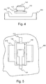
- Figures 4 and 5 illustrate a BAW with an etch pit structure.
- Figures 4 and 5 show the substrate 200, a membrane layer 130, the bottom electrode 110, the piezoelectric layer 100, and the top electrode 120.
- Figure 4 presents a sectional view of the structure, while Figure 5 shows a top view of the structure.
- the etch pit 210 is etched under the BAW structure after deposition of at least the membrane layer 130.
- Figure 6 illustrates another way of producing a bridge structure.
- a sacrificial layer 140 is deposited and patterned first.
- the rest of the BAW structure is deposited and patterned partly on top of the sacrificial layer 140.
- the sacrificial layer 140 is etched away.
- Figure 6 shows also the substrate 200, a membrane layer 130, the bottom electrode 110, the piezoelectric layer 100, and the top electrode 120.
- the sacrificial layer is preferably realized using a metal or a polymer as the material.
- the sacrificial layer may be produced using copper (Cu) as the material.
- the polymer is preferably such a polymer, which can withstand the relatively high temperatures, that can be reached during the deposition of the other layers.
- the polymer may be, by example, polytetrafluoroethylene or a derivative thereof, polyphenylene sulfide, polyetheretherketone, poly(para phenylene benzobismidazole) poly(para phenylene benzobisoxazole), poly (para phenylene benzobismidazole), poly(para phenylene benzobisthiazole), a polyimide, polyimide siloxane, vinyle ethers, polyphenyl, parylene-n, parylene-f, or benzocyclobutene.
- the sacrificial layer may be formed of any other material used in prior art, such as zinc oxide (ZnO). However, the use of a metal or a polymer is preferred as described previously.
- the resonator is acoustically isolated from the substrate by etching away the substrate from under a major portion of the BAW resonator structure.
- Figure 7 illustrates a via-hole structure of a BAW resonator.
- Figure 7 shows the substrate 200, a membrane layer 130, the bottom electrode 110, the piezoelectric layer 100, and the top electrode 120.
- a via-hole 211 has been etched through the whole substrate. Due to the etching required, via-hole structures are commonly realized only with Si or GaAs substrates.
- a further way to isolate a BAW resonator from the substrate is by using an acoustical mirror structure.
- the acoustical mirror structure performs the isolation by reflecting the acoustic wave back to the resonator structure.
- An acoustical mirror typically comprise several layers having a thickness of one quarter wavelength at the center frequency, alternating layers having differing acoustical impedances.
- the number of layers in an acoustic mirror is an odd integer, typically ranging from three to nine.
- the ratio of acoustic impedance of two consecutive layers should be large in order to present as low acoustic impedance as possible to the BAW resonator, instead of the relatively high impedance of the substrate material.
- the material of the high impedance layers can be for example gold (Au), molybdenum (Mo), or tungsten (W), and the material of the low impedance layers can be for example silicon (Si), polysilicon (poly-Si), silicon dioxide (SiO 2 ), aluminum (Al), or a polymer. Since in structures utilizing an acoustical mirror structure, the resonator is isolated from the substrate and the substrate is not modified very much, a wide variety of materials can be used as a substrate.
- the polymer layer may be comprised of any polymer material having a low loss characteristic and a low acoustic impedance.
- the polymer material is such that it can withstand temperatures of at least 350 °C, since relatively high temperatures may be achieved during deposition of other layers of the acoustical mirror structure and other structures.
- the polymer layer may be comprised of, by example, polyimide, cyclotene, a carbon-based material, a silicon-based material or any other suitable material.
- Figure 8 shows an example of a BAW resonator on top of an acoustical mirror structure.
- Figure 8 shows the substrate 200, the bottom electrode 110, the piezoelectric layer 100, and the top electrode 120.
- the acoustical mirror structure 150 comprises in this example three layers 150a, 150b. Two of the layers 150a are formed of a first material, and the third layer 150b in between the two layers is formed from a second material.
- the first and second materials have different acoustical impedances as described previously. The order of the materials can be different in different embodiments of the invention.
- the material with a high acoustical impedance can be in the middle and the material with a low acoustical impedance on both sides of the middle material.
- the order can be opposite.
- the bottom electrode may in some embodiments of the invention function as one layer of the acoustical mirror.
- Figure 9 shows a further BAW resonator structure according to an advantageous embodiment of the invention.
- Figure 9 shows a stacked resonator structure having two piezoelectric layers 100.
- a stacked structure requires a middle electrode 115, which is connected to ground potential.
- Figure 9 further shows the membrane layer 130, the substrate 200 and the etch pit 210 isolating the structure from the substrate.
- micromechanical switches are used to perform switching of signals to and from bulk acoustic wave resonators and surface acoustic wave resonators.
- Any micromechanical switch structures such as those similar to the structure presented in Figure 3, can be used in a structure according to the invention.
- More complicated switch structures such as multipole switches can be produced by combining more than one basic switches of Figure 3 and controlling them in a desired way to produce the desired switch function.
- Figure 13 One example of a more complicated switch structure is shown in Figure 13, which is described later in this specification.
- the switch elements and the resonator elements are fabricated during the same process, whereby the switch and resonator elements have layers, which are fabricated during the same process steps.
- a metal layer deposited on the substrate may after subsequent patteming form one of the electrodes of a BAW resonator and one of the electrodes of a micromechanical switch.
- bridge type BAW resonators and micromechanical switches since the same process steps which are used for creating the bridge structures, can be used to create the micromechanical switch structure.
- the sacrificial layer under a bridge structure and the sacrificial layer under a switch cantilever, which sacrificial layers are etched away at a later stage can be part of a single patterned layer.
- the substrate is made of silicon (Si), gallium arsenide (GaAs) or some other material suitable for use as a substrate for integrated circuits
- other elements than switching transistors can be realized on the same substrate.
- other circuits such as amplifiers can be integrated on the same substrate, which allows integration of nearly all RF components of a mobile communication means on a single substrate.
- the resonator and switch structures according to the invention can be used, for example, to realize switched filter banks.
- a switched filter bank 301 according to the invention is shown in figure 10.
- the embodiment of figure 10 can be used for example in filtering of a narrow part of a transmission or a receiving band.
- the filter bank 301 comprises several passband filters 300 having relatively narrow passbands, whereby a portion of a band can be selected for operation by switching the filter with the desired center frequency into use.
- the switches 320 at the first port of the filters are used to select which filter is used. Since the passbands of adjacent filters overlap each other to some extent, it is very difficult to match the filters at the second filter port if all the other filters, i.e.
- unused filters are connected to the other port causing loading of the second port.
- the unused filters would present a frequency dependent reactance, which is seen as shunt reactance at the second port.
- This problem can be solved by using a second switch 320 to each filter, as is shown in figure 10.
- the switches at the second ports i.e. output ports of the filters, may not be needed.
- the filter bank structure of figure 10 can be used to limit the noise and disturbing signals which the receiver receives from a single receiving band. At the transmission side, such a filter bank can clean up noise generated by the transmission circuitry outside the desired transmission frequencies.
- a filter bank 301 can comprise one or more filters in various embodiments of the invention.
- Figure 10 shows an example only.
- a filter bank can be used to select between different operating bands, for example in a mobile communication means, which is arranged to communicate with more than one networks having differing operating bands.
- Figure 11 shows a structure according to such an embodiment.
- switches 320 are used only at the input port of the filters 300.
- the passbands of the two filters 300 are sufficiently far apart, that the shunt reactance presented to the output port of the filter in use does not affect the passband of the filter in use too much.
- the switches 320 at the input port of the filters are used to select the desired filter.
- the arrangement shown in figure 11 can be used in a receiver structure as well as in a transmitter structure.
- FIG. 12a, 12b, and 12c shows various filter structures, which can be used according to various embodiments of the invention.
- Figure 12a illustrates a filter constructed from several bulk acoustic wave resonators 300 having a single piezoelectric layer. Using several resonators in a ladder topology as shown in Figure 12a provides in most cases better filtering properties than using a single resonator only.
- Figure 12b shows a filter structure constructed with bulk acoustic wave resonators 300' with a stacked structure. The filter comprises series coupled resonators 300' with shunt inductors 307 between the resonators.
- Figure 12c shows a filter structure adapted for narrow bandwith operation.
- the structure is otherwise similar to the structure of Figure 12b, but instead of shunt inductors, shunt capacitors 308 are used.
- the structures of Figures 12a, 12b, and 12c can be used, for example, in switched filter bank structures such as those shown in Figures 10 and 11.
- Bulk acoustic wave resonators can be used for realizing filters as described previously. Bulk acoustic wave resonators can also be used as modulators for producing amplitude modulated signals and phase modulated signals.
- the properties such as the resonance frequencies of the resonator change slightly, if a substantially constant voltage is applied between the electrodes, since the frequency response of the resonator is different when the resonator is bent in one direction than when the resonator is not bent. This property allows the creation of tunable resonators and filters. Further, this property can be used in modulator structures realized using bulk acoustic wave resonators.
- the modulating waveform Since the frequency of a modulating waveform is typically far below that of a radio frequency carrier, the modulating waveform forms a very slow-changing bias for the radio frequency carrier. Consequently, the resonance frequencies change in time according to the modulating waveform.
- the resonator When a radio frequency carrier having a frequency between the series and parallel resonance frequencies of the resonator is fed to the resonator, the resonator causes the RF carrier signal to be attenuated as a function of the modulating low frequency signal, producing amplitude modulation.
- the change of the properties of a bulk acoustic wave resonator can be used also in phase modulation. Since the phase shifting effect of a resonator has a sharp maximum at the resonance frequencies of the resonator, a change in the resonance frequencies of the resonator produces a substantially changing amount of phase shift for a radio frequency carrier having a frequency at or near an unmodulated resonance frequency of the resonator.
- Figure 13 illustrates one advantageous embodiment of the invention comprising bulk acoustic wave resonators used as modulators.
- Figure 13 shows the structure of a dual band modulator of a mobile communication means.
- the dual band modulator structure 500 receives a first radio frequency carrier from a first radio frequency carrier source 520, and a second radio frequency carrier from a second radio frequency carrier source 525. Both carriers are first band pass filtered in a band pass filter 300 constructed using a bulk acoustic wave resonator, after which both carrier signals are taken through a capacitor 505 which functions as a low frequency block to prevent the low frequency modulating signal from propagating to the band pass filters and carrier signal sources.
- the modulating low frequency signal is received from a modulating signal source 530.
- the modulating signal is low pass filtered in a low pass filter 535 and taken through an inductor 510, which functions as a high frequency block to prevent the carrier signals from propagating to the low pass filter and modulation signal source.
- the modulating signal is taken to a first switch block 320a comprising two micromechanical switches 320.
- the first switch block is used to select the carrier signal to be modulated.
- the modulating signal is lead to the first radio frequency carrier signal line or to the second radio frequency carrier signal line, and thereby to one of the modulators 315a, 315b.
- Figure 13 also illustrates two examples of possible resonator configurations in modulator use, i.e. a resonator coupled in series 315b and a resonator coupled in parallel 315a.
- a resonator coupled in series 315b In the series configuration, an inductor 515 is needed to provide a low frequency ground for the resonator 315b.
- a second switch block 320b is used to select the modulated signal for transmission.
- signal lines which control the position of switches 320 are not drawn in Figure 13.
- the dual band modulator structure components surrounded by the dashed line 500 can advantageously be manufactured on a single chip.
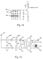
- Figure 14 shows a further advantageous embodiment of the invention.
- Figure 14 illustrates an oscillator circuit of the well known Colpitts type.
- a bulk acoustic wave resonator and switch bank 302 comprising micromechanical switches 320 and bulk acoustic wave resonators 300 is used for providing several operation frequencies for the oscillator circuit. The desired operating frequency is selected by selecting the corresponding resonator with one of the switches 320.
- This kind of an oscillator structure can advantageously be used, for example, in a multi-band mobile communication means. For clarity, signal lines which control the position of switches 320 are not drawn in Figure 14.
- Resonator and switch structures according to the invention can be used also in many other oscillator structures, and Figure 14 is shown as an example only. Since a Colpitts oscillator is well known by the man skilled in the art, the functioning and the structure of the oscillator in Figure 14 is not described here in further detail.
- FIG. 15 a block diagram of a mobile communication means according to a further advantageous embodiment of the invention is shown.
- the receiver part of the mobile communication means comprises a first receiver switched filter bank 302a for filtering the received signal, a receiver amplifier 605 for amplifying the received signal, a second receiver switched filter bank 302b for further filtering of the received signal, a mixer 610 for converting the received signal to baseband, a receiver block 630 for demodulating and decoding the signal and an earpiece 650 or a loudspeaker 650 for producing the audible received signal.
- the transmitter part comprises a microphone 656, a transmitter block 635 for coding the signal to be transmitted and performing other necessary signal processing, a modulator 615 for producing the modulated radio frequency signal, a first transmitter switched filter bank 302d, a transmitter amplifier 606, and a second transmitter switched filter bank 302c.
- the mobile communication means further comprises an antenna 601, an oscillator block 620, a control block 640, a display 652 and a keypad 654.
- the control block 640 controls the functioning of the receiver and transmitter blocks and the oscillator block, as well as displays information to the user via the display 652 and receives commands from the user via the keypad 654.
- the switched filter banks 302a, 302b, 302c, and 302d can have, for example, the structure shown in Figure 10 or the structure shown in Figure 11, or a structure which is a combination of the structures in Figures 10 and 11, depending on the width and the number of the operating bands of the mobile communication means. Other structures can also be used for the switched filter banks 302a, 302b, 302c, and 302d.
- the receiver switched filter banks 302a, 302b are used to limit the noise and disturbing signals which the receiver receives from a receiving band.
- the transmission switched filter banks 302c, 302d can clean up noise generated by the transmission circuitry outside the desired transmission frequencies.
- the oscillator block 620 may comprise an oscillator with a switched resonator bank, for example such as shown in Figure 14.
- the oscillator block 620 may further comprise a switched filter block for removing unwanted noise from the output of the oscillator circuit.
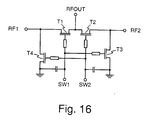
- the switches are realised with active semiconductor elements such as MESFET or MOSFET transistors or PIN diodes or other active switches having fast switching speed and low on-state resistance.
- Figure 16 shows an example of a MOSFET based switch structure, which can be used in an embodiment of the invention.
- the switch is an SP2T (single pole dual throat) switch.
- the switch has two RF inputs RF1, RF2 and one RF otput RFOUT, and two control inputs SW1, SW2.
- the state of the switch is chosen by applying a positive control voltage to one of the inputs SW1 and SW2 and a zero control voltage to the other.
- transistor T1 When transistor T1 is rendered into conductive stage by the control voltage, signal RF1 is passed to output RFOUT, while signal RF2 is shorted to ground via transistor T3.
- signal RF2 When transistor T2 is rendered into conductive stage by the control voltage, signal RF2 is passed to output RFOUT, while signal RF1 is shorted to ground via transistor T4. Since a man skilled in the art knows many other different transistor switch structures capable of operating at a high frequency, such structures are not described here in further detail.
- the substrate on which the resonator and switching means are deposited is used as a substrate, on which other components are attached.
- the substrate may provide wiring connections for other components, which wiring connections are realized as electrically conducting patterns on the substrate surface.
- Components such as integrated circuits can subsequently be bonded on the substrate.
- unpackaged integrated circuits can be bonded directly on the substrate using flip-chip bonding technique.
- Such an embodiment is especially advantageous, when glass is used as the substrate material, since the low cost of glass substrates allow relatively large substrates to be produced, whereby such substrates can accommodate other components in addition to the deposited resonator and switch structures.
- Resonator and switch structures according to the invention are advantageously used at frequencies roughly at or higher than 400 MHz, i.e. at frequencies where BAW resonators are feasible.
- the invention provides combined resonator and switch structures, which are economical to produce, since such structures can be produced in a single fabrication process.
- the invention further allows the production of complicated switched resonator and filter structures having a very small size, which is a substantial advantage in constructing multi-system mobile communication means.
- the resonators may be SAW or BAW resonators
- the switch elements may be transistors or micromechanical switches.
- a feature of the invention is, that the resonators and the switch elements have been prepared at least by deposition and patterning of a plurality of layers on the substrate.
- the present invention includes any novel feature or combination of features disclosed herein either explicitly or any generalisation thereof irrespective of whether or not it relates to the claimed invention or mitigates any or all of the problems addressed.
Abstract
Description
- The invention relates to resonator structures of radio communication apparatus.
- The development of mobile telecommunications continues towards ever smaller and increasingly complicated handheld units. The development has recently lead to new requirements for handheld units, namely that the units should support several different standards and telecommunications systems. Supporting several different systems requires several sets of filters and other RF components in the RF parts of the handheld units. Despite this complexity, the size of a handheld unit should not increase as a result of such a wide support.
- The RF filters used in prior art mobile phones are usually discrete surface acoustic wave (SAW) or ceramic filters. This approach has been adequate for single standard phones, but does not allow support of several telecommunications systems without increasing the size of a mobile phone.
- Surface acoustic wave (SAW) resonators typically have a structure similar to that shown in Figure 1. Surface acoustic resonators utilize surface acoustic vibration modes of a solid surface, in which modes the vibration is confined to the surface of the solid, decaying quickly away from the surface. A SAW resonator typically comprises a
piezoelectric layer 100, and twoelectrodes - It is known to construct thin film bulk acoustic wave resonators on semiconductor wafers, such as silicon (Si) or gallium arsenide (GaAs) wafers. For example, in an article entitled "Acoustic Bulk Wave Composite Resonators", Applied Physics Letters, Vol. 38, No. 3, pp. 125-127, Feb. 1, 1981, by K.M. Lakin and J.S. Wang, an acoustic bulk wave resonator is disclosed which comprises a thin film piezoelectric layers of zinc oxide (ZnO) sputtered over a thin membrane of silicon (Si). Further, in an article entitled "An Air-Gap Type Piezoelectric Composite Thin Film Resonator", 15 Proc. 39th Annual Symp. Freq. Control, pp. 361-366, 1985, by Hiroaki Satoh, Yasuo Ebata, Hitoshi Suzuki, and Choji Narahara, a bulk acoustic wave resonator having a bridge structure is disclosed.
- Figure 2 shows one example of a bulk acoustic wave resonator having a bridge structure. The structure comprises a
membrane 130 deposited on asubstrate 200. The resonator further comprises abottom electrode 110 on the membrane, apiezoelectric layer 100, and atop electrode 120. Agap 210 is created between the membrane and the substrate by etching away a sacrificial layer. The gap serves as an acoustic isolator, essentially isolating the vibrating resonator structure from the substrate. - Bulk acoustic wave resonators are not yet in widespread use, partly due to the reason that feasible ways of combining such resonators with other circuitry have not been presented. However, BAW resonators have some advantages as compared to SAW resonators. For example, BAW structures have a better tolerance of high power levels.
- Micromechanical devices are also presently under development. A micromechanical device is created typically on silicon substrates using deposition, patterning and etching techniques to create the desired structure. As an example, figure 3 illustrates the structure of a micromechanical switch. A micromechanical switch comprises a
cantilever 400,contact pads 430 on thesubstrate 200 and acontacting bar 440 for creating a contact between thecontact pads 430, and twoelectrodes cantilever electrode 410 is formed on the cantilever and thesubstrate electrode 420 on the substrate. The contacting bar is formed at one end of the cantilever, and the other end of the cantilever is fixed to the substrate, preferably with asupport 405 in order to raise the cantilever away from the substrate surface. The micromechanical switch is operated with a DC voltage coupled between the cantilever and substrate electrodes. The DC voltage creates an electrostatic force between the cantilever and substrate electrodes of the switch. The electrostatic force bends the cantilever, bringing the contacting bar into contact with thesubstrate contact pads 430. Various other micromechanical structures are disclosed in an article entitled "Ferroelectric Thin Films in Microelectromechanical Systems Applications", MRS Bulletin, July 1996, pp. 59 - 65, by D.L. Polla and L.F. Francis, and references contained therein. - According to the invention, at least one resonator structure and at least one switch structure are manufactured on the same substrate during the same process. This is especially advantageous when using bridge type BAW resonators and micromechanical switches, since the same process steps which are used for creating the bridge structures, can be used to create the micromechanical switch structure. Integration of switch structures and resonators on the same substrate allows the manufacture of very compact filter and resonator structures needed for multi-system mobile communication means.
- According to another aspect of the invention a special property of BAW resonators is utilized, namely that BAW resonators can be integrated on substrates which are commonly used for active circuitry, such as silicon (Si) and gallium arsenide (GaAs) surfaces. According to this aspect of the invention, the switches are realized with transistor structures using, for example, MESFET transistors.
- According to a first aspect of the present invention, there is provided a resonator structure comprising at least one resonator on a substrate, which resonator is prepared at least by deposition and patterning of a plurality of layers on the substrate, characterized in that the structure comprises at least one switch element prepared at least by deposition and patterning of a plurality of layers on the substrate.
- According to a second aspect of the present invention, there is provided a mobile communication means, characterized in that it comprises a resonator structure having at least one resonator on a substrate, which resonator is prepared at least by deposition and patterning of a plurality of layers on the substrate, and at least one switch element prepared at least by deposition and patterning of a plurality of layers on the substrate.
- An advantage of the invention is to enable the fabrication of structures allowing integration of bulk acoustic wave resonators with other circuitry in an advantageous way. Another advantage of the invention is to provide switched resonator structures. A further advantage of the invention is to provide such structures having a very small size. An advantage of the invention is to decrease the size of filter structures required for multi-system mobile communication means.
- These and other advantages are realised by integrating the resonator elements and the switch elements on the same substrate. Preferably, the resonator elements and the switch elements are integrated on the substrate during the same process.
- The invention is described in more detail in the following with reference to the accompanying drawings, of which
- Figure 1
- illustrates a surface acoustic resonator according to prior art,
- Figure 2
- illustrates a bulk acoustic wave resonator according to prior art,
- Figure 3
- illustrates a micromechanical switch structure according to prior art,
- Figure 4
- shows a sectional view of a bulk acoustic wave resonator having a bridge structure,
- Figure 5
- shows a top view of the structure in Figure 4,
- Figure 6
- shows another bulk acoustic wave resonator structure having a bridge structure,
- Figure 7
- illustrates a bulk acoustic wave resonator having a via-hole structure,
- Figure 8
- illustrates a bulk acoustic wave resonator isolated from the substrate by an acoustic mirror structure,
- Figure 9
- illustrates a bulk acoustic wave resonator having a stacked structure,
- Figure 10
- illustrates a switch and resonator structure according to the invention,
- Figure 11
- illustrates a further switch and resonator structure according to the invention,
- Figures 12a, 12b, and 12c
- illustrate various filter structures obtainable with bulk acoustic wave resonators,
- Figure 13
- illustrates the use of bulk acoustic wave resonators and micromechanical switches in a modulator structure according to the invention,
- Figure 14
- illustrates the use of bulk acoustic wave resonators and switch elements in oscillator structures,
- Figure 15
- illustrates the use of switched resonator banks in a mobile communication means according to the invention, and
- Figure 16
- illustrates a MOSFET transistor switch, which can be used in an advantageous embodiment of the invention.
- Same reference numerals are used for similar entities in the figures.
- According to the invention, switching means such as micromechanical switches and resonators are realized on a single substrate. The resonators are either surface acoustic wave (SAW) or bulk acoustic wave (BAW) resonators.
- Bulk acoustic wave resonators are typically fabricated on silicon (Si), gallium arsenide (GaAs), glass, or ceramic substrates. One ceramic substrate type, which is widely used, is alumina. The BAW devices are typically manufactured using various thin film manufacturing techniques, such as for example sputtering, vacuum evaporation or chemical vapour deposition. BAW devices utilize a piezoelectric thin film layer for generating the acoustic bulk waves. The resonance frequencies of typical BAW devices range from 0.5 Ghz to 5 Ghz, depending on the size and materials of the device. BAW resonators exhibit the typical series and parallel resonances of crystal resonators. The resonance frequencies are determined mainly by the material of the resonator and the dimensions of the layers of the resonator.
- A typical BAW resonator consists of three basic elements:
- an acoustically active piezoelectric layer,
- electrodes on opposite sides of the piezoelectric layer, and
- acoustical isolation from the substrate.
- The piezoelectric layer may be for example, ZnO, AIN, ZnS or any other piezoelectric material that can be fabricated as a thin film. As a further example, also ferroelectric ceramics can be used as the piezoelectric material. For example, PbTiO3 and Pb(ZrxTi1-x)O3 and other members of the so called lead lanthanum zirconate titanate family can be used.
- Preferably, the material used to form the electrode layers is an electrically conductive material having a high acoustic impedance. The electrodes may be comprised of for example any suitable metal, such as tungsten (W), aluminum (Al), copper (Cu), molybdenum (Mo), nickel (Ni), titanium (Ti), niobium (Nb), silver (Ag), gold (Au), and tantalum (Ta).
- The acoustical isolation can be produced with for example the following techniques:
- with a substrate via-hole,
- with a micromechanical bridge structure, or
- with an acoustic mirror structure.
- In the via-hole and bridge structures, the acoustically reflecting surfaces are the air interfaces below and above the devices. The bridge structure is typically manufactured using a sacrificial layer, which is etched away to produce a free-standing structure. Use of a sacrificial layer makes it possible to use a wide variety of substrate materials, since the substrate does not need to be modified very much, as in the via-hole structure.
- Bridge structures can be realized, for example, using an etch pit structure. Figures 4 and 5 illustrate a BAW with an etch pit structure. Figures 4 and 5 show the
substrate 200, amembrane layer 130, thebottom electrode 110, thepiezoelectric layer 100, and thetop electrode 120. Figure 4 presents a sectional view of the structure, while Figure 5 shows a top view of the structure. In the etch pit structure, theetch pit 210 is etched under the BAW structure after deposition of at least themembrane layer 130. - Figure 6 illustrates another way of producing a bridge structure. Before the deposition of other layers of the BAW structure, a
sacrificial layer 140 is deposited and patterned first. The rest of the BAW structure is deposited and patterned partly on top of thesacrificial layer 140. After the rest of the BAW structure is completed, thesacrificial layer 140 is etched away. Figure 6 shows also thesubstrate 200, amembrane layer 130, thebottom electrode 110, thepiezoelectric layer 100, and thetop electrode 120. - The sacrificial layer is preferably realized using a metal or a polymer as the material. For example, the sacrificial layer may be produced using copper (Cu) as the material. The polymer is preferably such a polymer, which can withstand the relatively high temperatures, that can be reached during the deposition of the other layers. The polymer may be, by example, polytetrafluoroethylene or a derivative thereof, polyphenylene sulfide, polyetheretherketone, poly(para phenylene benzobismidazole) poly(para phenylene benzobisoxazole), poly (para phenylene benzobismidazole), poly(para phenylene benzobisthiazole), a polyimide, polyimide siloxane, vinyle ethers, polyphenyl, parylene-n, parylene-f, or benzocyclobutene.
- The sacrificial layer may be formed of any other material used in prior art, such as zinc oxide (ZnO). However, the use of a metal or a polymer is preferred as described previously.
- In the via-hole structure, the resonator is acoustically isolated from the substrate by etching away the substrate from under a major portion of the BAW resonator structure. Figure 7 illustrates a via-hole structure of a BAW resonator. Figure 7 shows the
substrate 200, amembrane layer 130, thebottom electrode 110, thepiezoelectric layer 100, and thetop electrode 120. A via-hole 211 has been etched through the whole substrate. Due to the etching required, via-hole structures are commonly realized only with Si or GaAs substrates. - A further way to isolate a BAW resonator from the substrate is by using an acoustical mirror structure. The acoustical mirror structure performs the isolation by reflecting the acoustic wave back to the resonator structure. An acoustical mirror typically comprise several layers having a thickness of one quarter wavelength at the center frequency, alternating layers having differing acoustical impedances. The number of layers in an acoustic mirror is an odd integer, typically ranging from three to nine. The ratio of acoustic impedance of two consecutive layers should be large in order to present as low acoustic impedance as possible to the BAW resonator, instead of the relatively high impedance of the substrate material. The material of the high impedance layers can be for example gold (Au), molybdenum (Mo), or tungsten (W), and the material of the low impedance layers can be for example silicon (Si), polysilicon (poly-Si), silicon dioxide (SiO2), aluminum (Al), or a polymer. Since in structures utilizing an acoustical mirror structure, the resonator is isolated from the substrate and the substrate is not modified very much, a wide variety of materials can be used as a substrate.
- The polymer layer may be comprised of any polymer material having a low loss characteristic and a low acoustic impedance. Preferably, the polymer material is such that it can withstand temperatures of at least 350 °C, since relatively high temperatures may be achieved during deposition of other layers of the acoustical mirror structure and other structures. The polymer layer may be comprised of, by example, polyimide, cyclotene, a carbon-based material, a silicon-based material or any other suitable material.
- Figure 8 shows an example of a BAW resonator on top of an acoustical mirror structure. Figure 8 shows the
substrate 200, thebottom electrode 110, thepiezoelectric layer 100, and thetop electrode 120. Theacoustical mirror structure 150 comprises in this example threelayers layers 150a are formed of a first material, and thethird layer 150b in between the two layers is formed from a second material. The first and second materials have different acoustical impedances as described previously. The order of the materials can be different in different embodiments of the invention. In some embodiments of the invention, the material with a high acoustical impedance can be in the middle and the material with a low acoustical impedance on both sides of the middle material. In other embodiments of the invention, the order can be opposite. - The bottom electrode may in some embodiments of the invention function as one layer of the acoustical mirror.
- Figure 9 shows a further BAW resonator structure according to an advantageous embodiment of the invention. Figure 9 shows a stacked resonator structure having two
piezoelectric layers 100. In addition to the bottom 110 and top 120 electrodes, a stacked structure requires amiddle electrode 115, which is connected to ground potential. Figure 9 further shows themembrane layer 130, thesubstrate 200 and theetch pit 210 isolating the structure from the substrate. - For clarity, any passivation layers commonly needed for manufacturing microelectronic and micromechanical structures are not drawn in the figures of this specification.
- In one embodiment of the invention, micromechanical switches are used to perform switching of signals to and from bulk acoustic wave resonators and surface acoustic wave resonators. Any micromechanical switch structures, such as those similar to the structure presented in Figure 3, can be used in a structure according to the invention. More complicated switch structures such as multipole switches can be produced by combining more than one basic switches of Figure 3 and controlling them in a desired way to produce the desired switch function. One example of a more complicated switch structure is shown in Figure 13, which is described later in this specification.
- In an advantageous embodiment of the invention, the switch elements and the resonator elements are fabricated during the same process, whereby the switch and resonator elements have layers, which are fabricated during the same process steps. For example, a metal layer deposited on the substrate may after subsequent patteming form one of the electrodes of a BAW resonator and one of the electrodes of a micromechanical switch. This is especially advantageous when using bridge type BAW resonators and micromechanical switches, since the same process steps which are used for creating the bridge structures, can be used to create the micromechanical switch structure. For example, the sacrificial layer under a bridge structure and the sacrificial layer under a switch cantilever, which sacrificial layers are etched away at a later stage, can be part of a single patterned layer.
- In such an embodiment, in which the substrate is made of silicon (Si), gallium arsenide (GaAs) or some other material suitable for use as a substrate for integrated circuits, also other elements than switching transistors can be realized on the same substrate. For example, other circuits such as amplifiers can be integrated on the same substrate, which allows integration of nearly all RF components of a mobile communication means on a single substrate.
- The resonator and switch structures according to the invention can be used, for example, to realize switched filter banks. One possible application of a switched
filter bank 301 according to the invention is shown in figure 10. The embodiment of figure 10 can be used for example in filtering of a narrow part of a transmission or a receiving band. Thefilter bank 301 comprisesseveral passband filters 300 having relatively narrow passbands, whereby a portion of a band can be selected for operation by switching the filter with the desired center frequency into use. Theswitches 320 at the first port of the filters are used to select which filter is used. Since the passbands of adjacent filters overlap each other to some extent, it is very difficult to match the filters at the second filter port if all the other filters, i.e. unused filters, are connected to the other port causing loading of the second port. The unused filters would present a frequency dependent reactance, which is seen as shunt reactance at the second port. This problem can be solved by using asecond switch 320 to each filter, as is shown in figure 10. In such applications, where the passbands of the filters are relatively far apart, the switches at the second ports, i.e. output ports of the filters, may not be needed. The filter bank structure of figure 10 can be used to limit the noise and disturbing signals which the receiver receives from a single receiving band. At the transmission side, such a filter bank can clean up noise generated by the transmission circuitry outside the desired transmission frequencies. - A
filter bank 301 can comprise one or more filters in various embodiments of the invention. Figure 10 shows an example only. - In an another advantageous embodiment of the invention, a filter bank can be used to select between different operating bands, for example in a mobile communication means, which is arranged to communicate with more than one networks having differing operating bands. Figure 11 shows a structure according to such an embodiment. In figure 11,
switches 320 are used only at the input port of thefilters 300. In this example, the passbands of the twofilters 300 are sufficiently far apart, that the shunt reactance presented to the output port of the filter in use does not affect the passband of the filter in use too much. Theswitches 320 at the input port of the filters are used to select the desired filter. The arrangement shown in figure 11 can be used in a receiver structure as well as in a transmitter structure. - Filters that utilize bulk acoustic wave resonators can comprise more than one resonator. Figures 12a, 12b, and 12c shows various filter structures, which can be used according to various embodiments of the invention. Figure 12a illustrates a filter constructed from several bulk
acoustic wave resonators 300 having a single piezoelectric layer. Using several resonators in a ladder topology as shown in Figure 12a provides in most cases better filtering properties than using a single resonator only. Figure 12b shows a filter structure constructed with bulk acoustic wave resonators 300' with a stacked structure. The filter comprises series coupled resonators 300' withshunt inductors 307 between the resonators. Figure 12c shows a filter structure adapted for narrow bandwith operation. The structure is otherwise similar to the structure of Figure 12b, but instead of shunt inductors,shunt capacitors 308 are used. The structures of Figures 12a, 12b, and 12c can be used, for example, in switched filter bank structures such as those shown in Figures 10 and 11. - Bulk acoustic wave resonators can be used for realizing filters as described previously. Bulk acoustic wave resonators can also be used as modulators for producing amplitude modulated signals and phase modulated signals. The properties such as the resonance frequencies of the resonator change slightly, if a substantially constant voltage is applied between the electrodes, since the frequency response of the resonator is different when the resonator is bent in one direction than when the resonator is not bent. This property allows the creation of tunable resonators and filters. Further, this property can be used in modulator structures realized using bulk acoustic wave resonators. Since the frequency of a modulating waveform is typically far below that of a radio frequency carrier, the modulating waveform forms a very slow-changing bias for the radio frequency carrier. Consequently, the resonance frequencies change in time according to the modulating waveform. When a radio frequency carrier having a frequency between the series and parallel resonance frequencies of the resonator is fed to the resonator, the resonator causes the RF carrier signal to be attenuated as a function of the modulating low frequency signal, producing amplitude modulation.
- The change of the properties of a bulk acoustic wave resonator can be used also in phase modulation. Since the phase shifting effect of a resonator has a sharp maximum at the resonance frequencies of the resonator, a change in the resonance frequencies of the resonator produces a substantially changing amount of phase shift for a radio frequency carrier having a frequency at or near an unmodulated resonance frequency of the resonator.
- Figure 13 illustrates one advantageous embodiment of the invention comprising bulk acoustic wave resonators used as modulators. Figure 13 shows the structure of a dual band modulator of a mobile communication means. The dual
band modulator structure 500 receives a first radio frequency carrier from a first radiofrequency carrier source 520, and a second radio frequency carrier from a second radiofrequency carrier source 525. Both carriers are first band pass filtered in aband pass filter 300 constructed using a bulk acoustic wave resonator, after which both carrier signals are taken through acapacitor 505 which functions as a low frequency block to prevent the low frequency modulating signal from propagating to the band pass filters and carrier signal sources. - The modulating low frequency signal is received from a modulating
signal source 530. The modulating signal is low pass filtered in alow pass filter 535 and taken through aninductor 510, which functions as a high frequency block to prevent the carrier signals from propagating to the low pass filter and modulation signal source. From theinductor 510, the modulating signal is taken to afirst switch block 320a comprising twomicromechanical switches 320. The first switch block is used to select the carrier signal to be modulated. Depending on the position of the two switches of the first switch block, the modulating signal is lead to the first radio frequency carrier signal line or to the second radio frequency carrier signal line, and thereby to one of the modulators 315a, 315b. Figure 13 also illustrates two examples of possible resonator configurations in modulator use, i.e. a resonator coupled inseries 315b and a resonator coupled in parallel 315a. In the series configuration, aninductor 515 is needed to provide a low frequency ground for theresonator 315b. Asecond switch block 320b is used to select the modulated signal for transmission. For clarity, signal lines which control the position ofswitches 320 are not drawn in Figure 13. The dual band modulator structure components surrounded by the dashedline 500 can advantageously be manufactured on a single chip. - Figure 14 shows a further advantageous embodiment of the invention. Figure 14 illustrates an oscillator circuit of the well known Colpitts type. A bulk acoustic wave resonator and
switch bank 302 comprisingmicromechanical switches 320 and bulkacoustic wave resonators 300 is used for providing several operation frequencies for the oscillator circuit. The desired operating frequency is selected by selecting the corresponding resonator with one of theswitches 320. This kind of an oscillator structure can advantageously be used, for example, in a multi-band mobile communication means. For clarity, signal lines which control the position ofswitches 320 are not drawn in Figure 14. Resonator and switch structures according to the invention can be used also in many other oscillator structures, and Figure 14 is shown as an example only. Since a Colpitts oscillator is well known by the man skilled in the art, the functioning and the structure of the oscillator in Figure 14 is not described here in further detail. - In Figure 15, a block diagram of a mobile communication means according to a further advantageous embodiment of the invention is shown. The receiver part of the mobile communication means comprises a first receiver switched
filter bank 302a for filtering the received signal, areceiver amplifier 605 for amplifying the received signal, a second receiver switchedfilter bank 302b for further filtering of the received signal, amixer 610 for converting the received signal to baseband, areceiver block 630 for demodulating and decoding the signal and anearpiece 650 or aloudspeaker 650 for producing the audible received signal. The transmitter part comprises amicrophone 656, atransmitter block 635 for coding the signal to be transmitted and performing other necessary signal processing, amodulator 615 for producing the modulated radio frequency signal, a first transmitter switchedfilter bank 302d, atransmitter amplifier 606, and a second transmitter switchedfilter bank 302c. The mobile communication means further comprises anantenna 601, anoscillator block 620, acontrol block 640, adisplay 652 and akeypad 654. Thecontrol block 640 controls the functioning of the receiver and transmitter blocks and the oscillator block, as well as displays information to the user via thedisplay 652 and receives commands from the user via thekeypad 654. The switchedfilter banks filter banks filter banks filter banks oscillator block 620 may comprise an oscillator with a switched resonator bank, for example such as shown in Figure 14. Theoscillator block 620 may further comprise a switched filter block for removing unwanted noise from the output of the oscillator circuit. - In an advantageous embodiment of the invention, the switches are realised with active semiconductor elements such as MESFET or MOSFET transistors or PIN diodes or other active switches having fast switching speed and low on-state resistance. Figure 16 shows an example of a MOSFET based switch structure, which can be used in an embodiment of the invention. The switch is an SP2T (single pole dual throat) switch. The switch has two RF inputs RF1, RF2 and one RF otput RFOUT, and two control inputs SW1, SW2. The state of the switch is chosen by applying a positive control voltage to one of the inputs SW1 and SW2 and a zero control voltage to the other. When transistor T1 is rendered into conductive stage by the control voltage, signal RF1 is passed to output RFOUT, while signal RF2 is shorted to ground via transistor T3. When transistor T2 is rendered into conductive stage by the control voltage, signal RF2 is passed to output RFOUT, while signal RF1 is shorted to ground via transistor T4. Since a man skilled in the art knows many other different transistor switch structures capable of operating at a high frequency, such structures are not described here in further detail.
- According to a further advantageous embodiment of the invention, the substrate on which the resonator and switching means are deposited is used as a substrate, on which other components are attached. For example, the substrate may provide wiring connections for other components, which wiring connections are realized as electrically conducting patterns on the substrate surface. Components such as integrated circuits can subsequently be bonded on the substrate. For example, unpackaged integrated circuits can be bonded directly on the substrate using flip-chip bonding technique. Such an embodiment is especially advantageous, when glass is used as the substrate material, since the low cost of glass substrates allow relatively large substrates to be produced, whereby such substrates can accommodate other components in addition to the deposited resonator and switch structures.
- Resonator and switch structures according to the invention are advantageously used at frequencies roughly at or higher than 400 MHz, i.e. at frequencies where BAW resonators are feasible.
- The invention provides combined resonator and switch structures, which are economical to produce, since such structures can be produced in a single fabrication process. The invention further allows the production of complicated switched resonator and filter structures having a very small size, which is a substantial advantage in constructing multi-system mobile communication means.
- In view of the foregoing description it will be evident to a person skilled in the art that various modifications may be made within the scope of the invention. While a preferred embodiment of the invention has been described in detail, it should be apparent that many modifications and variations thereto are possible, all of which fall within the true spirit and scope of the invention. For example, the resonators may be SAW or BAW resonators, and the switch elements may be transistors or micromechanical switches. A feature of the invention is, that the resonators and the switch elements have been prepared at least by deposition and patterning of a plurality of layers on the substrate.
- The present invention includes any novel feature or combination of features disclosed herein either explicitly or any generalisation thereof irrespective of whether or not it relates to the claimed invention or mitigates any or all of the problems addressed.
Claims (11)
- A resonator structure comprising at least one resonator on a substrate, which resonator is prepared at least by deposition and patterning of a plurality of layers on the substrate, characterized in that the structure comprises at least one switch element prepared at least by deposition and patterning of a plurality of layers on the substrate.
- A resonator structure according to claim 1, characterized in that at least one of said at least one switch element has at least one transistor.
- A resonator structure according to claim 1, characterized in that at least one of said at least one switch element is a micromechanical switch.
- A resonator structure according to claim 1, characterized in that at least one of the at least one resonator is a bulk acoustic wave resonator.
- A resonator structure according to claim 1, characterized in that at least one of the at least one resonator is a surface acoustic wave resonator.
- A resonator structure according to claim 1, characterized in that at least one of the at least one resonator has at least one layer, which is a part of the same layer, of which at least one layer of at least one of said at least one switch elements is a part of.
- A resonator structure according to claim 1, characterized in that the resonator structure comprises at least one filter.
- A resonator structure according to claim 1, characterized in that the resonator structure comprises at least one modulator.
- A resonator structure according to claim 1, characterized in that the resonator structure is a switched resonator bank of a switched filter bank.
- A resonator structure according to claim 1, characterized in that at least one transistor is integrated on the substrate.
- A mobile communication means, characterized in that it comprisesa resonator structure having at least one resonator on a substrate, which resonator is prepared at least by deposition and patterning of a plurality of layers on the substrate, andat least one switch element prepared at least by deposition and patterning of a plurality of layers on the substrate.
Priority Applications (1)
| Application Number | Priority Date | Filing Date | Title |
|---|---|---|---|
| EP08004288A EP1936733B1 (en) | 1998-06-02 | 1999-06-02 | Resonator structures |
Applications Claiming Priority (2)
| Application Number | Priority Date | Filing Date | Title |
|---|---|---|---|
| FI981245 | 1998-06-02 | ||
| FI981245A FI106894B (en) | 1998-06-02 | 1998-06-02 | resonator structures |
Related Child Applications (1)
| Application Number | Title | Priority Date | Filing Date |
|---|---|---|---|
| EP08004288A Division EP1936733B1 (en) | 1998-06-02 | 1999-06-02 | Resonator structures |
Publications (2)
| Publication Number | Publication Date |
|---|---|
| EP0962999A2 true EP0962999A2 (en) | 1999-12-08 |
| EP0962999A3 EP0962999A3 (en) | 2001-05-16 |
Family
ID=8551881
Family Applications (2)
| Application Number | Title | Priority Date | Filing Date |
|---|---|---|---|
| EP08004288A Expired - Lifetime EP1936733B1 (en) | 1998-06-02 | 1999-06-02 | Resonator structures |
| EP99304277A Ceased EP0962999A3 (en) | 1998-06-02 | 1999-06-02 | Resonator structures |
Family Applications Before (1)
| Application Number | Title | Priority Date | Filing Date |
|---|---|---|---|
| EP08004288A Expired - Lifetime EP1936733B1 (en) | 1998-06-02 | 1999-06-02 | Resonator structures |
Country Status (5)
| Country | Link |
|---|---|
| US (1) | US6242843B1 (en) |
| EP (2) | EP1936733B1 (en) |
| JP (1) | JP2000030594A (en) |
| CN (1) | CN1130790C (en) |
| FI (1) | FI106894B (en) |
Cited By (20)
| Publication number | Priority date | Publication date | Assignee | Title |
|---|---|---|---|---|
| WO2001056153A1 (en) * | 2000-01-28 | 2001-08-02 | Infineon Technologies Ag | Circuit arrangement with band-pass filters |
| EP1126602A2 (en) | 2000-02-18 | 2001-08-22 | Infineon Technologies AG | Piezoelectric resonator |
| WO2001082467A2 (en) * | 2000-04-20 | 2001-11-01 | The Regents Of The University Of Michigan | Method and apparatus for generating a signal having at least one desired output frequency utilizing a bank of vibrating micromechanical devices |
| WO2001097375A1 (en) * | 2000-06-16 | 2001-12-20 | Koninklijke Philips Electronics N.V. | Bulk accoustic wave filter |
| WO2002079079A1 (en) * | 2001-04-02 | 2002-10-10 | Telefonaktiebolaget Lm Ericsson (Publ) | Micro electromechanical switches |
| WO2002087081A1 (en) * | 2001-04-25 | 2002-10-31 | Koninklijke Philips Electronics N.V. | Arrangement with two piezoelectric layers, and method of operating a filter device |
| US6566786B2 (en) | 1999-01-14 | 2003-05-20 | The Regents Of The University Of Michigan | Method and apparatus for selecting at least one desired channel utilizing a bank of vibrating micromechanical apparatus |
| US6577040B2 (en) | 1999-01-14 | 2003-06-10 | The Regents Of The University Of Michigan | Method and apparatus for generating a signal having at least one desired output frequency utilizing a bank of vibrating micromechanical devices |
| US6593831B2 (en) | 1999-01-14 | 2003-07-15 | The Regents Of The University Of Michigan | Method and apparatus for filtering signals in a subsystem including a power amplifier utilizing a bank of vibrating micromechanical apparatus |
| US6600252B2 (en) | 1999-01-14 | 2003-07-29 | The Regents Of The University Of Michigan | Method and subsystem for processing signals utilizing a plurality of vibrating micromechanical devices |
| US6621368B2 (en) | 2001-06-06 | 2003-09-16 | Remec Oy | Dynamic range extension for an electronic circuit |
| GB2367436B (en) * | 2000-05-08 | 2004-02-04 | Agilent Technologies Inc | Acoustic resonator |
| WO2004011366A1 (en) * | 2002-07-30 | 2004-02-05 | Sony Corporation | Micromachine and method of manufacturing the micromachine |
| US6788170B1 (en) | 1999-07-19 | 2004-09-07 | Nokia Corporation | Resonator structure having a dampening material and a filter having such a resonator structure |
| WO2005076480A1 (en) * | 2004-02-03 | 2005-08-18 | Nokia Corporation | Reference oscillator frequency stabilization |
| US7230510B2 (en) | 2002-11-19 | 2007-06-12 | Nxp B. V. | Duplexer and method of isolating an Rx-band and a Tx-band |
| US7378781B2 (en) | 2005-09-07 | 2008-05-27 | Nokia Corporation | Acoustic wave resonator with integrated temperature control for oscillator purposes |
| DE102008049668B4 (en) * | 2008-09-30 | 2016-05-04 | Intel Deutschland Gmbh | High-frequency pre-amplifier and receiver |
| CN108390661A (en) * | 2017-02-03 | 2018-08-10 | 三星电机株式会社 | Filter and front-end module including filter |
| CN108390660A (en) * | 2017-02-03 | 2018-08-10 | 三星电机株式会社 | Filter |
Families Citing this family (53)
| Publication number | Priority date | Publication date | Assignee | Title |
|---|---|---|---|---|
| FI108583B (en) * | 1998-06-02 | 2002-02-15 | Nokia Corp | resonator structures |
| JP2000209063A (en) * | 1998-11-12 | 2000-07-28 | Mitsubishi Electric Corp | Thin film piezoelectric element |
| WO2001043153A1 (en) * | 1999-12-10 | 2001-06-14 | Koninklijke Philips Electronics N.V. | Electronic devices including micromechanical switches |
| CN1383610B (en) * | 2000-04-06 | 2010-05-26 | Nxp股份有限公司 | Tunable filter arrangement comprising resonator |
| US7394430B2 (en) * | 2001-04-11 | 2008-07-01 | Kyocera Wireless Corp. | Wireless device reconfigurable radiation desensitivity bracket systems and methods |
| US7221243B2 (en) * | 2001-04-11 | 2007-05-22 | Kyocera Wireless Corp. | Apparatus and method for combining electrical signals |
| US7154440B2 (en) * | 2001-04-11 | 2006-12-26 | Kyocera Wireless Corp. | Phase array antenna using a constant-gain phase shifter |
| US6690251B2 (en) * | 2001-04-11 | 2004-02-10 | Kyocera Wireless Corporation | Tunable ferro-electric filter |
| US7746292B2 (en) * | 2001-04-11 | 2010-06-29 | Kyocera Wireless Corp. | Reconfigurable radiation desensitivity bracket systems and methods |
| US7174147B2 (en) * | 2001-04-11 | 2007-02-06 | Kyocera Wireless Corp. | Bandpass filter with tunable resonator |
| FI118400B (en) * | 2001-08-21 | 2007-10-31 | Nokia Corp | Filter structure comprising piezoelectric resonators |
| US7184727B2 (en) * | 2002-02-12 | 2007-02-27 | Kyocera Wireless Corp. | Full-duplex antenna system and method |
| US7176845B2 (en) * | 2002-02-12 | 2007-02-13 | Kyocera Wireless Corp. | System and method for impedance matching an antenna to sub-bands in a communication band |
| US7180467B2 (en) * | 2002-02-12 | 2007-02-20 | Kyocera Wireless Corp. | System and method for dual-band antenna matching |
| KR100499126B1 (en) * | 2002-06-20 | 2005-07-04 | 삼성전자주식회사 | Actuator using organic film membrane |
| US6944432B2 (en) * | 2002-11-12 | 2005-09-13 | Nokia Corporation | Crystal-less oscillator transceiver |
| FR2852165A1 (en) * | 2003-03-06 | 2004-09-10 | St Microelectronics Sa | PROCESS FOR PRODUCING A TUNABLE PIEZOLECTRIC MICRORESONATOR |
| JP2004281742A (en) * | 2003-03-17 | 2004-10-07 | Japan Science & Technology Agency | Semiconductor device, semiconductor sensor and semiconductor memory element |
| KR100599083B1 (en) * | 2003-04-22 | 2006-07-12 | 삼성전자주식회사 | Cantilevered type Film Bulk Acoustic Resonator fabrication method and Resonator fabricated by the same |
| US6927651B2 (en) * | 2003-05-12 | 2005-08-09 | Agilent Technologies, Inc. | Acoustic resonator devices having multiple resonant frequencies and methods of making the same |
| US20040227578A1 (en) * | 2003-05-14 | 2004-11-18 | Miikka Hamalainen | Acoustic resonance-based frequency synthesizer using at least one bulk acoustic wave (BAW) or thin film bulk acoustic wave (FBAR) device |
| US7720443B2 (en) | 2003-06-02 | 2010-05-18 | Kyocera Wireless Corp. | System and method for filtering time division multiple access telephone communications |
| US6862441B2 (en) * | 2003-06-09 | 2005-03-01 | Nokia Corporation | Transmitter filter arrangement for multiband mobile phone |
| US7196591B2 (en) * | 2003-08-06 | 2007-03-27 | Synergy Microwave Corporation | Tunable frequency, low phase noise and low thermal drift oscillator |
| JP2005136588A (en) * | 2003-10-29 | 2005-05-26 | Sharp Corp | Piezoelectric thin film resonator, filter, filter bank, filter bank integrated power amplifier, and high-frequency communication apparatus |
| DE10352642B4 (en) * | 2003-11-11 | 2018-11-29 | Snaptrack, Inc. | Circuit with reduced insertion loss and device with the circuit |
| US20050148065A1 (en) | 2003-12-30 | 2005-07-07 | Intel Corporation | Biosensor utilizing a resonator having a functionalized surface |
| US7248845B2 (en) * | 2004-07-09 | 2007-07-24 | Kyocera Wireless Corp. | Variable-loss transmitter and method of operation |
| EP1833172B1 (en) * | 2004-12-28 | 2012-04-04 | Murata Manufacturing Co., Ltd. | Balance/unbalance filter module and communication apparatus |
| JP2006203304A (en) * | 2005-01-18 | 2006-08-03 | Hitachi Media Electoronics Co Ltd | Piezoelectric thin-film resonator, oscillator using the same, and semiconductor integrated circuit containing the same |
| US8238074B2 (en) * | 2005-05-02 | 2012-08-07 | Epcos Ag | Capacitive RF-MEMS device with integrated decoupling capacitor |
| US7636021B2 (en) * | 2005-05-20 | 2009-12-22 | Synergy Microwave Corporation | Low noise and low phase hits tunable oscillator |
| US20060273866A1 (en) * | 2005-06-07 | 2006-12-07 | Nokia Corporation | Film bulk acoustic wave resonator with differential topology |
| US7299529B2 (en) * | 2005-06-16 | 2007-11-27 | Intel Corporation | Film bulk acoustic resonator (FBAR) process using single-step resonator layer deposition |
| US20070089513A1 (en) * | 2005-09-30 | 2007-04-26 | Rosenau Steven A | Resonator based transmitters for capacitive sensors |
| US8008993B2 (en) * | 2005-09-30 | 2011-08-30 | Nxp B.V. | Thin-film bulk-acoustic wave (BAW) resonators |
| CA2568244C (en) * | 2005-11-15 | 2009-08-11 | Synergy Microwave Corporation | User-definable, low cost, low noise, and phase hit insensitive multi-octave-bandtunable oscillator |
| US7548762B2 (en) * | 2005-11-30 | 2009-06-16 | Kyocera Corporation | Method for tuning a GPS antenna matching network |
| JP2007174438A (en) | 2005-12-23 | 2007-07-05 | Toshiba Corp | Filter circuit and radio communication system with filter |
| US7675388B2 (en) * | 2006-03-07 | 2010-03-09 | Agile Rf, Inc. | Switchable tunable acoustic resonator using BST material |
| DE102006023165B4 (en) * | 2006-05-17 | 2008-02-14 | Infineon Technologies Ag | Method for producing an acoustic mirror from alternately arranged layers of high and low acoustic impedance |
| CN101115325B (en) * | 2006-07-28 | 2011-05-11 | 中国科学院声学研究所 | Frequency modulation silicon microcondenser microphone system suitable for single chip integration |
| EP1976015B1 (en) | 2007-03-26 | 2014-09-10 | Semiconductor Energy Laboratory Co., Ltd. | Switching element, method for manufacturing the same, and display device including switching element |
| JP5136134B2 (en) * | 2008-03-18 | 2013-02-06 | ソニー株式会社 | BANDPASS FILTER DEVICE, ITS MANUFACTURING METHOD, TELEVISION TUNER, AND TELEVISION RECEIVER |
| US7777595B2 (en) * | 2008-04-30 | 2010-08-17 | John Mezzalingua Associates, Inc. | Multi-channel filter assemblies |
| EP2332208B1 (en) * | 2008-09-08 | 2013-07-31 | Telefonaktiebolaget L M Ericsson (PUBL) | A reconfigurable filter apparatus |
| US20110076974A1 (en) * | 2009-01-31 | 2011-03-31 | Sei-Joo Jang | Flexible wireless network system and method of use |
| EP2922203A1 (en) * | 2010-12-10 | 2015-09-23 | Peregrine Semiconductor Corporation | Temperature and process compensated tunable acoustic wave filter |
| WO2015084456A2 (en) | 2013-09-18 | 2015-06-11 | The Regents Of The University Of California | Tunable q resonator |
| WO2019021983A1 (en) * | 2017-07-25 | 2019-01-31 | 株式会社村田製作所 | High frequency filter, multiplexer, high frequency front-end circuit, and communication device |
| CN111684718B (en) * | 2018-02-05 | 2023-07-25 | 株式会社村田制作所 | Filter device, high-frequency front-end circuit, and communication device |
| KR20200078084A (en) * | 2018-12-21 | 2020-07-01 | 삼성전기주식회사 | Front end module |
| US10979019B2 (en) * | 2019-06-11 | 2021-04-13 | Globalfoundries Singapore Pte. Ltd. | Reconfigurable resonator devices, methods of forming reconfigurable resonator devices, and operations thereof |
Citations (6)
| Publication number | Priority date | Publication date | Assignee | Title |
|---|---|---|---|---|
| US4570139A (en) * | 1984-12-14 | 1986-02-11 | Eaton Corporation | Thin-film magnetically operated micromechanical electric switching device |
| EP0709911A2 (en) * | 1994-10-31 | 1996-05-01 | Texas Instruments Incorporated | Improved switches |
| US5589082A (en) * | 1992-12-11 | 1996-12-31 | The Regents Of The University Of California | Microelectromechanical signal processor fabrication |
| US5714917A (en) * | 1996-10-02 | 1998-02-03 | Nokia Mobile Phones Limited | Device incorporating a tunable thin film bulk acoustic resonator for performing amplitude and phase modulation |
| EP0849820A2 (en) * | 1996-12-21 | 1998-06-24 | HE HOLDINGS, INC. dba HUGHES ELECTRONICS | Tunable microwave network using microelectromechanical switches |
| WO1999042282A1 (en) * | 1998-02-20 | 1999-08-26 | Advanced Technology Materials, Inc. | A-site and/or b-site modified pbzrtio3 materials and films |
Family Cites Families (11)
| Publication number | Priority date | Publication date | Assignee | Title |
|---|---|---|---|---|
| JPH03178206A (en) * | 1989-12-06 | 1991-08-02 | Nec Corp | Monolithic integrated circuit oscillator |
| US5075641A (en) * | 1990-12-04 | 1991-12-24 | Iowa State University Research Foundation, Inc. | High frequency oscillator comprising cointegrated thin film resonator and active device |
| US5747857A (en) * | 1991-03-13 | 1998-05-05 | Matsushita Electric Industrial Co., Ltd. | Electronic components having high-frequency elements and methods of manufacture therefor |
| JPH0546111U (en) * | 1991-11-21 | 1993-06-18 | 三菱電機株式会社 | Surface acoustic wave oscillator |
| JPH06125A (en) * | 1992-06-22 | 1994-01-11 | Matsushita Electric Ind Co Ltd | Rice cooker |
| JPH07109816B2 (en) * | 1992-10-13 | 1995-11-22 | 松下電器産業株式会社 | Electro-acoustic integrated circuit and manufacturing method thereof |
| US5382930A (en) | 1992-12-21 | 1995-01-17 | Trw Inc. | Monolithic multipole filters made of thin film stacked crystal filters |
| US5373268A (en) | 1993-02-01 | 1994-12-13 | Motorola, Inc. | Thin film resonator having stacked acoustic reflecting impedance matching layers and method |
| JPH08148968A (en) * | 1994-11-24 | 1996-06-07 | Mitsubishi Electric Corp | Thin film piezoelectric element |
| US5873154A (en) | 1996-10-17 | 1999-02-23 | Nokia Mobile Phones Limited | Method for fabricating a resonator having an acoustic mirror |
| US5872493A (en) | 1997-03-13 | 1999-02-16 | Nokia Mobile Phones, Ltd. | Bulk acoustic wave (BAW) filter having a top portion that includes a protective acoustic mirror |
-
1998
- 1998-06-02 FI FI981245A patent/FI106894B/en not_active IP Right Cessation
-
1999
- 1999-05-27 US US09/321,339 patent/US6242843B1/en not_active Expired - Lifetime
- 1999-06-02 EP EP08004288A patent/EP1936733B1/en not_active Expired - Lifetime
- 1999-06-02 CN CN99106965A patent/CN1130790C/en not_active Expired - Fee Related
- 1999-06-02 JP JP11154477A patent/JP2000030594A/en active Pending
- 1999-06-02 EP EP99304277A patent/EP0962999A3/en not_active Ceased
Patent Citations (6)
| Publication number | Priority date | Publication date | Assignee | Title |
|---|---|---|---|---|
| US4570139A (en) * | 1984-12-14 | 1986-02-11 | Eaton Corporation | Thin-film magnetically operated micromechanical electric switching device |
| US5589082A (en) * | 1992-12-11 | 1996-12-31 | The Regents Of The University Of California | Microelectromechanical signal processor fabrication |
| EP0709911A2 (en) * | 1994-10-31 | 1996-05-01 | Texas Instruments Incorporated | Improved switches |
| US5714917A (en) * | 1996-10-02 | 1998-02-03 | Nokia Mobile Phones Limited | Device incorporating a tunable thin film bulk acoustic resonator for performing amplitude and phase modulation |
| EP0849820A2 (en) * | 1996-12-21 | 1998-06-24 | HE HOLDINGS, INC. dba HUGHES ELECTRONICS | Tunable microwave network using microelectromechanical switches |
| WO1999042282A1 (en) * | 1998-02-20 | 1999-08-26 | Advanced Technology Materials, Inc. | A-site and/or b-site modified pbzrtio3 materials and films |
Non-Patent Citations (2)
| Title |
|---|
| LAKIN K M ET AL: "ACOUSTIC BULK WAVE COMPOSITE RESONATORS" APPLIED PHYSICS LETTERS,US,AMERICAN INSTITUTE OF PHYSICS. NEW YORK, vol. 38, no. 3, 1 February 1981 (1981-02-01), pages 125-127, XP000647247 ISSN: 0003-6951 * |
| SATOH H ET AL: "AN AIR-GAP TYPE PIEZOELECTRIC COMPOSITE THIN FILM RESONATOR" PROCEEDINGS OF THE ANNUAL FREQUENCY CONTROL SYMPOSIUM,US,NEW YORK, IEEE, vol. SYMP. 39, 29 May 1985 (1985-05-29), pages 361-366, XP000647260 * |
Cited By (36)
| Publication number | Priority date | Publication date | Assignee | Title |
|---|---|---|---|---|
| US6917138B2 (en) | 1999-01-14 | 2005-07-12 | The Regents Of The University Of Michigan | Method and subsystem for processing signals utilizing a plurality of vibrating micromechanical devices |
| US6680660B2 (en) | 1999-01-14 | 2004-01-20 | The Regents Of The University Of Michigan | Method and apparatus for selecting at least one desired channel utilizing a bank of vibrating micromechanical apparatus |
| US6600252B2 (en) | 1999-01-14 | 2003-07-29 | The Regents Of The University Of Michigan | Method and subsystem for processing signals utilizing a plurality of vibrating micromechanical devices |
| US6593831B2 (en) | 1999-01-14 | 2003-07-15 | The Regents Of The University Of Michigan | Method and apparatus for filtering signals in a subsystem including a power amplifier utilizing a bank of vibrating micromechanical apparatus |
| US6577040B2 (en) | 1999-01-14 | 2003-06-10 | The Regents Of The University Of Michigan | Method and apparatus for generating a signal having at least one desired output frequency utilizing a bank of vibrating micromechanical devices |
| US6566786B2 (en) | 1999-01-14 | 2003-05-20 | The Regents Of The University Of Michigan | Method and apparatus for selecting at least one desired channel utilizing a bank of vibrating micromechanical apparatus |
| US6812619B1 (en) | 1999-07-19 | 2004-11-02 | Nokia Corporation | Resonator structure and a filter comprising such a resonator structure |
| US6788170B1 (en) | 1999-07-19 | 2004-09-07 | Nokia Corporation | Resonator structure having a dampening material and a filter having such a resonator structure |
| WO2001056153A1 (en) * | 2000-01-28 | 2001-08-02 | Infineon Technologies Ag | Circuit arrangement with band-pass filters |
| US6534900B2 (en) | 2000-02-18 | 2003-03-18 | Infineon Technologies Ag | Piezoresonator |
| EP1126602A2 (en) | 2000-02-18 | 2001-08-22 | Infineon Technologies AG | Piezoelectric resonator |
| EP1126602A3 (en) * | 2000-02-18 | 2002-01-09 | Infineon Technologies AG | Piezoelectric resonator |
| WO2001082467A3 (en) * | 2000-04-20 | 2002-04-11 | Univ Michigan | Method and apparatus for generating a signal having at least one desired output frequency utilizing a bank of vibrating micromechanical devices |
| WO2001082467A2 (en) * | 2000-04-20 | 2001-11-01 | The Regents Of The University Of Michigan | Method and apparatus for generating a signal having at least one desired output frequency utilizing a bank of vibrating micromechanical devices |
| WO2001082476A3 (en) * | 2000-04-20 | 2002-08-15 | Univ Michigan | Method and apparatus for selecting at least one desired channel utilizing a bank of vibrating micromechanical apparatus |
| WO2001082479A3 (en) * | 2000-04-20 | 2002-04-11 | Univ Michigan | Method and apparatus for filtering signals in a subsystem including a power amplifier utilizing a bank of vibrating micromechanical apparatus |
| WO2001082478A3 (en) * | 2000-04-20 | 2002-04-11 | Univ Michigan | Method and subsystem for processing signals utilizing a plurality of vibrating micromechanical devices |
| WO2001082476A2 (en) * | 2000-04-20 | 2001-11-01 | The Regents Of The University Of Michigan | Method and apparatus for selecting at least one desired channel utilizing a bank of vibrating micromechanical apparatus |
| WO2001082479A2 (en) * | 2000-04-20 | 2001-11-01 | The Regents Of The University Of Michigan | Method and apparatus for filtering signals in a subsystem including a power amplifier utilizing a bank of vibrating micromechanical apparatus |
| WO2001082478A2 (en) * | 2000-04-20 | 2001-11-01 | The Regents Of The University Of Michigan | Method and subsystem for processing signals utilizing a plurality of vibrating micromechanical devices |
| GB2367436B (en) * | 2000-05-08 | 2004-02-04 | Agilent Technologies Inc | Acoustic resonator |
| WO2001097375A1 (en) * | 2000-06-16 | 2001-12-20 | Koninklijke Philips Electronics N.V. | Bulk accoustic wave filter |
| WO2002079079A1 (en) * | 2001-04-02 | 2002-10-10 | Telefonaktiebolaget Lm Ericsson (Publ) | Micro electromechanical switches |
| WO2002087081A1 (en) * | 2001-04-25 | 2002-10-31 | Koninklijke Philips Electronics N.V. | Arrangement with two piezoelectric layers, and method of operating a filter device |
| US7459990B2 (en) | 2001-04-25 | 2008-12-02 | Nxp B.V. | Arrangement with two piezoelectric layers, and method of operating a filter device |
| US6621368B2 (en) | 2001-06-06 | 2003-09-16 | Remec Oy | Dynamic range extension for an electronic circuit |
| WO2004011366A1 (en) * | 2002-07-30 | 2004-02-05 | Sony Corporation | Micromachine and method of manufacturing the micromachine |
| US7230510B2 (en) | 2002-11-19 | 2007-06-12 | Nxp B. V. | Duplexer and method of isolating an Rx-band and a Tx-band |
| US7248128B2 (en) | 2004-02-03 | 2007-07-24 | Nokia Corporation | Reference oscillator frequency stabilization |
| WO2005076480A1 (en) * | 2004-02-03 | 2005-08-18 | Nokia Corporation | Reference oscillator frequency stabilization |
| US7378781B2 (en) | 2005-09-07 | 2008-05-27 | Nokia Corporation | Acoustic wave resonator with integrated temperature control for oscillator purposes |
| DE102008049668B4 (en) * | 2008-09-30 | 2016-05-04 | Intel Deutschland Gmbh | High-frequency pre-amplifier and receiver |
| CN108390661A (en) * | 2017-02-03 | 2018-08-10 | 三星电机株式会社 | Filter and front-end module including filter |
| CN108390660A (en) * | 2017-02-03 | 2018-08-10 | 三星电机株式会社 | Filter |
| CN108390660B (en) * | 2017-02-03 | 2021-06-15 | 三星电机株式会社 | Filter |
| CN108390661B (en) * | 2017-02-03 | 2021-10-29 | 三星电机株式会社 | Filter and front-end module comprising same |
Also Published As
| Publication number | Publication date |
|---|---|
| JP2000030594A (en) | 2000-01-28 |
| US6242843B1 (en) | 2001-06-05 |
| EP1936733B1 (en) | 2011-09-21 |
| EP1936733A1 (en) | 2008-06-25 |
| FI106894B (en) | 2001-04-30 |
| FI981245A0 (en) | 1998-06-02 |
| EP0962999A3 (en) | 2001-05-16 |
| CN1237827A (en) | 1999-12-08 |
| CN1130790C (en) | 2003-12-10 |
| FI981245A (en) | 1999-12-03 |
Similar Documents
| Publication | Publication Date | Title |
|---|---|---|
| EP1936733B1 (en) | Resonator structures | |
| EP0963000B1 (en) | Resonator structures | |
| US6278342B1 (en) | Balanced filter structure utilizing bulk acoustic wave resonators having different areas | |
| US6741145B2 (en) | Filter structure and arrangement comprising piezoelectric resonators | |
| US6741146B2 (en) | Filter structure comprising piezoelectric resonators | |
| JP4523637B2 (en) | A duplexer based on coupled BAW resonators | |
| US20070296513A1 (en) | Oscillator | |
| KR100541895B1 (en) | High frequency filter | |
| JP2002094328A (en) | Communication signal mixing/filtering device and its manufacturing method | |
| JP2004007352A (en) | High frequency filter and high frequency filter device | |
| KR100555762B1 (en) | Air-gap type ???? fabrication method and FBAR fabricated by the same, filter and duPlexer using the FBAR. | |
| JP2005529535A (en) | Adjustable filter and frequency adjustment method | |
| JP3940887B2 (en) | A duplexer using a thin film piezoelectric resonator. | |
| US20060273866A1 (en) | Film bulk acoustic wave resonator with differential topology |
Legal Events
| Date | Code | Title | Description |
|---|---|---|---|
| PUAI | Public reference made under article 153(3) epc to a published international application that has entered the european phase |
Free format text: ORIGINAL CODE: 0009012 |
|
| AK | Designated contracting states |
Kind code of ref document: A2 Designated state(s): DE FR GB IT |
|
| AX | Request for extension of the european patent |
Free format text: AL;LT;LV;MK;RO;SI |
|
| PUAL | Search report despatched |
Free format text: ORIGINAL CODE: 0009013 |
|
| AK | Designated contracting states |
Kind code of ref document: A3 Designated state(s): AT BE CH CY DE DK ES FI FR GB GR IE IT LI LU MC NL PT SE |
|
| AX | Request for extension of the european patent |
Free format text: AL;LT;LV;MK;RO;SI |
|
| 17P | Request for examination filed |
Effective date: 20011008 |
|
| 17Q | First examination report despatched |
Effective date: 20011227 |
|
| AKX | Designation fees paid |
Free format text: DE FR GB IT |
|
| RAP1 | Party data changed (applicant data changed or rights of an application transferred) |
Owner name: NOKIA CORPORATION |
|
| APBN | Date of receipt of notice of appeal recorded |
Free format text: ORIGINAL CODE: EPIDOSNNOA2E |
|
| APBR | Date of receipt of statement of grounds of appeal recorded |
Free format text: ORIGINAL CODE: EPIDOSNNOA3E |
|
| APAF | Appeal reference modified |
Free format text: ORIGINAL CODE: EPIDOSCREFNE |
|
| APAF | Appeal reference modified |
Free format text: ORIGINAL CODE: EPIDOSCREFNE |
|
| APAF | Appeal reference modified |
Free format text: ORIGINAL CODE: EPIDOSCREFNE |
|
| APBT | Appeal procedure closed |
Free format text: ORIGINAL CODE: EPIDOSNNOA9E |
|
| RAP1 | Party data changed (applicant data changed or rights of an application transferred) |
Owner name: AVAGO TECHNOLOGIES WIRELESS IP (SINGAPORE) PTE. LT |
|
| STAA | Information on the status of an ep patent application or granted ep patent |
Free format text: STATUS: THE APPLICATION HAS BEEN REFUSED |
|
| 18R | Application refused |
Effective date: 20080311 |