EP0966112A1 - Method and system for inductive coupling detection of a charge modulation signal - Google Patents
Method and system for inductive coupling detection of a charge modulation signal Download PDFInfo
- Publication number
- EP0966112A1 EP0966112A1 EP99111698A EP99111698A EP0966112A1 EP 0966112 A1 EP0966112 A1 EP 0966112A1 EP 99111698 A EP99111698 A EP 99111698A EP 99111698 A EP99111698 A EP 99111698A EP 0966112 A1 EP0966112 A1 EP 0966112A1
- Authority
- EP
- European Patent Office
- Prior art keywords
- signal
- coil
- circuit
- phase
- antenna
- Prior art date
- Legal status (The legal status is an assumption and is not a legal conclusion. Google has not performed a legal analysis and makes no representation as to the accuracy of the status listed.)
- Granted
Links
- 238000001514 detection method Methods 0.000 title claims abstract description 34
- 230000008878 coupling Effects 0.000 title claims abstract description 14
- 238000010168 coupling process Methods 0.000 title claims abstract description 14
- 238000005859 coupling reaction Methods 0.000 title claims abstract description 14
- 230000001939 inductive effect Effects 0.000 title claims abstract description 14
- 238000000034 method Methods 0.000 title claims description 13
- 230000005284 excitation Effects 0.000 claims abstract description 21
- 238000004804 winding Methods 0.000 claims description 17
- 238000012360 testing method Methods 0.000 claims description 12
- 238000010586 diagram Methods 0.000 description 4
- 230000035945 sensitivity Effects 0.000 description 3
- 238000004891 communication Methods 0.000 description 2
- 239000000284 extract Substances 0.000 description 2
- 230000006870 function Effects 0.000 description 2
- 238000012423 maintenance Methods 0.000 description 2
- 230000005355 Hall effect Effects 0.000 description 1
- XUIMIQQOPSSXEZ-UHFFFAOYSA-N Silicon Chemical compound [Si] XUIMIQQOPSSXEZ-UHFFFAOYSA-N 0.000 description 1
- 230000032683 aging Effects 0.000 description 1
- 239000003990 capacitor Substances 0.000 description 1
- 238000006243 chemical reaction Methods 0.000 description 1
- 238000004519 manufacturing process Methods 0.000 description 1
- 239000002184 metal Substances 0.000 description 1
- 230000010363 phase shift Effects 0.000 description 1
- 229910052710 silicon Inorganic materials 0.000 description 1
- 239000010703 silicon Substances 0.000 description 1
Images


Classifications
-
- G—PHYSICS
- G06—COMPUTING; CALCULATING OR COUNTING
- G06K—GRAPHICAL DATA READING; PRESENTATION OF DATA; RECORD CARRIERS; HANDLING RECORD CARRIERS
- G06K19/00—Record carriers for use with machines and with at least a part designed to carry digital markings
-
- H04B5/22—
-
- H04B5/48—
-
- H04B5/266—
-
- H04B5/73—
Landscapes
- Physics & Mathematics (AREA)
- General Physics & Mathematics (AREA)
- Engineering & Computer Science (AREA)
- Theoretical Computer Science (AREA)
- Near-Field Transmission Systems (AREA)
Abstract
Description
La présente invention concerne un procédé et un système de détection par couplage inductif d'un signal de modulation de charge émis par un système de modulation de charge.The present invention relates to a method and a detection system by inductive coupling of a signal load modulation emitted by a modulation system charge.
La présente invention concerne notamment la réception de données binaires émises par un circuit intégré fonctionnant sans contact, par exemple un circuit intégré présent dans une carte à puce sans contact, une étiquette électronique, un jeton électronique...The present invention relates in particular to reception of binary data sent by a circuit integrated operating without contact, for example a circuit integrated in a contactless smart card, a electronic tag, an electronic token ...
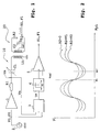
A titre d'exemple, la figure 1 représente le schéma
électrique classique d'un système de détection 10 et d'un
système de modulation de charge 20 coopérant par couplage
inductif.As an example, Figure 1 shows the diagram
electric system with a
Le système 10 comprend une capacité ajustable C1 et
bobine L1 en série formant un circuit résonant. La
capacité C1 est connectée par l'intermédiaire d'une
résistance R1 à la sortie d'un amplificateur
tension/courant 1 recevant en entrée une tension
alternative V0 de fréquence F0, délivrée par un
oscillateur 2. La tension V0, convertie en courant par
l'amplificateur 1, forme le signal d'excitation du
circuit résonant L1C1 dont la fréquence propre Fp1 est
réglée au voisinage de la fréquence d'excitation F0.The
En regard du système de détection 10, le système de
modulation de charge 20 comprend une bobine d'antenne L2
formant avec une capacité C2 un circuit résonnant de
fréquence propre Fp2 accordée à la fréquence F0. La
bobine L2 est connectée en parallèle avec des moyens de
modulation de charge, ici une résistance R2 en série avec
un interrupteur Tm. L'interrupteur Tm est piloté par un
signal S1 de type binaire, de fréquence porteuse F1,
devant être détecté par le système 10. Les modulations de
charge appliquées à la bobine L2 en fonction des
fluctuations du signal S1 se répercutent par couplage
inductif sur la bobine L1, et l'on observe aux bornes du
circuit d'antenne L1C1 une tension alternative Vm de
fréquence F0, modulée en amplitude et en phase.Next to the
Selon une première méthode classique illustrée sur
la figure 1, la détection du signal de modulation de
charge S1 est assurée par un comparateur de phase 3
recevant en entrée les tensions V0 et Vm. Le comparateur
3 délivre une tension Vϕ proportionnelle au déphasage de
ces deux signaux. La tension Vϕ est filtrée par un passe-bande
4 calé sur la fréquence porteuse F1 du signal S1.
La sortie du passe-bande 4 est rendue binaire par un
comparateur 5 à seuil Vref. A la sortie du comparateur 5,
on trouve le signal S1 de fréquence F1.According to a first classic method illustrated on
Figure 1, the detection of the modulation signal
load S1 is provided by a
Cette méthode de détection du signal S1 par
comparaison de phase présente l'avantage d'offrir un bon
rapport signal sur bruit mais nécessite que la fréquence
propre Fp1 du circuit d'antenne L1C1 soit sensiblement
désaccordée vis-à-vis de la fréquence F0. En effet, il
apparaít en pratique que la phase ϕ de la tension Vm
n'est pas sensible aux modulations de charge quand la
fréquence propre Fp1 du circuit d'antenne L1C1 est
rigoureusement égale à la fréquence d'excitation F0. Pour
fixer les idées, on a représenté en figure 2 les courbes
de phase ϕ de la tension Vm en fonction de la fréquence
propre Fp1, pour diverses valeurs 0, v1, v2 de la
résistance de charge R2. Quand Fp1 est égale à F0, on
voit que les courbes de phase se croisent en un même
point et que la sensibilité du système 30 aux modulations
de charge est nulle. En calant la fréquence propre Fp1 du
circuit L1C1 sur un point F0' voisin de F0, on obtient
par contre une bonne sensibilité, la phase ϕ étant
fonction de la charge R2. This method of detecting the signal S1 by
phase comparison has the advantage of offering a good
signal to noise ratio but requires that the frequency
own Fp1 of the antenna circuit L1C1 is substantially
detuned with respect to the frequency F0. Indeed, it
appears in practice that the phase ϕ of the voltage Vm
is not sensitive to load modulations when the
natural frequency Fp1 of the antenna circuit L1C1 is
strictly equal to the excitation frequency F0. For
fix the ideas, we have represented in figure 2 the curves
phase ϕ of voltage Vm as a function of frequency
own Fp1, for
En pratique, cela signifie que la fréquence propre Fp1 du circuit L1C1 doit être ajustée finement par un réglage de la capacité C1, et contrôlée régulièrement pour corriger les dérives de la capacité C1 dues aux conditions climatiques (température, humidité...) et au vieillissement. Cette contrainte rend la méthode impropre à être mise en oeuvre dans un système à maintenance réduite, par exemple un lecteur de carte à puce sans contact disposé dans un lieu public, une station de test automatique de circuits intégrés sans contact,...In practice, this means that the natural frequency Fp1 of circuit L1C1 must be finely adjusted by a capacity adjustment C1, and checked regularly to correct the drifts in capacity C1 due to climatic conditions (temperature, humidity ...) and at aging. This constraint makes the method improper to be implemented in a maintenance system reduced, for example a smart card reader without contact located in a public place, a test station automatic contactless integrated circuits, ...
Pour cette raison, on préfère généralement une seconde méthode classique, consistant à démoduler l'amplitude de la tension Vm aux bornes du circuit résonnant L1C1, pour en extraire le signal S1. Cette seconde méthode présente toutefois l'inconvénient d'offrir un rapport signal sur bruit médiocre.For this reason, we generally prefer a second classic method, consisting in demodulating the amplitude of the voltage Vm across the circuit resonating L1C1, to extract the signal S1 therefrom. This second method has the drawback offer a poor signal-to-noise ratio.
Ainsi, un objectif de la présente invention est de prévoir un système et une méthode de détection de modulation de charge par comparaison de phase qui ne présente pas les inconvénients de la méthode décrite ci-dessus.Thus, an objective of the present invention is to provide a system and a method for detecting load modulation by phase comparison which does not does not have the disadvantages of the method described above.
Selon l'invention cet objectif est atteint par un procédé de détection d'un signal de modulation de charge reçu par couplage inductif dans un circuit d'antenne comportant une bobine de détection excitée par un signal de fréquence prédéterminée, comprenant une étape de comparaison de la phase du signal d'excitation de la bobine avec la phase d'un signal prélevé dans le circuit d'antenne, procédé dans lequel le circuit d'antenne ne forme pas un circuit résonant au voisinage de la fréquence du signal d'excitation, et l'on compare la phase du signal d'excitation avec la phase du courant traversant la bobine de détection.According to the invention this objective is achieved by a method of detecting a load modulation signal received by inductive coupling in an antenna circuit comprising a detection coil excited by a signal of predetermined frequency, comprising a step of comparison of the phase of the excitation signal of the coil with the phase of a signal taken from the circuit antenna, method in which the antenna circuit does not not form a resonant circuit near the frequency of the excitation signal, and the phase of the excitation signal with the phase of the current crossing the detection coil.
Selon un mode de réalisation appliqué à la détection d'un signal de modulation de charge émis par un circuit intégré comportant des moyens pour moduler la charge d'une bobine, la bobine de détection et la bobine du circuit intégré sont respectivement formées par des enroulements primaire et secondaire d'un transformateur, l'enroulement secondaire étant connecté à des plots du circuit intégré.According to an embodiment applied to the detection of a load modulation signal emitted by a integrated circuit comprising means for modulating the load of a coil, the detection coil and the coil of the integrated circuit are respectively formed by primary and secondary windings of a transformer, the secondary winding being connected to the pads of the integrated circuit.
La présente invention concerne également un système de détection par couplage inductif d'un signal de modulation de charge, comprenant un circuit d'antenne comportant une bobine, des moyens pour appliquer au circuit d'antenne un signal d'excitation de fréquence prédéterminée, des moyens comparateurs de phase recevant sur une première entrée le signal d'excitation et sur une deuxième entrée un signal prélevé dans le circuit d'antenne, et des moyens pour extraire le signal de modulation de charge d'un signal de phase délivré par les moyens comparateurs, dans lequel : le circuit d'antenne ne forme pas un circuit résonant au voisinage de la fréquence du signal d'excitation, et les moyens comparateurs de phase reçoivent sur leur deuxième entrée un signal délivré par des moyens de détection du courant traversant la bobine.The present invention also relates to a system detection by inductive coupling of a signal load modulation, including an antenna circuit comprising a coil, means for applying to the antenna circuit a frequency excitation signal predetermined, phase comparator means receiving on a first input the excitation signal and on a second input a signal taken from the circuit antenna, and means for extracting the signal from load modulation of a phase signal delivered by the comparator means, in which: the antenna circuit does not form a resonant circuit near the frequency of the excitation signal, and the means phase comparators receive on their second input a signal delivered by current detection means crossing the coil.
Selon un mode de réalisation, les moyens de détection du courant comprennent un transformateur dont l'enroulement primaire est connecté en série avec la bobine d'antenne.According to one embodiment, the means of current detection include a transformer whose the primary winding is connected in series with the antenna coil.
Selon un mode de réalisation, le secondaire du transformateur est connecté en parallèle avec une résistance, pour convertir en tension le courant traversant le primaire.According to one embodiment, the secondary of transformer is connected in parallel with a resistance, to convert current into voltage crossing the primary.
Selon un mode de réalisation, les moyens pour extraire le signal de modulation de charge comprennent un filtre passe-bande centré sur une fréquence porteuse du signal de modulation de charge. According to one embodiment, the means for extract the load modulation signal include a bandpass filter centered on a carrier frequency of the load modulation signal.
La présente invention concerne également une station de réception de données par couplage inductif et modulation de charge, comprenant un système de détection selon l'invention pour détecter un signal de modulation de charge, et un circuit décodeur pour extraire des données du signal de modulation de charge.The present invention also relates to a data receiving station by inductive coupling and load modulation, including a detection system according to the invention for detecting a modulation signal load, and a decoder circuit for extracting load modulation signal data.
La présente invention concerne également une station de test d'un circuit intégré fonctionnant sans contact au moyen d'une bobine d'antenne, comprenant un système de détection selon l'invention pour détecter un signal de modulation de charge émis par le circuit intégré.The present invention also relates to a integrated circuit test station operating without contact by means of an antenna coil, comprising a detection system according to the invention for detecting a load modulation signal emitted by the circuit integrated.
Selon un mode de réalisation, la bobine du système de détection et la bobine du circuit intégré sont des enroulements primaire et secondaire d'un transformateur.According to one embodiment, the system coil and the coil of the integrated circuit are primary and secondary windings of a transformer.
Selon un mode de réalisation, le station comprend un circuit décodeur pour extraire des données du signal de modulation de charge détecté.According to one embodiment, the station comprises a decoder circuit for extracting data from the signal load modulation detected.
Ces objets, caractéristiques et avantages de la présente invention seront exposés plus en détail dans la description suivante d'un exemple de réalisation d'un système de détection selon l'invention, en relation avec les figures jointes parmi lesquelles :
- la figure 1 précédemment décrite est le schéma électrique d'un système de détection classique d'un signal de modulation de charge,
- la figure 2 précédemment décrite représente, pour plusieurs valeurs de charge, des courbes de phase d'un signal d'antenne en fonction de la fréquence de résonance du circuit d'antenne du système de la figure 1,
- la figure 3 représente le schéma électrique d'un système de détection selon l'invention, et illustre par ailleurs une application de ce système à la réception de données transmises par un circuit intégré fonctionnant sans contact, et
- la figure 4 illustre une application du système de détection de la figure 3 au test de circuits intégrés fonctionnant sans contact, avant la connexion de ces circuits à une bobine d'antenne.
- FIG. 1 previously described is the electrical diagram of a conventional detection system for a charge modulation signal,
- FIG. 2 previously described represents, for several load values, phase curves of an antenna signal as a function of the resonance frequency of the antenna circuit of the system of FIG. 1,
- FIG. 3 represents the electrical diagram of a detection system according to the invention, and also illustrates an application of this system to the reception of data transmitted by an integrated circuit operating without contact, and
- FIG. 4 illustrates an application of the detection system of FIG. 3 to the test of integrated circuits operating without contact, before the connection of these circuits to an antenna coil.
La figure 3 représente, dans sa partie gauche, un
système 30 de détection selon l'invention d'un signal de
modulation de charge. On retrouve dans le système 30 la
plupart des éléments décrits au préambule, dont les
références sont conservées, à l'exception de la capacité
C1 qui est supprimée.Figure 3 shows, in its left part, a
Selon l'invention, le système 30 diffère en effet
de celui de la figure 1 par le fait que le circuit
d'antenne, qui comprend ici uniquement la bobine L1, ne
forme pas un circuit résonant au voisinage de la
fréquence F0 du signal d'excitation V0.According to the invention, the
Par ailleurs, le comparateur de phase 3 délivrant
le signal de phase Vϕ reçoit en entrée le signal
d'excitation V0 et un signal V(Im) qui est l'image du
courant Im traversant la bobine L1. Le signal V(Im) est
délivré par un capteur de courant 31 prenant ici la forme
d'un transformateur ayant des enroulements primaire 31-1
et secondaire 31-2. L'enroulement primaire 31-1 ne
comporte ici qu'une spire et est connecté en série avec
la bobine L1. L'enroulement secondaire 31-2 est connecté
en parallèle avec une résistance Ri de conversion
courant/tension.Furthermore, the
Enfin, le comparateur de phase 3 est réalisé de
façon simple au moyen de deux circuits écrêteurs 3-1, 3-2
dont les sorties attaquent les entrées d'une porte
logique 3-3 du type OU EXCLUSIF, le signal de phase Vϕ
étant délivré par la porte 3-3. Comme précédemment, le
comparateur de phase 3 est connecté à un filtre passe-bande
4 suivi d'un comparateur 5 à seuil Vref.Finally, the
L'avantage du système 30 selon l'invention est
qu'il ne nécessite aucun réglage de son circuit d'antenne
tout en offrant une excellente sensibilité du signal de
phase Vϕ aux modulations de charge. Ce résultat est
obtenu par la combinaison des deux caractéristiques
décrites plus haut, à savoir la prévision d'un circuit
d'antenne non résonnant à la fréquence F0 et aux
fréquences avoisinantes, et une comparaison de phase
basée sur une détection du courant d'antenne Im.The advantage of the
La figure 3 illustre par ailleurs une application
du système 30 à la réception de données émises par un
circuit intégré IC fonctionnant sans contact, dont le
schéma électrique est représenté sur la partie droite de
la figure.Figure 3 also illustrates an application
of the
Le circuit IC est équipé de la bobine d'antenne L2, la capacité C2, la résistance R2 et l'interrupteur de modulation de charge Tm décrits au préambule. Aux bornes de la bobine L2, apparaít une tension induite alternative Vac de fréquence F0, image de la tension Vm présente aux bornes de la bobine L1.The IC circuit is equipped with the antenna coil L2, the capacitor C2, the resistor R2 and the switch load modulation Tm described in the preamble. At the terminals coil L2, appears an alternating induced voltage Vac of frequency F0, image of the voltage Vm present at coil L1 terminals.
Le circuit intégré IC comprend par ailleurs un circuit codeur CD, une mémoire de données MEM, un microprocesseur MP, un circuit diviseur de fréquence DIV et un pont à diodes Pd agencé pour redresser la tension Vac. Le circuit DIV délivre au circuit codeur CD un signal d'horloge extrait de la tension Vac, dont la fréquence F1 est un sous-multiple de la fréquence F0. Le circuit CD, par exemple un codeur BPSK par sauts de phase, reçoit des données numériques DT de la mémoire MEM et délivre le signal S1 de modulation de charge, de fréquence porteuse F1. Enfin, le redresseur Pd délivre une tension continue Vcc assurant l'alimentation électrique du circuit IC.The integrated circuit IC also includes a encoder circuit CD, a data memory MEM, a MP microprocessor, a DIV frequency divider circuit and a Pd diode bridge arranged to rectify the voltage Vac. The DIV circuit delivers to the CD encoder circuit a clock signal extracted from the voltage Vac, the frequency F1 is a sub-multiple of frequency F0. The CD circuit, for example a BPSK encoder by jumps of phase, receives digital data DT from memory MEM and delivers the load modulation signal S1, from carrier frequency F1. Finally, the rectifier Pd delivers a direct voltage Vcc ensuring the supply electrical circuit IC.
Ainsi, les données DT à émettre sont injectées sous
forme codée dans le signal de modulation de charge S1. La
sortie du système 30 est appliquée sur l'entrée d'un
décodeur DEC qui démodule le signal S1 et en extrait les
données numériques DT.Thus, the DT data to be transmitted is injected under
coded form in the load modulation signal S1. The
En pratique, le circuit intégré IC peut être agencé
dans un support portable comme une carte plastique, un
jeton, une étiquette... Le système de détection 30 forme
ainsi, avec le décodeur DEC, une station 50 de réception
de données, par exemple un lecteur de cartes à puce sans
contact. La station 50 peut comprendre des moyens pour
envoyer des données au circuit intégré IC, par exemple
des moyens de modulation de l'amplitude du signal
d'excitation V0. De tels moyens sont bien connus de
l'homme de l'art et ne seront pas décrits ici dans un
souci de simplicité.In practice, the integrated circuit IC can be arranged
in a portable medium such as a plastic card, a
token, a label ... The
A la lecture de ce qui précède, il apparaítra clairement à l'homme de l'art que le système de détection selon l'invention est destiné à fonctionner avec un fort couplage inductif entre les bobines L1 et L2. La présente invention est ainsi réservée à des applications à faible distance de communication, par exemple aux lecteurs de cartes sans contact pourvus d'une fente d'introduction et d'un guide de carte. De tels lecteurs garantissent une faible distance de communication, de l'ordre de quelques millimètres.Upon reading the above, it will appear clearly to those skilled in the art that the detection system according to the invention is intended to operate with a strong inductive coupling between the coils L1 and L2. The current invention is thus reserved for applications with low communication distance, for example to readers of contactless cards with an entry slot and a map guide. Such readers guarantee short communication distance, on the order of a few millimeters.
La présente invention est également applicable à la
réalisation d'une station de test permettant de tester un
circuit intégré sans contact avant son assemblage sur un
support et sa connexion à une bobine d'antenne. Selon un
aspect de la présente invention, on propose de simuler la
bobine d'antenne L2 du circuit intégré au moyen de
l'enroulement secondaire d'un transformateur dont
l'enroulement primaire forme la bobine L1 du système de
détection 30.The present invention is also applicable to the
creation of a test station for testing a
contactless integrated circuit before assembly on a
support and its connection to an antenna coil. According to a
aspect of the present invention, it is proposed to simulate the
antenna coil L2 of the integrated circuit by means of
the secondary winding of a transformer whose
the primary winding forms the coil L1 of the
La figure 4 représente schématiquement une telle
station de test 60. La station 60 comprend un
transformateur TR, le système de détection 30 selon
l'invention, le décodeur DEC déjà décrit et une unité
centrale 61 recevant les données DT délivrées par le
circuit DEC. L'enroulement primaire T1 du transformateur
TR forme la bobine du système de détection 30.
L'enroulement secondaire T2 est relié par l'intermédiaire
de fils électriques 62 à des pointes métalliques 63,64
fixées sur une carte à circuit imprimé 65. Les pointes
63, 64 sont appliquées sur des plots 41, 42 du circuit
intégré IC prévus pour être soudés à une bobine
d'antenne. Ainsi, l'enroulement T2 forme une bobine
d'antenne fictive permettant de faire fonctionner et de
tester le circuit IC avant son montage sur support
portable et sa connexion à une bobine d'antenne.Figure 4 shows schematically such a
Cet aspect de l'invention garantit un fort couplage inductif entre les enroulements T1 et T2 et permet de réaliser une station de test à faible maintenance, ne nécessitant aucun réglage de son circuit d'antenne et pouvant être disposée dans une chaíne de fabrication de circuits intégrés. Les circuits intégrés peuvent être testés alors qu'ils sont encore présents collectivement sur une plaquette mère de silicium, ou "wafer", avant la découpe de la plaquette mère.This aspect of the invention guarantees a strong coupling inductive between the T1 and T2 windings and allows build a low maintenance test station, do not requiring no adjustment of its antenna circuit and can be arranged in a production line of integrated circuits. Integrated circuits can be tested while they are still collectively present on a silicon wafer, or "wafer", before the cutting of the mother wafer.
Il apparaítra clairement à l'homme de l'art que la
présente invention est susceptible de diverses autres
applications et modes de réalisation. Notamment, si l'on
se réfère à nouveau à la figure 3, il est bien évident
que le capteur de courant 31 peut être réalisé de
diverses manières, notamment au moyen d'une résistance de
précision, d'un capteur à effet Hall,...It will be clear to those skilled in the art that the
present invention is susceptible to various other
applications and embodiments. In particular, if we
again refers to Figure 3, it is quite obvious
that the
Claims (10)
Applications Claiming Priority (2)
| Application Number | Priority Date | Filing Date | Title |
|---|---|---|---|
| FR9807678 | 1998-06-18 | ||
| FR9807678A FR2780222B1 (en) | 1998-06-18 | 1998-06-18 | METHOD AND SYSTEM FOR DETECTION BY INDUCTIVE COUPLING OF A LOAD MODULATION SIGNAL |
Publications (2)
| Publication Number | Publication Date |
|---|---|
| EP0966112A1 true EP0966112A1 (en) | 1999-12-22 |
| EP0966112B1 EP0966112B1 (en) | 2001-11-21 |
Family
ID=9527533
Family Applications (1)
| Application Number | Title | Priority Date | Filing Date |
|---|---|---|---|
| EP99111698A Expired - Lifetime EP0966112B1 (en) | 1998-06-18 | 1999-06-17 | Method and system for inductive coupling detection of a charge modulation signal |
Country Status (4)
| Country | Link |
|---|---|
| US (1) | US6329808B1 (en) |
| EP (1) | EP0966112B1 (en) |
| DE (1) | DE69900622T2 (en) |
| FR (1) | FR2780222B1 (en) |
Cited By (1)
| Publication number | Priority date | Publication date | Assignee | Title |
|---|---|---|---|---|
| EP2506185A1 (en) | 2011-03-29 | 2012-10-03 | Pollux | Radiofrequency communication method with detection of the presence of an RFID chip and system implementing such a method. |
Families Citing this family (58)
| Publication number | Priority date | Publication date | Assignee | Title |
|---|---|---|---|---|
| FR2814242B1 (en) * | 2000-09-19 | 2002-12-20 | France Telecom | DEVICE FOR PUNCTUAL MEASUREMENT OF A MAGNETIC FIELD RADIOFREQUENCY OF CONSTANT AMPLITUDE AND FREQUENCY |
| FR2815490B1 (en) * | 2000-10-16 | 2006-07-07 | Inside Technologies | CONTACTLESS INTEGRATED CIRCUIT READER |
| WO2002101952A1 (en) * | 2001-06-12 | 2002-12-19 | Main.Net Communications Ltd. | Coupling circuits for power line communications |
| GB0208449D0 (en) * | 2002-04-10 | 2002-05-22 | Zarlink Semiconductor Ab | Method of saving power in RF devices |
| US7088145B2 (en) * | 2002-12-23 | 2006-08-08 | 3M Innovative Properties Company | AC powered logic circuitry |
| FR2851382B1 (en) * | 2003-02-14 | 2008-07-11 | Baracoda | BLUETOOTH COMMUNICATION MODULE SYSTEM WITH CONTROLLED POWER SUPPLY, RADIOCOMMUNICATION ASSEMBLY, METHODS AND READERS |
| DE10329655A1 (en) * | 2003-07-01 | 2005-02-03 | Infineon Technologies Ag | Electronic component |
| US7078937B2 (en) * | 2003-12-17 | 2006-07-18 | 3M Innovative Properties Company | Logic circuitry powered by partially rectified ac waveform |
| US7508686B2 (en) * | 2005-06-29 | 2009-03-24 | Sigmatel, Inc. | System and method for configuring direct current converter |
| US10693415B2 (en) | 2007-12-05 | 2020-06-23 | Solaredge Technologies Ltd. | Testing of a photovoltaic panel |
| US11881814B2 (en) | 2005-12-05 | 2024-01-23 | Solaredge Technologies Ltd. | Testing of a photovoltaic panel |
| US11309832B2 (en) | 2006-12-06 | 2022-04-19 | Solaredge Technologies Ltd. | Distributed power harvesting systems using DC power sources |
| US8384243B2 (en) | 2007-12-04 | 2013-02-26 | Solaredge Technologies Ltd. | Distributed power harvesting systems using DC power sources |
| US8963369B2 (en) | 2007-12-04 | 2015-02-24 | Solaredge Technologies Ltd. | Distributed power harvesting systems using DC power sources |
| US8473250B2 (en) | 2006-12-06 | 2013-06-25 | Solaredge, Ltd. | Monitoring of distributed power harvesting systems using DC power sources |
| US11569659B2 (en) | 2006-12-06 | 2023-01-31 | Solaredge Technologies Ltd. | Distributed power harvesting systems using DC power sources |
| US8319471B2 (en) | 2006-12-06 | 2012-11-27 | Solaredge, Ltd. | Battery power delivery module |
| US11296650B2 (en) * | 2006-12-06 | 2022-04-05 | Solaredge Technologies Ltd. | System and method for protection during inverter shutdown in distributed power installations |
| US11888387B2 (en) | 2006-12-06 | 2024-01-30 | Solaredge Technologies Ltd. | Safety mechanisms, wake up and shutdown methods in distributed power installations |
| US8947194B2 (en) | 2009-05-26 | 2015-02-03 | Solaredge Technologies Ltd. | Theft detection and prevention in a power generation system |
| US8013472B2 (en) | 2006-12-06 | 2011-09-06 | Solaredge, Ltd. | Method for distributed power harvesting using DC power sources |
| US9088178B2 (en) | 2006-12-06 | 2015-07-21 | Solaredge Technologies Ltd | Distributed power harvesting systems using DC power sources |
| US8319483B2 (en) | 2007-08-06 | 2012-11-27 | Solaredge Technologies Ltd. | Digital average input current control in power converter |
| US11728768B2 (en) | 2006-12-06 | 2023-08-15 | Solaredge Technologies Ltd. | Pairing of components in a direct current distributed power generation system |
| US11855231B2 (en) | 2006-12-06 | 2023-12-26 | Solaredge Technologies Ltd. | Distributed power harvesting systems using DC power sources |
| US11687112B2 (en) | 2006-12-06 | 2023-06-27 | Solaredge Technologies Ltd. | Distributed power harvesting systems using DC power sources |
| US11735910B2 (en) | 2006-12-06 | 2023-08-22 | Solaredge Technologies Ltd. | Distributed power system using direct current power sources |
| US8816535B2 (en) | 2007-10-10 | 2014-08-26 | Solaredge Technologies, Ltd. | System and method for protection during inverter shutdown in distributed power installations |
| US11264947B2 (en) | 2007-12-05 | 2022-03-01 | Solaredge Technologies Ltd. | Testing of a photovoltaic panel |
| JP2011507465A (en) | 2007-12-05 | 2011-03-03 | ソラレッジ テクノロジーズ リミテッド | Safety mechanism, wake-up method and shutdown method in distributed power installation |
| WO2009072076A2 (en) | 2007-12-05 | 2009-06-11 | Solaredge Technologies Ltd. | Current sensing on a mosfet |
| EP3719949A1 (en) | 2008-05-05 | 2020-10-07 | Solaredge Technologies Ltd. | Direct current power combiner |
| CN102804542B (en) * | 2010-01-25 | 2016-09-14 | 捷通国际有限公司 | For detecting the system and method for the data communication through wireless power link |
| GB2508548B (en) * | 2010-01-25 | 2014-08-13 | Access Business Group Int Llc | Systems and methods for detecting data communication over a wireless power link |
| US10230310B2 (en) | 2016-04-05 | 2019-03-12 | Solaredge Technologies Ltd | Safety switch for photovoltaic systems |
| US10673229B2 (en) | 2010-11-09 | 2020-06-02 | Solaredge Technologies Ltd. | Arc detection and prevention in a power generation system |
| US10673222B2 (en) | 2010-11-09 | 2020-06-02 | Solaredge Technologies Ltd. | Arc detection and prevention in a power generation system |
| GB2485527B (en) | 2010-11-09 | 2012-12-19 | Solaredge Technologies Ltd | Arc detection and prevention in a power generation system |
| US9397729B2 (en) | 2010-11-15 | 2016-07-19 | Taiwan Semiconductor Manufacturing Company, Ltd. | Through chip coupling for signal transport |
| JP5750031B2 (en) * | 2010-11-19 | 2015-07-15 | 株式会社半導体エネルギー研究所 | Electronic circuit and semiconductor device |
| TW201236301A (en) | 2010-12-08 | 2012-09-01 | Access Business Group Int Llc | System and method for providing communications in a wireless power supply |
| GB2483317B (en) | 2011-01-12 | 2012-08-22 | Solaredge Technologies Ltd | Serially connected inverters |
| US8731116B2 (en) * | 2011-02-07 | 2014-05-20 | Access Business Group International Llc | System and method of providing communications in a wireless power transfer system |
| KR101218989B1 (en) * | 2011-07-15 | 2013-01-21 | 삼성전기주식회사 | Semiconductor package and manufacturing method thereof |
| US8570005B2 (en) | 2011-09-12 | 2013-10-29 | Solaredge Technologies Ltd. | Direct current link circuit |
| GB2498365A (en) | 2012-01-11 | 2013-07-17 | Solaredge Technologies Ltd | Photovoltaic module |
| GB2498790A (en) | 2012-01-30 | 2013-07-31 | Solaredge Technologies Ltd | Maximising power in a photovoltaic distributed power system |
| GB2498791A (en) | 2012-01-30 | 2013-07-31 | Solaredge Technologies Ltd | Photovoltaic panel circuitry |
| US9853565B2 (en) | 2012-01-30 | 2017-12-26 | Solaredge Technologies Ltd. | Maximized power in a photovoltaic distributed power system |
| GB2499991A (en) | 2012-03-05 | 2013-09-11 | Solaredge Technologies Ltd | DC link circuit for photovoltaic array |
| US9287827B2 (en) * | 2012-09-06 | 2016-03-15 | Qualcomm Incorporated | System and method to demodulate a load modulated signal |
| US9548619B2 (en) | 2013-03-14 | 2017-01-17 | Solaredge Technologies Ltd. | Method and apparatus for storing and depleting energy |
| CN107078558B (en) | 2014-07-30 | 2020-08-04 | 艾尔弗雷德E曼科学研究基金会 | Wireless power transmission and communication |
| CN105429307B (en) * | 2015-11-26 | 2019-02-22 | 南京南瑞集团公司 | Wireless energy signal collection method, wireless sensor awakening method and its device |
| US11018623B2 (en) | 2016-04-05 | 2021-05-25 | Solaredge Technologies Ltd. | Safety switch for photovoltaic systems |
| US11177663B2 (en) | 2016-04-05 | 2021-11-16 | Solaredge Technologies Ltd. | Chain of power devices |
| JP6690609B2 (en) * | 2017-04-06 | 2020-04-28 | 株式会社村田製作所 | Magnetic field generation circuit |
| FR3098908A1 (en) * | 2019-07-19 | 2021-01-22 | Continental Automotive Gmbh | Non-contact sensor for motor vehicle |
Citations (3)
| Publication number | Priority date | Publication date | Assignee | Title |
|---|---|---|---|---|
| US4928087A (en) * | 1988-03-25 | 1990-05-22 | Angewandte Digital Electronik Gmbh | Phase-stabilized, phase-coupled resonant circuit |
| EP0492569A2 (en) * | 1990-12-28 | 1992-07-01 | On Track Innovations Ltd. | A system and method for the non-contact transmission of data |
| EP0704928A2 (en) * | 1994-09-30 | 1996-04-03 | Hughes Identification Devices, Inc. | RF transponder system with parallel resonant interrogation and series resonant response |
Family Cites Families (4)
| Publication number | Priority date | Publication date | Assignee | Title |
|---|---|---|---|---|
| DE3402737C1 (en) * | 1984-01-27 | 1985-08-01 | Angewandte Digital Elektronik Gmbh, 2051 Brunstorf | Mutual information transmission device |
| US4654658A (en) * | 1984-08-03 | 1987-03-31 | Walton Charles A | Identification system with vector phase angle detection |
| US5343079A (en) * | 1991-02-25 | 1994-08-30 | Regents Of The University Of Minnesota | Standby power supply with load-current harmonics neutralizer |
| US5717722A (en) * | 1994-11-08 | 1998-02-10 | Anritsu Corporation | Precision symbol demodulation system for multi-carrier modulation signal |
-
1998
- 1998-06-18 FR FR9807678A patent/FR2780222B1/en not_active Expired - Fee Related
-
1999
- 1999-06-03 US US09/325,188 patent/US6329808B1/en not_active Expired - Lifetime
- 1999-06-17 EP EP99111698A patent/EP0966112B1/en not_active Expired - Lifetime
- 1999-06-17 DE DE69900622T patent/DE69900622T2/en not_active Expired - Lifetime
Patent Citations (3)
| Publication number | Priority date | Publication date | Assignee | Title |
|---|---|---|---|---|
| US4928087A (en) * | 1988-03-25 | 1990-05-22 | Angewandte Digital Electronik Gmbh | Phase-stabilized, phase-coupled resonant circuit |
| EP0492569A2 (en) * | 1990-12-28 | 1992-07-01 | On Track Innovations Ltd. | A system and method for the non-contact transmission of data |
| EP0704928A2 (en) * | 1994-09-30 | 1996-04-03 | Hughes Identification Devices, Inc. | RF transponder system with parallel resonant interrogation and series resonant response |
Cited By (1)
| Publication number | Priority date | Publication date | Assignee | Title |
|---|---|---|---|---|
| EP2506185A1 (en) | 2011-03-29 | 2012-10-03 | Pollux | Radiofrequency communication method with detection of the presence of an RFID chip and system implementing such a method. |
Also Published As
| Publication number | Publication date |
|---|---|
| FR2780222A1 (en) | 1999-12-24 |
| DE69900622D1 (en) | 2002-01-31 |
| DE69900622T2 (en) | 2002-08-01 |
| US6329808B1 (en) | 2001-12-11 |
| EP0966112B1 (en) | 2001-11-21 |
| FR2780222B1 (en) | 2000-08-11 |
Similar Documents
| Publication | Publication Date | Title |
|---|---|---|
| EP0966112B1 (en) | Method and system for inductive coupling detection of a charge modulation signal | |
| US6473028B1 (en) | Detection of the distance between an electromagnetic transponder and a terminal | |
| US6650226B1 (en) | Detection, by an electromagnetic transponder reader, of the distance separating it from a transponder | |
| EP1568130B1 (en) | Tunable antenna circuit, particularly for a wireless integrated circuit reader | |
| EP1312032B1 (en) | High sensitivity reader for passive transponders | |
| CA2318538C (en) | Contact/contactless smart card having customizable antenna interface | |
| EP0898762A1 (en) | Data exchanging system with communication with or without contact between a terminal and portable objects | |
| EP0290547A1 (en) | Identification system. | |
| US6547149B1 (en) | Electromagnetic transponder operating in very close coupling | |
| US6650229B1 (en) | Electromagnetic transponder read terminal operating in very close coupling | |
| US20120161538A1 (en) | Wireless power transmission system | |
| EP0903689A1 (en) | Demodulator for contactless chip card | |
| US6784785B1 (en) | Duplex transmission in an electromagnetic transponder system | |
| KR100411562B1 (en) | Method for ask demodulation and ask demodulator | |
| EP1369813B1 (en) | Reader for electromagnetic transponder | |
| EP0525642B1 (en) | A recording medium reader/writer system and a non-contact IC-card system | |
| EP1043679B1 (en) | Reader having means for determining the distance between the reader and a transponder | |
| US7215723B2 (en) | Demodulator for an amplitude-modulated alternating signal | |
| EP1446765B1 (en) | Receiver circuit and method for a contactless identification system | |
| FR2782209A1 (en) | Inductively-read transponder for access control or payment, switches in capacitor to detune resonant circuit if supply voltage derived from read signal is excessive | |
| JP2005535213A (en) | 2 Repeater with power supply voltage | |
| EP0468848B1 (en) | Electrical connector for chip card and device and method for fraud detection making use of it | |
| JP2006270699A (en) | Non-contact id identifying apparatus | |
| FR2814242A1 (en) | Magnetic receiver for chip cards uses voltage controlled oscillator to convert amplitude to frequency | |
| JP2008502964A (en) | Synchronous phase non-contact demodulation method, related demodulator and reader |
Legal Events
| Date | Code | Title | Description |
|---|---|---|---|
| PUAI | Public reference made under article 153(3) epc to a published international application that has entered the european phase |
Free format text: ORIGINAL CODE: 0009012 |
|
| AK | Designated contracting states |
Kind code of ref document: A1 Designated state(s): AT BE CH CY LI |
|
| AX | Request for extension of the european patent |
Free format text: AL;LT;LV;MK;RO;SI |
|
| 17P | Request for examination filed |
Effective date: 20000504 |
|
| AKX | Designation fees paid |
Free format text: AT BE CH CY LI |
|
| RBV | Designated contracting states (corrected) |
Designated state(s): DE FR GB IT |
|
| REG | Reference to a national code |
Ref country code: DE Ref legal event code: 8566 |
|
| GRAG | Despatch of communication of intention to grant |
Free format text: ORIGINAL CODE: EPIDOS AGRA |
|
| 17Q | First examination report despatched |
Effective date: 20010202 |
|
| GRAG | Despatch of communication of intention to grant |
Free format text: ORIGINAL CODE: EPIDOS AGRA |
|
| GRAH | Despatch of communication of intention to grant a patent |
Free format text: ORIGINAL CODE: EPIDOS IGRA |
|
| GRAG | Despatch of communication of intention to grant |
Free format text: ORIGINAL CODE: EPIDOS AGRA |
|
| GRAH | Despatch of communication of intention to grant a patent |
Free format text: ORIGINAL CODE: EPIDOS IGRA |
|
| GRAH | Despatch of communication of intention to grant a patent |
Free format text: ORIGINAL CODE: EPIDOS IGRA |
|
| GRAA | (expected) grant |
Free format text: ORIGINAL CODE: 0009210 |
|
| AK | Designated contracting states |
Kind code of ref document: B1 Designated state(s): DE FR GB IT |
|
| PG25 | Lapsed in a contracting state [announced via postgrant information from national office to epo] |
Ref country code: IT Free format text: LAPSE BECAUSE OF FAILURE TO SUBMIT A TRANSLATION OF THE DESCRIPTION OR TO PAY THE FEE WITHIN THE PRE;WARNING: LAPSES OF ITALIAN PATENTS WITH EFFECTIVE DATE BEFORE 2007 MAY HAVE OCCURRED AT ANY TIME BEFORE 2007. THE CORRECT EFFECTIVE DATE MAY BE DIFFERENT FROM THE ONE RECORDED.SCRIBED TIME-LIMIT Effective date: 20011121 |
|
| GBT | Gb: translation of ep patent filed (gb section 77(6)(a)/1977) |
Effective date: 20011122 |
|
| RAP2 | Party data changed (patent owner data changed or rights of a patent transferred) |
Owner name: STMICROELECTRONICS S.A. |
|
| REG | Reference to a national code |
Ref country code: GB Ref legal event code: IF02 |
|
| REF | Corresponds to: |
Ref document number: 69900622 Country of ref document: DE Date of ref document: 20020131 |
|
| PLBE | No opposition filed within time limit |
Free format text: ORIGINAL CODE: 0009261 |
|
| STAA | Information on the status of an ep patent application or granted ep patent |
Free format text: STATUS: NO OPPOSITION FILED WITHIN TIME LIMIT |
|
| 26N | No opposition filed | ||
| PGFP | Annual fee paid to national office [announced via postgrant information from national office to epo] |
Ref country code: GB Payment date: 20080527 Year of fee payment: 10 |
|
| GBPC | Gb: european patent ceased through non-payment of renewal fee |
Effective date: 20090617 |
|
| PG25 | Lapsed in a contracting state [announced via postgrant information from national office to epo] |
Ref country code: GB Free format text: LAPSE BECAUSE OF NON-PAYMENT OF DUE FEES Effective date: 20090617 |
|
| PGFP | Annual fee paid to national office [announced via postgrant information from national office to epo] |
Ref country code: FR Payment date: 20100729 Year of fee payment: 12 Ref country code: DE Payment date: 20100610 Year of fee payment: 12 |
|
| REG | Reference to a national code |
Ref country code: FR Ref legal event code: ST Effective date: 20120229 |
|
| REG | Reference to a national code |
Ref country code: DE Ref legal event code: R119 Ref document number: 69900622 Country of ref document: DE Effective date: 20120103 |
|
| PG25 | Lapsed in a contracting state [announced via postgrant information from national office to epo] |
Ref country code: FR Free format text: LAPSE BECAUSE OF NON-PAYMENT OF DUE FEES Effective date: 20110630 Ref country code: DE Free format text: LAPSE BECAUSE OF NON-PAYMENT OF DUE FEES Effective date: 20120103 |