EP0969508A2 - Radiant-energy configurable fuse structure - Google Patents
Radiant-energy configurable fuse structure Download PDFInfo
- Publication number
- EP0969508A2 EP0969508A2 EP99304972A EP99304972A EP0969508A2 EP 0969508 A2 EP0969508 A2 EP 0969508A2 EP 99304972 A EP99304972 A EP 99304972A EP 99304972 A EP99304972 A EP 99304972A EP 0969508 A2 EP0969508 A2 EP 0969508A2
- Authority
- EP
- European Patent Office
- Prior art keywords
- fuse
- energy
- radiant
- fuse body
- configurable
- Prior art date
- Legal status (The legal status is an assumption and is not a legal conclusion. Google has not performed a legal analysis and makes no representation as to the accuracy of the status listed.)
- Withdrawn
Links
- 238000000034 method Methods 0.000 claims description 16
- 239000000758 substrate Substances 0.000 claims description 5
- 238000000151 deposition Methods 0.000 claims description 2
- 238000012856 packing Methods 0.000 abstract description 6
- 238000003491 array Methods 0.000 abstract 1
- 230000008685 targeting Effects 0.000 abstract 1
- 239000012212 insulator Substances 0.000 description 12
- 239000010410 layer Substances 0.000 description 12
- 239000000463 material Substances 0.000 description 10
- 238000007664 blowing Methods 0.000 description 6
- 230000008569 process Effects 0.000 description 6
- 230000009467 reduction Effects 0.000 description 4
- VYPSYNLAJGMNEJ-UHFFFAOYSA-N Silicium dioxide Chemical compound O=[Si]=O VYPSYNLAJGMNEJ-UHFFFAOYSA-N 0.000 description 3
- 230000003667 anti-reflective effect Effects 0.000 description 3
- 230000008901 benefit Effects 0.000 description 3
- 239000004020 conductor Substances 0.000 description 3
- 239000007788 liquid Substances 0.000 description 3
- 229910052814 silicon oxide Inorganic materials 0.000 description 3
- 229910052581 Si3N4 Inorganic materials 0.000 description 2
- NRTOMJZYCJJWKI-UHFFFAOYSA-N Titanium nitride Chemical compound [Ti]#N NRTOMJZYCJJWKI-UHFFFAOYSA-N 0.000 description 2
- 229910052782 aluminium Inorganic materials 0.000 description 2
- XAGFODPZIPBFFR-UHFFFAOYSA-N aluminium Chemical compound [Al] XAGFODPZIPBFFR-UHFFFAOYSA-N 0.000 description 2
- 230000005540 biological transmission Effects 0.000 description 2
- 239000005380 borophosphosilicate glass Substances 0.000 description 2
- 150000001875 compounds Chemical class 0.000 description 2
- 230000003247 decreasing effect Effects 0.000 description 2
- 230000000694 effects Effects 0.000 description 2
- 229910052751 metal Inorganic materials 0.000 description 2
- 239000002184 metal Substances 0.000 description 2
- 238000012986 modification Methods 0.000 description 2
- 230000004048 modification Effects 0.000 description 2
- 230000000717 retained effect Effects 0.000 description 2
- 239000004065 semiconductor Substances 0.000 description 2
- 229910021332 silicide Inorganic materials 0.000 description 2
- HQVNEWCFYHHQES-UHFFFAOYSA-N silicon nitride Chemical compound N12[Si]34N5[Si]62N3[Si]51N64 HQVNEWCFYHHQES-UHFFFAOYSA-N 0.000 description 2
- 239000010936 titanium Substances 0.000 description 2
- MAKDTFFYCIMFQP-UHFFFAOYSA-N titanium tungsten Chemical compound [Ti].[W] MAKDTFFYCIMFQP-UHFFFAOYSA-N 0.000 description 2
- -1 AlSi or AlSiCu Chemical compound 0.000 description 1
- 229910000789 Aluminium-silicon alloy Inorganic materials 0.000 description 1
- RTAQQCXQSZGOHL-UHFFFAOYSA-N Titanium Chemical compound [Ti] RTAQQCXQSZGOHL-UHFFFAOYSA-N 0.000 description 1
- 239000003990 capacitor Substances 0.000 description 1
- 230000008859 change Effects 0.000 description 1
- 230000008021 deposition Effects 0.000 description 1
- 239000003989 dielectric material Substances 0.000 description 1
- 238000004880 explosion Methods 0.000 description 1
- 238000009413 insulation Methods 0.000 description 1
- 238000002955 isolation Methods 0.000 description 1
- 238000004519 manufacturing process Methods 0.000 description 1
- 150000002739 metals Chemical class 0.000 description 1
- 229910021420 polycrystalline silicon Inorganic materials 0.000 description 1
- 229920005591 polysilicon Polymers 0.000 description 1
- 230000008439 repair process Effects 0.000 description 1
- 239000002356 single layer Substances 0.000 description 1
- 239000007787 solid Substances 0.000 description 1
- 229910052719 titanium Inorganic materials 0.000 description 1
- WFKWXMTUELFFGS-UHFFFAOYSA-N tungsten Chemical compound [W] WFKWXMTUELFFGS-UHFFFAOYSA-N 0.000 description 1
- 229910052721 tungsten Inorganic materials 0.000 description 1
- 239000010937 tungsten Substances 0.000 description 1
- 230000008016 vaporization Effects 0.000 description 1
- 238000009834 vaporization Methods 0.000 description 1
Images


Classifications
-
- H—ELECTRICITY
- H01—ELECTRIC ELEMENTS
- H01L—SEMICONDUCTOR DEVICES NOT COVERED BY CLASS H10
- H01L23/00—Details of semiconductor or other solid state devices
- H01L23/52—Arrangements for conducting electric current within the device in operation from one component to another, i.e. interconnections, e.g. wires, lead frames
- H01L23/522—Arrangements for conducting electric current within the device in operation from one component to another, i.e. interconnections, e.g. wires, lead frames including external interconnections consisting of a multilayer structure of conductive and insulating layers inseparably formed on the semiconductor body
- H01L23/525—Arrangements for conducting electric current within the device in operation from one component to another, i.e. interconnections, e.g. wires, lead frames including external interconnections consisting of a multilayer structure of conductive and insulating layers inseparably formed on the semiconductor body with adaptable interconnections
- H01L23/5256—Arrangements for conducting electric current within the device in operation from one component to another, i.e. interconnections, e.g. wires, lead frames including external interconnections consisting of a multilayer structure of conductive and insulating layers inseparably formed on the semiconductor body with adaptable interconnections comprising fuses, i.e. connections having their state changed from conductive to non-conductive
- H01L23/5258—Arrangements for conducting electric current within the device in operation from one component to another, i.e. interconnections, e.g. wires, lead frames including external interconnections consisting of a multilayer structure of conductive and insulating layers inseparably formed on the semiconductor body with adaptable interconnections comprising fuses, i.e. connections having their state changed from conductive to non-conductive the change of state resulting from the use of an external beam, e.g. laser beam or ion beam
-
- H—ELECTRICITY
- H01—ELECTRIC ELEMENTS
- H01L—SEMICONDUCTOR DEVICES NOT COVERED BY CLASS H10
- H01L2924/00—Indexing scheme for arrangements or methods for connecting or disconnecting semiconductor or solid-state bodies as covered by H01L24/00
- H01L2924/0001—Technical content checked by a classifier
- H01L2924/0002—Not covered by any one of groups H01L24/00, H01L24/00 and H01L2224/00
Landscapes
- Physics & Mathematics (AREA)
- Condensed Matter Physics & Semiconductors (AREA)
- General Physics & Mathematics (AREA)
- Engineering & Computer Science (AREA)
- Computer Hardware Design (AREA)
- Microelectronics & Electronic Packaging (AREA)
- Power Engineering (AREA)
- Fuses (AREA)
- Design And Manufacture Of Integrated Circuits (AREA)
Abstract
Description
- The present invention relates generally to radiant-energy fuse structures which are configured to customize electronic devices.
- Configurable fuses are widely used in the electronics industry for the configuration or repair of elements in memory and logic circuits. These fuses are made from conductive materials such as polysilicon, silicides, and metals. The fuses are typically formed on and covered by one or more insulating layers such as silicon oxide or silicon nitride, thus encapsulating the fuse. During configuration, selected fuses are typically irradiated from above by a radiant energy beam, which is generally circular or elliptical in shape and provides a measurable radiant energy. The most common means of providing this energy is through a laser beam, such as the Model 1225hp manufactured by Electro-Scientific Incorporated (ESI) of Portland, Oregon. The radiant energy heats the material in the fuse until a portion of it becomes a liquid, a vapor, or a combination thereof (hereinafter referred to as a liquid/vapor state). Simultaneously, heat propagates along the length of the fuse from the irradiated to the non-irradiated sections. The change in the fuse material state from a solid to a liquid/vapor state causes pressure to build up in the cavity that contains the fuse. This results in a rupturing of the insulator, typically along the structurally-weakest point. At least a portion of the fuse material escapes through this ruptured area. The thickness of the insulator over the fuse is usually chosen to be thinner than the film surrounding the fuse so that the insulator portion over the fuse will be the first area to undergo structural failure when the pressure reaches a critical value. In this manner, the insulator over the fuse will be blown off and the force of the explosion directed away from neighboring critical circuit elements. It is common for the thickness of the insulator to be set to a value that provides the most consistent results in disconnection of the fuse (hereafter generally referred to as fuse blowing).
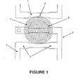
- Figure 1 illustrates a top plan view of a conventional electronic device having conventional
configurable fuses 1. Each offuses 1 has afuse body 2, which is typically the same width or narrower thanconnection terminals 3 connectingconductive lines radiant energy beam 7 severs the connection betweenline 4 andline 5 by directing the beam atfuse body 2. Because the thermal conductivity of the fuse material greatly exceeds that of a typical insulator which encloses the fuse, the majority of the transmitted heat from theradiant energy beam 7 is conducted through theconnection terminals 3, and not the insulator. Thus, theconnection terminals 3 must be long enough to protectlines lines beam 7 typically has a radial energy distribution which is approximately Gaussian in nature, increasing the beam energy necessarily increases theeffective spot size 6 of beam 7 (effective spot size being defined as the diameter of the area of radiant energy beam which could affect active circuit elements). Thus, as the energy increases, adjacent ones offuses 1 must be spaced further apart. Consequently, the packing density of theconventional fuses 1 is relatively low, requiring significant layout area when compared with simple non-configurable interconnect lines. The result is an undesirable lower density and larger size device. - With a conventional fuse design as shown in Figure 1, some of the energy is captured along the length of the
fuse body 2, while much of the remainder is lost outside the much narrower fuse body width. The energy not captured by thefuse body 2 is then free to travel past the fuse to any underlying circuit elements which might be routed below it. Therefore, it has been common for the area around and under the fuses to be clear of circuit elements (e.g., transistors, resistors, signal lines, junctions, etc.) so that the radiant energy used to configure the fuses does not damage these circuit elements. The addition of this clear area increases the overall size of the device, as does the additional area required to place or route circuit elements away from the fuse area. - The conventional fuse design is also subject to inconsistency in fuse blowing. Variations in the thickness of the fuse material and the insulator over the fuse can result in the fuse blowing earlier or later in the fuse blowing process and producing irregularly sized and shaped holes from which the fuse material escapes. Thus, the fuse material may not be sufficiently vaporized to complete the disconnection, or the surrounding insulator may rupture, thereby damaging neighboring circuit elements.
- The above manufacturing constraints seriously complicate how an electronic device can be laid out and effectively increases the area for the circuit elements of the device.
- The present invention seeks to provide a radiant-energy fuse structure having advantages over known fuse structures.
- The present invention provides a radiant-energy configurable fuse having a fuse body wider than at least one of the fuse connection terminals.
- More specifically, in one embodiment of the invention, a fuse comprises a fuse body extending outwardly to two fuse terminals. The fuse body is defined as the area generally irradiated by the radiant energy beam, while the terminals are defined as the areas which connect the fuse body to surrounding circuitry. The fuse body has a larger width than at least one of the two fuse terminals.
- In accordance with another aspect of this invention, a method is provided which allows an electronic device to be formed with circuit elements underlying radiant-energy configurable fuses. The method includes providing a substrate having circuit elements, forming an insulation layer above the circuit elements, and forming at least one configurable fuse having a fuse body and two fuse terminals, whereby the width of the fuse body is greater than the width of at least one of the two connection terminals.
- The fuse body structure of the present invention allows a greater capture of the energy delivered by the radiant-energy beam over the conventional fuse design, thereby permitting the overall delivered energy to be reduced. This will in turn reduce the effective spot size. Since the effective spot size is smaller, the fuses can be placed closer together without risking damage to a neighboring fuse. The lower energy will in some cases also permit the presence of circuit elements below the fuse locations. Either benefit will result in a desirable reduction in the size of the electronic device. The geometry of the fuse body structure also allows a more consistent decapping of the insulator over the fuse during the configuration process, which results in more complete vaporization of the fuse material, leading to a more reliable configuration of the fuse. The lower energy minimizes the risk of rupturing the insulator towards a neighboring circuit element, also leading to a more reliable configuration of the fuse.
- The connection terminals of the present invention are preferably the minimum allowed line width for the patterned interconnect layer in which the fuse resides. This narrow width provides the maximum resistance to undesired heat conduction from the fuse body through the connection terminals to adjacent circuit elements. This feature results in a more restrictive path for the heat to conduct away from the fuse body, thereby reducing the need to have relatively long connection terminals to provide thermal isolation. Thus, the terminal length can be shortened, resulting in a shorter overall fuse length and increasing packing density. The reduction in heat loss also results in more energy being retained by the fuse body for the fuse disconnection process.
- The present invention will be better understood in light of the following detailed description taken together with the accompanying drawings.
- Figure 1 illustrates a top plan view of a portion of an electronic device having conventional fuses;
- Figure 2A illustrates a top plan view of a portion of an electronic device with radiant-energy configurable fuses in accordance with one embodiment of the present invention;
- Figure 2B illustrates the top plan view of a portion of an electronic device with radiant-energy configurable fuses in accordance with another embodiment of the present invention;
- Figure 3A illustrates a top plan view of a portion of an electronic device with the radiant-energy configurable fuses of Figure 2A overlying circuit elements; and
- Figure 3B illustrates a front cross-sectional view along sectional lines 1-1 of the embodiment of Figure 3A.
- Use of the same reference numbers in different figures indicates similar or like elements.
-
- There are several factors which are considered when evaluating an effective fuse design. The area of the fuse body will determine how much of the applied laser energy is captured by the fuse and used in the fuse blowing process, and also how much energy misses the fuse and is available to disrupt underlying or neighboring circuit elements. A larger fuse area will result in a greater capture of this energy. Moreover, for any given thickness of the oxide or dielectric over the fuse, a larger fuse area will reduce the amount of energy required to break the oxide and complete this disconnection. Thus, increasing the fuse width in a conventional fuse design results in more desirable results for these factors. However, a wider fuse results in a larger transmission path for the thermal energy to escape and damage neighboring circuitry, and also results in less of the applied energy being available for the fuse blowing process. This can be compensated for by increasing the length of the fuse terminals so that the heat conduction does not reach neighboring circuitry, but this results in an undesirable reduction in the packing density of the fuses, and a larger overall circuit design. Narrowing the fuse width in a conventional design reduces the undesired thermal transmission, but has the negative effect of reducing the area of the fuse, thus lowering the amount of energy captured, increasing the energy required to break the overlying oxide, and increasing the amount of energy that misses the fuse and can damage underlying circuitry. Thus, one variable in the design cannot be changed without having a negative effect on the other. The design of the present invention allows the variable of fuse area, shape, and terminal width to be independently adjusted to optimum values.
- Figure 2A illustrates a portion of an electronic device with radiant-energy configurable fuses 10 in accordance with one embodiment of the present invention. Depending on the desired characteristic properties, the configurable fuses 10 can be made from conductive materials including aluminum (Al), compounds of aluminum such as AlSi or AlSiCu, tungsten (W), titanium (Ti) or its commonly used compounds such as titanium-tungsten (TiW) or titanium-nitride (TiN), silicides commonly used in the industry, or any other conductive material capable of forming radiant-energy configurable fuses.
- For applications where the fuse body is composed of metal, the
fuses 10 may also have an anti-reflective layer (not shown) formed on the top surface to better enable the fuses to absorb the radiant-energy used for configuration. Titanium-nitride and titanium-tungsten are two such commonly used materials with anti-reflective properties which can be formed on thefuses 10 by conventional and well known methods. - Each of
fuses 10 has afuse body 11 wider than at least one ofconnection terminals 12, which electrically connect adjacentconductive lines radiant energy beam 16 directs a beam with aspot size 15 larger than thefuse body 11 to blow the fuse and sever the electrical connection. The energy distribution of theradiant energy beam 16 is known to approximate a radial Gaussian distribution. To increase the ratio of captured radiant energy to fuse area above that of conventional fuse designs, the shape offuse body 11 is circular and wider than thefuse terminals 12, which allowsfuse body 11 to capture a maximum amount of the energy applied by theradiant energy beam 16. Accordingly, the shape offuse body 11 should be generally circular or elliptical because a circle maximizes the surface area-to-perimeter ratio. However, in practical applications, such a fuse is implemented with a polygonal-shaped fuse body, as shown in Figure 2A. The polygonal shape can be approximately circular, as shown in Figure 2A, or approximately ovate, as show in Figure 2B. - Since the captured energy increases, the amount of applied energy which is necessary to blow the fuse can be reduced, thus reducing the
effective spot size 15. Theconnection terminals 12 are narrowed to the minimum allowed linewidth. This presents a smaller outlet for thermal conduction, thereby reducing the amount of thermal energy transferred away from thefuse body 11. This reduction has two desirable consequences. First, more heat is retained by thefuse body 11, further decreasing the amount of applied energy required to blow the fuse by theradiant energy beam 16 and reducing theeffective spot size 15. Second, the length of thefuse terminals 12 can be shortened since the requirement to isolate heat fromlines fuses 10 and decrease the overall size of the electronic device. - The circular shape of the fuse body has additional benefits. By maximizing the ratio of the surface area to the perimeter of the
fuse body 11, the energy and pressure required to blow a fuse are minimized. As will be apparent to one skilled in the art, the shape of thefuse body 11 does not have to be perfectly circular, but could be ovate or polygonal to improve this ratio while optimizing the shape for a particular combination of fuse materials and insulator thickness over the fuse. - Figure 3A is a top view of the fuse structure of Figure 2A overlying conductive interconnect lines 17. Figure 3B is a side view along sectional line 1-1 of Figure 3A, and illustrates an embodiment of the present invention wherein the energy required to blow the fuse is low enough that circuit elements can be placed underneath the fuses. The electronic device includes
interconnect lines 17 formed above asemiconductor substrate 18 of either an N-type or a P-type conductivity. Because the present invention relates to the effective configuration and protection of circuit elements, theinterconnect lines 17 have been provided for simplicity only. It should be recognized by persons who are skilled in the art that theinterconnect lines 17 could represent various types of circuit elements. For example, circuit elements or active circuitry such as transistors, diodes, resistors, capacitors, or even a P/N-well in an N/P-type semiconductor substrate could be used instead of the interconnect lines 17. - Between the
interconnect lines 17 and afuse layer 9 containingfuses 10, an insulatinglayer 19 is formed using conventional and well known methods. The insulatinglayer 19 can include one or more layers made from one or more different dielectric materials such as silicon oxide and boro-phosphosilicate glass (BPSG). As in other embodiments, thefuse layer 9 may be a single or multiple layer structure formed with conventional and well known methods of deposition, and may also include an anti-reflective layer (not shown) to better enable thefuse body 11 to absorb the radiant energy used for configuration. The fuses 10 formed on insulatinglayer 19 are encapsulated with a second insulatinglayer 20, such as silicon oxide or silicon nitride.Radiant energy beam 16 has a non-uniform intensity, with the intensity decreasing along a radius from the center of the beam. The majority of the energy delivered is absorbed or reflected byfuse body 11, thus protecting theunderlying interconnect lines 17 from damage. Because the design offuse body 11 is optimized to capture the majority of the energy delivered by theradiant energy beam 16 and minimize the loss of this energy through thermal conduction, a relatively low level of radiant energy can be used to configure the fuse. This in turn minimizes the amount of energy which impacts theinterconnect lines 17, further reducing the risk of damage. - Therefore, the fuse structure in accordance with the present invention provides several desirable features, including an increased laser fuse yield at a given laser energy, a larger process window for laser energy without substrate damage and with sufficient reliability of the fuse disconnection, a reduced area required for a fuse, thus increasing packing density and reducing overall circuit size, and an ability to place active circuit elements below the fuses, thus making more efficient use of the area around and under the fuses and further reducing the overall circuit size.
- The above-described embodiments of the present invention are merely meant to be illustrative and not limiting. It will thus be obvious to those skilled in the art that various changes and modifications may be made without departing from this invention in its broader aspects. Therefore, the appended claims encompass all such changes and modifications as fall within the true spirit and scope of this invention.
Claims (16)
- A fuse structure (10) for customizing or repairing an electrical device, the structure comprising:a radiant-energy configurable fuse body (11) located between two conductive elements (13, 14);a first terminal (12) connecting said fuse body (11) to one (13) of said conductive elements; anda second terminal (12) connecting said fuse body (11) to the other (14) of said conductive elements, characterized in that said fuse body (11) is wider than at least one of said first and second terminals (12).
- A structure as claimed in Claim 1, wherein said radiant-energy configurable fuse body (11) is wider than said first and second terminals (12).
- A structure as claimed in Claim 1 or 2, wherein said radiant-energy configurable fuse body (11) is polygonal, having five or more sides.
- A structure as claimed in any one of Claims 1-3, wherein said radiant-energy configurable fuse body (11) is polygonal and approximately circular.
- A structure as claimed in any one of Claims 1-3, wherein said radiant-energy configurable fuse body (11) is polygonal and approximately ovate.
- A structure as claimed in Claim 1 or 2, wherein said radiant-energy configurable fuse body (11) is circular.
- A structure as claimed in Claim 1 or 2, wherein said radiant-energy configurable fuse body (11) is ovate.
- A structure as claimed in any one of Claims 1 to 7, wherein said first and second terminals (12) are approximately co-planar with said radiant-energy configurable fuse body (11).
- A structure as claimed in any one of Claims 1 to 8, wherein said radiant-energy configurable fuse body is at least 50% wider than at least one of said first and second terminals.
- A structure as claimed in any one of Claims 1 to 9, wherein said radiant-energy configurable fuse body (11) is arranged to be electrically disconnected from said two conductive elements (13, 14) by exposure to an energy beam.
- A radiant-energy configurable array having a fuse layer (9, 11) comprising a fuse structure as claimed in any one of Claims 1 to 10 the array including the two conductive elements (13, 14) of Claim 1, and also including an electrically conductive circuit element layer (17) underlying said fuse layer (9, 11) and an insulating layer (19) located between said fuse layer (9, 11) and said electrically conductive circuit element layer (17).
- The array as claimed in Claim 11, wherein said insulating layer (19) is located below said fuse layer (9, 11).
- The array as claimed in Claim 11 or 12, wherein said circuit elements (17) are comprised of circuit elements positioned below said radiant-energy configurable fuse body (11).
- A method of forming a radiant-energy configurable array, said method comprising:forming a fuse layer (9, 11) on an insulating layer (19);forming at least one radiant-energy beam configurable fuse body (11) ;forming circuit elements (13, 14); andforming terminals (12) connecting said at least one fuse body (11) to said circuit elements (13, 14), wherein said at least one fuse body (11) is wider than said terminals (12).
- A method of forming a radiant-energy configurable array, said method comprising:forming a first set of electrically conductive circuit elements (17) over a substrate;depositing an insulating layer (19) on said first set of circuit elements (17);forming a fuse layer (9, 11) on said insulating layer;forming at least one radiant-energy beam configurable fuse body (11) over said first set of circuit elements (17);forming a second set of circuit elements (13, 14); andforming terminals (12) connecting said at least one fuse body (11) to said second set of circuit elements (13, 14) wherein said at least one fuse body (11) is wider than said terminals (12).
- The method of Claim 16, further comprising exposing a selected one of said at least one radiant-energy configurable fuse body (11) with an energy beam for electrically disconnecting said selected radiant-energy configurable fuse (11) from said conductive elements (13, 14).
Applications Claiming Priority (2)
| Application Number | Priority Date | Filing Date | Title |
|---|---|---|---|
| US107841 | 1998-06-30 | ||
| US09/107,841 US5949323A (en) | 1998-06-30 | 1998-06-30 | Non-uniform width configurable fuse structure |
Publications (2)
| Publication Number | Publication Date |
|---|---|
| EP0969508A2 true EP0969508A2 (en) | 2000-01-05 |
| EP0969508A3 EP0969508A3 (en) | 2003-03-05 |
Family
ID=22318762
Family Applications (1)
| Application Number | Title | Priority Date | Filing Date |
|---|---|---|---|
| EP99304972A Withdrawn EP0969508A3 (en) | 1998-06-30 | 1999-06-24 | Radiant-energy configurable fuse structure |
Country Status (3)
| Country | Link |
|---|---|
| US (1) | US5949323A (en) |
| EP (1) | EP0969508A3 (en) |
| JP (1) | JP2000030587A (en) |
Families Citing this family (32)
| Publication number | Priority date | Publication date | Assignee | Title |
|---|---|---|---|---|
| JP4390297B2 (en) * | 1998-06-19 | 2009-12-24 | 株式会社ルネサステクノロジ | Semiconductor device |
| JP3630999B2 (en) | 1998-08-19 | 2005-03-23 | 富士通株式会社 | Semiconductor device and manufacturing method thereof |
| US6380838B1 (en) * | 1999-06-07 | 2002-04-30 | Nec Corporation | Semiconductor device with repair fuses and laser trimming method used therefor |
| US6486527B1 (en) * | 1999-06-25 | 2002-11-26 | Macpherson John | Vertical fuse structure for integrated circuits containing an exposure window in the layer over the fuse structure to facilitate programming thereafter |
| US6225652B1 (en) * | 1999-08-02 | 2001-05-01 | Clear Logic, Inc. | Vertical laser fuse structure allowing increased packing density |
| US6355968B1 (en) * | 2000-08-10 | 2002-03-12 | Infineon Technologies Ag | Wiring through terminal via fuse |
| US6566730B1 (en) | 2000-11-27 | 2003-05-20 | Lsi Logic Corporation | Laser-breakable fuse link with alignment and break point promotion structures |
| JP4079600B2 (en) * | 2001-03-06 | 2008-04-23 | 株式会社東芝 | Semiconductor device |
| DE10112543A1 (en) * | 2001-03-15 | 2002-10-02 | Infineon Technologies Ag | Integrated circuit with electrical connection elements |
| EP1396003A1 (en) * | 2001-06-11 | 2004-03-10 | Wickmann-Werke GmbH | Fuse component |
| JP4225708B2 (en) * | 2001-06-12 | 2009-02-18 | 株式会社東芝 | Semiconductor device |
| JP3445585B2 (en) * | 2001-08-31 | 2003-09-08 | 沖電気工業株式会社 | Method for manufacturing semiconductor device |
| US20040004268A1 (en) * | 2002-07-08 | 2004-01-08 | International Business Machines Corporation | E-Fuse and anti-E-Fuse device structures and methods |
| TW540151B (en) * | 2002-07-19 | 2003-07-01 | Nanya Technology Corp | Fuse structure |
| JP2005039220A (en) * | 2003-06-26 | 2005-02-10 | Nec Electronics Corp | Semiconductor device |
| US6960978B2 (en) * | 2003-07-16 | 2005-11-01 | Hewlett-Packard Development Company, L.P. | Fuse structure |
| US7629234B2 (en) * | 2004-06-18 | 2009-12-08 | Electro Scientific Industries, Inc. | Semiconductor structure processing using multiple laterally spaced laser beam spots with joint velocity profiling |
| JP4685388B2 (en) * | 2004-09-06 | 2011-05-18 | Okiセミコンダクタ株式会社 | Semiconductor device |
| JP4741907B2 (en) * | 2005-09-05 | 2011-08-10 | ルネサスエレクトロニクス株式会社 | Semiconductor device and manufacturing method thereof |
| US20090009281A1 (en) * | 2007-07-06 | 2009-01-08 | Cyntec Company | Fuse element and manufacturing method thereof |
| US20090040006A1 (en) * | 2007-08-08 | 2009-02-12 | International Business Machines Corporation | Electrical fuse with enhanced programming current divergence |
| JP2009170903A (en) * | 2008-01-16 | 2009-07-30 | Hynix Semiconductor Inc | Fuse having cutting regions and fuse set structure having same |
| KR20090090161A (en) * | 2008-02-20 | 2009-08-25 | 삼성전자주식회사 | Electrical fuse device |
| JP5307437B2 (en) * | 2008-04-14 | 2013-10-02 | ルネサスエレクトロニクス株式会社 | Semiconductor device |
| KR20090112390A (en) * | 2008-04-24 | 2009-10-28 | 삼성전자주식회사 | Electrical fuse device |
| KR101043841B1 (en) * | 2008-10-14 | 2011-06-22 | 주식회사 하이닉스반도체 | Fuse in semiconductor |
| KR101046229B1 (en) * | 2009-03-17 | 2011-07-04 | 주식회사 하이닉스반도체 | Semiconductor device including a fuse |
| JP2015144222A (en) * | 2014-01-31 | 2015-08-06 | セイコーインスツル株式会社 | semiconductor device |
| JP2018170455A (en) | 2017-03-30 | 2018-11-01 | エイブリック株式会社 | Semiconductor device |
| CN109244040B (en) * | 2018-07-23 | 2021-08-20 | 珠海市杰理科技股份有限公司 | Chip fuse structure and chip |
| US10833007B2 (en) | 2019-01-08 | 2020-11-10 | International Business Machines Corporation | Circular ring shape fuse device |
| JP7433811B2 (en) * | 2019-08-23 | 2024-02-20 | デクセリアルズ株式会社 | Fuse elements, fuse elements and protection elements |
Citations (5)
| Publication number | Priority date | Publication date | Assignee | Title |
|---|---|---|---|---|
| JPS6057951A (en) * | 1983-09-09 | 1985-04-03 | Mitsubishi Electric Corp | Semiconductor device |
| JPH06104338A (en) * | 1992-09-21 | 1994-04-15 | Kawasaki Steel Corp | Fuse element for repairing memory cell |
| JPH06244285A (en) * | 1993-02-15 | 1994-09-02 | Matsushita Electron Corp | Semiconductor device |
| JPH09213804A (en) * | 1996-01-29 | 1997-08-15 | Mitsubishi Electric Corp | Semiconductor device with fuse layer |
| JPH10163331A (en) * | 1996-12-03 | 1998-06-19 | Texas Instr Japan Ltd | Fuse for semiconductor device and semiconductor device |
Family Cites Families (9)
| Publication number | Priority date | Publication date | Assignee | Title |
|---|---|---|---|---|
| US4814853A (en) * | 1981-10-28 | 1989-03-21 | Tokyo Shibaura Denki Kabushiki Kaisha | Semiconductor device with programmable fuse |
| US4417224A (en) * | 1981-12-16 | 1983-11-22 | Federal Pacific Electric Co. | Time delay fuse |
| US4910418A (en) * | 1988-12-29 | 1990-03-20 | Gazelle Microcircuits, Inc. | Semiconductor fuse programmable array structure |
| US4973932A (en) * | 1989-12-08 | 1990-11-27 | Littelfuse, Inc. | Electrical fuse with coated time delay element |
| US5120152A (en) * | 1990-06-25 | 1992-06-09 | Carmen Gueli | Fusible link |
| US5084691A (en) * | 1990-10-01 | 1992-01-28 | Motorola, Inc. | Controllable fuse |
| US5451811A (en) * | 1991-10-08 | 1995-09-19 | Aptix Corporation | Electrically programmable interconnect element for integrated circuits |
| JP3272028B2 (en) * | 1992-05-13 | 2002-04-08 | 株式会社東芝 | Electronic circuit |
| US5420455A (en) * | 1994-03-31 | 1995-05-30 | International Business Machines Corp. | Array fuse damage protection devices and fabrication method |
-
1998
- 1998-06-30 US US09/107,841 patent/US5949323A/en not_active Expired - Fee Related
-
1999
- 1999-06-24 EP EP99304972A patent/EP0969508A3/en not_active Withdrawn
- 1999-06-28 JP JP11181136A patent/JP2000030587A/en active Pending
Patent Citations (5)
| Publication number | Priority date | Publication date | Assignee | Title |
|---|---|---|---|---|
| JPS6057951A (en) * | 1983-09-09 | 1985-04-03 | Mitsubishi Electric Corp | Semiconductor device |
| JPH06104338A (en) * | 1992-09-21 | 1994-04-15 | Kawasaki Steel Corp | Fuse element for repairing memory cell |
| JPH06244285A (en) * | 1993-02-15 | 1994-09-02 | Matsushita Electron Corp | Semiconductor device |
| JPH09213804A (en) * | 1996-01-29 | 1997-08-15 | Mitsubishi Electric Corp | Semiconductor device with fuse layer |
| JPH10163331A (en) * | 1996-12-03 | 1998-06-19 | Texas Instr Japan Ltd | Fuse for semiconductor device and semiconductor device |
Non-Patent Citations (5)
| Title |
|---|
| PATENT ABSTRACTS OF JAPAN vol. 009, no. 189 (E-333), 6 August 1985 (1985-08-06) -& JP 60 057951 A (MITSUBISHI DENKI KK), 3 April 1985 (1985-04-03) * |
| PATENT ABSTRACTS OF JAPAN vol. 018, no. 372 (E-1577), 13 July 1994 (1994-07-13) -& JP 06 104338 A (KAWASAKI STEEL CORP), 15 April 1994 (1994-04-15) * |
| PATENT ABSTRACTS OF JAPAN vol. 018, no. 626 (E-1636), 29 November 1994 (1994-11-29) -& JP 06 244285 A (MATSUSHITA ELECTRON CORP), 2 September 1994 (1994-09-02) * |
| PATENT ABSTRACTS OF JAPAN vol. 1997, no. 12, 25 December 1997 (1997-12-25) -& JP 09 213804 A (MITSUBISHI ELECTRIC CORP), 15 August 1997 (1997-08-15) -& US 5 872 389 A (YASUMASA NISHIMURA ET AL) 16 February 1999 (1999-02-16) * |
| PATENT ABSTRACTS OF JAPAN vol. 1998, no. 11, 30 September 1998 (1998-09-30) -& JP 10 163331 A (TEXAS INSTR JAPAN LTD), 19 June 1998 (1998-06-19) -& US 6 204 548 B1 (YUTAKA KOMAI) 20 March 2001 (2001-03-20) * |
Also Published As
| Publication number | Publication date |
|---|---|
| JP2000030587A (en) | 2000-01-28 |
| EP0969508A3 (en) | 2003-03-05 |
| US5949323A (en) | 1999-09-07 |
Similar Documents
| Publication | Publication Date | Title |
|---|---|---|
| US5949323A (en) | Non-uniform width configurable fuse structure | |
| US6100118A (en) | Fabrication of metal fuse design for redundancy technology having a guard ring | |
| US5723898A (en) | Array protection devices and method | |
| US7981732B2 (en) | Programming of laser fuse | |
| US20060263987A1 (en) | Methods of forming fusible devices | |
| US6225652B1 (en) | Vertical laser fuse structure allowing increased packing density | |
| US20060223242A1 (en) | Method of forming a crack stop void in a low-k dielectric layer between adjacent fusees | |
| US6531756B1 (en) | Laser fuse and antifuse structures formed over the active circuitry of an integrated circuit | |
| US6693343B2 (en) | Self-passivating Cu laser fuse | |
| KR20100054108A (en) | Fuse structure of integrated circuit devices | |
| US8564090B2 (en) | Semiconductor device and method of manufacturing semiconductor device | |
| US7029955B2 (en) | Optically and electrically programmable silicided polysilicon fuse device | |
| JP2006507668A (en) | Reduces the scattering of unpassivated laser fuses | |
| EP1032040A2 (en) | Metal wire fuse structure with cavity | |
| US6121074A (en) | Fuse layout for improved fuse blow process window | |
| US20030109125A1 (en) | Fuse structure for a semiconductor device and manufacturing method thereof | |
| US20050205965A1 (en) | Semiconductor device having a fuse including an aluminum layer | |
| JP2004103960A (en) | Fuse cutting method and semiconductor integrated circuit device | |
| KR20000077334A (en) | Double fuse density in tv window |
Legal Events
| Date | Code | Title | Description |
|---|---|---|---|
| PUAI | Public reference made under article 153(3) epc to a published international application that has entered the european phase |
Free format text: ORIGINAL CODE: 0009012 |
|
| AK | Designated contracting states |
Kind code of ref document: A2 Designated state(s): AT BE CH CY DE DK ES FI FR GB GR IE IT LI LU MC NL PT SE |
|
| AX | Request for extension of the european patent |
Free format text: AL;LT;LV;MK;RO;SI |
|
| PUAL | Search report despatched |
Free format text: ORIGINAL CODE: 0009013 |
|
| AK | Designated contracting states |
Kind code of ref document: A3 Designated state(s): AT BE CH CY DE DK ES FI FR GB GR IE IT LI LU MC NL PT SE Designated state(s): AT BE CH CY DE DK ES FI FR GB GR IE IT LI LU MC NL PT SE |
|
| AX | Request for extension of the european patent |
Extension state: AL LT LV MK RO SI |
|
| AKX | Designation fees paid | ||
| REG | Reference to a national code |
Ref country code: DE Ref legal event code: 8566 |
|
| STAA | Information on the status of an ep patent application or granted ep patent |
Free format text: STATUS: THE APPLICATION IS DEEMED TO BE WITHDRAWN |
|
| 18D | Application deemed to be withdrawn |
Effective date: 20030906 |