EP0970719A2 - Electrode structure - Google Patents
Electrode structure Download PDFInfo
- Publication number
- EP0970719A2 EP0970719A2 EP99113028A EP99113028A EP0970719A2 EP 0970719 A2 EP0970719 A2 EP 0970719A2 EP 99113028 A EP99113028 A EP 99113028A EP 99113028 A EP99113028 A EP 99113028A EP 0970719 A2 EP0970719 A2 EP 0970719A2
- Authority
- EP
- European Patent Office
- Prior art keywords
- electrode
- resistance
- insulating substrate
- skin
- electrode structure
- Prior art date
- Legal status (The legal status is an assumption and is not a legal conclusion. Google has not performed a legal analysis and makes no representation as to the accuracy of the status listed.)
- Withdrawn
Links
Images


Classifications
-
- A—HUMAN NECESSITIES
- A61—MEDICAL OR VETERINARY SCIENCE; HYGIENE
- A61N—ELECTROTHERAPY; MAGNETOTHERAPY; RADIATION THERAPY; ULTRASOUND THERAPY
- A61N1/00—Electrotherapy; Circuits therefor
- A61N1/02—Details
- A61N1/04—Electrodes
- A61N1/0404—Electrodes for external use
- A61N1/0408—Use-related aspects
- A61N1/0428—Specially adapted for iontophoresis, e.g. AC, DC or including drug reservoirs
- A61N1/0432—Anode and cathode
- A61N1/044—Shape of the electrode
-
- A—HUMAN NECESSITIES
- A61—MEDICAL OR VETERINARY SCIENCE; HYGIENE
- A61N—ELECTROTHERAPY; MAGNETOTHERAPY; RADIATION THERAPY; ULTRASOUND THERAPY
- A61N1/00—Electrotherapy; Circuits therefor
- A61N1/02—Details
- A61N1/04—Electrodes
- A61N1/0404—Electrodes for external use
- A61N1/0408—Use-related aspects
- A61N1/0428—Specially adapted for iontophoresis, e.g. AC, DC or including drug reservoirs
- A61N1/0432—Anode and cathode
- A61N1/0436—Material of the electrode
Definitions
- the present invention relates to an electrode structure. More particularly, the present invention relates to an electrode structure capable of reducing irritation to the skin which is caused by electrification, irrespective of the method of electrification.
- An electrode structure for the living body which is used for iontophoresis or high-frequency diathermy knife, generally has a structure wherein an electrode and an electrolyte layer (sometimes containing a drug) are sequentially laminated on an insulating substrate.
- the electrode consists of a single electrode, and an electrolyte layer is laminated on this single electrode.
- the electrode is connected with a power supply and the electrolyte layer is brought into contact with the skin of a living body.
- the current flows concentratedly through the area where electrical resistance of the skin is low, so that the density of the current flowing in the area becomes high.
- the high current density in this area irritates the skin, which sometimes damages or burns the skin tissue.
- the current easily flows concentratedly in such area due to the low resistance of the area, thereby increasing the frequency of burn in this area.
- USP 4416274 proposes an apparatus capable of retaining the ion to be injected into an electrode to be used for a living body for an ion transfer-limited ionization treatment, which apparatus being formed to prevent ions from moving in the direction generally parallel to the surface of the skin or tissue
- USP 4950229 and USP 5284471 propose an apparatus for electrode to be used for iontophoresis, wherein the transmitter including an ionic drug is divided.
- the flow of the current in the transverse direction (direction parallel to the skin surface) within the device that retains the ions to be injected (transmitter including an ionic drug) can be prohibited but that of the current in the transverse direction in a single plate electrode cannot be prohibited.
- This results in the concentration of the current to the part of the skin of the living body having low resistance, thereby preventing uniform current density.
- US5310403 proposes a drug delivery apparatus by the introduction of ions, which has a circuit wherein constant current circuit is formed per plural divided electrodes (each divided electrode including an electrode and an apparatus retaining an ionic drug).
- This apparatus nevertheless, comprises a constant current circuit formed per each divided electrode, so that it limits the method of electrification, makes the apparatus construction complicated and poses cost problems.
- the present invention aims at solving the above-mentioned problems and provides an electrode structure capable of making the density of the current flowing to the skin constant, irrespective of the electrification method, and capable of reducing irritation due to the electrification.
- the present invention provides the following.
- plural electrode elements are insulated from each other, so that the current does not flow between the adjacent electrode elements.
- the electrode of each electrode element is electrically connected to a resistive element that limits the current flowing through the electrode, whereby the concentrated flow of the current to an electrode element that comes into contact with the area of the skin having a lower resistance can be prevented. Therefore, the current flows at about the same current density, irrespective of the resistance of the area of the skin with which each electrode element comes into contact. In consequence, the current density becomes constant throughout the whole electrode structure and irritation by electrification and burn can be reduced.
- the current density can be equalized, even when electrification methods are different.
- the electrification method is not limited.
- the construction wherein plural electrode elements are insulated from each other on an insulating substrate by the aid of a partition ensures insulated division of plural electrode elements and integration of plural electrode elements. This enables provision of a highly reliable electrode structure having superior handling property.
- the resistive element can be exchanged easily.
- plural resistive elements and plural electrode elements can be integrated, thereby further improving the handling property of the electrode structure.
- the electrode structure of the present invention comprises plural electrode elements each comprising an electrode and an electrolyte layer laminated thereon.
- the plural electrode elements are insulated from each other.
- the electrolyte layer of each electrode element is brought into contact with the skin of a living body, and the electrode of each electrode element is connected to a power supply and electrically connected to a resistive element (resistive element having a resistance that is 1/5 - 5 times the resistance of the skin) that limits the current flowing through the electrode.
- Figs. 1, 2 show one embodiment of the inventive electrode structure.
- sixteen electrode elements 10, each comprising an electrode 2 and an electrolyte layer 3 are disposed in a matrix configuration on one side (surface) of an insulating substrate 1, and adjacent electrode elements are insulated from each other by a partition 4.
- the insulating substrate 1 has a conductive path 5 corresponding to each electrode element 10, and the electrode 2 of each electrode element 10 is in contact with one end of the conductive path 5.
- each electrode element 10 On the other side (back) of the insulating substrate 1 is exposed the other end of each conductive path 5, with which end one end of a wiring 20 for connection to a power supply is connected. Thus, the electrode 2 of each electrode element 10 is electrically connected to the power supply.
- the wiring 20 for connection to a power supply is laid on a tongue part 1a projecting from a part of the insulating substrate 1 in the extending direction of the substrate, each end of the wire connecting to a connector 20a for wire extension, which is fixed on the tip of the tongue part 1a in the direction of the projection.
- the connector 20a has a configuration where two rows of terminals are disposed such that they are staggered in position, which configuration being called a half pitch connector to miniaturize the structure.
- the above-mentioned connector 20a is connected to a connector 12a on one end of an electric cable 11 for wire extension, and a resistive element integration type connector 14 is connected to a connector 12b on the other end of the electric cable.
- the resistive element integration type connector 14 consists of two collective resistors 13 each comprising eight resistive elements having a resistance that is 1/5 - 5 times the resistance of the skin, whereby each resistive element is connected to one of the wirings 20 for connection to a power supply.
- the connector 12a on one end of the electric cable 11 for wire extension is a half pitch connector corresponding to the connector 20a formed on the tongue part 1a of the insulating substrate 1.
- Fig. 3 shows the electrode structure of the present invention during use.
- the electrode structure of the present invention is used by bringing the surface of the electrolyte layer 3 of each electrode element 10 into contact with the skin 30, followed by electrification.
- the power supply 40 various power supplies can be used depending on the purpose. For example, a direct constant current power supply, pulse current power supply, high frequency power supply and the like can be used.
- Each electrode element 10 is insulated from other electrode elements by the partition 4, so that the electrifying current does not flow between adjacent electrode elements (between electrode and electrode, between electrode and electrolyte layer, or between electrolyte layer and electrolyte layer).
- the electrode 2 of each electrode element 10 is electrically connected to a resistor 6 having a resistance that is 1/5 - 5 times the resistance of the skin, for example, the electrode element set on a wounded skin has lower contact resistance between the electrode element and the skin.
- the resistor 6 having a resistance that is 1/5 - 5 times the resistance of the skin, and the concentrated flow of the current is prevented.
- the resistor 6 to be connected to the electrode 2 of the electrode element 10 is set to have a resistance that is 1/5 - 5 times the resistance of the skin, because the value smaller than 1/5 time the resistance of the skin shows insufficient effect of preventing concentration of the current and allows the current density to grow too high at a local site, thus creating a high risk of causing a burn, whereas when it is greater than 5 times, an excessive voltage is needed to obtain the current necessary for iontophoresis, diathermy knife and the like.
- the resistance of the human skin is about 5-100 k ⁇ /cm 2 at a frequency of not greater than 100 Hz, which decreases with increasing frequencies, and becomes about several hundred ⁇ /cm 2 at a frequency of not less than 100 kHz (see T. Yamamoto, Y. Yamamoto, "Electrical properties of the epidermal stratum corneum” Medical and Biological Engineering, March 1976, p. 151).
- the material to be used for insulating substrate 1 is free of limitation and any material can be used as long as it has an insulating property. Specific examples include polyimide, polyethylene terephthalate, polypropylene, polyamide and the like. From the aspects of heat resistance, moisture resistance and dimensional stability, polyimide and polyethylene terephthalate are preferably used.
- the shape of the insulating substrate 1 is typically a sheet or a film.
- the size and shape of the upper surface of the electrode element 10 are not particularly limited and can be determined as appropriate depending on the living body to be the target, object, number of electrode elements and the like. It is generally preferable that the total area of the upper surface of the electrode elements 10 be 2 - 400 cm 2 , preferably 4 - 200 cm 2 .
- sixteen electrode elements 10 have been disposed.
- the number of the electrode elements 10 is preferably not less than 10, wherein more number thereof results in a highly constant current density.
- the material of the electrode 2 is subject to no particular limitation as long as it is conductive, and is exemplified by a film of conductive coating, metal foil and the like.
- the conductive coating is exemplified by silver coating (e.g., DOTITE FA-353 manufactured by FUJIKURA KASEI CO., LTD.), carbon coating (e.g., carbon conductive coating MRX-713J manufactured by TAMURA CORPORATION) and the like.
- the metal foil is exemplified by foils of aluminum, copper, silver and the like.
- a conductive coating film it may be formed directly on the insulating substrate, but a coating film may be also formed on a resin film, such as polyethylene terephthalate film and the like, and then a resin film having this coating film may be adhered solidly to the surface of an insulating substrate.
- the electrode 2 is a single layer in the embodiment of Fig. 1, a laminate consisting of the lower layer 2a and the upper layer 2b may be used, as shown in Fig. 4.
- the electrode has an improved electrification property, and the electrode can be easily modified to give a construction that fits better for the electrode structure for a positive electrode or a negative electrode.
- the lower layer 2a is preferably made from a material free of electrochemical changes.
- Such material is preferably a carbon.
- This carbon is preferably a coating film made from a composition (coating) containing fine carbon particles and a binder resin.
- the binder resin used here is exemplified by phenolic resin, polyester resin, epoxy resin, acrylic resin and the like.
- Such coating is exemplified by DOTITE FC-415 manufactured by FUJIKURA KASEI CO., LTD., carbon conductive coating MRX-713J manufactured by TAMURA CORPORATION and the like.
- the lower layer 2a comprising a carbon layer can be formed by, for example, screen printing.
- the upper layer 2b preferably contains a metal material having superior conductivity, such as silver.
- a metal material having superior conductivity such as silver.
- examples of such layer include a silver-plated layer, a silver, silver chloride layer obtained by electrolysis of a silver-plated layer in brine, a coating film layer made from a coating containing fine silver powder and a binder resin, and a coating film layer made from a coating containing fine silver powder, fine silver chloride powder and a binder resin.
- phenolic resin, polyester resin, epoxy resin, acrylic resin and the like can be used.
- the upper layer 2b is preferably a silver-containing layer, which is exemplified by silver-plated layer and a coating film layer comprising a silver powder and a binder resin.
- the electrode structure is used as a negative electrode
- the upper layer 2b is preferably a silver, silver chloride-containing layer, which is exemplified by a coating film layer comprising a silver powder, a silver chloride powder and a binder resin, and a silver, silver chloride layer obtained by electrolysis of a silver-plated layer in brine.
- DOTITE FA-353 manufactured by FUJIKURA KASEI CO., LTD. can be used and as the silver, silver chloride coating, DOTITE XA-450 manufactured by FUJIKURA KASEI CO., LTD. can be used. These coatings are screen printed to give the upper layer 2b made from a silver-containing layer or a silver, silver chloride-containing layer.
- the silver-containing layer and the silver, silver chloride-containing layer may be used as they are or after application of silver plating when the surface is desired to be 100% silver.
- the thickness of the upper layer made from a silver-containing layer or a silver, silver chloride-containing layer is subject to no particular limitation, but the amount to be attached needs to be more than the conversion amount of Ag ⁇ AgCl or AgCl ⁇ Ag, which is calculated from the electrification charge of iontophoresis.
- the surface shape of the electrode 2 is subject to no particular limitation, but it is preferably a circle or polygon, wherein the area preferably does not exceed 1 cm 2 for the prevention of concentration of the current.
- the electrode 2 is smaller than conventional single electrodes; hence it is preferably made into a 1-10 mm square in view of processability and handling property. When one side is smaller than 1 mm, processing becomes difficult, whereas when one side is greater than 10 mm, the density of the current electrified on the skin cannot be equalized easily.
- the thickness of the electrode 2 is subject to no particular limitation, but it is generally about 10 - 100 ⁇ m, preferably about 20 - 50 ⁇ m.
- the electrolyte layer 3 to be laminated on the electrode 2 consists of an electrolyte solution and a material capable of retaining this solution.
- the electrolyte solution include physiological saline or aqueous solution containing a drug capable of ionic dissociation.
- the material capable of retaining the electrolyte solution is subject to no particular limitation as long as it can retain the solution and may be, for example, absorbent cotton, sponge, gelling material and the like, with preference given to a gelling material that retains the electrolyte solution.
- the gelling material examples include natural polysaccharides such as starch, karaya rubber, tragacanth rubber, xanthan gum and the like; vinyl resin such as poly(vinyl alcohol) obtained by partial saponification, poly(vinyl formal), poly(vinyl methyl ether) and copolymers thereof, poly(vinylpyrrolidone), poly(vinyl methacrylate) and the like; acrylic resin such as partially saponified polyacrylic ester, poly(acrylic acid-acrylamide) and the like; and the like.
- natural polysaccharides such as starch, karaya rubber, tragacanth rubber, xanthan gum and the like
- vinyl resin such as poly(vinyl alcohol) obtained by partial saponification, poly(vinyl formal), poly(vinyl methyl ether) and copolymers thereof, poly(vinylpyrrolidone), poly(vinyl methacrylate) and the like
- acrylic resin such as partially saponified polyacrylic ester
- the thickness of the electrolyte layer 3 is generally about 0.2-10 mm, preferably about 1-5 mm.
- the drug-containing aqueous solution is contained in an electrolyte layer 3 of the electrode structure for a positive electrode or a negative electrode, according to the ionic state of the drug in the aqueous solution.
- the drug is present as cations in the aqueous solution, it is used as an electrolyte solution contained in the electrolyte layer of the electrode structure for a positive electrode.
- the drug is present as anions in the aqueous solution, it is used as an electrolyte solution contained in the electrolyte layer of the electrode structure for a negative electrode.
- the electrolyte solution to be contained in the electrolyte layer of the other electrode structure is physiological saline.
- the partition 4 is subject to no particular limitation as long as it is made from a composition containing an insulating material.
- the inventive electrode structure is adhered to the skin, it is preferably made from a composition containing an insulating material having flexibility.
- the flexible insulating material may be, for example, soft silicone resin, styrene thermoplastic elastomer, olefin thermoplastic elastomer, propylene copolymerized soft resin and the like, with preference given to styrene thermoplastic elastomer having suitable flexibility.
- styrene thermoplastic elastomer examples include RABALON SJ-4400 manufactured by Mitsubishi Chemical Corporation. It is also possible to use the same material as the insulating substrate 1.
- the method for forming the partition 4 and the shape thereof are subject to no particular limitation, it preferably has a shape allowing coherence to the side shape of each electrode element 10.
- the partition 4 preferably has a shape of a curb that allows coherence to the side shape of each electrode element 10.
- the partition 4 formed into a desired shape is set on the insulating substrate 1 between electrode elements 10 using an adhesive.
- the partition 4 may be integrally formed with the insulating substrate 1.
- the part corresponding to the thickness of the electrode 2 and electrolyte layer 3 may be cut off from a thick insulating substrate 1, or an integrated article of insulating substrate 1 and partition 4 may be formed using a mold.
- the height of the partition 4 may be any as long as the electrolyte layer 3 does not overreach the partition, so that transverse diffusion of the current will not occur, which is preferably about 1-5 mm.
- the thickness of the partition is preferably not less than 0.1 mm.
- Fig. 5 shows another embodiment of the electrode structure of the present invention.
- This electrode structure comprises a resistive element 7 wherein a resistor having a resistance that is 1/5 - 5 times the resistance of the skin, which is to be electrically connected to the electrode 2 of each electrode element 10, is set on the other side (back) of the insulating substrate 1, and a wiring layer 8 that connects each resistive element 7 is set on the other side of the insulating substrate 1, the wiring for connection to a power supply being connected to a terminal 9 formed on this wiring layer 8.
- Each resistive element 7 is set on the other side (back) of the insulating substrate 1 at the position corresponding to each electrode element 2, wherein the mating electrode element 2 and resistive element 7 are electrically connected via a conductive path 5.
- the wiring layer 8 forms a shape like teeth of a comb, allowing superposing part of each resistive element 7, and has a terminal 9 on one end thereof.
- the resistive element 7 may be a commercial chip resistor.
- a paste containing fine carbon particles and a binder resin may be formed into a shape affording a certain resistance by, for example, screen printing.
- the usable binder resin is exemplified by phenolic resin, polyester resin, epoxy resin, acrylic resin and the like.
- the paste is exemplified by DOTITE XC-155U manufactured by FUJIKURA KASEI CO., LTD.
- the wiring layer 8 is formed by screen printing a conductive paste, such as a low resistant silver paste. Examples of the paste include DOTITE FA-353 manufactured by FUJIKURA KASEI CO., LTD.
- the conductive path 5 to be formed on the insulating substrate 1 is prepared by forming a fine through hole in the insulating substrate 1, and filling a conductive material therein.
- a method comprising printing a carbon-containing coating on the insulating substrate 1 having a through hole at a predetermined position to form a carbon layer to be the electrode 2 (lower layer 2a of the electrode) and concurrently packing a conductive material in the through hole, or a method comprising printing the back of the insulating substrate 1 having a through hole at a predetermined position, with a carbon resistant paste for forming a resistive element to form a resistive element 7 and concurrently packing a conductive material in the through hole, may be employed.
- the resistive element 7 and electrode element 10 can be electrically connected with ease by these methods.
- the electrode structure as shown in Figs. 1, 2 was used.
- the electrode used was a 17 ⁇ m thick, square (2.5 mm one side) copper foil plated with silver (5 ⁇ m), which was laminated on a polyimide film.
- the wiring was made of copper with an insulating coating applied thereon.
- a curb-like partition (width 1.5 mm, height 2 mm) was made from a styrene thermoplastic elastomer (RABALON SJ-4400 manufactured by Mitsubishi Chemical Corporation) to separate the above-mentioned electrode elements at the distance of 1.5 mm and laminated on the polyimide film.
- RABALON SJ-4400 styrene thermoplastic elastomer manufactured by Mitsubishi Chemical Corporation
- a conductive gel was used, which was prepared by impregnating, by 90 wt%, oblate (Drug Oblaat manufactured by NIIGATA OBLAAT CO., LTD.) with physiological saline (NaCl 0.9 wt%).
- a collective element consisting of 1 k ⁇ , 10 k ⁇ , 22 k ⁇ , 50 k ⁇ and 100 k ⁇ resistors was used, wherein each resistive element could be exchanged with a connector.
- a portable constant current source circuit As the direct constant current source, a portable constant current source circuit was used, which was newly prepared utilizing the constant current property of a transistor. For a pulse and high frequency power supply, a multifunction synthesizer type 1930 manufactured by NF CORPORATION was used.
- the voltage of the resistive element of the positive electrode and the negative electrode was measured by the NR-110 type data collection system manufactured by KEYENCE CORPORATION. The data were collected at 50-second intervals and the measurement data at 5 minutes after electrification were converted into current.
- the resistive element for limiting the current had a resistance of 100 k ⁇ (converted into area unit resistance of 6.25 k ⁇ /cm 2 ) and the density of the current flowing through each electrode element in the positive-negative electrode structure was calculated from the voltage applied to the both ends of the resistive element.
- Electrode 1 0.064 0.065 0.065 0.063 0.062 Electrode 2 0.064 0.065 0.065 0.065 0.047 Electrode 3 0.065 0.065 0.070 0.064 0.058 Electrode 4 0.064 0.067 0.067 0.071 0.081 Electrode 5 0.065 0.066 0.070 0.065 0.068 Electrode 6 0.064 0.068 0.067 0.068 0.065 Electrode 7 0.066 0.066 0.072 0.065 0.058 Electrode 8 0.065 0.068 0.070 0.075 0.084 Electrode 9 0.065 0.067 0.069 0.072 0.084 Electrode 10 0.065 0.068 0.070 0.067 0.060 Electrode 11 0.065 0.067 0.073 0.070 0.069 Electrode 12 0.066 0.069 0.067 0.092 0.106 Electrode 13 0.065 0.066 0.064 0.065 0.059 Electrode 14 0.065 0.066 0.069 0.060 0.040 Electrode 15
- the maximum value of the current density was 2.5 times the minimum value, whereas when the resistance for limiting the current was 22 k ⁇ , the current density showed dispersion of within about mean ⁇ 10%, with still less dispersion when the resistance for limiting the current was set to 50 k ⁇ and 100 k ⁇ .
- the skin (measured resistance in the direct current area about 5 k ⁇ /cm 2 ) of a 5 month-old female Yucatan miniature swine purchased from CHARLES RIVER JAPAN INC. was cut in 5 cm ⁇ 10 cm, and physiological saline was placed on the skin enclosed in a 1% agar gel.
- the current density was measured.
- Electrode 1 0.036 0.053
- Electrode 2 0.034 0.044
- Electrode 3 0.035 0.047
- Electrode 4 0.033 0.050
- Electrode 5 0.033 0.030
- Electrode 6 0.033 0.044
- Electrode 7 0.034 0.042
- Electrode 8 0.034 0.056
- Electrode 9 0.032 0.027
- Electrode 10 0.032 0.051
- Electrode 12 0.031 0.032
- Electrode 13 0.035 0.034
- Electrode 14 0.033 0.044
- Electrode 15 0.035 0.058 Ave. current 0.034 0.041 Max. current 0.036 0.058 Min. current 0.031 0.027
- Example 4 In the same manner as in Example 4, except that the skin of the 5 month-old female Yucatan miniature swine purchased from CHARLES RIVER JAPAN INC. was punctured with an about 0.8 mm ⁇ needle to make a hole, the current density was measured.
- Example 5 In the same manner as in Example 5 except that the resistive element connected to each electrode element had a resistance of 1 k ⁇ (converted into area unit resistance of 62.5 ⁇ /cm 2 ), the current density was measured.
- Electrode 1 0.035 0.061
- Electrode 2 0.033 0.046
- Electrode 3 0.034 0.051
- Electrode 4 0.033 0.041
- Electrode 5 0.033 0.038
- Electrode 6 0.032 0.034
- Electrode 7 0.033 0.040
- Electrode 8 0.033 0.038
- Electrode 9 0.032 0.039
- Electrode 10 0.032 0.030
- Electrode 12 0.033 0.043
- Electrode 13 0.034 0.051
- Electrode 14 0.031 0.029
- Electrode 15 0.034 0.062 Ave. current 0.033 0.043 Max. current 0.035 0.062 Min. current 0.031 0.029
- a 0.3 mm ⁇ through hole was formed in a 50 ⁇ m polyester film substrate at the predetermined position where a carbon layer (lower layer 2a of electrode 2) was to be formed, and carbon conductive coating (FC-415 manufactured by FUJIKURA KASEI CO., LTD.) was screen printed in a thickness of 10 ⁇ m, whereby 16 carbon layers (each size 3.5 mm ⁇ , each interval 1.5 mm) were formed.
- FC-415 manufactured by FUJIKURA KASEI CO., LTD.
- a carbon resistant paste (XC-155U manufactured by FUJIKURA KASEI CO., LTD.) was screen printed to form a resistive element 7 having a resistance of about 50 k ⁇ (12.5 k ⁇ /cm 2 was the designed value in this example) at the position corresponding to the position where the carbon layer was to be formed.
- the through hole was filled with the paste to give a conductive path 5, via which the carbon layer and the resistive element were electrically connected.
- a wiring to connect these resistive elements was formed by screen printing of a silver paste (FA-353, manufactured by FUJIKURA KASEI CO., LTD.).
- a 30 ⁇ m thick silver paste (FA-353, manufactured by FUJIKURA KASEI CO., LTD.) was screen printed to give a silver-containing layer (upper layer 2b of electrode 2) for the positive electrode, and a silver, silver chloride paste (XA-450, manufactured by FUJIKURA KASEI CO., LTD.) was screen printed to give a silver, silver chloride-containing layer for the negative electrode, whereby an electrode 2 was formed.
- a curb-like electrode partition (width 1 mm, height 2 mm, pitch 5 mm) that adhered to the side shape of the electrode was formed from a styrene thermoplastic elastomer (RABALON SJ-4400 manufactured by Mitsubishi Chemical Corporation). This partition 4 was fit in between the electrodes on the above-mentioned insulating substrate and adhered to the insulating substrate with an epoxy resin.
- electrolyte layer 3 for the positive electrode a gel prepared by impregnating, by 90 wt%, oblate (Drug Oblaat manufactured by NIIGATA OBLAAT CO., LTD.) with 10 wt% aqueous lidocaine hydrochloride solution was used, and as the electrolyte layer 3 for the negative electrode, a gel prepared by impregnating, by 90 wt%, oblate (Drug Oblaat manufactured by NIIGATA OBLAAT CO., LTD.) with 0.9 wt% physiological saline was used to respectively form layers on the silver-containing layer and the silver, silver chloride-containing layer.
- the obtained electrode structures on the positive electrode side and the negative electrode side were adhered to the left forearm of an adult male (skin resistance about 15 k ⁇ /cm 2 ) at about 20 mm interval, and electrified with direct constant current (2 mA) for 10 minutes.
- the electrode structure as shown in Fig. 6 was prepared as in the following.
- the single electrode 21 was a silver foil electrode (20 mm ⁇ , thickness 30 ⁇ m), and a silver chloride layer 22 having a thickness of about 5 ⁇ m was formed on the single electrode 21 on the negative electrode side.
- An electrolyte layer 23 on the positive electrode side was formed by impregnating about 2 mm thick absorbent cotton with a 10 wt% aqueous lidocaine hydrochloride solution, and an electrolyte layer 23 on the negative electrode side was formed by impregnating about 2 mm thick absorbent cotton with 0.9 wt% physiological saline.
- the obtained electrode structures on the positive electrode side and the negative electrode side were adhered to the left forearm of an adult male (skin resistance about 15 k ⁇ /cm 2 ) at about 20 mm interval as shown in Fig. 3, and electrified with direct constant current (2 mA) for 10 minutes.
- the positive electrode side showed a sufficient local anesthesia effect of lidocaine in both Example 6 and Comparative Example 5. Blister due to the concentration of the current was not found in Example 6, but in Comparative Example 5, both the positive electrode side and the negative electrode side showed about 2 mm ⁇ blister due to the local current concentration.
- the electrode structure for positive electrode and the electrode structure for negative electrode obtained in Example 6 were adhered to the left forearm of an adult male (skin resistance about 15 k ⁇ /cm 2 ) at about 20 mm interval as shown in Fig. 3, and electrified with direct constant current (1.6 mA) for 5 minutes.
- a portable constant current source circuit was used, which was newly prepared utilizing the constant current property of a transistor.
- the current density was determined from the voltage applied to the resistive element 7 of each electrode element.
- the measurement data at 5 minutes after electrification were converted into current.
- Example 7 In the same manner as in Example 7 except that the coating thickness of the carbon resistant paste was changed to make the resistance of the resistive element about 10 k ⁇ (2.5 k ⁇ /cm 2 ), electrode structures for the positive electrode and negative electrode were prepared, and the current density was measured.
- Electrode 1 0.105 0.104
- Electrode 2 0.105 0.072
- Electrode 3 0.11 0.068
- Electrode 4 0.109 0.083
- Electrode 5 0.102 0.108
- Electrode 6 0.101 0.118
- Electrode 7 0.11 0.071
- Electrode 8 0.107 0.049
- Electrode 9 0.109 0.092
- Electrode 10 0.111 0.081
- Electrode 11 0.111 0.139
- Electrode 12 0.099 0.357
- Electrode 13 0.114 0.071
- Electrode 14 0.106 0.097
- Electrode 15 0.107 0.073 Ave. current 0.107 0.106 Max. current 0.114 0.357 Min. current 0.099 0.049
Abstract
Description
- The present invention relates to an electrode structure. More particularly, the present invention relates to an electrode structure capable of reducing irritation to the skin which is caused by electrification, irrespective of the method of electrification.
- An electrode structure for the living body, which is used for iontophoresis or high-frequency diathermy knife, generally has a structure wherein an electrode and an electrolyte layer (sometimes containing a drug) are sequentially laminated on an insulating substrate. In most cases, the electrode consists of a single electrode, and an electrolyte layer is laminated on this single electrode.
- With this electrode structure, the electrode is connected with a power supply and the electrolyte layer is brought into contact with the skin of a living body. When electrified, however, the current flows concentratedly through the area where electrical resistance of the skin is low, so that the density of the current flowing in the area becomes high. As a result, the high current density in this area irritates the skin, which sometimes damages or burns the skin tissue. When the skin has been damaged from the beginning, the current easily flows concentratedly in such area due to the low resistance of the area, thereby increasing the frequency of burn in this area.
- To solve these problems, USP 4416274 proposes an apparatus capable of retaining the ion to be injected into an electrode to be used for a living body for an ion transfer-limited ionization treatment, which apparatus being formed to prevent ions from moving in the direction generally parallel to the surface of the skin or tissue, and USP 4950229 and USP 5284471 propose an apparatus for electrode to be used for iontophoresis, wherein the transmitter including an ionic drug is divided. According to these apparatuses, however, the flow of the current in the transverse direction (direction parallel to the skin surface) within the device that retains the ions to be injected (transmitter including an ionic drug) can be prohibited but that of the current in the transverse direction in a single plate electrode cannot be prohibited. This in turn results in the concentration of the current to the part of the skin of the living body having low resistance, thereby preventing uniform current density.
- Moreover, US5310403 proposes a drug delivery apparatus by the introduction of ions, which has a circuit wherein constant current circuit is formed per plural divided electrodes (each divided electrode including an electrode and an apparatus retaining an ionic drug). This apparatus, nevertheless, comprises a constant current circuit formed per each divided electrode, so that it limits the method of electrification, makes the apparatus construction complicated and poses cost problems.
- The present invention aims at solving the above-mentioned problems and provides an electrode structure capable of making the density of the current flowing to the skin constant, irrespective of the electrification method, and capable of reducing irritation due to the electrification.
- Such object can be achieved by the present invention. Accordingly, the present invention provides the following.
- (1) An electrode structure comprising plural electrode elements each comprising
an electrode and an electrolyte layer laminated thereon, the electrode of each
electrode element being connected to a power supply and the electrolyte layer to be
in contact with the skin,
wherein the plural electrode elements are insulated from each other and the electrode of each element is electrically connected to a resistor that limits the current flowing through this electrode, said resistor having a resistance that is 1/5 - 5 times the resistance of the skin. - (2) The electrode structure of (1) above, wherein the electrode elements are insulated from each other on an insulating substrate by the aid of a partition, and the electrode of each electrode element has a resistive element having a resistance that is 1/5 - 5 times the resistance of the skin.
- (3) The electrode structure of (2) above, wherein each electrode element is disposed on one side of the insulating substrate and insulated from other electrode elements by a partition, and wherein the resistive element having a resistance that is 1/5 - 5 times the resistance of the skin is disposed on the other side of the insulating substrate at the position corresponding to a mating electrode element, each electrode of the electrode element and the corresponding resistive element being electrically connected via a conductive path formed in the insulating substrate.
- (4) The electrode structure of (3) above, wherein the insulating substrate has a wiring layer on the other side of the substrate, the wiring layer being connected to a part of the corresponding resistive element, and having a terminal connecting a wiring for connection to a power supply.
- (5) The electrode structure of (2) above, wherein each electrode element is disposed on one side of the insulating substrate and insulated from other electrode elements by a partition, the electrode of each electrode element is electrically connected, on the other side of the insulating substrate, to a wiring for connection to a power supply via a conductive path formed in the insulating substrate, and the wiring is connected to a resistive element having a resistance that is 1/5 - 5 times the resistance of the skin.
- (6) The electrode structure of (5) above, wherein the wiring is laid on a tongue part
projecting from a part of the insulating substrate in the extending direction of the
substrate, each end of the wire being connected to the connector for wire extension
fixed on the tip of the tongue part,
wherein the connector for wire extension is connected to a connector on one end of an electric cable for wire extension, and an integration type connector equipped with resistive elements having a resistance that is 1/5 - 5 times the resistance of the skin is connected to a connector on the other end of the electric cable, thereby electrically connecting the resistive elements to the wiring. - (7) The electrode structure of (1), (2), (3) or (5) above, wherein the electrode of each electrode element has a circular or polygonal shape and an area of less than 1cm2.
- (8) The electrode structure of (1), (2), (3) or (5) above, wherein the electrode of each electrode element comprises a carbon layer and a silver-containing layer formed on the carbon layer.
- (9) The electrode structure of (1), (2), (3) or (5) above, wherein the electrode of each electrode element comprises a carbon layer and a silver, silver chloride-containing layer formed on the carbon layer.
- (10) The electrode structure of (8) or (9) above, wherein the carbon layer comprises a composition comprising fine carbon particles and a binder resin.
- (11) The electrode structure of (3) above, wherein the resistive element comprises a composition comprising fine carbon particles and a binder resin.
- (12) The electrode structure of (2), (3) or (5) above, wherein the partition is made from a flexible insulating material.
- (13) The electrode structure of (2), (3) or (5) above, wherein the partition has a shape permitting adhesion to the side of each electrode element and is a formed article having a thickness of not less than 0.1 mm and a height of 1 - 5 mm.
- (14) The electrode structure of (2), (3) or (5) above, wherein the partition and the insulating substrate form an integrated product.
-
- According to the electrode structure of the present invention, plural electrode elements are insulated from each other, so that the current does not flow between the adjacent electrode elements. Moreover, the electrode of each electrode element is electrically connected to a resistive element that limits the current flowing through the electrode, whereby the concentrated flow of the current to an electrode element that comes into contact with the area of the skin having a lower resistance can be prevented. Therefore, the current flows at about the same current density, irrespective of the resistance of the area of the skin with which each electrode element comes into contact. In consequence, the current density becomes constant throughout the whole electrode structure and irritation by electrification and burn can be reduced. By merely connecting each electrode of plural electrode elements to the same power supply for electrification, the current density can be equalized, even when electrification methods are different. Thus, the electrification method is not limited. The construction wherein plural electrode elements are insulated from each other on an insulating substrate by the aid of a partition ensures insulated division of plural electrode elements and integration of plural electrode elements. This enables provision of a highly reliable electrode structure having superior handling property. In addition, when a wiring for connection to a power supply is connected to each electrode of plural electrode elements and a resistive element that limits current is exchangeably connected to the wiring, the resistive element can be exchanged easily. Moreover, when a resistive element that limits the current is set on the insulating substrate, plural resistive elements and plural electrode elements can be integrated, thereby further improving the handling property of the electrode structure.
-
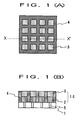
- Fig. 1(A) and Fig. 1(B) show one embodiment of the electrode structure of the present invention, wherein Fig. 1(A) is a plan view and Fig. 1(B) is a sectional view of Fig. 1(A) along the line X-X'.
- Fig. 2(A) shows the wiring for connection to a power supply in the electrode structure of Fig. 1 and Fig. 2(B) shows the connection between the wiring and a resistive element.
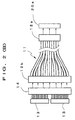
- Fig. 3 is a schematic view showing the electrode structure of the present invention during use.
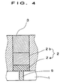
- Fig. 4 shows a preferable structure of the electrode constituting the electrode element of the inventive electrode structure.
- Figs. 5(A), 5(B) and 5(C) show another embodiment of the electrode structure of the present invention, wherein Fig. 5(A) is a plan view of one side of the insulating substrate, Fig. 5(B) is a sectional view of Fig. 5(A) along the line X-X' and Fig. 5(C) is a plan view of the other side of the insulating substrate.
- Fig. 6 is a schematic view showing a conventional electrode structure during use.
-
- The present invention is explained in detail in the following.
- The electrode structure of the present invention comprises plural electrode elements each comprising an electrode and an electrolyte layer laminated thereon. The plural electrode elements are insulated from each other. The electrolyte layer of each electrode element is brought into contact with the skin of a living body, and the electrode of each electrode element is connected to a power supply and electrically connected to a resistive element (resistive element having a resistance that is 1/5 - 5 times the resistance of the skin) that limits the current flowing through the electrode.
- Figs. 1, 2 show one embodiment of the inventive electrode structure. In this electrode structure, sixteen
electrode elements 10, each comprising anelectrode 2 and anelectrolyte layer 3 are disposed in a matrix configuration on one side (surface) of aninsulating substrate 1, and adjacent electrode elements are insulated from each other by apartition 4. Theinsulating substrate 1 has aconductive path 5 corresponding to eachelectrode element 10, and theelectrode 2 of eachelectrode element 10 is in contact with one end of theconductive path 5. - On the other side (back) of the
insulating substrate 1 is exposed the other end of eachconductive path 5, with which end one end of awiring 20 for connection to a power supply is connected. Thus, theelectrode 2 of eachelectrode element 10 is electrically connected to the power supply. - The
wiring 20 for connection to a power supply is laid on a tongue part 1a projecting from a part of theinsulating substrate 1 in the extending direction of the substrate, each end of the wire connecting to a connector 20a for wire extension, which is fixed on the tip of the tongue part 1a in the direction of the projection. The connector 20a has a configuration where two rows of terminals are disposed such that they are staggered in position, which configuration being called a half pitch connector to miniaturize the structure. - As shown in Fig. 2(B), the above-mentioned connector 20a is connected to a connector 12a on one end of an electric cable 11 for wire extension, and a resistive element
integration type connector 14 is connected to a connector 12b on the other end of the electric cable. The resistive elementintegration type connector 14 consists of twocollective resistors 13 each comprising eight resistive elements having a resistance that is 1/5 - 5 times the resistance of the skin, whereby each resistive element is connected to one of thewirings 20 for connection to a power supply. The connector 12a on one end of the electric cable 11 for wire extension is a half pitch connector corresponding to the connector 20a formed on the tongue part 1a of the insulatingsubstrate 1. - Fig. 3 shows the electrode structure of the present invention during use. As shown in this Figure, the electrode structure of the present invention is used by bringing the surface of the
electrolyte layer 3 of eachelectrode element 10 into contact with theskin 30, followed by electrification. As thepower supply 40, various power supplies can be used depending on the purpose. For example, a direct constant current power supply, pulse current power supply, high frequency power supply and the like can be used. - Each
electrode element 10 is insulated from other electrode elements by thepartition 4, so that the electrifying current does not flow between adjacent electrode elements (between electrode and electrode, between electrode and electrolyte layer, or between electrolyte layer and electrolyte layer). Inasmuch as theelectrode 2 of eachelectrode element 10 is electrically connected to aresistor 6 having a resistance that is 1/5 - 5 times the resistance of the skin, for example, the electrode element set on a wounded skin has lower contact resistance between the electrode element and the skin. Despite the tendency of the current to flow concentratedly through thiselectrode 2 of theelectrode element 10, the flow is limited by theresistor 6 having a resistance that is 1/5 - 5 times the resistance of the skin, and the concentrated flow of the current is prevented. - The
resistor 6 to be connected to theelectrode 2 of theelectrode element 10 is set to have a resistance that is 1/5 - 5 times the resistance of the skin, because the value smaller than 1/5 time the resistance of the skin shows insufficient effect of preventing concentration of the current and allows the current density to grow too high at a local site, thus creating a high risk of causing a burn, whereas when it is greater than 5 times, an excessive voltage is needed to obtain the current necessary for iontophoresis, diathermy knife and the like. The resistance of the human skin is about 5-100 kΩ/cm2 at a frequency of not greater than 100 Hz, which decreases with increasing frequencies, and becomes about several hundred Ω/cm2 at a frequency of not less than 100 kHz (see T. Yamamoto, Y. Yamamoto, "Electrical properties of the epidermal stratum corneum" Medical and Biological Engineering, March 1976, p. 151). - The material to be used for insulating
substrate 1 is free of limitation and any material can be used as long as it has an insulating property. Specific examples include polyimide, polyethylene terephthalate, polypropylene, polyamide and the like. From the aspects of heat resistance, moisture resistance and dimensional stability, polyimide and polyethylene terephthalate are preferably used. The shape of the insulatingsubstrate 1 is typically a sheet or a film. - The size and shape of the upper surface of the electrode element 10 (the surface of
electrolyte layer 3 that comes into contact with the skin) are not particularly limited and can be determined as appropriate depending on the living body to be the target, object, number of electrode elements and the like. It is generally preferable that the total area of the upper surface of theelectrode elements 10 be 2 - 400 cm2, preferably 4 - 200 cm2. - In the embodiment of Fig. 1, sixteen
electrode elements 10 have been disposed. The number of theelectrode elements 10 is preferably not less than 10, wherein more number thereof results in a highly constant current density. - The material of the
electrode 2 is subject to no particular limitation as long as it is conductive, and is exemplified by a film of conductive coating, metal foil and the like. - The conductive coating is exemplified by silver coating (e.g., DOTITE FA-353 manufactured by FUJIKURA KASEI CO., LTD.), carbon coating (e.g., carbon conductive coating MRX-713J manufactured by TAMURA CORPORATION) and the like. The metal foil is exemplified by foils of aluminum, copper, silver and the like. In the case of a conductive coating film, it may be formed directly on the insulating substrate, but a coating film may be also formed on a resin film, such as polyethylene terephthalate film and the like, and then a resin film having this coating film may be adhered solidly to the surface of an insulating substrate.
- While the
electrode 2 is a single layer in the embodiment of Fig. 1, a laminate consisting of the lower layer 2a and the upper layer 2b may be used, as shown in Fig. 4. By making the electrode a laminate, the electrode has an improved electrification property, and the electrode can be easily modified to give a construction that fits better for the electrode structure for a positive electrode or a negative electrode. - The lower layer 2a is preferably made from a material free of electrochemical changes. Such material is preferably a carbon. This carbon is preferably a coating film made from a composition (coating) containing fine carbon particles and a binder resin. The binder resin used here is exemplified by phenolic resin, polyester resin, epoxy resin, acrylic resin and the like. Such coating is exemplified by DOTITE FC-415 manufactured by FUJIKURA KASEI CO., LTD., carbon conductive coating MRX-713J manufactured by TAMURA CORPORATION and the like. The lower layer 2a comprising a carbon layer can be formed by, for example, screen printing.
- The upper layer 2b preferably contains a metal material having superior conductivity, such as silver. Examples of such layer include a silver-plated layer, a silver, silver chloride layer obtained by electrolysis of a silver-plated layer in brine, a coating film layer made from a coating containing fine silver powder and a binder resin, and a coating film layer made from a coating containing fine silver powder, fine silver chloride powder and a binder resin. As the binder resin, phenolic resin, polyester resin, epoxy resin, acrylic resin and the like can be used.
- When an electrode structure is used as a positive electrode, the upper layer 2b is preferably a silver-containing layer, which is exemplified by silver-plated layer and a coating film layer comprising a silver powder and a binder resin. When the electrode structure is used as a negative electrode, the upper layer 2b is preferably a silver, silver chloride-containing layer, which is exemplified by a coating film layer comprising a silver powder, a silver chloride powder and a binder resin, and a silver, silver chloride layer obtained by electrolysis of a silver-plated layer in brine.
- As the silver coating, DOTITE FA-353 manufactured by FUJIKURA KASEI CO., LTD. can be used and as the silver, silver chloride coating, DOTITE XA-450 manufactured by FUJIKURA KASEI CO., LTD. can be used. These coatings are screen printed to give the upper layer 2b made from a silver-containing layer or a silver, silver chloride-containing layer. The silver-containing layer and the silver, silver chloride-containing layer may be used as they are or after application of silver plating when the surface is desired to be 100% silver.
- The thickness of the upper layer made from a silver-containing layer or a silver, silver chloride-containing layer is subject to no particular limitation, but the amount to be attached needs to be more than the conversion amount of Ag→AgCl or AgCl→Ag, which is calculated from the electrification charge of iontophoresis.
- The surface shape of the
electrode 2 is subject to no particular limitation, but it is preferably a circle or polygon, wherein the area preferably does not exceed 1 cm2 for the prevention of concentration of the current. Theelectrode 2 is smaller than conventional single electrodes; hence it is preferably made into a 1-10 mm square in view of processability and handling property. When one side is smaller than 1 mm, processing becomes difficult, whereas when one side is greater than 10 mm, the density of the current electrified on the skin cannot be equalized easily. The thickness of theelectrode 2 is subject to no particular limitation, but it is generally about 10 - 100 µm, preferably about 20 - 50 µm. - The
electrolyte layer 3 to be laminated on theelectrode 2 consists of an electrolyte solution and a material capable of retaining this solution. Examples of the electrolyte solution include physiological saline or aqueous solution containing a drug capable of ionic dissociation. The material capable of retaining the electrolyte solution is subject to no particular limitation as long as it can retain the solution and may be, for example, absorbent cotton, sponge, gelling material and the like, with preference given to a gelling material that retains the electrolyte solution. - Examples of the gelling material include natural polysaccharides such as starch, karaya rubber, tragacanth rubber, xanthan gum and the like; vinyl resin such as poly(vinyl alcohol) obtained by partial saponification, poly(vinyl formal), poly(vinyl methyl ether) and copolymers thereof, poly(vinylpyrrolidone), poly(vinyl methacrylate) and the like; acrylic resin such as partially saponified polyacrylic ester, poly(acrylic acid-acrylamide) and the like; and the like. These natural polysaccharides and synthetic resins having hydrophilicity are softened with water and/or alcohol such as polyethylene glycol, glycerol and the like to give a flexible sheet gel having self-shape retention property and skin contactability. The thickness of the
electrolyte layer 3 is generally about 0.2-10 mm, preferably about 1-5 mm. - When the electrode structure of the present invention is used for iontophoresis, the drug-containing aqueous solution is contained in an
electrolyte layer 3 of the electrode structure for a positive electrode or a negative electrode, according to the ionic state of the drug in the aqueous solution. For example, when the drug is present as cations in the aqueous solution, it is used as an electrolyte solution contained in the electrolyte layer of the electrode structure for a positive electrode. When the drug is present as anions in the aqueous solution, it is used as an electrolyte solution contained in the electrolyte layer of the electrode structure for a negative electrode. In both cases, the electrolyte solution to be contained in the electrolyte layer of the other electrode structure is physiological saline. - The
partition 4 is subject to no particular limitation as long as it is made from a composition containing an insulating material. In view of the fact that the inventive electrode structure is adhered to the skin, it is preferably made from a composition containing an insulating material having flexibility. - The flexible insulating material may be, for example, soft silicone resin, styrene thermoplastic elastomer, olefin thermoplastic elastomer, propylene copolymerized soft resin and the like, with preference given to styrene thermoplastic elastomer having suitable flexibility. Examples of the styrene thermoplastic elastomer include RABALON SJ-4400 manufactured by Mitsubishi Chemical Corporation. It is also possible to use the same material as the insulating
substrate 1. - While the method for forming the
partition 4 and the shape thereof are subject to no particular limitation, it preferably has a shape allowing coherence to the side shape of eachelectrode element 10. As shown in Fig. 1(A), for example, when theelectrode element 10 is rectangular and the elements are aligned vertically and transversely, thepartition 4 preferably has a shape of a curb that allows coherence to the side shape of eachelectrode element 10. Thepartition 4 formed into a desired shape is set on the insulatingsubstrate 1 betweenelectrode elements 10 using an adhesive. - The
partition 4 may be integrally formed with the insulatingsubstrate 1. In this case, the part corresponding to the thickness of theelectrode 2 andelectrolyte layer 3 may be cut off from a thickinsulating substrate 1, or an integrated article of insulatingsubstrate 1 andpartition 4 may be formed using a mold. - The height of the
partition 4 may be any as long as theelectrolyte layer 3 does not overreach the partition, so that transverse diffusion of the current will not occur, which is preferably about 1-5 mm. The thickness of the partition is preferably not less than 0.1 mm. - Fig. 5 shows another embodiment of the electrode structure of the present invention. This electrode structure comprises a
resistive element 7 wherein a resistor having a resistance that is 1/5 - 5 times the resistance of the skin, which is to be electrically connected to theelectrode 2 of eachelectrode element 10, is set on the other side (back) of the insulatingsubstrate 1, and awiring layer 8 that connects eachresistive element 7 is set on the other side of the insulatingsubstrate 1, the wiring for connection to a power supply being connected to aterminal 9 formed on thiswiring layer 8. - Each
resistive element 7 is set on the other side (back) of the insulatingsubstrate 1 at the position corresponding to eachelectrode element 2, wherein themating electrode element 2 andresistive element 7 are electrically connected via aconductive path 5. Thewiring layer 8 forms a shape like teeth of a comb, allowing superposing part of eachresistive element 7, and has aterminal 9 on one end thereof. - The
resistive element 7 may be a commercial chip resistor. For lower production cost, however, a paste containing fine carbon particles and a binder resin may be formed into a shape affording a certain resistance by, for example, screen printing. The usable binder resin is exemplified by phenolic resin, polyester resin, epoxy resin, acrylic resin and the like. The paste is exemplified by DOTITE XC-155U manufactured by FUJIKURA KASEI CO., LTD. Thewiring layer 8 is formed by screen printing a conductive paste, such as a low resistant silver paste. Examples of the paste include DOTITE FA-353 manufactured by FUJIKURA KASEI CO., LTD. - According to the electrode structure of the present invention, the
conductive path 5 to be formed on the insulatingsubstrate 1 is prepared by forming a fine through hole in the insulatingsubstrate 1, and filling a conductive material therein. In this case, for example, a method comprising printing a carbon-containing coating on the insulatingsubstrate 1 having a through hole at a predetermined position to form a carbon layer to be the electrode 2 (lower layer 2a of the electrode) and concurrently packing a conductive material in the through hole, or a method comprising printing the back of the insulatingsubstrate 1 having a through hole at a predetermined position, with a carbon resistant paste for forming a resistive element to form aresistive element 7 and concurrently packing a conductive material in the through hole, may be employed. Theresistive element 7 andelectrode element 10 can be electrically connected with ease by these methods. - The present invention is explained in detail by illustrative reference examples and examples, to which the present invention is not limited in anyway.
- The electrode structure as shown in Figs. 1, 2 was used. The electrode used was a 17 µm thick, square (2.5 mm one side) copper foil plated with silver (5 µm), which was laminated on a polyimide film. The wiring was made of copper with an insulating coating applied thereon.
- A curb-like partition (width 1.5 mm,
height 2 mm) was made from a styrene thermoplastic elastomer (RABALON SJ-4400 manufactured by Mitsubishi Chemical Corporation) to separate the above-mentioned electrode elements at the distance of 1.5 mm and laminated on the polyimide film. - As the electrolyte layer, a conductive gel was used, which was prepared by impregnating, by 90 wt%, oblate (Drug Oblaat manufactured by NIIGATA OBLAAT CO., LTD.) with physiological saline (NaCl 0.9 wt%).
- A collective element consisting of 1 kΩ, 10 kΩ, 22 kΩ, 50 kΩ and 100 k Ω resistors was used, wherein each resistive element could be exchanged with a connector.
- As the direct constant current source, a portable constant current source circuit was used, which was newly prepared utilizing the constant current property of a transistor. For a pulse and high frequency power supply, a multifunction synthesizer type 1930 manufactured by NF CORPORATION was used.
- The voltage of the resistive element of the positive electrode and the negative electrode was measured by the NR-110 type data collection system manufactured by KEYENCE CORPORATION. The data were collected at 50-second intervals and the measurement data at 5 minutes after electrification were converted into current.
- To the left forearm of an adult male (measured resistance of the direct current area was about 7 kΩ/cm2) were applied electrode structures (containing 16 positive electrode elements and 16 negative electrode elements, each electrode 2.5 mm□), wherein the positive and negative electrode structures were set at a distance of 20 mm, and the structures were electrified. The resistive element for limiting the current had a resistance of 100 kΩ (converted into area unit resistance of 6.25 kΩ/cm2) and the density of the current flowing through each electrode element in the positive-negative electrode structure was calculated from the voltage applied to the both ends of the resistive element.
- In the same manner as in Example 1 except that the resistive element connected to each electrode element had a resistance of 50 kΩ (converted into area unit resistance of 3.125 kΩ/cm2), the density was calculated.
- In the same manner as in Example 1 except that the resistive element connected to each electrode element had a resistance of 22 kΩ (converted into area unit resistance of 1.375 kΩ/cm2), the density was calculated.
- In the same manner as in Example 1 except that the resistive element connected to each electrode element had a resistance of 10 kΩ (converted into area unit resistance of 625 Ω/cm2), the density was calculated.
- In the same manner as in Example 1 except that the resistive element connected to each electrode element had a resistance of 1 kΩ (converted into area unit resistance of 62.5 Ω/cm2), the density was calculated.
- The maximum value, the minimum value and the average value of the current density per each electrode element of the positive electrode structures as obtained in Examples 1-3 and Comparative Examples 1, 2 are shown in Table 1.
Unit: mA/electrode element Electrode No. Ex. 1 Ex. 2 Ex. 3 Com.Ex. 1 Com.Ex. 2 Electrode 10.064 0.065 0.065 0.063 0.062 Electrode 20.064 0.065 0.065 0.065 0.047 Electrode 30.065 0.065 0.070 0.064 0.058 Electrode 40.064 0.067 0.067 0.071 0.081 Electrode 50.065 0.066 0.070 0.065 0.068 Electrode 60.064 0.068 0.067 0.068 0.065 Electrode 70.066 0.066 0.072 0.065 0.058 Electrode 80.065 0.068 0.070 0.075 0.084 Electrode 90.065 0.067 0.069 0.072 0.084 Electrode 100.065 0.068 0.070 0.067 0.060 Electrode 11 0.065 0.067 0.073 0.070 0.069 Electrode 120.066 0.069 0.067 0.092 0.106 Electrode 130.065 0.066 0.064 0.065 0.059 Electrode 140.065 0.066 0.069 0.060 0.040 Electrode 15 0.065 0.067 0.067 0.070 0.080 Ave. current 0.065 0.067 0.068 0.069 0.068 Max. current 0.066 0.069 0.073 0.092 0.106 Min. current 0.064 0.065 0.064 0.060 0.040 - As shown in Table 1, with the resistor (1 kΩ) for limiting the current, the maximum value of the current density was 2.5 times the minimum value, whereas when the resistance for limiting the current was 22 kΩ, the current density showed dispersion of within about mean± 10%, with still less dispersion when the resistance for limiting the current was set to 50 kΩ and 100 kΩ.
- The skin (measured resistance in the direct current area about 5 kΩ /cm2) of a 5 month-old female Yucatan miniature swine purchased from CHARLES RIVER JAPAN INC. was cut in 5 cm × 10 cm, and physiological saline was placed on the skin enclosed in a 1% agar gel. In the same manner as in Example 1 with regard to the size, number and position of each electrode element, resistance of resistive element and the like, the current density was measured.
- In the same manner as in Example 4 except that the resistive element connected to each electrode element had a resistance of 1 kΩ (converted into area unit resistance of 62.5 Ω/cm2), the current density was measured.
- The maximum value, the minimum value and the average value of the current density per each electrode element of the positive electrode structures as obtained in Example 4 and Comparative Example 3 are shown in Table 2.
Unit: mA/electrode element Electrode No. Ex. 4 Comp.Ex. 3 Electrode 10.036 0.053 Electrode 20.034 0.044 Electrode 30.035 0.047 Electrode 40.033 0.050 Electrode 50.033 0.030 Electrode 60.033 0.044 Electrode 70.034 0.042 Electrode 80.034 0.056 Electrode 90.032 0.027 Electrode 100.032 0.051 Electrode 11 0.034 0.052 Electrode 120.031 0.032 Electrode 130.035 0.034 Electrode 140.033 0.044 Electrode 15 0.035 0.058 Ave. current 0.034 0.041 Max. current 0.036 0.058 Min. current 0.031 0.027 - As shown in Table 2, with the resistor (1 kΩ) for limiting the current as shown in Comparative Example 3, the maximum value of the current density was about 2 times the minimum value, whereas when the resistance for limiting the current was 100 kΩ as in Example 4, the current density showed dispersion of within about mean± 10%.
- In the same manner as in Example 4, except that the skin of the 5 month-old female Yucatan miniature swine purchased from CHARLES RIVER JAPAN INC. was punctured with an about 0.8 mm⊘ needle to make a hole, the current density was measured.
- In the same manner as in Example 5 except that the resistive element connected to each electrode element had a resistance of 1 kΩ (converted into area unit resistance of 62.5 Ω/cm2), the current density was measured.
- The maximum value, the minimum value and the average value of the current density per each electrode element of the positive electrodes as obtained in Example 5 and Comparative Example 4 are shown in Table 3.
Unit: mA/electrode element Electrode No. Ex. 5 Comp.Ex. 4 Electrode 10.035 0.061 Electrode 20.033 0.046 Electrode 30.034 0.051 Electrode 40.033 0.041 Electrode 50.033 0.038 Electrode 60.032 0.034 Electrode 70.033 0.040 Electrode 80.033 0.038 Electrode 90.032 0.039 Electrode 100.032 0.030 Electrode 11 0.034 0.044 Electrode 120.033 0.043 Electrode 130.034 0.051 Electrode 140.031 0.029 Electrode 15 0.034 0.062 Ave. current 0.033 0.043 Max. current 0.035 0.062 Min. current 0.031 0.029 - As shown in Table 3, in the case of a damaged skin with the resistor for limiting the current of 1 kΩ as shown in Comparative Example 4, the maximum value of the current density was about 2 times the minimum value, whereas when the resistance for limiting the current was 100 kΩ as in Example 5, the current density showed dispersion of within about mean± 10%. Thus, as in the case of the skin without a wound, decrease in the resistance could be suppressed even in the case of the damaged skin.
- Two electrode structures shown in Fig. 5 for the positive electrode side and the negative electrode side were prepared as in the following.
- A 0.3 mm⊘ through hole was formed in a 50 µm polyester film substrate at the predetermined position where a carbon layer (lower layer 2a of electrode 2) was to be formed, and carbon conductive coating (FC-415 manufactured by FUJIKURA KASEI CO., LTD.) was screen printed in a thickness of 10 µm, whereby 16 carbon layers (each size 3.5 mm□, each interval 1.5 mm) were formed.
- On the back of the film, a carbon resistant paste (XC-155U manufactured by FUJIKURA KASEI CO., LTD.) was screen printed to form a
resistive element 7 having a resistance of about 50 kΩ (12.5 kΩ /cm2 was the designed value in this example) at the position corresponding to the position where the carbon layer was to be formed. Concurrently, the through hole was filled with the paste to give aconductive path 5, via which the carbon layer and the resistive element were electrically connected. Then, a wiring to connect these resistive elements was formed by screen printing of a silver paste (FA-353, manufactured by FUJIKURA KASEI CO., LTD.). - Then, on the above-mentioned carbon layer, a 30 µm thick silver paste (FA-353, manufactured by FUJIKURA KASEI CO., LTD.) was screen printed to give a silver-containing layer (upper layer 2b of electrode 2) for the positive electrode, and a silver, silver chloride paste (XA-450, manufactured by FUJIKURA KASEI CO., LTD.) was screen printed to give a silver, silver chloride-containing layer for the negative electrode, whereby an
electrode 2 was formed. - A curb-like electrode partition (
width 1 mm,height 2 mm,pitch 5 mm) that adhered to the side shape of the electrode was formed from a styrene thermoplastic elastomer (RABALON SJ-4400 manufactured by Mitsubishi Chemical Corporation). Thispartition 4 was fit in between the electrodes on the above-mentioned insulating substrate and adhered to the insulating substrate with an epoxy resin. - As the
electrolyte layer 3 for the positive electrode, a gel prepared by impregnating, by 90 wt%, oblate (Drug Oblaat manufactured by NIIGATA OBLAAT CO., LTD.) with 10 wt% aqueous lidocaine hydrochloride solution was used, and as theelectrolyte layer 3 for the negative electrode, a gel prepared by impregnating, by 90 wt%, oblate (Drug Oblaat manufactured by NIIGATA OBLAAT CO., LTD.) with 0.9 wt% physiological saline was used to respectively form layers on the silver-containing layer and the silver, silver chloride-containing layer. - As shown in Fig. 3, the obtained electrode structures on the positive electrode side and the negative electrode side were adhered to the left forearm of an adult male (skin resistance about 15 kΩ/cm2) at about 20 mm interval, and electrified with direct constant current (2 mA) for 10 minutes.
- The electrode structure as shown in Fig. 6 was prepared as in the following.
- The
single electrode 21 was a silver foil electrode (20 mm□,thickness 30 µm), and a silver chloride layer 22 having a thickness of about 5 µm was formed on thesingle electrode 21 on the negative electrode side. - An
electrolyte layer 23 on the positive electrode side was formed by impregnating about 2 mm thick absorbent cotton with a 10 wt% aqueous lidocaine hydrochloride solution, and anelectrolyte layer 23 on the negative electrode side was formed by impregnating about 2 mm thick absorbent cotton with 0.9 wt% physiological saline. - The obtained electrode structures on the positive electrode side and the negative electrode side were adhered to the left forearm of an adult male (skin resistance about 15 kΩ /cm2) at about 20 mm interval as shown in Fig. 3, and electrified with direct constant current (2 mA) for 10 minutes.
- As a result of the electrification, the positive electrode side showed a sufficient local anesthesia effect of lidocaine in both Example 6 and Comparative Example 5. Blister due to the concentration of the current was not found in Example 6, but in Comparative Example 5, both the positive electrode side and the negative electrode side showed about 2 mm⊘ blister due to the local current concentration.
- The electrode structure for positive electrode and the electrode structure for negative electrode obtained in Example 6 were adhered to the left forearm of an adult male (skin resistance about 15 kΩ/cm2) at about 20 mm interval as shown in Fig. 3, and electrified with direct constant current (1.6 mA) for 5 minutes. As the direct constant current source, a portable constant current source circuit was used, which was newly prepared utilizing the constant current property of a transistor. The current density was determined from the voltage applied to the
resistive element 7 of each electrode element. The measurement data at 5 minutes after electrification were converted into current. - In the same manner as in Example 7 except that the coating thickness of the carbon resistant paste was changed to make the resistance of the resistive element about 10 kΩ (2.5 kΩ/cm2), electrode structures for the positive electrode and negative electrode were prepared, and the current density was measured.
- The maximum value, the minimum value and the average value of the current density per each electrode element of the positive electrode structures as obtained in Example 7 and Comparative Example 6 are shown in Table 4.
Unit: mA/electrode element Electrode No. Ex. 7 Comp.Ex. 6 Electrode 10.105 0.104 Electrode 20.105 0.072 Electrode 30.11 0.068 Electrode 40.109 0.083 Electrode 50.102 0.108 Electrode 60.101 0.118 Electrode 70.11 0.071 Electrode 80.107 0.049 Electrode 90.109 0.092 Electrode 100.111 0.081 Electrode 11 0.111 0.139 Electrode 120.099 0.357 Electrode 130.114 0.071 Electrode 140.106 0.097 Electrode 15 0.107 0.073 Ave. current 0.107 0.106 Max. current 0.114 0.357 Min. current 0.099 0.049 - As shown in Table 4, the current density showed dispersion of within about mean± 10% in Example 7. However, in Comparative Example 6, the current density was not constant due to the low resistance.
Claims (14)
- An electrode structure comprising plural electrode elements each comprising an electrode and an electrolyte layer laminated thereon, the electrode of each electrode element being connected to a power supply and the electrolyte layer to be in contact with the skin,
wherein the plural electrode elements are insulated from each other and the electrode of each element is electrically connected to a resistor that limits the current flowing through this electrode, said resistor having a resistance that is 1/5 - 5 times the resistance of the skin. - The electrode structure of claim 1, wherein the electrode elements are insulated from each other on an insulating substrate by the aid of a partition, and the electrode of each electrode element has a resistive element having a resistance that is 1/5 - 5 times the resistance of the skin.
- The electrode structure of claim 2, wherein each electrode element is disposed on one side of the insulating substrate and insulated from other electrode elements by a partition, and wherein the resistive element having a resistance that is 1/5 - 5 times the resistance of the skin is disposed on the other side of the insulating substrate at the position corresponding to a mating electrode element, each electrode of the electrode element and the corresponding resistive element being electrically connected via a conductive path formed in the insulating substrate.
- The electrode structure of claim 3, wherein the insulating substrate has a wiring layer on said other side of the substrate, the wiring layer being connected to a part of the corresponding resistive element, and having a terminal connecting a wiring for connection to a power supply.
- The electrode structure of claim 2, wherein each electrode element is disposed on one side of the insulating substrate and insulated from other electrode elements by a partition, the electrode of each electrode element is electrically connected, on the other side of the insulating substrate, to a wiring for connection to a power supply via a conductive path formed in the insulating substrate, and the wiring is connected to a resistive element having a resistance that is 1/5 - 5 times the resistance of the skin.
- The electrode structure of claim 5, wherein the wiring is laid on a tongue part projecting from a part of the insulating substrate in the extending direction of the substrate, each end of the wire being connected to the connector for wire extension fixed on the tip of the tongue part,
wherein the connector for wire extension is connected to a connector on one end of an electric cable for wire extension, and an integration type connector equipped with resistive elements having a resistance that is 1/5 - 5 times the resistance of the skin is connected to a connector on the other end of the electric cable, thereby electrically connecting the resistive elements to the wiring. - The electrode structure of any of claims 1, 2, 3 and 5, wherein the electrode of each electrode element has a circular or polygonal shape and an area of less than 1 cm2.
- The electrode structure of any of claims 1, 2, 3 and 5, wherein the electrode of each electrode element comprises a carbon layer and a silver-containing layer formed on the carbon layer.
- The electrode structure of any of claims 1, 2, 3 and 5, wherein the electrode of each electrode element comprises a carbon layer and a silver, silver chloride-containing layer formed on the carbon layer.
- The electrode structure of claim 8 or claim 9, wherein the carbon layer comprises a composition comprising fine carbon particles and a binder resin.
- The electrode structure of claim 3, wherein the resistive element comprises a composition comprising fine carbon particles and a binder resin.
- The electrode structure of any of claims 2, 3 and 5, wherein the partition is made from a flexible insulating material.
- The electrode structure of any of claims 2, 3 and 5, wherein the partition has a shape permitting adhesion to the side of each electrode element and is a formed article having a thickness of not less than 0.1 mm and a height of 1 - 5 mm.
- The electrode structure of any of claims 2, 3 and 5, wherein the partition and the insulating substrate form an integrated product.
Applications Claiming Priority (4)
| Application Number | Priority Date | Filing Date | Title |
|---|---|---|---|
| JP10193387A JP2000024121A (en) | 1998-07-08 | 1998-07-08 | Electrode structure |
| JP19338798 | 1998-07-08 | ||
| JP10357957A JP2000176024A (en) | 1998-12-16 | 1998-12-16 | Electrode structural body |
| JP35795798 | 1998-12-16 |
Publications (2)
| Publication Number | Publication Date |
|---|---|
| EP0970719A2 true EP0970719A2 (en) | 2000-01-12 |
| EP0970719A3 EP0970719A3 (en) | 2000-08-23 |
Family
ID=26507851
Family Applications (1)
| Application Number | Title | Priority Date | Filing Date |
|---|---|---|---|
| EP99113028A Withdrawn EP0970719A3 (en) | 1998-07-08 | 1999-07-06 | Electrode structure |
Country Status (2)
| Country | Link |
|---|---|
| US (1) | US6336049B1 (en) |
| EP (1) | EP0970719A3 (en) |
Cited By (5)
| Publication number | Priority date | Publication date | Assignee | Title |
|---|---|---|---|---|
| DE102006050369A1 (en) * | 2006-10-25 | 2008-04-30 | Oncotherm Kft. | Hyperthermia device for the selective treatment and monitoring of surface tissue |
| WO2008157481A1 (en) * | 2007-06-15 | 2008-12-24 | Transport Pharmaceuticals, Inc. | Method and system for mitigating current concentration in electrokinetic drug delivery |
| WO2016087646A1 (en) * | 2014-12-04 | 2016-06-09 | Ant Applied Neuroscience Technologies Gmbh | Electrode for electrostimulation |
| WO2016155878A1 (en) * | 2015-03-28 | 2016-10-06 | Albrecht Molsberger | Direct current applicator for therapeutic use, with a plurality of sheet-like structures |
| WO2016177780A1 (en) * | 2015-05-05 | 2016-11-10 | Feeligreen | Support for electrophoresis and/or iontophoresis |
Families Citing this family (50)
| Publication number | Priority date | Publication date | Assignee | Title |
|---|---|---|---|---|
| JP3863391B2 (en) * | 2001-06-13 | 2006-12-27 | Necエレクトロニクス株式会社 | Semiconductor device |
| JP4272532B2 (en) * | 2002-01-14 | 2009-06-03 | シーメンス ヴィディーオー オートモティヴ コーポレイション | Tire pressure monitoring system that responds to the transition of a vehicle from a stationary state to a moving state |
| EP1484084A4 (en) * | 2002-01-24 | 2009-12-23 | Hisamitsu Pharmaceutical Co | Electrode structure |
| DE10205373B4 (en) * | 2002-02-09 | 2007-07-19 | Aloys Wobben | Fire protection |
| US7437201B2 (en) * | 2003-01-14 | 2008-10-14 | Cullen Christopher P | Electric motor controller |
| JP2005116615A (en) * | 2003-10-03 | 2005-04-28 | Dowa Mining Co Ltd | Semiconductor light emitting element and its manufacturing method |
| US7588856B2 (en) | 2004-08-04 | 2009-09-15 | Corning Incorporated | Resistive-varying electrode structure |
| US20060095001A1 (en) * | 2004-10-29 | 2006-05-04 | Transcutaneous Technologies Inc. | Electrode and iontophoresis device |
| US20060135906A1 (en) * | 2004-11-16 | 2006-06-22 | Akihiko Matsumura | Iontophoretic device and method for administering immune response-enhancing agents and compositions |
| JP2006346368A (en) * | 2005-06-20 | 2006-12-28 | Transcutaneous Technologies Inc | Iontophoresis apparatus and manufacturing method |
| JP2007000342A (en) * | 2005-06-23 | 2007-01-11 | Transcutaneous Technologies Inc | Iontophoresis device for controlling quantity and time of dosing a plurality of medicaments |
| US8295922B2 (en) | 2005-08-08 | 2012-10-23 | Tti Ellebeau, Inc. | Iontophoresis device |
| US8386030B2 (en) * | 2005-08-08 | 2013-02-26 | Tti Ellebeau, Inc. | Iontophoresis device |
| US20070088332A1 (en) * | 2005-08-22 | 2007-04-19 | Transcutaneous Technologies Inc. | Iontophoresis device |
| JPWO2007023907A1 (en) * | 2005-08-24 | 2009-02-26 | Tti・エルビュー株式会社 | Electrode structure for frozen iontophoresis |
| US20070048362A1 (en) * | 2005-08-29 | 2007-03-01 | Transcutaneous Technologies Inc. | General purpose electrolyte solution composition for iontophoresis |
| US20100030128A1 (en) * | 2005-09-06 | 2010-02-04 | Kazuma Mitsuguchi | Iontophoresis device |
| US20070112294A1 (en) * | 2005-09-14 | 2007-05-17 | Transcutaneous Technologies Inc. | Iontophoresis device |
| JPWO2007032446A1 (en) * | 2005-09-15 | 2009-03-19 | Tti・エルビュー株式会社 | Rod iontophoresis device |
| US20090216177A1 (en) * | 2005-09-16 | 2009-08-27 | Tti Ellebeau,Inc | Catheter-type iontophoresis device |
| WO2007037324A1 (en) * | 2005-09-28 | 2007-04-05 | Transcu Ltd. | Dry electrode construct for iontophoresis |
| WO2007041115A1 (en) * | 2005-09-30 | 2007-04-12 | Tti Ellebeau Inc. | Method and system to detect malfunctions in an iontophoresis device that delivers active agents to biological interfaces |
| US20090299265A1 (en) * | 2005-09-30 | 2009-12-03 | Tti Ellebeau, Inc. | Electrode Assembly for Iontophoresis Having Shape-Memory Separator and Iontophoresis Device Using the Same |
| US20070083186A1 (en) * | 2005-09-30 | 2007-04-12 | Darrick Carter | Transdermal drug delivery systems, devices, and methods employing novel pharmaceutical vehicles |
| EP1928539A1 (en) * | 2005-09-30 | 2008-06-11 | Tti Ellebeau, Inc. | Functionalized microneedles transdermal drug delivery systems, devices, and methods |
| BRPI0616771A2 (en) * | 2005-09-30 | 2011-06-28 | Tti Ellebeau Inc | iontophoresis device to release multiple active agents for biological interfaces |
| WO2007041323A1 (en) * | 2005-09-30 | 2007-04-12 | Tti Ellebeau, Inc. | Iontophoretic delivery of vesicle-encapsulated active agents |
| EP1944057A4 (en) * | 2005-09-30 | 2009-02-18 | Tti Ellebeau Inc | Iontophoresis apparatus capable of controlling dose and timing of administration of sleep inducer and analeptic agent |
| US20070232983A1 (en) * | 2005-09-30 | 2007-10-04 | Smith Gregory A | Handheld apparatus to deliver active agents to biological interfaces |
| US20070135754A1 (en) * | 2005-09-30 | 2007-06-14 | Hidero Akiyama | Electrode assembly for iontophoresis for administering active agent enclosed in nanoparticle and iontophoresis device using the same |
| US20070197955A1 (en) * | 2005-10-12 | 2007-08-23 | Transcutaneous Technologies Inc. | Mucous membrane adhesion-type iontophoresis device |
| US20080033338A1 (en) * | 2005-12-28 | 2008-02-07 | Smith Gregory A | Electroosmotic pump apparatus and method to deliver active agents to biological interfaces |
| WO2007079190A2 (en) * | 2005-12-29 | 2007-07-12 | Tti Ellebeau, Inc. | Device and method for enhancing immune response by electrical stimulation |
| MX2009002321A (en) * | 2006-09-05 | 2009-03-23 | Tti Ellebeau Inc | Transdermal drug delivery systems, devices, and methods using inductive power supplies. |
| JP5383497B2 (en) | 2006-12-01 | 2014-01-08 | Tti・エルビュー株式会社 | System and device for powering and / or controlling a device, for example a transdermal delivery device |
| US7996055B2 (en) * | 2006-12-29 | 2011-08-09 | St. Jude Medical, Atrial Fibrillation Division, Inc. | Cardiac navigation system including electrode array for use therewith |
| US7957784B2 (en) * | 2006-12-29 | 2011-06-07 | St. Jude Medical, Atrial Fibrillation Division, Inc. | Body surface mapping system |
| US20080188791A1 (en) * | 2007-02-02 | 2008-08-07 | Difiore Attilio E | Active iontophoresis delivery system |
| WO2008141221A1 (en) * | 2007-05-09 | 2008-11-20 | Old Dominion University Research Foundation | Suction electrode-based medical instrument and system including the medical instrument for therapeutic electrotherapy |
| US8197844B2 (en) * | 2007-06-08 | 2012-06-12 | Activatek, Inc. | Active electrode for transdermal medicament administration |
| DE102007034796B4 (en) * | 2007-07-25 | 2016-01-07 | Wellcomet Gmbh | Device for generating high-frequency currents, for the cosmetic and / or therapeutic treatment of tissue by means of electrodes |
| US8862223B2 (en) | 2008-01-18 | 2014-10-14 | Activatek, Inc. | Active transdermal medicament patch and circuit board for same |
| AT507855A1 (en) * | 2009-01-20 | 2010-08-15 | Lang Leonh | bioelectrode |
| TW201121604A (en) * | 2009-06-09 | 2011-07-01 | Tti Ellebeau Inc | Long life high capacity electrode, device, and method of manufacture |
| US8299371B2 (en) * | 2010-12-20 | 2012-10-30 | Endicott Interconnect Technologies, Inc. | Circuitized substrate with dielectric interposer assembly and method |
| AU2011345942B2 (en) | 2010-12-22 | 2016-03-10 | Teikoku Seiyaku Co., Ltd. | Electrode pad for iontophoresis |
| EP3468659A4 (en) | 2016-06-09 | 2020-01-15 | The Board of Trustees of the Leland Stanford Junior University | Devices for delivery of electrical current to the body and related methods for therapy |
| WO2018132298A1 (en) * | 2017-01-11 | 2018-07-19 | Vomaris Innovations, Inc. | Dressing application systems and devices |
| USD854186S1 (en) * | 2017-09-13 | 2019-07-16 | Precision Dynamics Corporation | CT gantry shield |
| US11433230B2 (en) | 2019-01-16 | 2022-09-06 | palmm Co. | Devices, systems, and methods for delivering electrical current to the body |
Citations (3)
| Publication number | Priority date | Publication date | Assignee | Title |
|---|---|---|---|---|
| US4416274A (en) | 1981-02-23 | 1983-11-22 | Motion Control, Inc. | Ion mobility limiting iontophoretic bioelectrode |
| US4950229A (en) | 1989-09-25 | 1990-08-21 | Becton, Dickinson And Company | Apparatus for an electrode used for iontophoresis |
| US5310403A (en) | 1992-05-18 | 1994-05-10 | Becton, Dickinson And Company | Iontophoretic drug delivery device and circuit therefor |
Family Cites Families (11)
| Publication number | Priority date | Publication date | Assignee | Title |
|---|---|---|---|---|
| US4141359A (en) * | 1976-08-16 | 1979-02-27 | University Of Utah | Epidermal iontophoresis device |
| US4622031A (en) * | 1983-08-18 | 1986-11-11 | Drug Delivery Systems Inc. | Indicator for electrophoretic transcutaneous drug delivery device |
| US4919648A (en) * | 1983-08-18 | 1990-04-24 | Drug Delivery Systems Inc. | High tack drug patch |
| WO1986007269A1 (en) * | 1985-06-10 | 1986-12-18 | Drug Delivery Systems Inc. | Programmable control and mounting system for transdermal drug applicator |
| IL86076A (en) * | 1988-04-14 | 1992-12-01 | Inventor S Funding Corp Ltd | Transdermal drug delivery device |
| US5147297A (en) * | 1990-05-07 | 1992-09-15 | Alza Corporation | Iontophoretic delivery device |
| DE4114677A1 (en) * | 1990-10-10 | 1992-02-27 | Mario Bergner | APPLICATION ARRANGEMENT OF DIFFERENT ELECTRICALLY CONNECTED METALS ON THE HUMAN BODY TO A BIOELECTRIC SYSTEM IN THE MEANING OF THE ELECTROCHEMICAL VOLTAGE RANGE WITH VOLTAGE INCREASING WITH POSSIBLE USE OF COMMERCIAL ECG FLASHER ELEMENTS |
| US5295482A (en) * | 1992-10-22 | 1994-03-22 | Physiometrix, Inc. | Large surface area electrode |
| US5380272A (en) * | 1993-01-28 | 1995-01-10 | Scientific Innovations Ltd. | Transcutaneous drug delivery applicator |
| US5857994A (en) * | 1996-10-01 | 1999-01-12 | Becton, Dickinson And Company | Awakenable iontophoretic/delivery device for reducing electrical sensation upon application thereof |
| US6078842A (en) * | 1997-04-08 | 2000-06-20 | Elan Corporation, Plc | Electrode and iontophoretic device and method |
-
1999
- 1999-07-06 EP EP99113028A patent/EP0970719A3/en not_active Withdrawn
- 1999-07-07 US US09/348,756 patent/US6336049B1/en not_active Expired - Fee Related
Patent Citations (4)
| Publication number | Priority date | Publication date | Assignee | Title |
|---|---|---|---|---|
| US4416274A (en) | 1981-02-23 | 1983-11-22 | Motion Control, Inc. | Ion mobility limiting iontophoretic bioelectrode |
| US4950229A (en) | 1989-09-25 | 1990-08-21 | Becton, Dickinson And Company | Apparatus for an electrode used for iontophoresis |
| US5284471A (en) | 1989-09-25 | 1994-02-08 | Becton, Dickinson And Company | Electrode and method used for iontophoresis |
| US5310403A (en) | 1992-05-18 | 1994-05-10 | Becton, Dickinson And Company | Iontophoretic drug delivery device and circuit therefor |
Cited By (6)
| Publication number | Priority date | Publication date | Assignee | Title |
|---|---|---|---|---|
| DE102006050369A1 (en) * | 2006-10-25 | 2008-04-30 | Oncotherm Kft. | Hyperthermia device for the selective treatment and monitoring of surface tissue |
| WO2008157481A1 (en) * | 2007-06-15 | 2008-12-24 | Transport Pharmaceuticals, Inc. | Method and system for mitigating current concentration in electrokinetic drug delivery |
| WO2016087646A1 (en) * | 2014-12-04 | 2016-06-09 | Ant Applied Neuroscience Technologies Gmbh | Electrode for electrostimulation |
| WO2016155878A1 (en) * | 2015-03-28 | 2016-10-06 | Albrecht Molsberger | Direct current applicator for therapeutic use, with a plurality of sheet-like structures |
| WO2016177780A1 (en) * | 2015-05-05 | 2016-11-10 | Feeligreen | Support for electrophoresis and/or iontophoresis |
| FR3035792A1 (en) * | 2015-05-05 | 2016-11-11 | Feeligreen | SUPPORT FOR ELECTROPHORESIS AND / OR IONTOPHORESIS |
Also Published As
| Publication number | Publication date |
|---|---|
| US6336049B1 (en) | 2002-01-01 |
| EP0970719A3 (en) | 2000-08-23 |
Similar Documents
| Publication | Publication Date | Title |
|---|---|---|
| US6336049B1 (en) | Electrode structure for reducing irritation to the skin | |
| JP4708447B2 (en) | Floating electrode | |
| CA2022824C (en) | Apparatus for an electrode and method used for iontophoresis | |
| EP0147524B1 (en) | Applicator for the non-invasive transcutaneous delivery of medicament | |
| CA2002849C (en) | Method and apparatus for iontophoretic drug delivery | |
| CA1093158A (en) | Disposable electrode | |
| CA1203286A (en) | Bioelectrode | |
| JP4262410B2 (en) | Electrical transmission electrode assembly with low initial resistance | |
| US5904712A (en) | Current-controlling electrode | |
| AU742396B2 (en) | Electrode for transferring an electric current through a patient's skin | |
| KR940000071B1 (en) | Transdermal drug applicator | |
| US6731977B2 (en) | Iontophoretic electrode with improved current distribution | |
| JP3149949B2 (en) | Ion introduction delivery device | |
| JP4221151B2 (en) | Electrochemically reactive cathode for electron transport devices. | |
| US4243051A (en) | Disposable electrode | |
| JPH05505955A (en) | Iontophoretic administration device | |
| JPH07507465A (en) | Iontophoretic drug administration device | |
| WO1992004937A1 (en) | Iontophoretic drug delivery apparatus | |
| KR20080044259A (en) | Iontophoresis device | |
| EP1463560A1 (en) | Reservoir housing having a conductive region integrally formed therein | |
| JP2001190693A (en) | Electrode structural body | |
| JP2000176024A (en) | Electrode structural body | |
| JP2000024121A (en) | Electrode structure | |
| JPH0232892B2 (en) | ||
| JP2001190694A (en) | Biomedical electrode structural body |
Legal Events
| Date | Code | Title | Description |
|---|---|---|---|
| PUAI | Public reference made under article 153(3) epc to a published international application that has entered the european phase |
Free format text: ORIGINAL CODE: 0009012 |
|
| AK | Designated contracting states |
Kind code of ref document: A2 Designated state(s): AT BE CH CY DE DK ES FI FR GB GR IE IT LI LU MC NL PT SE |
|
| AX | Request for extension of the european patent |
Free format text: AL;LT;LV;MK;RO;SI |
|
| PUAL | Search report despatched |
Free format text: ORIGINAL CODE: 0009013 |
|
| AK | Designated contracting states |
Kind code of ref document: A3 Designated state(s): AT BE CH CY DE DK ES FI FR GB GR IE IT LI LU MC NL PT SE |
|
| AX | Request for extension of the european patent |
Free format text: AL;LT;LV;MK;RO;SI |
|
| 17P | Request for examination filed |
Effective date: 20000922 |
|
| AKX | Designation fees paid |
Free format text: AT BE CH CY DE DK ES FI FR GB GR IE IT LI LU MC NL PT SE |
|
| 17Q | First examination report despatched |
Effective date: 20030624 |
|
| STAA | Information on the status of an ep patent application or granted ep patent |
Free format text: STATUS: THE APPLICATION IS DEEMED TO BE WITHDRAWN |
|
| 18D | Application deemed to be withdrawn |
Effective date: 20031230 |