EP0975010A1 - Prevention of photoresist poisoning from dielectric antireflective coating in semiconductor fabrication - Google Patents
Prevention of photoresist poisoning from dielectric antireflective coating in semiconductor fabrication Download PDFInfo
- Publication number
- EP0975010A1 EP0975010A1 EP99113532A EP99113532A EP0975010A1 EP 0975010 A1 EP0975010 A1 EP 0975010A1 EP 99113532 A EP99113532 A EP 99113532A EP 99113532 A EP99113532 A EP 99113532A EP 0975010 A1 EP0975010 A1 EP 0975010A1
- Authority
- EP
- European Patent Office
- Prior art keywords
- layer
- photoresist
- dielectric spacer
- silicon oxynitride
- dielectric
- Prior art date
- Legal status (The legal status is an assumption and is not a legal conclusion. Google has not performed a legal analysis and makes no representation as to the accuracy of the status listed.)
- Withdrawn
Links
Images

Classifications
-
- H—ELECTRICITY
- H01—ELECTRIC ELEMENTS
- H01L—SEMICONDUCTOR DEVICES NOT COVERED BY CLASS H10
- H01L21/00—Processes or apparatus adapted for the manufacture or treatment of semiconductor or solid state devices or of parts thereof
- H01L21/02—Manufacture or treatment of semiconductor devices or of parts thereof
- H01L21/027—Making masks on semiconductor bodies for further photolithographic processing not provided for in group H01L21/18 or H01L21/34
- H01L21/0271—Making masks on semiconductor bodies for further photolithographic processing not provided for in group H01L21/18 or H01L21/34 comprising organic layers
- H01L21/0273—Making masks on semiconductor bodies for further photolithographic processing not provided for in group H01L21/18 or H01L21/34 comprising organic layers characterised by the treatment of photoresist layers
- H01L21/0274—Photolithographic processes
- H01L21/0276—Photolithographic processes using an anti-reflective coating
-
- H—ELECTRICITY
- H01—ELECTRIC ELEMENTS
- H01L—SEMICONDUCTOR DEVICES NOT COVERED BY CLASS H10
- H01L21/00—Processes or apparatus adapted for the manufacture or treatment of semiconductor or solid state devices or of parts thereof
- H01L21/70—Manufacture or treatment of devices consisting of a plurality of solid state components formed in or on a common substrate or of parts thereof; Manufacture of integrated circuit devices or of parts thereof
- H01L21/71—Manufacture of specific parts of devices defined in group H01L21/70
- H01L21/768—Applying interconnections to be used for carrying current between separate components within a device comprising conductors and dielectrics
-
- H—ELECTRICITY
- H01—ELECTRIC ELEMENTS
- H01L—SEMICONDUCTOR DEVICES NOT COVERED BY CLASS H10
- H01L21/00—Processes or apparatus adapted for the manufacture or treatment of semiconductor or solid state devices or of parts thereof
- H01L21/02—Manufacture or treatment of semiconductor devices or of parts thereof
- H01L21/04—Manufacture or treatment of semiconductor devices or of parts thereof the devices having at least one potential-jump barrier or surface barrier, e.g. PN junction, depletion layer or carrier concentration layer
- H01L21/18—Manufacture or treatment of semiconductor devices or of parts thereof the devices having at least one potential-jump barrier or surface barrier, e.g. PN junction, depletion layer or carrier concentration layer the devices having semiconductor bodies comprising elements of Group IV of the Periodic System or AIIIBV compounds with or without impurities, e.g. doping materials
- H01L21/30—Treatment of semiconductor bodies using processes or apparatus not provided for in groups H01L21/20 - H01L21/26
- H01L21/31—Treatment of semiconductor bodies using processes or apparatus not provided for in groups H01L21/20 - H01L21/26 to form insulating layers thereon, e.g. for masking or by using photolithographic techniques; After treatment of these layers; Selection of materials for these layers
- H01L21/3105—After-treatment
- H01L21/311—Etching the insulating layers by chemical or physical means
- H01L21/31144—Etching the insulating layers by chemical or physical means using masks
-
- H—ELECTRICITY
- H01—ELECTRIC ELEMENTS
- H01L—SEMICONDUCTOR DEVICES NOT COVERED BY CLASS H10
- H01L21/00—Processes or apparatus adapted for the manufacture or treatment of semiconductor or solid state devices or of parts thereof
- H01L21/70—Manufacture or treatment of devices consisting of a plurality of solid state components formed in or on a common substrate or of parts thereof; Manufacture of integrated circuit devices or of parts thereof
- H01L21/71—Manufacture of specific parts of devices defined in group H01L21/70
- H01L21/768—Applying interconnections to be used for carrying current between separate components within a device comprising conductors and dielectrics
- H01L21/76801—Applying interconnections to be used for carrying current between separate components within a device comprising conductors and dielectrics characterised by the formation and the after-treatment of the dielectrics, e.g. smoothing
- H01L21/76802—Applying interconnections to be used for carrying current between separate components within a device comprising conductors and dielectrics characterised by the formation and the after-treatment of the dielectrics, e.g. smoothing by forming openings in dielectrics
- H01L21/76807—Applying interconnections to be used for carrying current between separate components within a device comprising conductors and dielectrics characterised by the formation and the after-treatment of the dielectrics, e.g. smoothing by forming openings in dielectrics for dual damascene structures
-
- G—PHYSICS
- G03—PHOTOGRAPHY; CINEMATOGRAPHY; ANALOGOUS TECHNIQUES USING WAVES OTHER THAN OPTICAL WAVES; ELECTROGRAPHY; HOLOGRAPHY
- G03F—PHOTOMECHANICAL PRODUCTION OF TEXTURED OR PATTERNED SURFACES, e.g. FOR PRINTING, FOR PROCESSING OF SEMICONDUCTOR DEVICES; MATERIALS THEREFOR; ORIGINALS THEREFOR; APPARATUS SPECIALLY ADAPTED THEREFOR
- G03F7/00—Photomechanical, e.g. photolithographic, production of textured or patterned surfaces, e.g. printing surfaces; Materials therefor, e.g. comprising photoresists; Apparatus specially adapted therefor
- G03F7/004—Photosensitive materials
- G03F7/09—Photosensitive materials characterised by structural details, e.g. supports, auxiliary layers
- G03F7/091—Photosensitive materials characterised by structural details, e.g. supports, auxiliary layers characterised by antireflection means or light filtering or absorbing means, e.g. anti-halation, contrast enhancement
Definitions
- This invention relates to semiconductor manufacture, and more particularly, to the prevention of photoresist poisoning from a dielectric antireflective coating (DARC) in semiconductor fabrication, as well as to a method of eliminating poisoning of a deep ultraviolet (DUV) photoresist layer by a silicon oxynitride (SiO x N y ) based DARC layer, such as in regard to forming a patterned conductive, i.e., electrically conductive, layer on a semiconductor substrate for interconnect application in semiconductor fabrication.
- DARC dielectric antireflective coating
- DARC deep ultraviolet
- the insulation layers e.g., of silicon dioxide, silicon oxynitride (SiO x N y ), fluorinated silicate glass (FSG), also called fluorinated silicon oxide, spin-on glass (SOG), etc., serve as electrical insulation between metal layers, e.g., intermetal dielectric (IMD) layers, as protective layers, as gap filling layers to achieve planarization (layer flatness) in the wafer substrate, and the like, as the case may be.
- the individual layers are deposited by conventional technique such as plasma enhanced chemical vapor deposition (PECVD), atmospheric pressure CVD, etc.
- a first level metal layer e.g., disposed on a silicon substrate containing devices, is separated by one or more insulation layers from a second level metal layer thereabove. This in turn may be separated by one or more further insulation layers from a third level metal layer thereabove, etc.
- These metal layers are interconnected by metallization through vias or small holes or apertures etched in the intervening insulation layers.
- the stacked layers undergo photolithographic processing to provide a pattern thereon consonant with the IC design, e.g., to form vias.
- the top layer on the wafer substrate is covered with a photoresist layer of photo-reactive polymeric material for patterning via a mask.
- Light such as visible or ultraviolet (UV) light is directed through the mask onto the photoresist layer to expose it in the mask pattern.
- the polymeric material of the photoresist layer is transparent to the light yet photo-reactive to change its chemical properties, i.e., by photo-initiated reaction, thereby permitting its patterning.
- An antireflective coating (ARC) layer such as an organic ARC layer, e.g., of light absorbing polymer, such as polyimide, is usually provided at the top portion of the wafer substrate to minimize reflection of light back to the photoresist layer for more uniform processing.
- ARC antireflective coating
- the photoresist may be of negative or positive type.
- a negative photoresist the exposed (polymerized) areas become insoluble while the unexposed (unpolymerized) areas dissolve in a later applied developer liquid.
- a positive photoresist the exposed (degraded) soluble areas dissolve in the developer liquid while the unexposed (insoluble) areas remain.
- the photoresist material remaining on the wafer substrate forms the pattern to serve as a mask for etching in turn of the pertinent layers.
- etching process is also different therefrom, e.g., in forming vias in dielectric layers to connect neighboring level metal layers.
- the etching is desirably anisotropic (high rate vertical direction etching and low rate or inhibited horizontal direction etching), as distinguished from isotropic (etching the exposed surfaces equally in all directions), for providing an etched structure of uniform vertical wall geometry or profile.
- Etching may be effected by wet etching (solution) or dry etching (plasma etching or reactive ion etching) technique, depending on the physical and chemical characteristics of the material being etched and of the neighboring material.
- VLSI very large scale integration
- visible light has a wavelength spectrum of 400-700 nm (4,000-7,000 angstroms)
- UV light has a wavelength spectrum of 100-400 nm (1,000-4,000 angstroms).
- mid UV (MUV) light has a wavelength of about 365 nm
- deep UV (DUV) light has a wavelength of about 248 nm or less.
- the desired high aspect ratios (depth to width) associated with photolithographic processing to form apertures or windows, fine conductive lines, etc., in various layers of the wafer substrate require very strict tolerances to prevent undesired defects such as touching of closely spaced apart components that can cause short circuiting, etc.
- Contaminants that are incompatible with the photo-reactive polymeric material can migrate into the photoresist layer from the ARC layer or other vicinal layer. These contaminants can poison the photoresist layer, e.g., undergo interfering reactions therewith, causing non-uniformity of the reaction therein by extraneous chemical interaction with the polymeric material. This is commonly called photoresist poisoning and leads to the formation of a photoresist footing where a positive photoresist is used, or to a photoresist pinching where a negative photoresist is used.
- the exposed pattern areas of the photoresist layer have a photoresist profile or structure with non-uniform (non-vertical) side walls.
- the photoresist footing or photoresist pinching problem leads to imperfect transfer of the photoresist pattern to the underlying layer or layers, and ultimately limits the minimum spatial resolution since the etched structure is imprecise compared to the desired IC design.
- the photoresist is of the type that generates acid groups on exposure per said [2] U.S. Patent No. 4,491,628 (Ito et al.).
- the barrier layer is formed of SOG, it can be applied to the TiN ARC layer per said [5] U.S. Patent No. 4,981,530 (Clodgo et al.).
- the barrier layer prevents interaction between the TiN of the ARC layer and acid groups of the photoresist layer.
- the TiN ARC layer provides adhesion for the barrier layer and prevents silicon transport from the barrier layer to the metal bilayer during high pressure processing. During patterning, of course, the TiN ARC layer suppresses light reflection back to the photoresist.
- DARC (dielectric antireflective coating) layers particularly those based on silicon oxynitride, have multiple advantages at several mask levels in the semiconductor fabrication. They can be used in destructive interference and absorption modes and their composition and properties can be well controlled during the deposition process. In some applications, they can also be employed as hard masks in the etch process following a given photolithographic step. It is expected that they will at least partially replace organic spin-on ARC materials in the near future.
- a disadvantage of silicon oxynitride films (layers) lies in their incompatibility with modern DUV (deep UV) photoresist systems due to reactive contaminants that are present therein, i.e., reactive nitrogenous substances (including reactive nitrogen itself and attendant self-generating reactive functional group-containing contaminant compounds thereof with other contaminating precursor constituents). These reactive nitrogenous substances tend to migrate or diffuse out of the silicon oxynitride layer and chemically interact with constituents of the polymeric material of the photoresist layer.
- photoresist poisoning leads to photoresist footing or photoresist pinching, i.e., non-uniform side walls of the photoresist profile on the underlying substrate after the photolithographic exposure and development process has been performed.
- photoresist footing or photoresist pinching problem leads to imperfect transfer of the photoresist pattern to the underlying substrate and ultimately limits the minimum spatial resolution of IC components.
- a conventional silicon dioxide cap layer is usually deposited on the silicon oxynitride layer as a spacer layer to minimize reactive nitrogenous substance out diffusion.
- this silicon dioxide cap layer is typically also deposited with a reactive nitrogen-containing species, such as by PECVD technique using silane (SiH 4 ) with oxygen and nitrogen or nitrous oxide (N 2 O), and/or remaining nitrogen may diffuse from the silicon oxynitride layer into the silicon dioxide cap layer. Both effects can again cause the above described poisoning phenomena.
- reactive contaminants such as hydrogen and nitrogen remain as precursor constituents in silicon dioxide based layers consequent their deposition, e.g., by PECVD technique, using silane (SiH 4 ) with nitrous oxide, and the like.
- silane SiH 4
- self-generating reactive contaminant compounds thereof such as amines
- self-generating reactive contaminant compounds out-diffuse to collect at the interface with the overlying photoresist layer to cause such poisoning problems.
- reactive nitrogenous substance contemplates reactive nitrogen-containing substances including both reactive nitrogen itself and attendant self-generating reactive contaminant compounds thereof with other contaminating precursor constituents such as hydrogen (i.e., reactive nitrogen-containing contaminant compounds).
- a typical prior art fabrication technique for forming a patterned conductive multilayer arrangement on a semiconductor substrate which involves a dual damascene metallization scheme using a conventional organic ARC, includes the following steps:
- DARC dielectric antireflective coating
- DUV deep UV
- the intervening reactive nitrogenous substance-free dielectric spacer layer eliminates poisoning of the DUV photoresist layer by the DARC silicon oxynitride layer.
- the dielectric spacer layer is desirably formed of silicon dioxide based material such as that provided by spin-depositing a thin layer of spin-on glass (SOG) on the DARC silicon oxynitride layer so as to prevent DUV photoresist poisoning.
- SOG and the photoresist layer polymeric material can be advantageously applied in sequence on the same tool (track) in an integrated fashion since the photoresist material is commonly applied by spin-on technique in conventional semiconductor fabrication. This effectively reduces the manufacturing cost.
- a method for forming a patterned conductive multilayer arrangement on a semiconductor substrate. It comprises providing a dielectric insulation layer, e.g., of silicon dioxide, on a surface of a semiconductor substrate having a first conductive layer, e.g., of metal, disposed in a selective region thereon such that the insulation layer overlies the region of the first conductive layer. It further comprises providing a silicon oxynitride layer on the insulation layer sufficiently to form a dielectric antireflective coating (DARC) thereon, and then an essentially reactive nitrogenous substance-free dielectric spacer layer on the DARC silicon oxynitride layer sufficiently to prevent reactive nitrogenous substance transport therethrough from the DARC silicon oxynitride layer. A photoresist layer is provided on the dielectric spacer layer.
- DARC dielectric antireflective coating
- the photoresist layer is selectively exposed and developed to uncover selective pattern portions of the underlying dielectric spacer layer.
- the uncovered pattern portions of the dielectric spacer layer are in overlying aligned relation to the first conductive layer region in the substrate.
- These pattern portions of the dielectric spacer layer and corresponding underlying portions of the DARC silicon oxynitride layer are removed to uncover corresponding portions of the underlying insulation layer.
- the uncovered portions of the insulation layer are removed to uncover the region of the first conductive layer.
- the dielectric spacer layer is formed of essentially reactive nitrogenous substance-free silicon dioxide material, such as essentially reactive nitrogenous substance-free spin-on glass, and the photoresist layer is formed of an organic photoresist material susceptible to reactive nitrogenous substance poisoning.
- the uncovered pattern portions of the dielectric spacer layer and corresponding underlying portions of the DARC silicon oxynitride layer are removed together in a first etching step in a chamber zone, and the uncovered portions of the insulation layer are removed in a second etching step immediately following the first etching step in the same chamber zone.
- the first and second etching steps are desirably performed by reactive ion etching (RIE), e.g., using a fluorine containing chemistry.
- the method further includes removing the remainder of the developed photoresist layer to expose the dielectric spacer layer, and providing a further photoresist layer on the dielectric spacer layer and in surrounding relation to the previously removed pattern portions of the dielectric spacer layer.
- the further photoresist layer is selectively exposed and developed to uncover widened pattern portions surrounding the previously removed pattern portions of the dielectric spacer layer.
- a second conductive layer e.g., of a metal, is provided on the widened pattern portions of the insulation layer and in conductive contact with the previously uncovered pattern portions of the first conductive layer region.
- the insulation layer is provided in a thickness of about 5,000-10,000 angstroms
- the DARC silicon oxynitride layer is provided in a thickness of about 300-1,500 angstroms
- the dielectric spacer layer is provided in a thickness of about 250-1,000 angstroms.
- the dielectric spacer layer and the photoresist layer may be provided by deposition in sequence onto the antireflective coating silicon oxynitride layer in the same deposition zone.
- the method comprises the steps of treating a wafer substrate in semiconductor fabrication for inhibiting reactive nitrogenous substance flow from a silicon oxynitride layer forming a DARC thereon to an overlying photoresist layer to prevent reactive nitrogenous substance poisoning of the photoresist layer.
- the method comprises interposing an essentially reactive nitrogenous substance-free dielectric spacer layer between the DARC silicon oxynitride layer and the overlying photoresist layer sufficiently to prevent reactive nitrogenous substance transport therethrough from the DARC silicon oxynitride layer to the photoresist layer.
- the present invention also contemplates the product thereby produced.
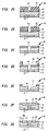
- FIGS. 1A to 1H there are shown eight stages of fabrication of a PRIOR ART semiconductor device or microchip 20 having variously a wafer substrate 21, a first level conductive layer 22, an IMD (intermetal dielectric) insulation layer 23, an insulation layer polished top surface 23a, a first organic ARC (antireflective coating) layer 24, a first photoresist layer 25, e.g., of positive photoresist material, a contact hole (aperture) 26, a deepened and widened contact hole 26a, a via (aperture) 27, a second organic ARC layer 28, a second photoresist layer 29, e.g., of positive photoresist material, an interconnect trench 30, a widened trench 30a, a via trench 31, fences 22, a second level conductive layer 33, and a second level conductive layer polished top surface 33a.
- a first photoresist layer e.g., of positive photoresist material
- a contact hole (aperture) 26a a deepened
- FIGS. 1A to 1H illustrate a typical PRIOR ART method sequence of steps for forming a patterned conductive multilayer arrangement on a semiconductor substrate, which involves a dual damascene metallization scheme using a conventional organic ARC.
- FIG. 1A shows semiconductor device or microchip 20 having a wafer substrate 21, e.g., of silicon, on which a first level conductive layer 22, e.g., of a metal such as tungsten, has been deposited in a selective region thereon, and in turn an IMD insulation layer 23, e.g., of silicon dioxide, a first organic ARC layer 24, and a first photoresist layer 25, e.g., of positive photoresist material. This is followed by patterning (photolithographic exposure and development) to open contact hole 26 to expose the underlying pattern area of first organic ARC layer 24.
- a wafer substrate 21 e.g., of silicon
- a first level conductive layer 22 e.g., of a metal such as tungsten
- FIG. 1B shows semiconductor device 20 after open etching of organic ARC layer 24, which provides a deepened, yet widened, contact hole 26a through organic ARC layer 24 to expose the underlying pattern area of insulation layer 23.
- Contact hole 26a is widened relative to contact hole 26 due to the non-selectivity of the ARC open etch process. This is the condition of semiconductor device 20 after the step (2) of open etching of the first organic ARC layer to deepen the aperture and expose the underlying insulation layer, whereby the aperture pattern is widened due to etching non-selectivity.
- FIG. 1C shows semiconductor device 20 after etching of insulation layer 23, using photoresist layer 25 as a mask, which deepens widened aperture 26a to provide via 27 in insulation layer 23 to expose the underlying region of first level conductive layer 22. This is followed by stripping of photoresist layer 25 and organic ARC layer 24. This is the condition of semiconductor device 20 after the combination step (3) of etching the insulation layer, using the photoresist layer as a mask, to deepen the widened aperture and form a via exposing the underlying first level conductive layer, and then stripping the photoresist layer and organic ARC layer.
- FIG. 1D shows semiconductor device 20 after applying second organic ARC layer 28 on insulation layer 23, which causes via 27 to be filled up with residual organic ARC layer material, and in turn applying second photoresist layer 29, e.g., of positive photoresist material, on organic ARC layer 28. This is followed by patterning (photolithographic exposure and development) of photoresist layer 29 to open interconnect trench 30 therein which surrounds via 27.
- This is the condition of semiconductor device 20 after the combination step (4) of depositing a second organic ARC layer on the insulation layer, whereby the via becomes filled with residual organic ARC material, and depositing a second photoresist layer on the organic ARC layer, followed by patterning to open an interconnect trench in the photoresist layer surrounding the via.
- FIG. 1E shows semiconductor device 20 after open etching of organic ARC layer 28, which provides a deepened, yet widened, trench 30a through organic ARC layer 28 to expose the underlying pattern area of insulation layer 23.
- Trench 30a is widened relative to trench 30 due to the non-selectivity of the organic ARC etch process.
- the body of residual organic ARC material in via 27 is recessed but not completely removed by the organic ARC etch process.
- FIG. 1F shows semiconductor device 20 after etching insulation layer 23 to a desired depth to form via trench 31 which extends the pattern of trench 30a into the upper portion of insulation layer 23, followed by stripping of photoresist layer 29 and organic ARC layer 28. Because of the presence of residual organic ARC material in via 27, fences 32 are left in insulation layer 23 at the center portion of via trench 31 which surrounds via 27. This is the condition of semiconductor device 20 after the combination step (6) of etching the insulation layer to deepen the organic ARC layer trench further and form a corresponding trench in the insulation layer, which leaves fences surrounding the via because of the interfering presence of residual organic ARC material in the via, and then stripping the photoresist layer and organic ARC layer,
- FIG. 1G shows semiconductor device 20 after wet cleaning insulation layer 23, followed by deposition of second level conductive layer 33, e.g., of a metal such as aluminum, on insulation layer 23 which overfills via trench 31 created therein and forms a conductive contact with first level conductive layer 22.
- second level conductive layer 33 e.g., of a metal such as aluminum
- FIG. 1H shows semiconductor device 20 after chemical mechanical polishing (CMP) of surplus second level conductive material from second level conductive layer 33 back down to the level of insulation layer 23 to form polished top surface 23a on insulation layer 23 and polished top surface 33a on second level conductive layer 33 in flush relation to each other, e.g., with some overpolishing at such top surfaces.
- CMP chemical mechanical polishing
- the steps of providing first level conductive layer 22 on wafer substrate 21, depositing insulation layer 23 on wafer substrate 21, applying organic ARC layer 24 on insulation layer 23, applying photoresist layer 25 on organic ARC layer 24, patterning photoresist layer 25, etching organic ARC layer 24, and etching insulation layer 23, are effected by conventional technique.
- the corresponding fabrication technique for forming a patterned conductive multilayer arrangement on a semiconductor substrate which involves a dual damascene metallization scheme using a DARC silicon oxynitride/SOG system, contemplates the following analogous steps:
- FIGS. 2A to 2G there are shown seven stages of fabrication of a semiconductor device or microchip 40 according to an embodiment of the invention, having variously a wafer substrate 21', a first level conductive layer 22', an IMD (intermetal dielectric) insulation layer 23', a DARC (dielectric antireflective coating) silicon oxynitride layer 41, a DARC silicon oxynitride layer polished top surface 41a, an essentially reactive nitrogenous substance-free dielectric spacer layer 42, a first photoresist layer 25', e.g., of positive photoresist material, a contact hole (aperture) 43, a deepened contact hole 43a, a via (aperture) 44, a second photoresist layer 45, e.g., of positive photoresist material, an interconnect trench 46, a via trench 47, a second level conductive layer 48, and a second level conductive layer polished top surface 48a.
- a first photoresist layer 25' e
- FIGS. 2A to 2G parts designated by prime (') numbers are the same as those in FIGS. 1A to 1H.
- FIGS. 2A to 2G illustrate a method sequence of steps for forming a patterned conductive multilayer arrangement on a semiconductor substrate, using silicon oxynitride as a DARC layer and an essentially reactive nitrogenous substance-free dielectric spacer layer between the DARC silicon oxynitride layer and an overlying photoresist layer.
- FIG. 2A shows semiconductor device or microchip 40 having a wafer substrate 21', e.g., of silicon, on which a first level conductive layer 22', e.g., of a metal such as tungsten, has been deposited in a selective region thereon, and in turn an IMD insulation layer 23', e.g., of silicon dioxide, a silicon oxynitride layer 41 forming a DARC (dielectric antireflective coating), an essentially reactive nitrogenous substance-free dielectric spacer layer 42 which prevents photoresist poisoning, and a first photoresist layer 25', e.g., of positive photoresist material.
- a wafer substrate 21' e.g., of silicon
- a first level conductive layer 22' e.g., of a metal such as tungsten
- IMD insulation layer 23' e.g., of silicon dioxide
- a silicon oxynitride layer 41 forming a DARC (dielectric antireflect
- insulation layer 23' may be reduced to compensate for the inclusion of DARC silicon oxynitride layer 41 and dielectric spacer layer 42 in the layer stack.
- FIG. 2B shows semiconductor device 40 after etching dielectric spacer layer 42 and DARC silicon oxynitride layer 41, which provides a deepened, yet unwidened, contact hole 43a through dielectric spacer layer 42 and DARC silicon oxynitride layer 41 to expose the underlying pattern area of insulation layer 23'.
- Contact hole 43a is not widened relative to contact hole 43 due to the selectivity of the dielectric etch process involved. This is the condition of semiconductor device 40 after the step [6] of removing the uncovered pattern portions of the dielectric spacer layer and corresponding underlying portions of the DARC silicon oxynitride layer to uncover corresponding portions of the insulation layer.
- FIG. 2C shows semiconductor device 40 after dielectric etching of insulation layer 23', using dielectric spacer layer 42 as a mask, which deepens unwidened contact hole 43a to provide via 44 in insulation layer 23' for exposing the underlying region of first level conductive layer 22'. This is followed by stripping of photoresist layer 25'.
- the etching operation to form via 44 is advantageously performed within the same chamber zone as the etching operation used to form deepened contact hole 43a, i.e. wafer substrate 21' remains in the same etch chamber for a tandem pair of etching operations. This is the condition of semiconductor device 40 after the steps [7] to [8] of removing the uncovered portions of the insulation layer to uncover the region of the first conductive layer in the substrate, and then stripping the photoresist layer to expose the dielectric spacer layer.
- FIG. 2D shows semiconductor device 40 after applying second photoresist layer 45, e.g., of positive photoresist material, on dielectric spacer layer 42, and patterning (photolithographic exposure and development) of photoresist layer 45 to open interconnect trench 46 therein which surrounds via 44.
- second photoresist layer 45 e.g., of positive photoresist material
- patterning photolithographic exposure and development
- photoresist layer 45 to open interconnect trench 46 therein which surrounds via 44.
- via 44 may initially be partially filled with residual photoresist layer 45 material (not shown), this is removed during the development process for opening trench 46.
- FIG. 2E shows semiconductor device 40 after further dielectric etching of dielectric spacer layer 42, DARC silicon oxynitride layer 41 and the upper course portions of inorganic layer 23' to provide a deepened, yet unwidened, via trench 47 through dielectric spacer layer 42, DARC silicon oxynitride layer 41 and the upper course portions of insulation layer 23' to a desired depth therein. This is followed by stripping of photoresist layer 45. Trench 47 is not widened relative to trench 46 due to the selectivity of the dielectric etch process. Also, no fences are formed in insulation layer 23'.
- FIG. 2F shows semiconductor device 40 after wet cleaning insulation layer 23', followed by deposition of second level conductive layer 48, e.g., of a metal such as aluminum, on insulation layer 23' which overfills via trench 47 created therein and forms a conductive contact with first level conductive layer 22'.
- the wet cleaning operation may also remove the dielectric spacer layer 42.
- the nature of dielectric spacer layer 42, especially where composed of SOG material is such that it generally etches much faster, e.g., in dilute or buffered HF, than commonly denser silicon dioxide in general and silicon oxynitride. This is the condition of semiconductor device 40 after the step [12] of providing a second conductive layer on the widened pattern portions of the insulation layer and in conductive contact with the previously uncovered pattern portions of the first conductive layer region.
- FIG. 2G shows semiconductor device 40 after chemical mechanical polishing (CMP) of surplus second level conductive material from second level conductive layer 48 back down to the level of DARC silicon oxynitride layer 41.
- CMP chemical mechanical polishing
- these layers may be partially or fully removed by the pertinent wet cleaning and CMP operations.
- the steps of providing first level conductive layer 22' on wafer substrate 21', depositing insulation layer 23' on wafer substrate 21', depositing DARC silicon oxynitride layer 41 on insulation layer 23', depositing dielectric spacer layer 42 on DARC silicon oxynitride layer 41, applying photoresist layer 25' on dielectric spacer layer 42, patterning photoresist layer 25', etching dielectric spacer layer 42 and DARC silicon oxynitride layer 41, and etching insulation layer 23', are effected by conventional technique.
- wafer substrate 21' may be made of silicon or another material such as a metal.
- First level conductive layer 22' may be made of, e.g., tungsten and second level conductive layer 48 of, e.g., aluminum.
- Insulation layer 23' may be made of, e.g., silicon dioxide. It serves as an insulation barrier for first level conductive layer 22'.
- insulation layer 23' is provided in a thickness of about 5,000-10,000 angstroms
- DARC silicon oxynitride layer 41 is provided in a thickness of about 300-1,500 angstroms
- dielectric spacer layer 42 is provided in a thickness of about 250-1,000 angstroms.
- DARC silicon oxynitride layer 41 The thickness of DARC silicon oxynitride layer 41 is chosen for it to function either in the destructive interference or absorption mode.
- the photoresist layers are exposed to UV wave irradiation such as at a wavelength of about 193 to 365 nm.
- the above scheme according to the invention which uses an essentially reactive nitrogenous substance-free dielectric spacer layer between a DARC silicon oxynitride layer and a photoresist layer affords better lateral control for the etching operations and provides a thin barrier or shield layer for physically and functionally separating the DARC silicon oxynitride layer from the photoresist layer.
- This separation inhibits reactive nitrogenous substance transport from the DARC silicon oxynitride layer therethrough so as to prevent such reactive nitrogenous substances from reaching and poisoning the photoresist layer to cause footing or pinching formation.
- the dielectric spacer layer is desirably transparent so that the incident light will travel readily therethrough during photoresist exposure for maximum absorption by the DARC silicon oxynitride layer.
- DARC silicon oxynitride layer 41 with dielectric spacer layer 42 is that the DARC silicon oxynitride layer 41 / dielectric spacer layer 42 combination stack can serve to provide a hard mask for subsequent processing.
- a very thin photoresist layer 25' with excellent spacial resolution can be employed to provide selective patterning of dielectric spacer layer 42, followed by stripping of photoresist layer 25', and selective patterning of DARC silicon oxynitride layer 41 using dielectric spacer layer 42 as a hard mask.
- conductive layers 22' and 48, insulation layer 23' and DARC silicon oxynitride layer 41 are typically provided by PECVD technique.
- dielectric spacer layer 42 may be provided by any appropriate technique, including physical or chemical vapor deposition (PVD or CVD), so long as it is formed as a material essentially free from reactive contaminating nitrogenous substances, it is conveniently provided by spin-on technique, e.g., as spin-on glass (SOG), in similar manner to the applying of photoresist layers 25' and 45.
- spin-on technique e.g., as spin-on glass (SOG), in similar manner to the applying of photoresist layers 25' and 45.
- SOG such as the Dow Corning Co.
- Commercial product "Flowable Oxide” lends itself to integration into existing manufacturing processing schemes and is desirably used according to the invention.
- Preferred SOG materials include those based on hydrogen silsesquioxane, other siloxanes, and the like, which are baked to remove the solvent and provide the desired glass.
- SOG is readily fabricated from Si-O containing precursors in solution, being typically dissolved in an organic solvent.
- the SOG solution is spin-deposited in equipment similar to tools (tracks) commonly used to apply organic materials such as photoresist and organic ARC materials.
- the final SOG thickness can be easily controlled via the spin speed and the Si-O based resin solid content. SOG films of excellent uniformity can be deposited at thicknesses of about 250-1,000 angstroms.
- SOG materials generally have enhanced wet etch ratios (e.g., >10x) compared to PECVD oxides, due to the reduced mechanical density of SOG as compared to such oxides, e.g., silicon dioxide.
- the SOG solution also undergoes a series of baking steps (drying bakes) to evaporate the solvent and form the desired Si-O network.
- the temperature for the SOG bakes is typically about 200-350°C, preferably about 250°C.
- the SOG solution is deposited by spin-on technique at room temperature, then baked initially at about 150°C, and finally at about 250°C, all under inert, i.e., non-reactive, nitrogen, to provide a solid oxide (silicon dioxide based) film which forms dielectric spacer layer 42.
- This temperature is higher than that of photoresist bakes, but lower than that of plasma deposition processes.
- photoresist layers 25' and 45 are typically deposited by spin-on deposition and then baked at 90-150°C.
- metals for layers 22' and 48a are deposited at a temperature of up to about 450°C (per CVD or PVD technique), and dielectrics such as silicon dioxide for layer 23' and DARC silicon oxynitride for layer 41 are deposited at a temperature of about 250-400°C, especially about 350°C (per PECVD technique).
- the solid oxide film of SOG produced by baking the spin-on deposited solution is of lower density (and thus more porous) than silicon dioxide deposited by PECVD technique, the freedom from reactive nitrogenous substance contamination of the SOG material in the dielectric spacer layer 42 is what serves to prevent transport of reactive nitrogenous substances from DARC silicon oxynitride layer 41 therethrough to reach photoresist layer 25' or 45, as the case may be.
- the lower density and more porous nature of the SOG material it serves as a sufficient physical and functional spacing structure to keep DARC silicon oxynitride layer 41 and its contents away from the interface with photoresist layer 25' or 45.
- Reactive mobile nitrogen and nitrogen-containing constituents present in DARC silicon oxynitride layer 41 will migrate therefrom into dielectric spacer layer 42.
- any such reactive contaminating nitrogenous substances traceable to DARC silicon oxynitride layer 41 may be retained in or contained by dielectric spacer layer 42 sufficiently to prevent photoresist poisoning during the time that dielectric spacer layer 42 and photoresist layers 25' and 45, all of which are sacrificial layers, remain in the stack (see FIGS. 2A-2E).
- the DARC silicon oxynitride layer is deposited, e.g., by PECVD, on the wafer substrate to be patterned, and a silicon dioxide cap layer for avoiding direct transport of reactive nitrogenous substances from the DARC silicon oxynitride layer to the overlying photoresist layer, is deposited, e.g., by PECVD, on the DARC silicon oxynitride layer.
- a silicon dioxide cap layer for avoiding direct transport of reactive nitrogenous substances from the DARC silicon oxynitride layer to the overlying photoresist layer.
- reactive nitrogenous substances that lead to photoresist poisoning and footing problems are inherently present in the DARC silicon oxynitride layer, and usually also in the silicon dioxide cap layer. They are traceable to reactive nitrogenous constituents in the, e.g., PECVD type, deposition process materials such as silane, oxygen, nitrogen, nitrous oxide, etc., the silane contributing hydrogen during formation of, for example, silicon dioxide or silicon oxynitride.
- both the dielectric spacer layer and photoresist layer can be applied in an integrated manner in tandem steps by spin-on technique, in a different kind of operation.
- the dielectric spacer layer as formed by SOG technique can be versatilely provided in a wide range of thicknesses, and can be applied on tools (tracks) corresponding to those being used in industry for applying deep UV photoresist layers.
- dielectric spacer layer 42 and photoresist layer 25' can be deposited, e.g., by spin-on technique, in sequence onto wafer substrate 21', i.e., onto DARC silicon oxynitride layer 41, in the same deposition zone (track).
- the SOG deposition of dielectric spacer layer 42 can be effected in inert, i.e., non-reactive, nitrogen, with the use of mild thermal baking of the SOG at temperatures akin to those for applying the photoresist layer. These temperatures are much lower than those for plasma deposition of a silicon dioxide cap layer, and the mild conditions do not result in adverse incorporation of the inert nitrogen into the SOG.
- Another advantage of the invention is that, after the pertinent photolithographic operation, the SOG of dielectric spacer layer 42 can be easily stripped in a dual damascene application, e.g., by combining the SOG strip with a buffered HF pre-cleaning step, e.g., prior to a second level metal deposition step.
- both the SOG and photoresist layers can be deposited in sequence in the same deposition zone (track).
- DARC silicon oxynitride layer 41 achieves desired uniform reflectance control for contact photolithographic processing since it is an excellent antireflective material for both MUV (typically of 365 nm wavelength) and DUV (typically of 248 nm or less) photolithographic processing.
- the silicon oxynitride composition can be adjusted to optimize its antireflective property by suitably changing the composition ratio of the SiO x N y components, where x is 0.5-1.5 and y is 0.1-1.5, i.e., SIO 0.5-1.5 N 0.1-1.5 , for example, per PECVD using silane (SiH 4 ) with nitrous oxide (N 2 O).
- U.S. Patent No. 5,219,788 discloses a metal nitride ARC layer of TiN on a metal conductive bilayer on a substrate, and a silicon-containing barrier layer of sputtered silicon or SiO 2 , or of SOG per said [5] U.S. Patent No. 4,981,530 (Clodgo et al.), on the TiN ARC layer.
- the barrier layer is needed to separate the TiN ARC layer from a photoresist layer that generates acid groups on exposure per said [2] U.S. Patent No. 4,491,628 (Ito et al.), to reduce the resist poisoning effect called "webbing" caused by the TiN ARC layer.
- the dielectric spacer layer 42 in order to perform its physical and functional nitrogenous substance flow-inhibiting effect, the dielectric spacer layer 42 must be free from contaminating reactive nitrogenous substances per se and also those specifically traceable to silicon oxynitride (rather than to TiN) as a DARC material that can potentially poison the photoresist material.
- the dielectric spacer layer 42 is also free from dye as contemplated by said [3] U.S. Patent No. 4,587,138 (Yau et al.), issued May 6, 1986, i.e., that nullifies the transparency of the SOG material and causes it to function as an ARC layer.
- the silicon oxynitride used as the ARC material per DARC silicon oxynitride layer 41 is a true dielectric ARC material which is not restricted to the patterning of metal conductive layers but rather is usable for patterning various other types of layer materials as well.
Abstract
Description
Claims (17)
- A method of forming a patterned conductive multilayer arrangement on a semiconductor substrate comprising the steps of:providing a dielectric insulation layer on a surface of a semiconductor substrate having a first conductive layer disposed in a selective region thereon such that the insulation layer overlies the region of the first conductive layer;providing a silicon oxynitride layer on the insulating layer sufficiently to form a dielectric antireflective coating thereon;providing an essentially reactive nitrogenous substance-free dielectric spacer layer on the antireflective coating silicon oxynitride layer sufficiently to prevent reactive nitrogenous substance transport therethrough from the silicon oxynitride layer;providing a photoresist layer on the dielectric spacer layer;selectively exposing and developing the photoresist layer to uncover selective pattern portions of the underlying dielectric spacer layer, which pattern portions are in overlying aligned relation to the first conductive layer region in the substrate;removing the uncovered pattern portions of the dielectric spacer layer and corresponding underlying portions of the silicon oxynitride layer for uncovering corresponding portions of the underlying insulation layer; andremoving the uncovered portions of the insulation layer to uncover the region of the first conductive layer in the substrate.
- The method of claim 1 wherein the insulation layer is formed of silicon dioxide, and the first conductive layer is formed of metal.
- The method of claim 1 wherein the dielectric spacer layer is formed of essentially reactive nitrogenous substance-free silicon dioxide material, and the photoresist layer is formed of an organic photoresist material susceptible to reactive nitrogenous substance poisoning.
- The method of claim 3 wherein the dielectric spacer layer is formed of essentially reactive nitrogenous substance-free spin-on glass.
- The method of claim 1 wherein the uncovered pattern portions of the dielectric spacer layer and corresponding underlying portions of the silicon oxynitride layer are removed together in a first etching step in a chamber zone, and the uncovered portions of the insulation layer are removed in a second etching step immediately following the first etching step in the same chamber zone.
- The method of claim 5 wherein the first etching step and second etching step are dry etching steps.
- The method of claim 1 further including the steps of:removing the remainder of the developed photoresist layer to expose the dielectric spacer layer;providing a further photoresist layer on the dielectric spacer layer and in surrounding relation to the previously removed pattern portions of the dielectric spacer layer;selectively exposing and developing the further photoresist layer to uncover widened pattern portions surrounding the previously removed pattern portions of the dielectric spacer layer;removing the uncovered widened pattern portions of the dielectric spacer layer and corresponding underlying portions of the silicon oxynitride layer and upper course portions of the underlying widened portions of the insulation layer surrounding the previously uncovered first conductive layer region; andproviding a second conductive layer on the widened pattern portions of the insulation layer and in conductive contact with the previously uncovered pattern portions of the first conductive layer region.
- The method of claim 7 wherein the insulation layer is formed of silicon dioxide, and the first and second conductive layers are respectively formed of metal.
- The method of claim 7 wherein the dielectric spacer layer is formed of essentially reactive nitrogenous substance-free silicon dioxide material, and the photoresist layer is formed of an organic photoresist material susceptible to reactive nitrogenous substance poisoning.
- The method of claim 9 wherein the dielectric spacer layer is formed of essentially reactive nitrogenous substance-free spin-on glass.
- The method of claim 1 wherein the insulation layer is provided in a thickness of about 5,000-10,000 angstroms, the silicon oxynitride layer is provided in a thickness of about 300-1,500 angstroms, and the dielectric spacer layer is provided in a thickness of about 250-1,000 angstroms.
- The method of claim 1 wherein the dielectric spacer layer and the photoresist layer are provided by deposition in sequence onto the antireflective silicon oxynitride layer in the same deposition zone.
- A method of treating a wafer substrate in semiconductor fabrication for inhibiting reactive nitrogenous substance flow from a silicon oxynitride layer forming a dielectric antireflective coating thereon to an overlying photoresist layer to prevent reactive nitrogenous substance poisoning of the photoresist layer, which comprises interposing an essentially reactive nitrogenous substance-free dielectric spacer layer between the silicon oxynitride layer and the overlying photoresist layer sufficiently to prevent reactive nitrogenous substance transport therethrough from the dielectric antireflective coating silicon oxynitride layer to the photoresist layer.
- The method of claim 13 wherein the dielectric spacer layer is formed of essentially reactive nitrogenous substance-free silicon dioxide material, and the photoresist layer is formed of an organic photoresist material susceptible to reactive nitrogenous substance poisoning.
- The method of claim 14 wherein the dielectric spacer layer is formed of essentially reactive nitrogenous substance-free spin-on glass.
- The method of claim 13 wherein the dielectric spacer layer and the photoresist layer are provided by deposition in sequence onto the antireflective silicon oxynitride layer in the same deposition zone.
- The product formed by the method of claim 13.
Applications Claiming Priority (2)
| Application Number | Priority Date | Filing Date | Title |
|---|---|---|---|
| US09/120,629 US6103456A (en) | 1998-07-22 | 1998-07-22 | Prevention of photoresist poisoning from dielectric antireflective coating in semiconductor fabrication |
| US120629 | 1998-07-22 |
Publications (1)
| Publication Number | Publication Date |
|---|---|
| EP0975010A1 true EP0975010A1 (en) | 2000-01-26 |
Family
ID=22391561
Family Applications (1)
| Application Number | Title | Priority Date | Filing Date |
|---|---|---|---|
| EP99113532A Withdrawn EP0975010A1 (en) | 1998-07-22 | 1999-07-06 | Prevention of photoresist poisoning from dielectric antireflective coating in semiconductor fabrication |
Country Status (6)
| Country | Link |
|---|---|
| US (1) | US6103456A (en) |
| EP (1) | EP0975010A1 (en) |
| JP (1) | JP2000068268A (en) |
| KR (1) | KR20000016960A (en) |
| CN (1) | CN1256438A (en) |
| TW (1) | TW436967B (en) |
Cited By (10)
| Publication number | Priority date | Publication date | Assignee | Title |
|---|---|---|---|---|
| DE10030444A1 (en) * | 2000-06-22 | 2002-01-10 | Infineon Technologies Ag | Process for the production of a dielectric antifuse structure |
| EP1180554A2 (en) * | 2000-08-12 | 2002-02-20 | Applied Materials, Inc. | Method of depositing organosilicate layers |
| EP1191123A2 (en) * | 2000-09-12 | 2002-03-27 | Applied Materials, Inc. | Dual frequency plasma enhanced chemical vapor deposition of silicon carbide layers |
| EP1280197A1 (en) * | 2001-07-09 | 2003-01-29 | Texas Instruments Incorporated | Process for forming a dual damascene structure |
| GB2386755A (en) * | 2002-01-02 | 2003-09-24 | Agere Systems Inc | Isolating porous low-k dielectrics |
| WO2004003998A1 (en) * | 2002-06-28 | 2004-01-08 | Infineon Technologies Ag | Method for contacting parts of a component integrated into a semiconductor substrate |
| WO2004061949A1 (en) * | 2002-12-23 | 2004-07-22 | Advanced Micro Devices, Inc. | Method of forming a cap layer having anti-reflective characteristics on top of a low-k dielectric |
| WO2004084290A1 (en) * | 2003-03-17 | 2004-09-30 | Applied Materials Inc. | A nitrogen-free hard mask over low k dielectric |
| US7030044B2 (en) | 2002-12-23 | 2006-04-18 | Advanced Micro Devices, Inc. | Method of forming a cap layer having anti-reflective characteristics on top of a low-k dielectric |
| DE10062660B4 (en) * | 2000-12-15 | 2010-05-06 | Advanced Micro Devices, Inc., Sunnyvale | A method of making a silicon oxynitride ARC layer over a semiconductor structure |
Families Citing this family (92)
| Publication number | Priority date | Publication date | Assignee | Title |
|---|---|---|---|---|
| US6121133A (en) | 1997-08-22 | 2000-09-19 | Micron Technology, Inc. | Isolation using an antireflective coating |
| US6355196B1 (en) * | 1998-03-16 | 2002-03-12 | Vantico Inc. | Process for producing direct tooling mold and method for using the same |
| US6300672B1 (en) * | 1998-07-22 | 2001-10-09 | Siemens Aktiengesellschaft | Silicon oxynitride cap for fluorinated silicate glass film in intermetal dielectric semiconductor fabrication |
| US6294459B1 (en) | 1998-09-03 | 2001-09-25 | Micron Technology, Inc. | Anti-reflective coatings and methods for forming and using same |
| US6974766B1 (en) | 1998-10-01 | 2005-12-13 | Applied Materials, Inc. | In situ deposition of a low κ dielectric layer, barrier layer, etch stop, and anti-reflective coating for damascene application |
| US6635583B2 (en) | 1998-10-01 | 2003-10-21 | Applied Materials, Inc. | Silicon carbide deposition for use as a low-dielectric constant anti-reflective coating |
| US6165855A (en) * | 1998-12-04 | 2000-12-26 | Advanced Micro Devices, Inc. | Antireflective coating used in the fabrication of microcircuit structures in 0.18 micron and smaller technologies |
| JP3257533B2 (en) * | 1999-01-25 | 2002-02-18 | 日本電気株式会社 | Wiring formation method using inorganic anti-reflection film |
| KR100280288B1 (en) * | 1999-02-04 | 2001-01-15 | 윤종용 | Method for fabricating capacitor of semiconcuctor integrated circuit |
| US6713234B2 (en) * | 1999-02-18 | 2004-03-30 | Micron Technology, Inc. | Fabrication of semiconductor devices using anti-reflective coatings |
| US6245629B1 (en) * | 1999-03-25 | 2001-06-12 | Infineon Technologies North America Corp. | Semiconductor structures and manufacturing methods |
| US6444588B1 (en) | 1999-04-26 | 2002-09-03 | Micron Technology, Inc. | Anti-reflective coatings and methods regarding same |
| US6461955B1 (en) * | 1999-04-29 | 2002-10-08 | Texas Instruments Incorporated | Yield improvement of dual damascene fabrication through oxide filling |
| US7045454B1 (en) | 1999-05-11 | 2006-05-16 | Micron Technology, Inc. | Chemical mechanical planarization of conductive material |
| CA2374944A1 (en) | 1999-06-10 | 2000-12-21 | Nigel Hacker | Spin-on-glass anti-reflective coatings for photolithography |
| US6824879B2 (en) | 1999-06-10 | 2004-11-30 | Honeywell International Inc. | Spin-on-glass anti-reflective coatings for photolithography |
| US20040034134A1 (en) * | 1999-08-26 | 2004-02-19 | Lamb James E. | Crosslinkable fill compositions for uniformly protecting via and contact holes |
| JP5079959B2 (en) * | 1999-08-26 | 2012-11-21 | ブルーワー サイエンス アイ エヌ シー. | Improved packing material for dual damascene process |
| US20050158666A1 (en) * | 1999-10-15 | 2005-07-21 | Taiwan Semiconductor Manufacturing Company, Ltd. | Lateral etch inhibited multiple etch method for etching material etchable with oxygen containing plasma |
| US6245656B1 (en) * | 1999-11-08 | 2001-06-12 | Vanguard International Semiconductor Corporation | Method for producing multi-level contacts |
| US6197681B1 (en) * | 1999-12-31 | 2001-03-06 | United Microelectronics Corp. | Forming copper interconnects in dielectric materials with low constant dielectrics |
| US6995068B1 (en) | 2000-06-09 | 2006-02-07 | Newport Fab, Llc | Double-implant high performance varactor and method for manufacturing same |
| TWI293044B (en) * | 2000-06-21 | 2008-02-01 | Dainippon Printing Co Ltd | |
| US6271128B1 (en) * | 2000-09-29 | 2001-08-07 | Vanguard International Semiconductor Corp. | Method for fabricating transistor |
| US6355556B1 (en) * | 2000-09-29 | 2002-03-12 | Vanguard International Semiconductor Corp. | Method for fabricating transistor |
| US6962771B1 (en) * | 2000-10-13 | 2005-11-08 | Taiwan Semiconductor Manufacturing Company, Ltd. | Dual damascene process |
| US6455416B1 (en) * | 2000-10-24 | 2002-09-24 | Advanced Micro Devices, Inc. | Developer soluble dyed BARC for dual damascene process |
| US7132219B2 (en) * | 2001-02-02 | 2006-11-07 | Brewer Science Inc. | Polymeric antireflective coatings deposited by plasma enhanced chemical vapor deposition |
| US6537733B2 (en) * | 2001-02-23 | 2003-03-25 | Applied Materials, Inc. | Method of depositing low dielectric constant silicon carbide layers |
| US6458508B1 (en) * | 2001-02-23 | 2002-10-01 | Lsi Logic Corporation | Method of protecting acid-catalyzed photoresist from chip-generated basic contaminants |
| US6537908B2 (en) * | 2001-02-28 | 2003-03-25 | International Business Machines Corporation | Method for dual-damascence patterning of low-k interconnects using spin-on distributed hardmask |
| US6472333B2 (en) | 2001-03-28 | 2002-10-29 | Applied Materials, Inc. | Silicon carbide cap layers for low dielectric constant silicon oxide layers |
| US6458691B1 (en) | 2001-04-04 | 2002-10-01 | Advanced Micro Devices, Inc. | Dual inlaid process using an imaging layer to protect via from poisoning |
| US6589711B1 (en) | 2001-04-04 | 2003-07-08 | Advanced Micro Devices, Inc. | Dual inlaid process using a bilayer resist |
| US7125783B2 (en) * | 2001-04-18 | 2006-10-24 | Integrated Device Technology, Inc. | Dielectric anti-reflective coating surface treatment to prevent defect generation in associated wet clean |
| US6410424B1 (en) * | 2001-04-19 | 2002-06-25 | Taiwan Semiconductor Manufacturing Company | Process flow to optimize profile of ultra small size photo resist free contact |
| US6893684B2 (en) * | 2001-06-05 | 2005-05-17 | Brewer Science Inc. | Anti-reflective coating compositions for use with low k dielectric materials |
| US6670425B2 (en) | 2001-06-05 | 2003-12-30 | Brewer Science, Inc. | Anti-reflective coating of polymer with epoxide rings reacted with light attenuating compound and unreacted epoxide rings |
| US6391757B1 (en) * | 2001-06-06 | 2002-05-21 | United Microelectronics Corp. | Dual damascene process |
| US6846749B1 (en) | 2001-06-25 | 2005-01-25 | Advanced Micro Devices, Inc. | N-containing plasma etch process with reduced resist poisoning |
| US6534397B1 (en) * | 2001-07-13 | 2003-03-18 | Advanced Micro Devices, Inc. | Pre-treatment of low-k dielectric for prevention of photoresist poisoning |
| US6583046B1 (en) | 2001-07-13 | 2003-06-24 | Advanced Micro Devices, Inc. | Post-treatment of low-k dielectric for prevention of photoresist poisoning |
| US20030037960A1 (en) * | 2001-08-27 | 2003-02-27 | Ohr Stephen S. | Layered circuit boards and methods of production thereof |
| US6656837B2 (en) * | 2001-10-11 | 2003-12-02 | Applied Materials, Inc. | Method of eliminating photoresist poisoning in damascene applications |
| US6790770B2 (en) * | 2001-11-08 | 2004-09-14 | Taiwan Semiconductor Manufacturing Co., Ltd | Method for preventing photoresist poisoning |
| AU2002227106A1 (en) | 2001-11-15 | 2003-06-10 | Honeywell International Inc. | Spin-on anti-reflective coatings for photolithography |
| US6633392B1 (en) | 2002-01-17 | 2003-10-14 | Advanced Micro Devices, Inc. | X-ray reflectance system to determine suitability of SiON ARC layer |
| US6989230B2 (en) * | 2002-03-29 | 2006-01-24 | Infineon Technologies Ag | Producing low k inter-layer dielectric films using Si-containing resists |
| TW527699B (en) * | 2002-04-16 | 2003-04-11 | Macronix Int Co Ltd | Method for manufacturing a semiconductor device |
| US6852474B2 (en) * | 2002-04-30 | 2005-02-08 | Brewer Science Inc. | Polymeric antireflective coatings deposited by plasma enhanced chemical vapor deposition |
| US6949389B2 (en) * | 2002-05-02 | 2005-09-27 | Osram Opto Semiconductors Gmbh | Encapsulation for organic light emitting diodes devices |
| JP2004014841A (en) * | 2002-06-07 | 2004-01-15 | Fujitsu Ltd | Semiconductor device and its manufacturing method |
| US6764749B2 (en) * | 2002-07-29 | 2004-07-20 | Lsi Logic Corporation | Method to improve the resolution of a photolithography system by use of a coupling layer between the photo resist and the ARC |
| US7887875B2 (en) * | 2002-09-30 | 2011-02-15 | Texas Instruments Incorporated | Method to reduce photoresist poisoning |
| US7109119B2 (en) * | 2002-10-31 | 2006-09-19 | Taiwan Semiconductor Manufacturing Company, Ltd. | Scum solution for chemically amplified resist patterning in cu/low k dual damascene |
| US6853043B2 (en) * | 2002-11-04 | 2005-02-08 | Applied Materials, Inc. | Nitrogen-free antireflective coating for use with photolithographic patterning |
| US7153776B2 (en) * | 2002-11-27 | 2006-12-26 | International Business Machines Corporation | Method for reducing amine based contaminants |
| US7018779B2 (en) * | 2003-01-07 | 2006-03-28 | International Business Machines Corporation | Apparatus and method to improve resist line roughness in semiconductor wafer processing |
| US7109101B1 (en) * | 2003-05-06 | 2006-09-19 | Amd, Inc. | Capping layer for reducing amorphous carbon contamination of photoresist in semiconductor device manufacture; and process for making same |
| US7015136B2 (en) * | 2003-07-10 | 2006-03-21 | Taiwan Semiconductor Manufacturing Co., Ltd. | Method for preventing formation of photoresist scum |
| US8053159B2 (en) | 2003-11-18 | 2011-11-08 | Honeywell International Inc. | Antireflective coatings for via fill and photolithography applications and methods of preparation thereof |
| DE10356668B4 (en) * | 2003-12-04 | 2005-11-03 | Infineon Technologies Ag | Manufacturing method for a hard mask on a semiconductor structure |
| US20050170638A1 (en) * | 2004-01-30 | 2005-08-04 | Bang-Ching Ho | Method for forming dual damascene interconnect structure |
| US20050255410A1 (en) | 2004-04-29 | 2005-11-17 | Guerrero Douglas J | Anti-reflective coatings using vinyl ether crosslinkers |
| US7507521B2 (en) * | 2004-08-09 | 2009-03-24 | Intel Corporation | Silicon based optically degraded arc for lithographic patterning |
| JP5122063B2 (en) * | 2004-08-17 | 2013-01-16 | 株式会社オハラ | Lithium ion secondary battery and solid electrolyte |
| US7687225B2 (en) * | 2004-09-29 | 2010-03-30 | Intel Corporation | Optical coatings |
| US7262129B2 (en) * | 2004-11-19 | 2007-08-28 | Texas Instruments Incorporated | Minimizing resist poisoning in the manufacture of semiconductor devices |
| JP4533304B2 (en) * | 2005-11-29 | 2010-09-01 | 富士通セミコンダクター株式会社 | Manufacturing method of semiconductor device |
| US8034722B2 (en) * | 2006-04-07 | 2011-10-11 | Taiwan Semiconductor Manufacturing Co., Ltd. | Method of forming dual damascene semiconductor device |
| US7550377B2 (en) * | 2006-06-22 | 2009-06-23 | United Microelectronics Corp. | Method for fabricating single-damascene structure, dual damascene structure, and opening thereof |
| US7914974B2 (en) | 2006-08-18 | 2011-03-29 | Brewer Science Inc. | Anti-reflective imaging layer for multiple patterning process |
| CN101523292B (en) * | 2006-10-12 | 2013-04-10 | 日产化学工业株式会社 | Method for manufacturing semiconductor device using quadruple-layer laminate |
| US8642246B2 (en) | 2007-02-26 | 2014-02-04 | Honeywell International Inc. | Compositions, coatings and films for tri-layer patterning applications and methods of preparation thereof |
| US20090032491A1 (en) * | 2007-08-03 | 2009-02-05 | International Business Machines Corporation | Conductive element forming using sacrificial layer patterned to form dielectric layer |
| CN101393842B (en) * | 2007-09-20 | 2011-08-17 | 中芯国际集成电路制造(上海)有限公司 | Slot forming method |
| US8003522B2 (en) * | 2007-12-19 | 2011-08-23 | Fairchild Semiconductor Corporation | Method for forming trenches with wide upper portion and narrow lower portion |
| CN101971102B (en) * | 2008-01-29 | 2012-12-12 | 布鲁尔科技公司 | On-track process for patterning hardmask by multiple dark field exposures |
| WO2010073226A2 (en) * | 2008-12-24 | 2010-07-01 | X-Fab Semiconductor Foundries Ag | Production of high alignment marks and such alignment marks on a semiconductor wafer |
| US9640396B2 (en) * | 2009-01-07 | 2017-05-02 | Brewer Science Inc. | Spin-on spacer materials for double- and triple-patterning lithography |
| US8557877B2 (en) | 2009-06-10 | 2013-10-15 | Honeywell International Inc. | Anti-reflective coatings for optically transparent substrates |
| US8864898B2 (en) | 2011-05-31 | 2014-10-21 | Honeywell International Inc. | Coating formulations for optical elements |
| CN104733290B (en) * | 2013-12-19 | 2017-11-24 | 中芯国际集成电路制造(上海)有限公司 | The painting method of bottom antireflective coating |
| EP3194502A4 (en) | 2015-04-13 | 2018-05-16 | Honeywell International Inc. | Polysiloxane formulations and coatings for optoelectronic applications |
| CN105047531B (en) * | 2015-06-07 | 2018-06-29 | 上海华虹宏力半导体制造有限公司 | A kind of reworking method of polyimide coating |
| KR20170042432A (en) * | 2015-10-08 | 2017-04-19 | 삼성전자주식회사 | Method for inspecting photoresist pattern |
| US9917027B2 (en) * | 2015-12-30 | 2018-03-13 | Globalfoundries Singapore Pte. Ltd. | Integrated circuits with aluminum via structures and methods for fabricating the same |
| KR102530534B1 (en) * | 2016-02-17 | 2023-05-09 | 삼성전자주식회사 | Photomask and method for manufacturing semiconductor device using the same |
| US10345702B2 (en) | 2017-08-24 | 2019-07-09 | International Business Machines Corporation | Polymer brushes for extreme ultraviolet photolithography |
| CN109841573A (en) * | 2017-11-28 | 2019-06-04 | 中芯国际集成电路制造(上海)有限公司 | The forming method of semiconductor devices |
| CN112768342B (en) * | 2019-11-02 | 2022-03-22 | 长鑫存储技术有限公司 | Semiconductor structure and forming method thereof |
| US11295978B2 (en) * | 2020-04-29 | 2022-04-05 | International Business Machines Corporation | Interconnects having spacers for improved top via critical dimension and overlay tolerance |
Citations (3)
| Publication number | Priority date | Publication date | Assignee | Title |
|---|---|---|---|---|
| US5219788A (en) * | 1991-02-25 | 1993-06-15 | Ibm Corporation | Bilayer metallization cap for photolithography |
| US5643833A (en) * | 1993-08-31 | 1997-07-01 | Sony Corporation | Method of making a contact hole in a semiconductor device |
| EP0840361A2 (en) * | 1996-11-04 | 1998-05-06 | Applied Materials, Inc. | Method and apparatus for depositing a film over a substrate |
Family Cites Families (9)
| Publication number | Priority date | Publication date | Assignee | Title |
|---|---|---|---|---|
| US3884698A (en) * | 1972-08-23 | 1975-05-20 | Hewlett Packard Co | Method for achieving uniform exposure in a photosensitive material on a semiconductor wafer |
| US4491628A (en) * | 1982-08-23 | 1985-01-01 | International Business Machines Corporation | Positive- and negative-working resist compositions with acid generating photoinitiator and polymer with acid labile groups pendant from polymer backbone |
| US4587138A (en) * | 1984-11-09 | 1986-05-06 | Intel Corporation | MOS rear end processing |
| US4820611A (en) * | 1987-04-24 | 1989-04-11 | Advanced Micro Devices, Inc. | Titanium nitride as an antireflection coating on highly reflective layers for photolithography |
| US4981530A (en) * | 1988-11-28 | 1991-01-01 | International Business Machines Corporation | Planarizing ladder-type silsesquioxane polymer insulation layer |
| KR100366910B1 (en) * | 1994-04-05 | 2003-03-04 | 소니 가부시끼 가이샤 | Manufacturing method of semiconductor device |
| KR960005761A (en) * | 1994-07-27 | 1996-02-23 | 이데이 노부유끼 | Semiconductor device |
| US5643822A (en) * | 1995-01-10 | 1997-07-01 | International Business Machines Corporation | Method for forming trench-isolated FET devices |
| JPH0980755A (en) * | 1995-09-12 | 1997-03-28 | Sony Corp | Resist process and multilayered resist film |
-
1998
- 1998-07-22 US US09/120,629 patent/US6103456A/en not_active Expired - Lifetime
-
1999
- 1999-07-06 EP EP99113532A patent/EP0975010A1/en not_active Withdrawn
- 1999-07-20 TW TW088112285A patent/TW436967B/en not_active IP Right Cessation
- 1999-07-21 KR KR1019990029467A patent/KR20000016960A/en not_active Application Discontinuation
- 1999-07-22 JP JP11207762A patent/JP2000068268A/en not_active Withdrawn
- 1999-07-22 CN CN99110664A patent/CN1256438A/en active Pending
Patent Citations (3)
| Publication number | Priority date | Publication date | Assignee | Title |
|---|---|---|---|---|
| US5219788A (en) * | 1991-02-25 | 1993-06-15 | Ibm Corporation | Bilayer metallization cap for photolithography |
| US5643833A (en) * | 1993-08-31 | 1997-07-01 | Sony Corporation | Method of making a contact hole in a semiconductor device |
| EP0840361A2 (en) * | 1996-11-04 | 1998-05-06 | Applied Materials, Inc. | Method and apparatus for depositing a film over a substrate |
Cited By (17)
| Publication number | Priority date | Publication date | Assignee | Title |
|---|---|---|---|---|
| US6387792B2 (en) | 2000-06-22 | 2002-05-14 | Infineon Technologies Ag | Method of fabricating a dielectric antifuse structure |
| DE10030444A1 (en) * | 2000-06-22 | 2002-01-10 | Infineon Technologies Ag | Process for the production of a dielectric antifuse structure |
| EP1180554A2 (en) * | 2000-08-12 | 2002-02-20 | Applied Materials, Inc. | Method of depositing organosilicate layers |
| EP1180554A3 (en) * | 2000-08-12 | 2005-02-02 | Applied Materials, Inc. | Method of depositing organosilicate layers |
| EP1191123A2 (en) * | 2000-09-12 | 2002-03-27 | Applied Materials, Inc. | Dual frequency plasma enhanced chemical vapor deposition of silicon carbide layers |
| EP1191123A3 (en) * | 2000-09-12 | 2004-11-17 | Applied Materials, Inc. | Dual frequency plasma enhanced chemical vapor deposition of silicon carbide layers |
| DE10062660B4 (en) * | 2000-12-15 | 2010-05-06 | Advanced Micro Devices, Inc., Sunnyvale | A method of making a silicon oxynitride ARC layer over a semiconductor structure |
| US6798043B2 (en) | 2001-06-28 | 2004-09-28 | Agere Systems, Inc. | Structure and method for isolating porous low-k dielectric films |
| EP1280197A1 (en) * | 2001-07-09 | 2003-01-29 | Texas Instruments Incorporated | Process for forming a dual damascene structure |
| US7112532B2 (en) | 2001-07-09 | 2006-09-26 | Texas Instruments Incorporated | Process for forming a dual damascene structure |
| US6605540B2 (en) | 2001-07-09 | 2003-08-12 | Texas Instruments Incorporated | Process for forming a dual damascene structure |
| GB2386755A (en) * | 2002-01-02 | 2003-09-24 | Agere Systems Inc | Isolating porous low-k dielectrics |
| WO2004003998A1 (en) * | 2002-06-28 | 2004-01-08 | Infineon Technologies Ag | Method for contacting parts of a component integrated into a semiconductor substrate |
| US7396749B2 (en) | 2002-06-28 | 2008-07-08 | Infineon Technologies Ag | Method for contacting parts of a component integrated into a semiconductor substrate |
| WO2004061949A1 (en) * | 2002-12-23 | 2004-07-22 | Advanced Micro Devices, Inc. | Method of forming a cap layer having anti-reflective characteristics on top of a low-k dielectric |
| US7030044B2 (en) | 2002-12-23 | 2006-04-18 | Advanced Micro Devices, Inc. | Method of forming a cap layer having anti-reflective characteristics on top of a low-k dielectric |
| WO2004084290A1 (en) * | 2003-03-17 | 2004-09-30 | Applied Materials Inc. | A nitrogen-free hard mask over low k dielectric |
Also Published As
| Publication number | Publication date |
|---|---|
| CN1256438A (en) | 2000-06-14 |
| US6103456A (en) | 2000-08-15 |
| TW436967B (en) | 2001-05-28 |
| KR20000016960A (en) | 2000-03-25 |
| JP2000068268A (en) | 2000-03-03 |
Similar Documents
| Publication | Publication Date | Title |
|---|---|---|
| US6103456A (en) | Prevention of photoresist poisoning from dielectric antireflective coating in semiconductor fabrication | |
| US6300672B1 (en) | Silicon oxynitride cap for fluorinated silicate glass film in intermetal dielectric semiconductor fabrication | |
| US6365529B1 (en) | Method for patterning dual damascene interconnects using a sacrificial light absorbing material | |
| US6465358B1 (en) | Post etch clean sequence for making a semiconductor device | |
| US6448177B1 (en) | Method of making a semiconductor device having a dual damascene interconnect spaced from a support structure | |
| US7256136B2 (en) | Self-patterning of photo-active dielectric materials for interconnect isolation | |
| US6319821B1 (en) | Dual damascene approach for small geometry dimension | |
| US20050191851A1 (en) | Barrier metal cap structure on copper lines and vias | |
| US6448185B1 (en) | Method for making a semiconductor device that has a dual damascene interconnect | |
| US6133137A (en) | Semiconductor device and method of manufacturing the same | |
| US5882999A (en) | Process for metallization of an insulation layer | |
| US20060091431A1 (en) | Contact plug processing and a contact plug | |
| KR20010030302A (en) | Process for fabricating a semiconductor device | |
| US6043146A (en) | Process for forming a semiconductor device | |
| US6946391B2 (en) | Method for forming dual damascenes | |
| US6638853B1 (en) | Method for avoiding photoresist resist residue on semioconductor feature sidewalls | |
| KR960011464B1 (en) | Semiconductor device and manufacturing method thereof | |
| US5283208A (en) | Method of making a submicrometer local structure using an organic mandrel | |
| US20040137709A1 (en) | Metal barrier cap fabrication by polymer lift-off | |
| KR100562540B1 (en) | Deep submicron metallization using deep uv photoresist | |
| US6821896B1 (en) | Method to eliminate via poison effect | |
| US20040175933A1 (en) | Method of forming wiring structure | |
| US6156460A (en) | Photo-mask and method of fabricating the same | |
| US6800548B2 (en) | Method to avoid via poisoning in dual damascene process | |
| US7094683B2 (en) | Dual damascene method for ultra low K dielectrics |
Legal Events
| Date | Code | Title | Description |
|---|---|---|---|
| PUAI | Public reference made under article 153(3) epc to a published international application that has entered the european phase |
Free format text: ORIGINAL CODE: 0009012 |
|
| AK | Designated contracting states |
Kind code of ref document: A1 Designated state(s): DE FR GB IE IT NL |
|
| AX | Request for extension of the european patent |
Free format text: AL;LT;LV;MK;RO;SI |
|
| 17P | Request for examination filed |
Effective date: 20000511 |
|
| AKX | Designation fees paid |
Free format text: DE FR GB IE IT NL |
|
| 17Q | First examination report despatched |
Effective date: 20040702 |
|
| STAA | Information on the status of an ep patent application or granted ep patent |
Free format text: STATUS: THE APPLICATION IS DEEMED TO BE WITHDRAWN |
|
| 18D | Application deemed to be withdrawn |
Effective date: 20050113 |
|
| REG | Reference to a national code |
Ref country code: HK Ref legal event code: WD Ref document number: 1022211 Country of ref document: HK |