EP0997712A2 - Capacitive fluid sensing device and manufacturing method - Google Patents
Capacitive fluid sensing device and manufacturing method Download PDFInfo
- Publication number
- EP0997712A2 EP0997712A2 EP99121294A EP99121294A EP0997712A2 EP 0997712 A2 EP0997712 A2 EP 0997712A2 EP 99121294 A EP99121294 A EP 99121294A EP 99121294 A EP99121294 A EP 99121294A EP 0997712 A2 EP0997712 A2 EP 0997712A2
- Authority
- EP
- European Patent Office
- Prior art keywords
- plates
- carrier
- carrier plates
- capacitor
- sensor arrangement
- Prior art date
- Legal status (The legal status is an assumption and is not a legal conclusion. Google has not performed a legal analysis and makes no representation as to the accuracy of the status listed.)
- Granted
Links
Images


Classifications
-
- G—PHYSICS
- G01—MEASURING; TESTING
- G01F—MEASURING VOLUME, VOLUME FLOW, MASS FLOW OR LIQUID LEVEL; METERING BY VOLUME
- G01F23/00—Indicating or measuring liquid level or level of fluent solid material, e.g. indicating in terms of volume or indicating by means of an alarm
- G01F23/22—Indicating or measuring liquid level or level of fluent solid material, e.g. indicating in terms of volume or indicating by means of an alarm by measuring physical variables, other than linear dimensions, pressure or weight, dependent on the level to be measured, e.g. by difference of heat transfer of steam or water
- G01F23/26—Indicating or measuring liquid level or level of fluent solid material, e.g. indicating in terms of volume or indicating by means of an alarm by measuring physical variables, other than linear dimensions, pressure or weight, dependent on the level to be measured, e.g. by difference of heat transfer of steam or water by measuring variations of capacity or inductance of capacitors or inductors arising from the presence of liquid or fluent solid material in the electric or electromagnetic fields
- G01F23/263—Indicating or measuring liquid level or level of fluent solid material, e.g. indicating in terms of volume or indicating by means of an alarm by measuring physical variables, other than linear dimensions, pressure or weight, dependent on the level to be measured, e.g. by difference of heat transfer of steam or water by measuring variations of capacity or inductance of capacitors or inductors arising from the presence of liquid or fluent solid material in the electric or electromagnetic fields by measuring variations in capacitance of capacitors
- G01F23/268—Indicating or measuring liquid level or level of fluent solid material, e.g. indicating in terms of volume or indicating by means of an alarm by measuring physical variables, other than linear dimensions, pressure or weight, dependent on the level to be measured, e.g. by difference of heat transfer of steam or water by measuring variations of capacity or inductance of capacitors or inductors arising from the presence of liquid or fluent solid material in the electric or electromagnetic fields by measuring variations in capacitance of capacitors mounting arrangements of probes
-
- G—PHYSICS
- G01—MEASURING; TESTING
- G01F—MEASURING VOLUME, VOLUME FLOW, MASS FLOW OR LIQUID LEVEL; METERING BY VOLUME
- G01F23/00—Indicating or measuring liquid level or level of fluent solid material, e.g. indicating in terms of volume or indicating by means of an alarm
- G01F23/22—Indicating or measuring liquid level or level of fluent solid material, e.g. indicating in terms of volume or indicating by means of an alarm by measuring physical variables, other than linear dimensions, pressure or weight, dependent on the level to be measured, e.g. by difference of heat transfer of steam or water
- G01F23/26—Indicating or measuring liquid level or level of fluent solid material, e.g. indicating in terms of volume or indicating by means of an alarm by measuring physical variables, other than linear dimensions, pressure or weight, dependent on the level to be measured, e.g. by difference of heat transfer of steam or water by measuring variations of capacity or inductance of capacitors or inductors arising from the presence of liquid or fluent solid material in the electric or electromagnetic fields
- G01F23/263—Indicating or measuring liquid level or level of fluent solid material, e.g. indicating in terms of volume or indicating by means of an alarm by measuring physical variables, other than linear dimensions, pressure or weight, dependent on the level to be measured, e.g. by difference of heat transfer of steam or water by measuring variations of capacity or inductance of capacitors or inductors arising from the presence of liquid or fluent solid material in the electric or electromagnetic fields by measuring variations in capacitance of capacitors
Landscapes
- Physics & Mathematics (AREA)
- Engineering & Computer Science (AREA)
- Power Engineering (AREA)
- Electromagnetism (AREA)
- Thermal Sciences (AREA)
- Fluid Mechanics (AREA)
- General Physics & Mathematics (AREA)
- Measurement Of Levels Of Liquids Or Fluent Solid Materials (AREA)
- Investigating Or Analyzing Materials By The Use Of Electric Means (AREA)
Abstract
Description
Die Erfindung betrifft eine kapazitive Sensoranordnung in einem flüssigen oder gasförmigen Medium, welches als Dielektrikum auf die kapazitive Sensoranordnung wirkt, sowie ein Verfahren zur Herstellung dieser Sensoranordnung. Derartige Sensoranordnungen werden insbesondere zur Füllstandsmessung eingesetzt, wobei grundsätzlich auch andere Parameter aus den dielektrischen Eigenschaften des Mediums abgeleitet werden können.The invention relates to a capacitive sensor arrangement in a liquid or gaseous medium, which acts as a dielectric on the capacitive sensor arrangement acts, as well as a method for producing this sensor arrangement. Such Sensor arrangements are used in particular for level measurement, whereby basically other parameters from the dielectric properties of the Medium can be derived.
Neben Röhrenkondensatoranordnungen sind auch plattenförmige kapazitve Sensoranordnungen bekannt. So zeigt beispielsweise die DE 196 44 777 C1 neben einer Beschreibung des allgemeinen Standes der Technik einen Füllstandssensor mit einer Anzahl kapazitiver Sensoren, die gruppenweise zusammengeschaltet sind. Die kapazitiver Sensoren sind übereinander einseitig auf einem Träger angeordnet. Die Auswertung erfolgt quasi digital für jede Gruppe kapazitiver Sensoren, was den Aufwand für die Verdrahtung und den Schaltungsaufbau erhöht.In addition to tube capacitor arrangements, there are also plate-shaped capacitive sensor arrangements known. For example, DE 196 44 777 C1 shows one Description of the general prior art with a level sensor a number of capacitive sensors that are connected in groups. The capacitive sensors are arranged one above the other on a carrier. The Evaluation is done virtually digitally for each group of capacitive sensors, which is the Wiring and circuitry overhead increased.
Aus der deutschen Übersetzung DE 690 01 151 T2 der in Französisch veröffentlichten
EP 0 401 111 B1 ist darüber hinaus eine kapazitive Sensoranordnung der
gattungsbildenden Art zu entnehmen. Dabei sind auf zueinander gerichteten Seiten
zweier benachbarter Trägerplatten jeweils metallische Kondensatorbeläge angeordnet,
die durch mehrere Niete miteinander verbunden sind und auf den Nieten
jeweils zwischen den Trägerplatten Abstandshalteringe aufgeschoben sind. Die
Abstandshalter und die Niete sind dabei zwingend außernalb der Bereiche der
kapazitiven Belegungen vorgesehen und von diesen elektrisch isoliert. Die Montage
dieser Anordnung ist aufwendig.From the German translation DE 690 01 151 T2 published in
Die Trägerplatten sind aus Leiterplattenmaterial durch Ätzverfahren strukturiert und weisen zum Teil einer Trägerplatte mehrere von einander beabstandete Kondensatorbeläge, bspw. eine Hauptelektrode zur Füllstandsmessung und eine Dielektrizitätsmeßelektrode zur Messung der sich eventuell verändernden Dielektrizität, sowie Schutzbelegungen zur elektrischen Abschirmung auf, wobei diese unterschiedlichen Elemente auf den Trägerplatten durch Leiterbahnen jeweils mit einem Anschlußbereich verbunden sind. Die einzelnen Kondensatorbeläge auf den Trägerplatten sowie gegebenenfalls die weiteren Elemente werden von diesen Anschlußbereichen auf den einzelnen Trägerplatten aus mit einer hinsichtlich des räumlichen Aufbaus nicht näher gezeigten, offensichtlich separat angeordneten elektronischen Meßeinrichtung verbunden. Die erforderlichen elektrischen Verbindungen für zu den einzelnen Trägerplatten sind störanfällig und aufwendig.The carrier plates are structured from printed circuit board material by etching and have in part a carrier plate a plurality of spaced-apart capacitor layers, For example, a main electrode for level measurement and a dielectric measuring electrode to measure the changing dielectric, and protective assignments for electrical shielding, these differing Elements on the carrier plates by conductor tracks with one each Connection area are connected. The individual capacitor layers on the carrier plates as well as, if applicable, the further elements are from these connection areas on the individual carrier plates with a spatial one Construction not shown in detail, obviously arranged separately electronic Measuring device connected. The required electrical connections for the individual carrier plates are prone to failure and expensive.
Die Meßgenauigkeit der Anordnung ist zudem stark von der Stabilität und damit von der Anzahl und dem Abstand der Nieten untereinander abhängig. So kann durch die Nieten nicht in jedem Fall sichergestellt werden, daß sich die Trägerplatten nicht doch durchbiegen und so einen nicht konstanten Abstand und damit Meßabweichungen hervorrufen.The measuring accuracy of the arrangement is also strongly dependent on the stability and thus the number and spacing of the rivets depends on each other. So through the Rivets cannot always be ensured that the carrier plates are not but bend and so a non-constant distance and thus measurement deviations cause.
Aufgabe der Erfindung ist es, eine kapazitive Sensoranordnung vorzustellen, die einerseits leicht herstellbar ist und andererseits eine genaue Messung gewährleistet, sowie ein entsprechendes Verfahren zur Herstellung anzugeben.The object of the invention is to present a capacitive sensor arrangement which on the one hand it is easy to manufacture and on the other hand it guarantees an accurate measurement, and to specify a corresponding method for the production.
Diese Aufgabe wird durch die kennzeichnenden Merkmale des Patentanspruchs 1
sowie durch das Verfahren nach Anspruch 10 gelöst.This object is achieved by the characterizing features of
Grundgedanke der Erfindung ist, daß die an sich bekannte Mehrebenen-Leiterplattentechnik sehr vorteilhaft für kapazitve Sensoranordnungen eingesetzt werden kann, wobei als Abstandshaltemittel zwischen zwei Trägerplatten jeweils eine Zwischenplatte mit einem Hohlraum vorgesehen ist. Dieser Hohlraum wird gebildet durch eine mittlere Aussparung in der Zwischenplatte, die in dem Bereich angeordnet ist, in dem die benachbarten Trägerplatten die Kondensatorbeläge aufweisen. Es ein verbleibt dabei ein Randbereich, der die benachbarten Trägerplatten in dem gewünschten Abstand hält, wobei der Abstand durch die Dicke der Zwischenplatte exakt bestimmt ist. Darüber hinaus sind zum Ein - und Ausströmen des Mediums in und aus dem Hohlraum bzw. zum Druckausgleich weitere Aussparungen seitlich im Randbereich der Zwischenplatte oder aber direkt in den Trägerplatten vorgesehen. Die Träger- und Zwischenplatten sind durch metallisierte Durchkontaktierungen untereinander elektrisch verbunden. Die Sensoranordnung kann im zusammengebauten Zustand als ein hohler Multilayer, also eine Mehrebenen-Leiterplattenanordnung mit Hohlräumen für das zu messende Medium beschrieben werden. Die Randbereiche der Zwischenplatte können eine deutlich bessere Stabilität und damit Meßgenauigkeit gewährleisten. The basic idea of the invention is that the multi-level circuit board technology known per se can be used very advantageously for capacitive sensor arrangements can, each as a spacer between two carrier plates Intermediate plate with a cavity is provided. This cavity is formed through a central recess in the intermediate plate that in the area is arranged in which the adjacent carrier plates, the capacitor coatings exhibit. There remains an edge area that the adjacent carrier plates holds at the desired distance, the distance by the thickness of the Intermediate plate is exactly determined. In addition, there are inflows and outflows of the medium in and out of the cavity or for pressure equalization further cutouts laterally in the edge area of the intermediate plate or directly into the Carrier plates provided. The carrier and intermediate plates are metallized Vias electrically connected to each other. The sensor arrangement can be assembled as a hollow multilayer, i.e. one Multi-level PCB arrangement with cavities for the medium to be measured to be discribed. The edge areas of the intermediate plate can clearly ensure better stability and thus measurement accuracy.
Ausserdem wird es möglich, die einzelnen Trägerplatten durch die Zwischenplatten hindurch mittels metallisierten Durchkontaktierungen zu verbinden, wofür aus der Mehrebeneleiterplattentechnik bekannte und gut beherrschte Fertigungsprozesse zur Verfügung stehen. Zudem kann die Auswerteschaltung so auf die Aussenseite einer äusseren Trägerplatte integriert werden, so daß eine komplizierte und störanfällige elektrische Verbindung, bspw. durch Bonddrähte völlig vermieden werden kann.In addition, it becomes possible to pass the individual carrier plates through the intermediate plates to connect by means of metallized vias, for which from the Multi-level PCB technology known and well-controlled manufacturing processes be available. In addition, the evaluation circuit can be on the outside an outer support plate can be integrated, so that a complicated and electrical connection prone to interference, for example completely avoided by bonding wires can be.
In ganz besonders bevorzugter Weise ergibt sich ein Verfahren zur gleichzeitigen Herstellung einer Vielzahl dieser Sensoranordnungen, indem große Tafeln aus segmentweise strukturiertem Träger- und Zwischenplattenmaterial übereinandergelegt werden, wobei die einzelnen Segmente nachfolgend die einzelnen Sensoranordnungen bilden und durch Streben miteinander verbunden sind, die nach dem Verkleben der Tafeln und vorzugsweise auch nach dem Einbringen der Durchkontaktierungen voneinander getrennt, also an diesen Streben freigeschnitten werden. Die Streben halten zuvor in den Tafeln der Zwischenplatten auch die einzelnen, durch die späteren Strömungsöffnungen unterbrochenen Teile des Randbereichs zusammen. Dieses Verfahren basiert wiederum auf den Erfahrungen der Mehrebenen-Leiterplattentechnik, wobei das Einfügen der Zwischenplatten mit ihren Aussparungen sich in ganz besonderer Weise als geeignet für diesen Prozeß erweist und ohne nennenswerte Veränderung in herkömmlichen Maschinen für Mehrebenen-Leiterplatten vollständig hergestellt werden kann, so daß insbesondere auch eine spätere separate, eventuell gar manuelle Montage entfällt.In a particularly preferred manner, there is a method for simultaneous Manufacture a variety of these sensor arrays by making large panels Layered support and intermediate plate material structured in segments are, the individual segments below the individual sensor arrangements form and are interconnected by striving for the Gluing the panels and preferably also after the through-plating has been introduced separated from each other, i.e. cut free on these struts become. The struts also previously hold in the panels of the intermediate plates individual parts of the edge area interrupted by the later flow openings together. This procedure is in turn based on the experience of Multi-level printed circuit board technology, the insertion of the intermediate plates with their Cutouts prove to be particularly suitable for this process and without any noteworthy change in conventional machines for multilevel printed circuit boards can be completely manufactured, so that in particular also a later separate, possibly even manual assembly is not necessary.
Die Erfindung wird nachfolgend anhand eines Ausführungsbeispiels und der Figuren näher erläutert.The invention is described below using an exemplary embodiment and the figures explained in more detail.
Kurze Beschreibung der Figuren:
Figur 1- Seitenansicht einer kapazitiven Sensoranordnung aus zwei parallelen Kondensatoranordnungen in einem flüssigen oder gasförmigen Medium
Figur 2- Vorderansicht der kapazitiven Sensoranordnung gemäß
Figur 1 Figur 3- Explosionsdarstellung der Sensoranordnung - die Vorderseiten der einzelnen Ebenen
Figur 4- Explosionsdarstellung der Sensoranordnung - die Rückseiten der einzelnen Ebenen
Figur 5- Darstellung des Herstellungsprozesses mit dem Freischneiden der einzelnen Sensoranordnungen, insbesondere der Zwischenplattenaus der Mehrebenenanordnung
Figur 6- Schnitt durch die Sensoranordnung
Figur 7- Sensoranordnung in einem Abschirmrohr mit Öffnungen zum Strömen des Mediums
Figur 8- Explosionsdarstellung einer weiteren Ausgestaltung mit Öffnungen in den äußeren Trägerplatten zum Ein- und Ausströmen des Mediums
Figur 9- Schnitt durch die Sensoranordnung gemäß
Figur 8 - Figur 10
- Verdeutlichung der Herstellung in Mehrebenen-Leiterplattentechnik mit Tafeln aus Träger- und Zwischenplattenmaterial, die in identische Segmente unterteilt und über Streben verbunden gleichzeitig strukturiert und nachfolgend entlang der Streben freigeschnitten werden
- Figure 1
- Side view of a capacitive sensor arrangement consisting of two parallel capacitor arrangements in a liquid or gaseous medium
- Figure 2
- Front view of the capacitive sensor arrangement according to FIG. 1
- Figure 3
- Exploded view of the sensor arrangement - the front of the individual levels
- Figure 4
- Exploded view of the sensor arrangement - the back of the individual levels
- Figure 5
- Representation of the manufacturing process with the free cutting of the individual sensor arrangements, in particular the intermediate plates from the multi-level arrangement
- Figure 6
- Section through the sensor arrangement
- Figure 7
- Sensor arrangement in a shielding tube with openings for the flow of the medium
- Figure 8
- Exploded view of a further embodiment with openings in the outer carrier plates for the inflow and outflow of the medium
- Figure 9
- Section through the sensor arrangement according to FIG. 8
- Figure 10
- Clarification of the production in multi-level printed circuit board technology with boards made of carrier and intermediate board material, which are divided into identical segments and simultaneously connected via struts, structured and subsequently cut free along the struts
Die Figuren zeigen besonders bevorzugte Ausführungsbeispieie mit drei parallel
zueinander angeordneten Trägerplatten 1, 3 und 5 zwischen denen jeweils eine
Zwischenplatte 2 und 4 angeordnet ist und die somit eine Anordnung aus 5 Ebenen
bilden. Selbstverständlich sind bspw. auch Sensoranordnungen mit nur zwei Platten
möglich.The figures show particularly preferred exemplary embodiments with three in parallel
mutually arranged
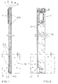
Figur 1 zeigt eine Seitenansicht einer kapazitiven Sensoranordnung. Zunächst wird
in Figur 1 besonders deutlich, daß die Trägerplatten 1, 3 und 5, bis zum Boden des
Behälters ragen, während die als Abstandhalter dazwischenliegenden Zwischenplatten
2 und 4 untere Aussparungen 2.2 und 4.2 aufweisen, durch die das Medium
6 in die sich im Inneren der Zwischenplatten 2 und 4 befindlichen Hohlräume (2.1,
4.1) eindringen kann. Diese Hohlräume werden in späteren Figuren, insbesondere
Fig. 3 und 4 noch näher dargestellt und entsprechend erläutert. Weitere, in Fig. 1
seitlich angeordnete Aussparungen 2.3 und 4.3 im verbleibenden Randbereich der
Zwischenplatten 2 und 4 ermöglichen das Ein- und Ausströmen des Mediums 6 bzw.
den Druckausgleich, so daß sich die Füllhöhe des Mediums 6 innerhalb der Hohlräume
(2.1,4.1) an die Füllhöhe außerhalb der Sensoranordnung anpassen kann.
Der Abstand zwischen den Trägerplatten 1,3 und 5 wird dabei durch die Dicke der
Zwischenplatten 2 und 4 bestimmt und ist vorzugsweise so gewählt, daß die in den
Hohlräumen wirkenden Kapillarkräfte für die Genauigkeit der Füllstandsmessung
vernachlässigbar sind. Figure 1 shows a side view of a capacitive sensor arrangement. First of all
in Figure 1 particularly clearly that the
In dieser bevorzugten Ausgestaltung ist die Außenseite 1.0 der ersten Trägerplatte 1
mit einer Auswerteschaltung 7 ausgestaltet, die noch deutlicher in Figur 2
skizzenhaft in der Vorderansicht dargestellt ist. Außerdem ist ein weiterer Sensor 9
vorgesehen, der beispielsweise die Temperatur oder die chemische Zusammensetzung
oder Qualität des Mediums 6 erfaßt. Das Medium 6 kann prinzipiell flüssig
oder gasförmig sein. Als Ausführungsbeispiel wird ein Ölstandssensor gezeigt, wie er
für Kraftfahrzeuge vorgesehen ist.In this preferred embodiment, the outside is 1.0 of the
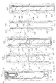
Figur 3 zeigt nun die Vorderseiten 1.0,2.0,3.0,4.0,5.0 der 5 einzelnen Ebenen, also
der Trägerplatten 1, 3 und 5 sowie der Zwischenplatten 2 und 4 in einer Explosionsdarstellung
jeweils seitlich versetzt zueinander. Die Trägerplatten 1, 3 und 5 sind
untereinander durch die Zwischenplatten 2 und 4 hinweg durch metallisierte
Bohrungen, sogenannte Durchkontaktierungen 8 miteinander verbunden, wobei
jeweils entsprechend der zu realisierenden Schaltung jeweils ein Teil der
Durchkontaktierungen 8 über Leitbahnen 1.7,3.4,5.4 mit den Kondensatorbelägen
3.1,5.1, zur Abschirmung dienenden Metallbelägen 1.3,2.7,3.2 oder Bauelementen
7,9 verbunden sind, wie dies anhand der Figur 6 noch näher erläutert werden soll.Figure 3 now shows the front sides 1.0.2.0.3.0.4.0.5.0 of the 5 individual levels, ie
the
In Figur 3 entspricht die Vorderseite der ersten Trägerplatte 1 und damit eine der
zwei Außenseiten der Sensoranordnung der Darstellung aus Figur 2 und zeigt die
Auswerteschaltung 7 mit Leitbahnen 1.7 und Bauelementen sowie einen
Metallbelag 1.3 zur Abschirmung gegen elektromagnetische Felder. Außerdem sind
SMD - Kontaktpunkte für den Sensor 9 zu erkennen.In Figure 3, the front corresponds to the
Versetzt dazu ist die im montierten Zustand darunterliegende Zwischenplatte2
dargestellt, der im unteren Bereich durch einen Randbereich 2.4 umrandet eine
mittlere Aussparung 2.1 aufweist, die einen Hohlraum bildet, in den durch die untere
Aussparung 2.2 und die seitlichen Aussparungen 2.3 das Medium 6 ein- und ausströmen,
insbesondere den Füllstand entsprechend dem Füllstand außerhalb des
Hohlraums anpassen kann. Die einzelnen Abschnitte des Randbereichs 2.4 der
Zwischenplatte 2 dienen als zusätzliche Stabilisierung zwischen den Aussparungen
2.3 und sind vorzugsweise größer als die Aussparungen 2.3. Die Randbereiche 2.4
sind vor dem Freischneiden durch Streben 2.5 untereinander verbunden, wie dies in
Fig. 5 noch deutlicher wird. Die Größe der mittleren Aussparung 2.1 ist angepaßt an
die dazu benachbarten Kondensatorbeläge 1.1 der ersten und 3.1 der zweiten,
mittleren Trägerplatte 3. Der Zwischenplatte2 kann im oberen Bereich zusätzlich mit
einem Metallbelag 2.7 als Abschirmung versehen werden. Der seitlich verbleibende
Randbereich 2.6 ist jeweils im allgemeinen nicht metallisiert, da dort der Kleber zum
Verbinden der Trägerplatten 1,3,5 mit den Zwischenplatten 2,4 aufgebracht wird. The
Die zweite und mittlere Trägerplatte 3 stellt die dritte Ebene der Sensoranordnung
dar und ist zur Ansicht der Vorderseite wiederum versetzt dargestellt. Die zweite
Trägerplatte 3 weist im unteren Bereich einen Kondensatorbelag 3.1 auf, der von
einem metallischen Rand 3.3 umgeben wird, der jedoch vom Kondensatorbelag 3.1
beabstandet bzw. isoliert ist. Der metallische Rand 3.3 dient zur Abschirmung. Er
wird bspw. für Leitbahnen 3.4 zu den einzelnen Kondensatorbelägen unterbrochen.
Zur Abschirmung kann ebenfalls der obere Bereich der Vorderseite zweiten
Trägerplatte 3 mit einem Metallbelag 3.2 versehen und dieser auf Masse geschaltet
werden. Außerdem ist die Leitbahn 3.4 zwischen einer metallischen Bohrung 8 zum
Kondensatorbelag 3.1 zu erkennen.The second and
Die zweite Zwischenplatte 4 in Figur 3 weist nun in diesem Ausführungsbeispiel eine
über die gesamte Länge der Sensoranordnung reichende mittlere Aussparung 4.1
entsprechend dem Kondensatorbelag 5.1 auf der dritten Trägerplatte 5 auf. Seitlich
sind die Randbereiche 4.2 der Zwischenplatte 4 zum Konstanthalten des Abstandes
zwischen den beiden Trägerplatten 3 und 5 bzw. den darauf angeordneten
Kondensatorbelägen 3.6 (3.6 ist auf der Rückseite der zweiten Trägerplatte 3,
dargestellt in Figur 4) und 5.1 angeordnet. Die Zwischenplatte 4 weist untere
Aussparungen 4.2 und seitliche Aussparungen 4.3 für das Medium 6 auf, wobei bei
einer teilweisen Füllung des entstehenden Hohlraums mit dem Medium die oberen
seitlichen Aussparungen 4.3 den Volumen - bzw. Druckausgleich ermöglichen.The second
Wiederum seitlich versetzt ist nun auch die Vorderseite der dritten Platte 5 dargestellt,
die über die gesamte Länge mittig den Kondensatorbelag 5.1 aufweist, der
über eine Leitbahn 5.4 mit einer der metallisierten Bohrungen 8 verbunden und von
einem metallischen Rand 5.3 gegen andere Feldeinflüsse abgeschirmt wird.The front of the
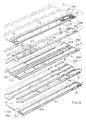
Die Figur 4 zeigt die Rückseiten 1.r,2.r,3.r,4.r,5.r der 5 Ebenen, wobei der
Kondensatorbelag 1.1 auf der Rückseite 1.r der ersten Trägerplatte 1 symmetrisch
zum Kondensatorbelag 3.1 auf der zweiten Trägerplatte 3 ist und mit dieser eine
erste Kondensatoranordnung bildet, die beispielsweise bei Einhaltung einer Mindestfüllhöhe
immer vollständig vom Medium 6 gefüllt ist und daher zur Bestimmung der
relativen Dielektrizitätskonstante des Mediums 6 dient. Die Zwischenplatten 2 und 4
sind vorzugsweise vorder- wie rückseitig identisch. Wiederum sind um die
Kondensatoranordnung 1.1 umlaufende Bahnen 1.4 und zusätzlich auf den freien
Flächen Metallbeläge 1.2 zur Abschirmung vorgesehen.FIG. 4 shows the rear sides 1.r, 2.r, 3.r, 4.r, 5.r of the 5 levels, the
Capacitor coating 1.1 on the back 1.r of the
Die Rückseite 3.r der zweiten Platte 3 weist analog zur Kondensatorbelag 5.1 auf
der Vorderseite der dritten Platte 5 einen Kondensatorbelag 3.6 auf. Diese bilden
die zweite Kondensatoranordnung, die beispielsweise zur Füllhöhenmessung eingesetzt
wird, wobei die aus der ersten Kondensatoranordnung bestimmte Dielektrizitätskonstante
zugrundegelegt wird.The rear side 3.r of the
Außerdem sind in Figur 4 Einlegestreifen 13 angedeutet, der vor dem Verkleben der
Zwischenplatten 2 und 4 mit den benachbarten Trägerplatten 1,3,5 in die mittleren
Aussparungen 2.1,4.1 eingelegt werden und verhindert, daß beim Verkleben durch
die Anpressung die Trägerplatten 1,3,5 verbogen werden. Nachfolgend wird der
Einlegestreifen 13 durch die unteren Aussparungen 2.2.,4.2 wieder entfernt. Die
Rückseite 5.r weist als nach aussen gerichtete Fläche wiederum einen
Abschirmungsbelag 5.2 auf.In addition, insert strips 13 are indicated in
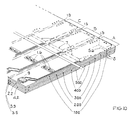
Figur 5 und 10 verdeutlichen die parallele Herstellung mehrerer dieser Sensoranordnungen
gleichzeitig nebeneinander in Mehrebenenleiterplattentechnik, indem auf
den Tafeln 100,300 und 500 aus Trägerplattenmaterial jeweils beabstandet voneinander
mehrere identische Anordnungen erzeugt werden. So weist die Tafel 100
mehrere erste Platten 1 nebeneinander auf und die Tafel 200 mehrere der
Zwischenplatten 2, wobei die einzelnen Segmente über Streben 2.5 miteinander
verbunden sind. Dies setzt sich auf den Tafeln 300 bis 500 entsprechend fort. Alle
diese Tafeln 100 bis 500 werden übereinander ausgerichtet miteinander verklebt
und dann die einzelnen Sensoranordnungen freigeschnitten, wobei die Streben
1.5,2.5,3.5,4.55.5 zwischen den einzelnen Segmenten der Zwischen- und Trägerplatten
1,2,3,4,5 abgetrennt werden.FIGS. 5 and 10 illustrate the parallel production of several of these sensor arrangements
at the same time side by side in multi-level circuit board technology by on
the
Figur 10 verdeutlicht diese gemeinsame Herstellung nochmals, wobei dabei die
Unterteilung der Tafeln 100,200,300,400,500 der Träger- und Zwischenplatten in
Segmente A,B,C,... und deren Verbindung durch die Streben 1.5,2.5,3.5,4.5,5.5
skizzenhaft angedeutet ist. Ausserdem sind die Durchkontaktierungen 8 visualisiert.
Zudem sind die identisch nebeneinander liegenden unteren Einströmöffnungen 4.2
und 2.2 der Hohlräume 2.1 und 4.1 zu erkennen. Während der Hohlraum 4.1 durch
seitliche Öffnungen 4.3 ausgeglichen wird, ist für den Hohlraum 2.1 die andere
Alternative mit einer Öffnung 1.6 in der Trägerplatte 1 gezeigt, die in den Figuren 8
und 9 noch näher gezeigt wird.Figure 10 illustrates this joint production again, with the
Subdivision of the plates 100,200,300,400,500 of the carrier and intermediate plates into
Segments A, B, C, ... and their connection by the struts 1.5.2.5.3.5.4.5.5.5
is sketchily indicated. The plated-through
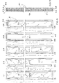
Figur 6 und der daraus vergrößerte Ausschnitt 6a zeigen einen Schnitt durch die
Sensoranordnung bestehend aus den drei Trägerplatten 1, 3 und 5 mit den
Zwischenplatten 2 und 4. Auf den Außenseiten der äußeren Trägerplatten 1 und 5
sind jeweils Metallbeläge 1.3 und 5.2 zur Abschirmung vorgesehen. zur
Abschirmung weisen die Platten im inneren zusätzlich die metallischen Ränder 1.4,
3.3 und 5.3 auf, die gemeinsam ebenfalls auf Masse geschaltet sind. In Figur 6a ist
diejenige metallisierte Bohrung 8 zwischen den fünf Ebenen 1 bis 5 dargestellt, die
diesen Masseanschluß aufweist und mit der dieser Ränder 1.3, 3.3 und 5.3 sowie
die Metallbeläge 1.5 und 5.5 entsprechend über aus Leitbahnen ausgeformte
Kontaktzonen verbunden ist. Die Einbringung der Durchkontaktierungen 8 und
deren Verbindung auf den einzelnen Trägerplatten 1,3,5 ist an sich bereits aus der
Mehrebenen-Leiterplattentechnik bekannt. Dabei werden im Randbereich auf den
jeweiligen Seiten der Trägerplatten 1,3,5 zunächst aus den Leiterbahnen für jeweils
einen Teil der späteren Bohrungen 8 Kontaktzonen ausgebildet. Nach dem Verbinden
der einzelnen Platten 1 bis 5 miteinander werden die Bohrungen 8 eingebracht
und metallisiert. Dabei entsteht ein Kontakt der jeweilige Kontaktzone der
Leiterbahn mit der Metallisierung in der Bohrung 8 und über diese mit einer anderen
Kontaktzone auf einer anderen Trägerplatte. Die Durchkontaktierungen 8 werden
also üblicherweise erst nach dem Verbinden der Träger- und Zwischenplatten 1 bis
5, jedoch vor dem Freischneiden der Segmente aus den Tafeln eingebracht.Figure 6 and the enlarged section 6a show a section through the
Sensor arrangement consisting of the three
Außerdem sind in Figur 6 bzw. 6a die durch die Zwischenplatten 2 und 4 gebildeten
Hohlräume für das Medium und die beidseitig dieser jeweils angeordneten
Kondensatorbeläge 1.1 und 3.1 für die erste Kondensatoranordnung sowie 3.6 und
5.1 für die zweite Kondensatoranordnung zu erkennen. Zusätzlich zeigt Figur 6, wie
die Sensoranordnung in einem Abschirmrohr 11 angeordnet ist, welches auch mit
seinen Öffnungen 12 für das Medium in der Figur 7 dargestellt ist. Die Auswerteschaltung
7 wird durch eine Vergußmasse 10 geschützt. Durch die Verwendung
kupferkaschierter Leiterplatten als Trägerplatten 1,3,5 können durch einen
einfachen Ätzprozeß die Kondensatorbeläge 1.1,3.1,3.6,5.1, Metallbeläge 1.2,1.3,
3.2,5.2 und metallischen Bahnen 1.4,3.3,5.3 der Abschirmungen sowie die Leitbahnen
1.7,3.4,5.4 strukturiert werden. Außerdem sind durch die Mehrebenen-Leiterplattentechnik
bereits geeignete Klebstoffe, Isolationsüberzüge etc. sowie die
Technik zur Metallisierung der Bohrungen 8 bekannt.6 and 6a are those formed by the
Die Figur 8 zeigt in einem weiteren Ausführungsbeispiel die alternative Ausgestaltung
der Öffnungen 1.6 und 5.6 in den Trägerplatten 1 und 5 zum Ein- und
Ausströmen des Mediums 6 in bzw. aus dem jeweiligen Hohlraum 2.1 und 4.1 bzw.
zum Druckausgleich. Veranschaulicht wird diesen Durchströmen bzw. der Druckausgleich
auch anhand eines Schnitts senkrecht durch die Träger- und Zwischenplatten
1-5 in Figur 9, wo durch die Öffnungen 1.6 und 2.2 der Hohlraum 2.1 in der ersten
Zwischenplatte durchströmt wird, während durch die Öffnung 4.2 das Medium 6 in
den Hohlraum 4.1 in der zweiten Zwischenplatte 4 bis zu der im äusseren Behälter
vorliegenden Füllhöhe steigt und durch die Öffnung 5.6 in der unteren Trägerplatte 5
der Druckausgleich erfolgt. 8 shows the alternative embodiment in a further exemplary embodiment
of the openings 1.6 and 5.6 in the
Der Vorteil dieser zweiten Alternative mit den Strömungsöffnungen in den
Trägerplatten 1 und 5 liegt in einem nicht in Abschnitte unterteilten Randbereich 2.4
und 4.4 um den Hohlraum 2.1 bzw. 4.2 herum und eine damit verbundene noch
höhere Stabilität, wobei die Randbereiche der Zwischenplatten 2 und 4 sowie die
Trägerplatten 1,3,5 wiederum durch Streben zunächst miteinander verbunden sind
und nachfolgend entlang dieser freigeschnitten werden. The advantage of this second alternative with the flow openings in the
- 11
- erste Trägerplatte, 1.0 - Vorderseite, 1 .r = Rückseitefirst carrier plate, 1.0 - front, 1 .r = back
- 1.11.1
- Kondensatorbelag (rückseitig)Capacitor coating (rear)
- 1.21.2
- abschirmender Metallbelagshielding metal covering
- 1.31.3
- abschirmender Metallbelagshielding metal covering
- 1.41.4
- umlaufende Abschirmungsbahnall-round shielding path
- 1.51.5
- Strebe zwischen den einzelnen Trägerplattensegmenten der TafelStrut between the individual carrier plate segments of the board
- 1.61.6
-
Löcher als Strömungsöffnungen für das Medium 6Holes as flow openings for the
medium 6 - 1.71.7
- Leitbahnen zwischen Sensor, Auswerteschaltung und DurchkontaktierungenInterconnects between sensor, evaluation circuit and plated-through holes
- 22nd
- Zwischenplatte (2.Ebene), 2.0 = Vorderseite, 2.r = RückseiteIntermediate plate (2nd level), 2.0 = front, 2.r = back
- 2.12.1
- mittlere, den Hohlraum bildende Aussparungmiddle recess forming the cavity
- 2.22.2
- untere Einströmöffnunglower inflow opening
- 2.32.3
-
seitliche Stömungsöffnung in der Zwischenplatte 2lateral flow opening in the
intermediate plate 2 - 2.42.4
- abstandhaltender Randbereich um den Hohlraumspaced edge area around the cavity
- 2.52.5
- Verbindungsträger für die einzelnen AbstandshalterabschnitteConnection carrier for the individual spacer sections
- 2.62.6
- Randzone mit DurchkontaktierungenEdge zone with vias
- 2.72.7
- Abschirmungshielding
- 33rd
- mittlere Trägerplatte (3.Ebene), 3.0 = Vorderseite, 3.r = Rückseitemiddle carrier plate (3rd level), 3.0 = front, 3.r = back
- 3.13.1
- vorderseitiger Kondensatorbelagfront capacitor coating
- 3.23.2
- AbschirmungsbelagShielding covering
- 3.33.3
- AbschirmbahnShielding track
- 3.43.4
- Leitbahn zwischen 8 und 3.1Route between 8 and 3.1
- 3.53.5
- Strebe zwischen den einzelnen Trägerplattensegmenten der TafelStrut between the individual carrier plate segments of the board
- 3.63.6
- rückseitiger Kondensatorbelagback capacitor coating
- 44th
- 2. Zwischenplatte (4.Ebene), 4.0 = Vorderseite, 4.r = Rückseite2nd intermediate plate (4th level), 4.0 = front, 4th r = rear
- 4.14.1
- mittlere, den Hohlraum bildende Aussparungmiddle recess forming the cavity
- 4.24.2
- untere Einströmöffnunglower inflow opening
- 4.34.3
- obere Stömungsöffnungupper flow opening
- 4.44.4
- abstandhatender Randbereichspaced edge area
- 4.54.5
- Trägerstrebe für einzelnen Segmente des AbstandhaltersSupport strut for individual segments of the spacer
- 55
- 3. Trägerplatte (5.Ebene), 5.0 = Vorderseite, 5.r = Rückseite3rd carrier plate (5th level), 5.0 = front, 5th r = back
- 5.15.1
- KondensatorbelagCapacitor coating
- 5.25.2
- abschirmender Metallbelagshielding metal covering
- 5.35.3
- AbschirmbahnShielding track
- 5.45.4
- Leitbahn zwischen Kondensatorbelag und DurchkontaktierungInterconnect between capacitor covering and through-plating
- 5.55.5
- Strebe zwischen den einzelnen Trägerplattensegmenten der TafelStrut between the individual carrier plate segments of the board
- 5.65.6
- Löcher zum Ein- und Ausströmen des Mediums bzw. zum DruckausgleichHoles for the inflow and outflow of the medium or for pressure equalization
- 66
- Mediummedium
- 77
- AuswerteschaltungEvaluation circuit
- 88th
- Vias/DurchkontaktierungenVias / vias
- 99
- Ölqualitätssensor oder TemperatursensorOil quality sensor or temperature sensor
- 1010th
- Vergußmasse zur Fixierung der AuswerteschaltungPotting compound for fixing the evaluation circuit
- 1111
- AbschirmrohrShielding tube
- 1212th
- Strömungsöffnungen im Rohr für das MediumFlow openings in the pipe for the medium
- 1313
- Teflon-EinlagestreifenTeflon insert strips
- 100100
-
Tafel aus Trägerplattenmaterial mit Segmenten A,B,C,... der ersten Trägerplatte 1Plate made of carrier plate material with segments A, B, C, ... of the
first carrier plate 1 - 200200
-
Tafel aus Zwischenplattenmaterial mit Segmenten A,B,C,... der ersten Zwischenplatte 2Plate made of intermediate plate material with segments A, B, C, ... of the first
intermediate plate 2 - 300300
-
Tafel aus Trägerplattenmaterial mit Segmenten A,B,C,... der mittleren Trägerplatte 3Plate made of carrier plate material with segments A, B, C, ... of the
middle carrier plate 3 - 400400
-
Tafel aus Zwischenplattenmaterial mit Segmenten A,B,C,... der ersten Zwischenplatte 2Plate made of intermediate plate material with segments A, B, C, ... of the first
intermediate plate 2 - 500500
-
Tafel aus Trägerplattenmaterial mit Segmenten A,B,C,... der dritten Trägerplatte 5Plate made of carrier plate material with segments A, B, C, ... of the
third carrier plate 5
Claims (14)
Applications Claiming Priority (2)
| Application Number | Priority Date | Filing Date | Title |
|---|---|---|---|
| DE19850245 | 1998-10-31 | ||
| DE19850245A DE19850245A1 (en) | 1998-10-31 | 1998-10-31 | Capacitive sensor arrangement in a liquid or gaseous medium and method for producing it |
Publications (3)
| Publication Number | Publication Date |
|---|---|
| EP0997712A2 true EP0997712A2 (en) | 2000-05-03 |
| EP0997712A3 EP0997712A3 (en) | 2000-07-19 |
| EP0997712B1 EP0997712B1 (en) | 2006-03-22 |
Family
ID=7886269
Family Applications (1)
| Application Number | Title | Priority Date | Filing Date |
|---|---|---|---|
| EP99121294A Expired - Lifetime EP0997712B1 (en) | 1998-10-31 | 1999-10-26 | Capacitive fluid sensing device, manufacturing method and use |
Country Status (3)
| Country | Link |
|---|---|
| US (1) | US6275048B1 (en) |
| EP (1) | EP0997712B1 (en) |
| DE (2) | DE19850245A1 (en) |
Cited By (1)
| Publication number | Priority date | Publication date | Assignee | Title |
|---|---|---|---|---|
| WO2022058752A1 (en) * | 2020-09-21 | 2022-03-24 | Charles Austen Pumps Ltd. | A liquid filter |
Families Citing this family (12)
| Publication number | Priority date | Publication date | Assignee | Title |
|---|---|---|---|---|
| US6781388B2 (en) * | 2001-09-26 | 2004-08-24 | Delphi Technologies, Inc. | Liquid property sensor |
| US6723933B2 (en) | 2001-10-17 | 2004-04-20 | Ronald Helmut Haag | Flexible capacitive strip for use in a non-contact obstacle detection system |
| US6777958B2 (en) | 2001-10-17 | 2004-08-17 | Delphi Technologies, Inc. | Method and apparatus for detecting a change in capacitance of a capacitive proximity sensor |
| US6700393B2 (en) * | 2001-10-17 | 2004-03-02 | Delphi Technologies, Inc. | Capacitive sensor assembly for use in a non-contact obstacle detection system |
| US6750624B2 (en) | 2001-10-17 | 2004-06-15 | Delphi Technologies, Inc. | Non-contact obstacle detection system utilizing ultra sensitive capacitive sensing |
| DE102004004923B4 (en) * | 2004-01-27 | 2012-12-13 | Frank Bayer | Device for capacitive level measurement |
| DE102004053639A1 (en) * | 2004-11-04 | 2006-05-11 | Benjamin Hoffmeier | Device for measuring filling state of liquid in container, e.g. diesel in tank, comprising cascade of measuring probes on plates, e.g. of epoxy resin, with measuring surfaces serving as capacitors |
| DE102005007221A1 (en) * | 2005-02-15 | 2006-09-14 | Hoffmeier, Benjamin | Sensor to monitor the level of liquid stored within a metal or non-metal container has screening capacitor |
| DE102005009093A1 (en) * | 2005-02-22 | 2006-09-07 | Benjamin Hoffmeier | Measuring device for determining filling level in metallic or nonmetallic container, comprises measuring capacitance, reference capacitance and full capacitance for calibration |
| US7475665B2 (en) * | 2006-01-17 | 2009-01-13 | Wacker Neuson Corporation | Capacitance-based fluid level sensor |
| US7863907B2 (en) * | 2007-02-06 | 2011-01-04 | Chevron U.S.A. Inc. | Temperature and pressure transducer |
| CN103995028B (en) * | 2014-06-04 | 2017-01-11 | 江南大学 | Capacitive lampblack concentration sensor |
Citations (6)
| Publication number | Priority date | Publication date | Assignee | Title |
|---|---|---|---|---|
| US3952593A (en) * | 1974-08-01 | 1976-04-27 | Liquidometer Corporation | Liquid level gauge |
| US4589077A (en) * | 1983-07-27 | 1986-05-13 | Southwest Pump Company | Liquid level and volume measuring method and apparatus |
| EP0401111A1 (en) * | 1989-05-31 | 1990-12-05 | Jaeger | Liquid level and/or volume measuring device using a capacitive probe |
| US5142909A (en) * | 1986-09-29 | 1992-09-01 | Baughman James S | Material level indicator |
| US5437184A (en) * | 1993-10-27 | 1995-08-01 | Kdi/Triangle Electronics, Inc. | Capacitive liquid level sensor having phase detecting circuitry |
| FR2752053A1 (en) * | 1996-07-31 | 1998-02-06 | Comm Composants Soc Ind | Reservoir liquid level capacitive measuring sensor used e.g. in fuel tank of vehicle or steam cleaning equipment |
Family Cites Families (4)
| Publication number | Priority date | Publication date | Assignee | Title |
|---|---|---|---|---|
| US4422035A (en) * | 1981-12-11 | 1983-12-20 | Extrude Hone Corporation | Capacitance measurement probe |
| DE4231616C2 (en) * | 1992-09-22 | 1995-08-24 | Seichter Gmbh | Capacitive sensor |
| US5406193A (en) * | 1993-06-23 | 1995-04-11 | Western Research Institute | Hot gas in-situ monitoring probe |
| DE19644777C1 (en) * | 1996-10-28 | 1998-06-04 | Sican Gmbh | Filling level indicator sensors for automobile fuel tank |
-
1998
- 1998-10-31 DE DE19850245A patent/DE19850245A1/en not_active Withdrawn
-
1999
- 1999-10-26 DE DE59913246T patent/DE59913246D1/en not_active Expired - Lifetime
- 1999-10-26 EP EP99121294A patent/EP0997712B1/en not_active Expired - Lifetime
- 1999-11-01 US US09/431,475 patent/US6275048B1/en not_active Expired - Lifetime
Patent Citations (6)
| Publication number | Priority date | Publication date | Assignee | Title |
|---|---|---|---|---|
| US3952593A (en) * | 1974-08-01 | 1976-04-27 | Liquidometer Corporation | Liquid level gauge |
| US4589077A (en) * | 1983-07-27 | 1986-05-13 | Southwest Pump Company | Liquid level and volume measuring method and apparatus |
| US5142909A (en) * | 1986-09-29 | 1992-09-01 | Baughman James S | Material level indicator |
| EP0401111A1 (en) * | 1989-05-31 | 1990-12-05 | Jaeger | Liquid level and/or volume measuring device using a capacitive probe |
| US5437184A (en) * | 1993-10-27 | 1995-08-01 | Kdi/Triangle Electronics, Inc. | Capacitive liquid level sensor having phase detecting circuitry |
| FR2752053A1 (en) * | 1996-07-31 | 1998-02-06 | Comm Composants Soc Ind | Reservoir liquid level capacitive measuring sensor used e.g. in fuel tank of vehicle or steam cleaning equipment |
Cited By (2)
| Publication number | Priority date | Publication date | Assignee | Title |
|---|---|---|---|---|
| WO2022058752A1 (en) * | 2020-09-21 | 2022-03-24 | Charles Austen Pumps Ltd. | A liquid filter |
| GB2599628A (en) * | 2020-09-21 | 2022-04-13 | Charles Austen Pumps Ltd | A liquid filter |
Also Published As
| Publication number | Publication date |
|---|---|
| US6275048B1 (en) | 2001-08-14 |
| EP0997712A3 (en) | 2000-07-19 |
| EP0997712B1 (en) | 2006-03-22 |
| DE19850245A1 (en) | 2000-05-18 |
| DE59913246D1 (en) | 2006-05-11 |
Similar Documents
| Publication | Publication Date | Title |
|---|---|---|
| EP2559327B1 (en) | Method for integrating an electronic component into a printed circuit board | |
| EP1573280B1 (en) | Device and method for measuring capacitance and device for determining the level of a liquid using one such device | |
| DE3605491C2 (en) | ||
| DE2824144C2 (en) | Device for capacitive level measurement of liquids or solids | |
| DE3020196C2 (en) | Multilevel printed circuit board and process for its manufacture | |
| DE19734794A1 (en) | Wiring part and lead frame with the wiring part | |
| EP0997712A2 (en) | Capacitive fluid sensing device and manufacturing method | |
| EP2038624B1 (en) | Electric component comprising a sensor element and method for encapsulating a sensor element | |
| DE2702844A1 (en) | METHOD OF MANUFACTURING A MULTI-LAYER PRINTED CIRCUIT | |
| EP1804557A1 (en) | Electronic safety module | |
| EP1001260A1 (en) | Capacitive sensing arrangement for a gaseous or liquid medium as dielectric | |
| DE19539181C2 (en) | Chip card module and corresponding manufacturing process | |
| EP1804559A2 (en) | Electronic safety module | |
| DE19627543B9 (en) | Multi-layer substrate and method for its production | |
| DE3512237A1 (en) | MULTILAYER FLEXIBLE CIRCUIT ARRANGEMENT WITH CONNECTING DEVICES BETWEEN THE LAYERS | |
| EP1475623B1 (en) | Pressure measuring device with feedthrough connection and procedure for making the connection | |
| DE10311521A1 (en) | Sensor element, especially an oil condition sensor for detecting the state or age of oil, has a plastic body on which metallic sensor elements are directly applied | |
| EP2994722A1 (en) | Scale for a length measuring system, length measuring system and method for producing a length measuring system | |
| EP1238444B1 (en) | Undetachable electrical and mechanical connection, contact element for an undetachable electrical and mechanical connection and method for producing such an electrical and mechanical connection | |
| DE10007967A1 (en) | Multilayer arrangement has conducting track measurement points with openings directing current paths; each point has at least one magnetic difference sensor detecting current in track | |
| EP2679969B1 (en) | Device for detecting the temperature in a room and a method for producing such a device | |
| DE2634702C3 (en) | Electrode arrangement for an electromagnetic flow meter | |
| DE102005014986A1 (en) | Multilayer Technology | |
| EP1804560A2 (en) | Electronic safety module | |
| DE10063251A1 (en) | Wire-contacted pluggable contact arrangement with high density e.g. for electronics and automobiles, uses circuit board having several lamination layers with several sites provided for wire-bonding |
Legal Events
| Date | Code | Title | Description |
|---|---|---|---|
| PUAI | Public reference made under article 153(3) epc to a published international application that has entered the european phase |
Free format text: ORIGINAL CODE: 0009012 |
|
| AK | Designated contracting states |
Kind code of ref document: A2 Designated state(s): DE FR GB IT SE |
|
| AX | Request for extension of the european patent |
Free format text: AL;LT;LV;MK;RO;SI |
|
| PUAL | Search report despatched |
Free format text: ORIGINAL CODE: 0009013 |
|
| AK | Designated contracting states |
Kind code of ref document: A3 Designated state(s): AT BE CH CY DE DK ES FI FR GB GR IE IT LI LU MC NL PT SE |
|
| AX | Request for extension of the european patent |
Free format text: AL;LT;LV;MK;RO;SI |
|
| 17P | Request for examination filed |
Effective date: 20000805 |
|
| AKX | Designation fees paid |
Free format text: DE FR GB IT SE |
|
| RAP1 | Party data changed (applicant data changed or rights of an application transferred) |
Owner name: CONTI TEMIC MICROELECTRONIC GMBH |
|
| 17Q | First examination report despatched |
Effective date: 20050105 |
|
| RTI1 | Title (correction) |
Free format text: CAPACITIVE FLUID SENSING DEVICE, MANUFACTURING METHOD AND USE |
|
| GRAP | Despatch of communication of intention to grant a patent |
Free format text: ORIGINAL CODE: EPIDOSNIGR1 |
|
| GRAS | Grant fee paid |
Free format text: ORIGINAL CODE: EPIDOSNIGR3 |
|
| GRAA | (expected) grant |
Free format text: ORIGINAL CODE: 0009210 |
|
| AK | Designated contracting states |
Kind code of ref document: B1 Designated state(s): DE FR GB IT SE |
|
| PG25 | Lapsed in a contracting state [announced via postgrant information from national office to epo] |
Ref country code: IT Free format text: LAPSE BECAUSE OF FAILURE TO SUBMIT A TRANSLATION OF THE DESCRIPTION OR TO PAY THE FEE WITHIN THE PRESCRIBED TIME-LIMIT;WARNING: LAPSES OF ITALIAN PATENTS WITH EFFECTIVE DATE BEFORE 2007 MAY HAVE OCCURRED AT ANY TIME BEFORE 2007. THE CORRECT EFFECTIVE DATE MAY BE DIFFERENT FROM THE ONE RECORDED. Effective date: 20060322 |
|
| REG | Reference to a national code |
Ref country code: GB Ref legal event code: FG4D Free format text: NOT ENGLISH |
|
| GBT | Gb: translation of ep patent filed (gb section 77(6)(a)/1977) |
Effective date: 20060322 |
|
| REG | Reference to a national code |
Ref country code: SE Ref legal event code: TRGR |
|
| REF | Corresponds to: |
Ref document number: 59913246 Country of ref document: DE Date of ref document: 20060511 Kind code of ref document: P |
|
| ET | Fr: translation filed | ||
| PLBE | No opposition filed within time limit |
Free format text: ORIGINAL CODE: 0009261 |
|
| STAA | Information on the status of an ep patent application or granted ep patent |
Free format text: STATUS: NO OPPOSITION FILED WITHIN TIME LIMIT |
|
| 26N | No opposition filed |
Effective date: 20061227 |
|
| PGFP | Annual fee paid to national office [announced via postgrant information from national office to epo] |
Ref country code: IT Payment date: 20081025 Year of fee payment: 10 Ref country code: SE Payment date: 20081014 Year of fee payment: 10 |
|
| PGFP | Annual fee paid to national office [announced via postgrant information from national office to epo] |
Ref country code: GB Payment date: 20081021 Year of fee payment: 10 |
|
| EUG | Se: european patent has lapsed | ||
| PG25 | Lapsed in a contracting state [announced via postgrant information from national office to epo] |
Ref country code: GB Free format text: LAPSE BECAUSE OF NON-PAYMENT OF DUE FEES Effective date: 20091026 |
|
| PG25 | Lapsed in a contracting state [announced via postgrant information from national office to epo] |
Ref country code: IT Free format text: LAPSE BECAUSE OF NON-PAYMENT OF DUE FEES Effective date: 20091026 |
|
| PG25 | Lapsed in a contracting state [announced via postgrant information from national office to epo] |
Ref country code: SE Free format text: LAPSE BECAUSE OF NON-PAYMENT OF DUE FEES Effective date: 20091027 |
|
| PGFP | Annual fee paid to national office [announced via postgrant information from national office to epo] |
Ref country code: FR Payment date: 20141022 Year of fee payment: 16 Ref country code: DE Payment date: 20141031 Year of fee payment: 16 |
|
| REG | Reference to a national code |
Ref country code: DE Ref legal event code: R119 Ref document number: 59913246 Country of ref document: DE |
|
| PG25 | Lapsed in a contracting state [announced via postgrant information from national office to epo] |
Ref country code: DE Free format text: LAPSE BECAUSE OF NON-PAYMENT OF DUE FEES Effective date: 20160503 |
|
| REG | Reference to a national code |
Ref country code: FR Ref legal event code: ST Effective date: 20160630 |
|
| PG25 | Lapsed in a contracting state [announced via postgrant information from national office to epo] |
Ref country code: FR Free format text: LAPSE BECAUSE OF NON-PAYMENT OF DUE FEES Effective date: 20151102 |