EP0998723B1 - Module and its use in a chip card - Google Patents
Module and its use in a chip card Download PDFInfo
- Publication number
- EP0998723B1 EP0998723B1 EP98947338A EP98947338A EP0998723B1 EP 0998723 B1 EP0998723 B1 EP 0998723B1 EP 98947338 A EP98947338 A EP 98947338A EP 98947338 A EP98947338 A EP 98947338A EP 0998723 B1 EP0998723 B1 EP 0998723B1
- Authority
- EP
- European Patent Office
- Prior art keywords
- module
- chip
- contact elements
- transmission
- transmission module
- Prior art date
- Legal status (The legal status is an assumption and is not a legal conclusion. Google has not performed a legal analysis and makes no representation as to the accuracy of the status listed.)
- Expired - Lifetime
Links
Images

Classifications
-
- G—PHYSICS
- G06—COMPUTING; CALCULATING OR COUNTING
- G06K—GRAPHICAL DATA READING; PRESENTATION OF DATA; RECORD CARRIERS; HANDLING RECORD CARRIERS
- G06K19/00—Record carriers for use with machines and with at least a part designed to carry digital markings
- G06K19/06—Record carriers for use with machines and with at least a part designed to carry digital markings characterised by the kind of the digital marking, e.g. shape, nature, code
- G06K19/067—Record carriers with conductive marks, printed circuits or semiconductor circuit elements, e.g. credit or identity cards also with resonating or responding marks without active components
- G06K19/07—Record carriers with conductive marks, printed circuits or semiconductor circuit elements, e.g. credit or identity cards also with resonating or responding marks without active components with integrated circuit chips
- G06K19/077—Constructional details, e.g. mounting of circuits in the carrier
- G06K19/07745—Mounting details of integrated circuit chips
- G06K19/07747—Mounting details of integrated circuit chips at least one of the integrated circuit chips being mounted as a module
-
- G—PHYSICS
- G06—COMPUTING; CALCULATING OR COUNTING
- G06K—GRAPHICAL DATA READING; PRESENTATION OF DATA; RECORD CARRIERS; HANDLING RECORD CARRIERS
- G06K19/00—Record carriers for use with machines and with at least a part designed to carry digital markings
- G06K19/06—Record carriers for use with machines and with at least a part designed to carry digital markings characterised by the kind of the digital marking, e.g. shape, nature, code
- G06K19/067—Record carriers with conductive marks, printed circuits or semiconductor circuit elements, e.g. credit or identity cards also with resonating or responding marks without active components
- G06K19/07—Record carriers with conductive marks, printed circuits or semiconductor circuit elements, e.g. credit or identity cards also with resonating or responding marks without active components with integrated circuit chips
- G06K19/077—Constructional details, e.g. mounting of circuits in the carrier
- G06K19/07749—Constructional details, e.g. mounting of circuits in the carrier the record carrier being capable of non-contact communication, e.g. constructional details of the antenna of a non-contact smart card
- G06K19/0775—Constructional details, e.g. mounting of circuits in the carrier the record carrier being capable of non-contact communication, e.g. constructional details of the antenna of a non-contact smart card arrangements for connecting the integrated circuit to the antenna
-
- H—ELECTRICITY
- H05—ELECTRIC TECHNIQUES NOT OTHERWISE PROVIDED FOR
- H05K—PRINTED CIRCUITS; CASINGS OR CONSTRUCTIONAL DETAILS OF ELECTRIC APPARATUS; MANUFACTURE OF ASSEMBLAGES OF ELECTRICAL COMPONENTS
- H05K3/00—Apparatus or processes for manufacturing printed circuits
- H05K3/30—Assembling printed circuits with electric components, e.g. with resistor
- H05K3/306—Lead-in-hole components, e.g. affixing or retention before soldering, spacing means
- H05K3/308—Adaptations of leads
-
- H—ELECTRICITY
- H05—ELECTRIC TECHNIQUES NOT OTHERWISE PROVIDED FOR
- H05K—PRINTED CIRCUITS; CASINGS OR CONSTRUCTIONAL DETAILS OF ELECTRIC APPARATUS; MANUFACTURE OF ASSEMBLAGES OF ELECTRICAL COMPONENTS
- H05K2201/00—Indexing scheme relating to printed circuits covered by H05K1/00
- H05K2201/10—Details of components or other objects attached to or integrated in a printed circuit board
- H05K2201/10431—Details of mounted components
- H05K2201/1059—Connections made by press-fit insertion
-
- H—ELECTRICITY
- H05—ELECTRIC TECHNIQUES NOT OTHERWISE PROVIDED FOR
- H05K—PRINTED CIRCUITS; CASINGS OR CONSTRUCTIONAL DETAILS OF ELECTRIC APPARATUS; MANUFACTURE OF ASSEMBLAGES OF ELECTRICAL COMPONENTS
- H05K2201/00—Indexing scheme relating to printed circuits covered by H05K1/00
- H05K2201/10—Details of components or other objects attached to or integrated in a printed circuit board
- H05K2201/10613—Details of electrical connections of non-printed components, e.g. special leads
- H05K2201/10621—Components characterised by their electrical contacts
- H05K2201/10689—Leaded Integrated Circuit [IC] package, e.g. dual-in-line [DIL]
-
- H—ELECTRICITY
- H05—ELECTRIC TECHNIQUES NOT OTHERWISE PROVIDED FOR
- H05K—PRINTED CIRCUITS; CASINGS OR CONSTRUCTIONAL DETAILS OF ELECTRIC APPARATUS; MANUFACTURE OF ASSEMBLAGES OF ELECTRICAL COMPONENTS
- H05K2201/00—Indexing scheme relating to printed circuits covered by H05K1/00
- H05K2201/10—Details of components or other objects attached to or integrated in a printed circuit board
- H05K2201/10613—Details of electrical connections of non-printed components, e.g. special leads
- H05K2201/10742—Details of leads
- H05K2201/1075—Shape details
- H05K2201/1078—Leads having locally deformed portion, e.g. for retention
-
- H—ELECTRICITY
- H05—ELECTRIC TECHNIQUES NOT OTHERWISE PROVIDED FOR
- H05K—PRINTED CIRCUITS; CASINGS OR CONSTRUCTIONAL DETAILS OF ELECTRIC APPARATUS; MANUFACTURE OF ASSEMBLAGES OF ELECTRICAL COMPONENTS
- H05K2203/00—Indexing scheme relating to apparatus or processes for manufacturing printed circuits covered by H05K3/00
- H05K2203/14—Related to the order of processing steps
- H05K2203/1446—Treatment after insertion of lead into hole, e.g. bending, cutting, caulking or curing of adhesive but excluding soldering
Definitions
- DE 195 00 925 A1 describes a chip card for contactless Data transmission known, on the one hand, a chip module with a integrated circuit and secondly a transmission module with at least one transmission element for data and / or Energy transfer between the integrated circuit and an external device.
- the transmission module in the card body integrated.
- the chip module inserted into a recess in the card body created for this purpose and connected to it.
- the transmission module For electrical coupling of the chip module to the transmission module are the corresponding Contact elements of the chip module on the one hand and the Transmission module placed on the other hand.
- a contactless Chip card a chip module and a transmission module to one module to connect and keep ready as a semi-finished product, the corresponding contact elements from the chip module on the one hand and the transmission module on the other hand by soldering or insertion a conductive adhesive electrically connected together are.
- the chip and the transmission module are on a common carrier attached between at least two carrier layers of the card body is embedded, so that after the lamination of the carrier layers, the chip card is produced is.
- connection type of soldering is that due to the high temperature load that from a thermoplastic Plastic existing transmission module is very heavily used becomes, so that deformation thereof occurs can. Furthermore, the soldering process is relatively complex because it is additional Soldering agent applied to the transmission module Need to become.
- a disadvantage of the electrically conductive adhesive is that as a result As it ages, its conductivity decreases. Furthermore is the thickness of the electrically conductive adhesive in terms of process technology difficult to set to a constant value. The Setting a constant distance between the corresponding ones However, contact elements are required for the Transverse extension of the module in this contact area with the Depth of the intended recess of the card body matches.
- WO 98/06063 A1 it is used to connect a chip module known with a transmission module, a contact piece with a provide intersecting geometry, with the contact piece extends in an opening of the transmission module and a establishes an electrically conductive connection to an antenna of the same.
- DE 44 40 721 A1 describes a module consisting of two with one another known to connect flat support layers, at of the two carrier layers on one facing the other
- pointed mandrels and corresponding to it have recordings on the other side.
- the mandrels corresponding to the two carrier layers positioned the shots, after bending them are clamped in the recordings.
- a disadvantage of the known Module is that a precise position of the carrier-carrier layers must be given to each other. Claim 1 is against delimited this document.
- the object of the present invention is to provide a module of this type further education in a simple way a reliable and safe electrical contact between a chip module and to ensure another component.
- the invention has the features of Claim 1 on.
- the particular advantage of the module according to the invention is that that only cutting elements must be provided in order to a jamming contact of a chip module with a transmission module to enable. This can be a simple and reliable electrical contacting can be created.
- the contacting also serves as a mechanical connection of the chip module with the transmission module. They are advantageous Contact elements are not exposed to temperature stress.
- the Connection is made solely by using a contact pressure.
- a module can be easily manufactured as a semi-finished product that always has the same training. This is achieved in particular by the fact that the contact elements even the deadlock is generated. There are no others additional materials or components required to complete the to bring about electrical contacting. Kindness and training The contact is made solely by the materials of the Contact elements determined themselves.
- the Contact elements of the chip module each as a crown-shaped Cutting contacts formed, the tapering points of the Cutting contact through a carrier layer of the transmission module are pushable. By redirecting and pressing them in the direction of the contact element of the transmission module a flat press fit of the prongs on the contact elements of the Transmission module created.
- the contact elements of the chip module part of a metallic chip carrier layer can preferably be a sheet metal part be formed, the shape of the contact element simple be produced by cutting or bending tools can.
- the chip module is on one facing away from the contact elements of the transmission module Side connected to the same so that applying an intermediate Insulation layer is not required.
- a defined majesty of the module is advantageously guaranteed, so the recess of the card body accordingly is customizable.
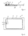
- FIG. 1 shows a module 1, which consists of a transmission module 2 and a chip module 3 is composed. The connection between the transmission module 2 and the chip module 3 takes place in a contacting area of the same.
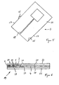
- the transmission module 2 from a transfer carrier layer 4, on which a transfer element 5 as structured, in particular etching technology, Printing or laser-structured, printed coil printed or is applied as a wire-wound coil.
- the Transmission element 5 is designed as an antenna and is used for Data and / or energy transmission between one in FIG. 3 shown chip 6 and an external device. That several turns having transmission element 5 has at its ends flat contact elements 7. Alternatively, the contact elements 7 can also be round or raised.
- the transmission module 2 has a cutout 8 on, which are adjacent to that formed by the contact elements 7 Contacting area.
- the transfer carrier layer 4 is made of a flexible plastic material PVC, PC or ABS with a thickness of at least 150 microns, preferably 200 to 300 ⁇ m.
- a chip module 3 consists of one thin cuboidal chip carrier layer 10, which is preferably is formed from a metallic material.
- the integrated circuit 6 is applied to the chip carrier layer 10, its electrical connections through contact elements 11 be formed.
- the contact elements 11 are crown-shaped Cutting contacts 12 with protruding at right angles and tapering Jagged 13 formed.
- the formation of the contact elements 11 is carried out by appropriate cutting and bending tools. By punching 9, the contact elements 11 are apart separated and isolated.
- the chip module 3 can be used as an intermediate product be kept ready on a roll.
- the press fit is increased by the thickness the point 13 is substantially larger than the thickness of the contact elements 7, preferably twice as large as the transverse extent the contact elements 7. It becomes a permanent clamping connection created between the contact elements 7 and 11, wherein a predetermined by the thickness of the contact elements 7 and 11 Majesty of module 1 is formed.
- the chip carrier layer 10 can only have incisions, in particular cross-shaped incisions. Only at the Establishing the connection between the chip module 3 and the Transmission module 2 is by tipping or swiveling the through the incisions formed prongs 13 from one with the Chip carrier layer 10 common level, the contact element 11 formed, which then corresponds to the contact element 7 in plant brought. In this embodiment, formation occurs the cutting contacts 12 so only immediately when connected of the chip module 3 with the transmission module 2. The chip module 3 can thus essentially without protruding contact elements 11 are kept ready, so that the manufacturing Effort is reduced.
- the contact elements are designed as contact lugs 15.
- the contact lugs 15 each correspond to a corresponding one Contact surface of the transmission module on one edge 17 of a chip carrier layer 16 is arranged.
- the contact lugs 15 are triangular. Alternatively, they can also be designed in the form of an arc. It is important that the area of the contact elements 15 is so large is that after bending the same a sufficiently large contact area is formed, which is flat on the corresponding Contact element of the transmission module rests.
- a slot 18 separates the contact elements 15 from one another, so that there is no electrical connection between them.
- the contact elements of the chip module can also be used the provision of marginal incisions in a cuboid Chip carrier layer are formed, so less material is required.
- the formation of at least one contact element are formed by the course of the insulating slot, so that the manufacturing outlay is further reduced can be.
- the contact elements can therefore on any Place of the chip carrier layer may be arranged, preferably but in an edge area. They are part of the chip carrier layer formed so that the chip carrier layer has a double Function. On the one hand, it serves as a carrier layer for the chip and the other to form contact elements.
- the chip carrier layer is made of an electrically conductive material formed, preferably from sheet metal.
- the modules described above serve as semi-finished products for the production of a chip card 19, as shown in Figure 6 is.
- the chip card 19 can be produced in the laminating technology , each being adjacent to the transfer carrier layer 4 and the chip carrier layer 10 an inner Core layer 20 connects.
- the core layers 20 each have to the elevations of the transfer carrier layer 4 and the chip carrier layer 10 corresponding recesses 21.
- the core layers 20 and the cover layers 22 can consist of an ABS, PC or PVC material.
Abstract
Description
Aus der DE 195 00 925 A1 ist eine Chipkarte zur kontaktlosen Datenübertragung bekannt, die zum einen ein Chipmodul mit einem integrierten Schaltkreis und zum anderen ein Übertragungsmodul mit mindestens einem Übertragungselement zur Daten- und/oder Energieübertragung zwischen dem integrierten Schaltkreis und einem externen Gerät aufweist. Zur Bildung der Chipkarte wird in einem ersten Schritt das Übertragungsmodul in den Kartenkörper integriert. In einem zweiten Schritt wird dann das Chipmodul in eine dafür geschaffene Ausnehmung des Kartenkörpers eingesetzt und mit demselben verbunden. Zur elektrischen Ankopplung des Chipmoduls an das Übertragungsmodul werden die korrespondierenden Kontaktelemente des Chipmoduls einerseits und des Übertragungsmoduls andererseits aneinandergelegt. Dabei kann die elektrische Kontaktierung zwischen den korrespondierenden Kontaktelementen mittels Verlötung, durch Einbringen eines leitfähigen Klebers oder eines elastisch deformierbaren Körpers zwischen den Kontaktelementen hergestellt werden. Diese bekannten Kontaktierungsarten sind relativ aufwendig und unterliegen infolge starker Biegebeanspruchung der Chipkarte nur einer begrenzten Lebensdauer.DE 195 00 925 A1 describes a chip card for contactless Data transmission known, on the one hand, a chip module with a integrated circuit and secondly a transmission module with at least one transmission element for data and / or Energy transfer between the integrated circuit and an external device. For the formation of the chip card in a first step the transmission module in the card body integrated. In a second step, the chip module inserted into a recess in the card body created for this purpose and connected to it. For electrical coupling of the chip module to the transmission module are the corresponding Contact elements of the chip module on the one hand and the Transmission module placed on the other hand. It can the electrical contact between the corresponding ones Contact elements by means of soldering, by introducing a conductive adhesive or an elastically deformable body be made between the contact elements. These well-known Contact types are relatively complex and subject to due to strong bending stress on the chip card only a limited one Lifespan.
Weiterhin ist es bekannt, zur Herstellung einer kontaktlosen Chipkarte ein Chipmodul und ein Übertragungsmodul zu einem Modul zu verbinden und als Halbzeug bereitzuhalten, wobei die korrespondierenden Kontaktelemente von dem Chipmodul einerseits und dem Übertragungsmodul andererseits durch Löten bzw. Einbringen eines leitfähigen Klebers elektrisch miteinander verbunden sind. Dabei sind das Chip- und das Übertragungsmodul auf einem gemeinsamen Träger angebracht, der zwischen mindestens zwei Trägerschichten des Kartenkörpers eingebettet wird, so dass nach Laminieren der Trägerschichten die Chipkarte hergestellt ist.Furthermore, it is known to produce a contactless Chip card a chip module and a transmission module to one module to connect and keep ready as a semi-finished product, the corresponding contact elements from the chip module on the one hand and the transmission module on the other hand by soldering or insertion a conductive adhesive electrically connected together are. The chip and the transmission module are on a common carrier attached between at least two carrier layers of the card body is embedded, so that after the lamination of the carrier layers, the chip card is produced is.
Nachteilig an der bekannten Verbindungsart des Lötens ist, dass infolge der hohen Temperaturbelastung das aus einem thermoplastischen Kunststoff bestehende Übertragungsmodul sehr stark beansprucht wird, so dass eine Verformung desselben eintreten kann. Weiterhin ist der Lötvorgang relativ aufwendig, da zusätzlich Lötstoppmittel auf das Übertragungsmodul aufgebracht werden müssen.A disadvantage of the known connection type of soldering is that due to the high temperature load that from a thermoplastic Plastic existing transmission module is very heavily used becomes, so that deformation thereof occurs can. Furthermore, the soldering process is relatively complex because it is additional Soldering agent applied to the transmission module Need to become.
Nachteilig an dem elektrisch leitenden Kleber ist, dass infolge Alterung desselben seine Leiteigenschaften abnehmen. Ferner ist die Dicke des elektrisch leitenden Klebers prozesstechnisch schwer auf einen konstanten Wert eingestellt werden kann. Die Einstellung eines konstanten Abstandes zwischen den korrespondierenden Kontaktelementen ist jedoch erforderlich, damit die Quererstreckung des Moduls in diesem Kontaktbereich mit der Tiefe der dafür vorgesehenen Ausnehmung des Kartenkörpers übereinstimmt.A disadvantage of the electrically conductive adhesive is that as a result As it ages, its conductivity decreases. Furthermore is the thickness of the electrically conductive adhesive in terms of process technology difficult to set to a constant value. The Setting a constant distance between the corresponding ones However, contact elements are required for the Transverse extension of the module in this contact area with the Depth of the intended recess of the card body matches.
Aus der WO 98/06063 A1 ist es zur Verbindung eines Chipmoduls mit einem Übertragungsmodul bekannt, ein Kontaktstück mit einer schneidenden Geometrie vorzusehen, wobei sich das Kontaktstück in einer Öffnung des Übertragungsmoduls erstreckt und eine elektrisch leitende Verbindung zu einer Antenne desselben herstellt.From WO 98/06063 A1 it is used to connect a chip module known with a transmission module, a contact piece with a provide intersecting geometry, with the contact piece extends in an opening of the transmission module and a establishes an electrically conductive connection to an antenna of the same.
Aus der US 5 598 032 A ist es zur Verbindung von einem Chipmodul mit einem Übertragungsmodul bekannt, metallische Zungen vorzusehen. Ein Einschneiden dieser Zungen durch die Trägerschicht des Chipmoduls ist nicht vorgesehen.From US 5 598 032 A it is for the connection of a chip module known with a transmission module, metallic tongues provided. Incision of these tongues through the backing the chip module is not provided.
Aus der DE 44 40 721 A1 ist ein Modul bestehend aus zwei miteinander
zu verbindenden flächigen Trägerschichten bekannt, bei
der die beiden Trägerschichten auf einer zueinandergekehrten
Seite zum einen spitz zulaufende Dorne und korrespondierend dazu
auf der anderen Seite Aufnahmen aufweisen. Zur Verbindung
der beiden Trägerschichten werden die Dorne korrespondierend zu
den Aufnahmen positioniert, wobei sie nach Verbiegen derselben
klemmend in den Aufnahmen gehaltert sind. Nachteilig an dem bekannten
Modul ist, dass eine positionsgenaue Anlage der Träger-Trägerschichten
zueinander gegeben sein muss. Anspruch 1 ist gegen
dieses Dokument abgegrenzt.DE 44 40 721 A1 describes a module consisting of two with one another
known to connect flat support layers, at
of the two carrier layers on one facing the other
On the one hand, pointed mandrels and corresponding to it
have recordings on the other side. For connection
the mandrels corresponding to the two carrier layers
positioned the shots, after bending them
are clamped in the recordings. A disadvantage of the known
Module is that a precise position of the carrier-carrier layers
must be given to each other.
Aufgabe der vorliegenden Erfindung ist es, ein Modul derart weiterzubilden, um auf einfache Weise eine zuverlässige und sichere elektrische Kontaktierung zwischen einem Chipmodul und einem weiteren Bauteil zu gewährleisten.The object of the present invention is to provide a module of this type further education in a simple way a reliable and safe electrical contact between a chip module and to ensure another component.
Zur Lösung dieser Aufgabe weist die Erfindung die Merkmale des
Patentanspruchs 1 auf.To achieve this object, the invention has the features of
Der besondere Vorteil des erfindungsgemäßen Moduls besteht darin, dass lediglich Schneidelemente vorgesehen sein müssen, um eine klemmende Kontaktierung eines Chipmoduls mit einem Übertragungsmodul zu ermöglichen. Hierdurch kann eine einfache und zuverlässige elektrische Kontaktierung geschaffen werden.The particular advantage of the module according to the invention is that that only cutting elements must be provided in order to a jamming contact of a chip module with a transmission module to enable. This can be a simple and reliable electrical contacting can be created.
Zusätzlich dient die Kontaktierung zur mechanischen Verbindung des Chipmoduls mit dem Übertragungsmodul. Vorteilhaft sind die Kontaktelemente keiner Temperaturbeanspruchung ausgesetzt. Die Verbindung erfolgt allein durch Ausnutzung einer Anpresskraft. The contacting also serves as a mechanical connection of the chip module with the transmission module. They are advantageous Contact elements are not exposed to temperature stress. The Connection is made solely by using a contact pressure.
Auf einfache Weise kann ein Modul als Halbzeug hergestellt werden, das stets eine gleichbleibende Ausbildung aufweist. Dies wird insbesondere dadurch erzielt, dass durch die Kontaktelemente selbst die Verklemmung erzeugt wird. Es sind keine weiteren zusätzlichen Materialien oder Bauteile erforderlich, um die elektrische Kontaktierung herbeizuführen. Die Güte und die Ausbildung der Kontaktierung wird allein durch die Materialien der Kontaktelemente selbst bestimmt.A module can be easily manufactured as a semi-finished product that always has the same training. This is achieved in particular by the fact that the contact elements even the deadlock is generated. There are no others additional materials or components required to complete the to bring about electrical contacting. Kindness and training The contact is made solely by the materials of the Contact elements determined themselves.
Nach einer besonderen Ausführungsform der Erfindung sind die Kontaktelemente des Chipmoduls jeweils als kronenförmige Schneidkontakte ausgebildet, wobei spitz zulaufende Zacken des Schneidkontaktes durch eine Trägerschicht des Übertragungsmoduls durchdrückbar sind. Durch Umlenkung und Andrücken derselben in Richtung des Kontaktelements des Übertragungsmoduls wird ein flächiger Presssitz der Zacken auf den Kontaktelementen des Übertragungsmoduls geschaffen.According to a particular embodiment of the invention, the Contact elements of the chip module each as a crown-shaped Cutting contacts formed, the tapering points of the Cutting contact through a carrier layer of the transmission module are pushable. By redirecting and pressing them in the direction of the contact element of the transmission module a flat press fit of the prongs on the contact elements of the Transmission module created.
Nach einer Weiterbildung der Erfindung sind die Kontaktelemente des Chipmoduls Bestandteil einer metallischen Chipträgerschicht. Vorzugsweise kann die Chipträgerschicht als Blechteil ausgebildet sein, wobei die Formgebung des Kontaktelements einfach durch Schneid- bzw. Biegewerkzeuge hergestellt werden kann.According to a development of the invention, the contact elements of the chip module part of a metallic chip carrier layer. The chip carrier layer can preferably be a sheet metal part be formed, the shape of the contact element simple be produced by cutting or bending tools can.
Nach einer Weiterbildung der Erfindung wird das Chipmodul an einer den Kontaktelementen des Übertragungsmoduls abgewandten Seite mit demselben verbunden, so dass das Auftragen einer zwischenliegenden Isolationsschicht nicht erforderlich ist.According to a development of the invention, the chip module is on one facing away from the contact elements of the transmission module Side connected to the same so that applying an intermediate Insulation layer is not required.
Vorteilhaft wird eine definierte Erhabenheit des Moduls gewährleistet, so dass die Aussparung des Kartenkörpers entsprechend anpassbar ist. Dadurch, dass die Chipträgerschicht von der Rückseite her an die Übertragungsträgerschicht andrückbar ist, wobei der Chip in eine korrespondierende Ausnehmung der Übertragungsmodulschicht eingreift, wird ein Modul mit vergleichsweise geringer Quererstreckung im Chipbereich geschaffen.A defined majesty of the module is advantageously guaranteed, so the recess of the card body accordingly is customizable. The fact that the chip carrier layer from the Back can be pressed against the transfer carrier layer, wherein the chip in a corresponding recess of the transmission module layer intervenes, a module with comparative low transverse extension in the chip area.
Ausführungsbeispiele der Erfindung werden nachfolgend anhand der Zeichnungen näher erläutert.Exemplary embodiments of the invention are described below of the drawings explained in more detail.
Es zeigen:
Figur 1- Einen Teillängsschnitt durch ein Modul,
Figur 2- eine Draufsicht auf ein Übertragungsmodul,
Figur 3- eine perspektivische Ansicht eines Chipmoduls nach einem ersten Ausführungsbeispiel,
Figur 4- einen Querschnitt durch ein Kontaktelement gemäß
Figur 3, Figur 5- eine perspektivische Ansicht auf ein Chipmodul mit Kontaktelementen nach einem zweiten Ausführungsbeispiel und
Figur 6- einen Längsschnitt durch eine Chipkarte mit einem erfindungsgemäßen Modul.
- Figure 1
- A partial longitudinal section through a module,
- Figure 2
- a plan view of a transmission module,
- Figure 3
- 2 shows a perspective view of a chip module according to a first exemplary embodiment,
- Figure 4
- 3 shows a cross section through a contact element according to FIG. 3,
- Figure 5
- a perspective view of a chip module with contact elements according to a second embodiment and
- Figure 6
- a longitudinal section through a chip card with a module according to the invention.
Figur 1 zeigt ein Modul 1, das aus einem Übertragungsmodul 2
und einem Chipmodul 3 zusammengesetzt ist. Die Verbindung zwischen
dem Übertragungsmodul 2 und dem Chipmodul 3 erfolgt in
einem Kontaktierungsbereich derselben.FIG. 1 shows a
Wie aus Figur 2 zu ersehen ist, besteht das Übertragungsmodul 2
aus einer Übertragungsträgerschicht 4, auf der ein Übertragungselement
5 als strukturierte, insbesondere ätztechnisch,
drucktechnisch oder laserstrukturiert aufgebrachte, Spule aufgedruckt
oder als drahtgewickelte Spule aufgebracht ist. Das
Übertragungselement 5 ist als Antenne ausgebildet und dient zur
Daten- und/oder Energieübertragung zwischen einem in Figur 3
dargestellten Chip 6 und einem externen Gerät. Das mehrere Windungen
aufweisende Übertragungselement 5 weist an seinen Enden
flächige Kontaktelemente 7 auf. Alternativ können die Kontaktelemente
7 auch rund oder erhaben ausgebildet sein. Zur Aufnahme
des Chips 6 weist das Übertragungsmodul 2 eine Aussparung 8
auf, die sich benachbart zu dem durch die Kontaktelemente 7 gebildeten
Kontaktierungsbereich befindet. Die Übertragungsträgerschicht
4 besteht aus einem flexiblen Kunststoffmaterial aus
PVC, PC oder ABS mit einer Dicke von mindestens 150 µm, vorzugsweise
200 bis 300 µm.As can be seen from FIG. 2, there is the
Wie aus Figur 3 zu ersehen ist, besteht ein Chipmodul 3 aus einer
dünnen quaderförmigen Chipträgerschicht 10, die vorzugsweise
aus einem metallischen Werkstoff gebildet wird. Auf der
Chipträgerschicht 10 ist der integrierte Schaltkreis 6 aufgebracht,
dessen elektrische Anschlüsse durch Kontaktelemente 11
gebildet werden. Die Kontaktelemente 11 sind als kronenförmige
Schneidkontakte 12 mit rechtwinklig abstehenden und spitz zulaufenden
Zacken 13 ausgebildet. Die Ausbildung der Kontaktelemente
11 erfolgt durch entsprechende Schneid- und Biegewerkzeuge.
Durch Ausstanzungen 9 sind die Kontaktelemente 11 voneinander
getrennt und isoliert. Das Chipmodul 3 kann als Zwischenerzeugnis
auf einer Rolle bereitgehalten werden.As can be seen from FIG. 3, a
Zur Herstellung einer elektrischen und mechanischen Verbindung
zwischen dem Chipmodul 3 und dem Übertragungsmodul 2 werden die
Übertragungsträgerschicht 4 und die Chipträgerschicht 10 derart
aneinandergelegt, dass der integrierte Schaltkreis 6 mit der
Aussparung 8 fluchtet und die Zacken 13 der Schneidkontakte 12
korrespondierend zu den Kontaktelementen 7 an der Rückseite der
Übertragungsträgerschicht 4 anliegen. Durch Ausübung einer
Kraft in Richtung der Kontakelemente 7 werden die Zacken 13 der
Kontaktelemente 11 durch die Übertragungsträgerschicht 4 bzw.
durch das korrespondierenden Kontaktelemente 7 hindurchgedrückt,
so dass die Übertragungsträgerschicht 4 und die Chipträgerschicht
10 flächig aneinanderliegen. Durch geeignete Biegewerkzeuge
werden die Zacken 13 umgebogen und auf die Fläche
des entsprechenden Kontaktelements 7 gedrückt. Die Zacken 13
liegen plan unter Bildung eines Preßsitzes auf den Kontaktelementen
7 an. Der Preßsitz wird dadurch erhöht, dass die Dicke
der Zacken 13 wesentlich größer ist als die Dicke der Kontaktelemente
7, vorzugsweise doppelt so groß wie die Quererstreckung
der Kontaktelemente 7. Es wird eine dauerhafte klemmende Verbindung
zwischen den Kontaktelementen 7 und 11 geschaffen, wobei
eine durch die Dicke der Kontaktelemente 7 und 11 vorgegebene
Erhabenheit des Moduls 1 gebildet wird.For establishing an electrical and mechanical connection
between the
Alternativ kann die Chipträgerschicht 10 lediglich Einschnitte,
insbesondere kreuzförmige Einschnitte, aufweisen. Erst bei der
Herstellung der Verbindung zwischen dem Chipmodul 3 und dem
Übertragungsmodul 2 wird durch Auftulpen bzw. Verschwenken der
durch die Einschnitte gebildeten Zacken 13 aus einer mit der
Chipträgerschicht 10 gemeinsamen Ebene das Kontaktelement 11
gebildet, das dann korrespondierend zum Kontaktelement 7 in Anlage
gebracht wird. Bei dieser Ausführungsform erfolgt die Bildung
der Schneidkontakte 12 also erst unmittelbar bei Verbindung
des Chipmoduls 3 mit dem Übertragungsmodul 2. Das Chipmodul
3 kann somit im wesentlichen ohne abstehende Kontaktelemente
11 bereitgehalten werden, so dass der herstellungstechnische
Aufwand reduziert ist.Alternatively, the
Nach einer weiteren Ausführungsform des Chipmoduls 3 gemäß Figur
5 sind die Kontaktelemente als Kontaktnasen 15 ausgebildet.
Die Kontaktnasen 15 sind jeweils korrespondierend zu einer entsprechenden
Kontaktfläche des Übertragungsmoduls an einem Rand
17 einer Chipträgerschicht 16 angeordnet. Wie aus Figur 5 ersichtlich
ist, sind die Kontaktnasen 15 dreieckförmig ausgebildet.
Alternativ können sie auch bogenförmig ausgebildet sein.
Wichtig ist, dass die Fläche der Kontaktelemente 15 so groß
ist, dass nach Umbiegung derselben eine ausreichend große Kontaktfläche
gebildet wird, die flächig auf dem korrespondierenden
Kontaktelement des Übertragungsmoduls aufliegt.According to a further embodiment of the
Ein Schlitz 18 trennt die Kontaktelemente 15 voneinander, so
dass keine elektrische Verbindung zwischen ihnen besteht. Durch
Verschwenken der Kontaktnasen 15 um einen nicht dargestellten
Rand des Übertragungsmoduls kann eine klemmende elektrische und
zugleich mechanische Verbindung zwischen der Chipträgerschicht
16 und dem Übertragungsmodul geschaffen werden.A
Alternativ können die Kontaktelemente des Chipmoduls auch durch das Vorsehen von randseitigen Einschnitten in eine quaderförmige Chipträgerschicht gebildet werden, so dass weniger Materialaufwand erforderlich ist.Alternatively, the contact elements of the chip module can also be used the provision of marginal incisions in a cuboid Chip carrier layer are formed, so less material is required.
Alternativ kann die Ausbildung zumindest eines Kontaktelements durch den Verlauf des isolierenden Schlitzes gebildet werden, so dass der herstellungstechnische Aufwand weiter verringert werden kann. Die Kontaktelemente können also an einer beliebigen Stelle der Chipträgerschicht angeordnet sein, vorzugsweise aber in einem Randbereich. Sie sind als Teil der Chipträgerschicht ausgebildet, so dass der Chipträgerschicht eine doppelte Funktion zukommt. Sie dient zum einen als Trägerschicht für den Chip und zum anderen zur Ausbildung von Kontaktelementen. Die Chipträgerschicht ist aus einem elektrisch leitenden Material gebildet, vorzugsweise aus Blech. Alternatively, the formation of at least one contact element are formed by the course of the insulating slot, so that the manufacturing outlay is further reduced can be. The contact elements can therefore on any Place of the chip carrier layer may be arranged, preferably but in an edge area. They are part of the chip carrier layer formed so that the chip carrier layer has a double Function. On the one hand, it serves as a carrier layer for the chip and the other to form contact elements. The chip carrier layer is made of an electrically conductive material formed, preferably from sheet metal.
Die oben beschriebenen Module dienen jeweils als Halbzeug für
die Herstellung einer Chipkarte 19, wie sie in Figur 6 dargestellt
ist. Die Chipkarte 19 kann in der Laminiertechnik hergestellt
werden, wobei sich jeweils benachbart zu der Übertragungsträgerschicht
4 und der Chipträgerschicht 10 eine innere
Kernschicht 20 anschließt. Die Kernschichten 20 weisen jeweils
zu den Erhebungen der Übertragungsträgerschicht 4 und der Chipträgerschicht
10 korrespondierende Ausnehmungen 21 auf. Außenseitig
schließen sich an die Kernschichten 20 jeweils eine
Deckschicht 22 an, deren Außenflächen vorzugsweise mit einem
Aufdruck versehen sind. Die Kernschichten 20 und die Deckschichten
22 können aus einem ABS-, PC- oder PVC-Material bestehen.The modules described above serve as semi-finished products for
the production of a
Claims (6)
- Module, particularly for use in chip cards, comprising a chip module (3) with an integrated circuit (6) on one hand and a transmission module (2) with a transmission element (5) for transmitting data and/or energy between the integrated circuit (6) and an external unit or vice versa on the other hand, wherein said chip module (3) and said transmission module (2) each comprise carrier substrates (4, 10) and contact elements (7, 11) for electric interconnection; wherein said chip module (3) or said transmission module (2) is provided with flexible interconnection elements (12) to establish positive mechanical and electric connection therebetween; and wherein the interconnection element (12) is clampingly engageable with one side of the carrier substrate (4, 10);
characterized by the fact that
the interconnection element (12) is provided in the form of a cutting element such that on having been pressed through the carrier substrate (4, 10) of the chip module (3) or the transmission module (2), respectively, said interconnection element will act to establish full-face engagement between said chip module (3) and said transmission module (2). - Module according to Claim 1, characterized by the fact that the cutting element (12) is provided as contact element (11) of said chip module (3) and comprises protruding prongs (13) which while in bent contacting position are engaging the corresponding contact element (7) of said transmission module (2).
- Module according to Claims 1 or 2, characterized by the fact that said chip module (3) comprises a chip carrier substrate (10) formed of metallic material, wherein the contact elements (11) of said chip module are integrally secured to the chip carrier substrate (10).
- Module according to any of the preceding Claims 1 to 3, characterized by the fact that the chip carrier substrate (10) is formed of metal sheet material, wherein the contact elements (11) of said chip module (3) have been formed by punching.
- Module according to any of the preceding Claims 1 to 4, characterized by the fact that the contact elements (11) of said chip module (3) are provided in the form of protruding contact tabs (15).
- Use of the module according to Claims 1 to 5 in a chip card.
Applications Claiming Priority (5)
| Application Number | Priority Date | Filing Date | Title |
|---|---|---|---|
| DE19732409 | 1997-07-28 | ||
| DE19732409 | 1997-07-28 | ||
| DE19733777A DE19733777C2 (en) | 1997-07-28 | 1997-08-05 | Module and method for producing a module and a chip card |
| DE19733777 | 1997-08-05 | ||
| PCT/DE1998/002097 WO1999005643A2 (en) | 1997-07-28 | 1998-07-25 | Chip module, module and method for producing a module, chip card |
Publications (2)
| Publication Number | Publication Date |
|---|---|
| EP0998723A2 EP0998723A2 (en) | 2000-05-10 |
| EP0998723B1 true EP0998723B1 (en) | 2003-04-09 |
Family
ID=26038634
Family Applications (1)
| Application Number | Title | Priority Date | Filing Date |
|---|---|---|---|
| EP98947338A Expired - Lifetime EP0998723B1 (en) | 1997-07-28 | 1998-07-25 | Module and its use in a chip card |
Country Status (6)
| Country | Link |
|---|---|
| EP (1) | EP0998723B1 (en) |
| JP (1) | JP2001511571A (en) |
| CN (1) | CN1265213A (en) |
| AU (1) | AU9431098A (en) |
| BR (1) | BR9815494A (en) |
| WO (1) | WO1999005643A2 (en) |
Families Citing this family (4)
| Publication number | Priority date | Publication date | Assignee | Title |
|---|---|---|---|---|
| JP4712157B2 (en) * | 2000-05-08 | 2011-06-29 | 大日本印刷株式会社 | Non-contact data carrier |
| JP4783991B2 (en) * | 2001-03-28 | 2011-09-28 | 大日本印刷株式会社 | IC module manufacturing method |
| DE102013018518A1 (en) | 2013-11-04 | 2015-05-07 | Giesecke & Devrient Gmbh | IC module for different connection techniques |
| DE102014012394A1 (en) * | 2014-08-21 | 2016-02-25 | Giesecke & Devrient Gmbh | Disk with section |
Citations (1)
| Publication number | Priority date | Publication date | Assignee | Title |
|---|---|---|---|---|
| US5598032A (en) * | 1994-02-14 | 1997-01-28 | Gemplus Card International | Hybrid chip card capable of both contact and contact-free operation and having antenna contacts situated in a cavity for an electronic module |
Family Cites Families (3)
| Publication number | Priority date | Publication date | Assignee | Title |
|---|---|---|---|---|
| DE4440721A1 (en) * | 1994-11-15 | 1996-05-23 | Datacolor Druck Und Fullservic | Carrier element for integrated circuit components in e.g. cheque and credit cards |
| WO1998006063A1 (en) * | 1996-08-02 | 1998-02-12 | Solaic | Integrated circuit card with two connection modes |
| DE29706016U1 (en) * | 1997-04-04 | 1998-08-06 | Telbus Ges Fuer Elektronische | Electronic device, in particular chip card with riveted connection |
-
1998
- 1998-07-25 EP EP98947338A patent/EP0998723B1/en not_active Expired - Lifetime
- 1998-07-25 AU AU94310/98A patent/AU9431098A/en not_active Abandoned
- 1998-07-25 WO PCT/DE1998/002097 patent/WO1999005643A2/en active IP Right Grant
- 1998-07-25 BR BR9815494-0A patent/BR9815494A/en not_active Application Discontinuation
- 1998-07-25 CN CN 98807596 patent/CN1265213A/en active Pending
- 1998-07-25 JP JP2000504548A patent/JP2001511571A/en not_active Withdrawn
Patent Citations (1)
| Publication number | Priority date | Publication date | Assignee | Title |
|---|---|---|---|---|
| US5598032A (en) * | 1994-02-14 | 1997-01-28 | Gemplus Card International | Hybrid chip card capable of both contact and contact-free operation and having antenna contacts situated in a cavity for an electronic module |
Also Published As
| Publication number | Publication date |
|---|---|
| WO1999005643A3 (en) | 1999-04-08 |
| EP0998723A2 (en) | 2000-05-10 |
| WO1999005643A2 (en) | 1999-02-04 |
| BR9815494A (en) | 2000-10-31 |
| CN1265213A (en) | 2000-08-30 |
| AU9431098A (en) | 1999-02-16 |
| JP2001511571A (en) | 2001-08-14 |
Similar Documents
| Publication | Publication Date | Title |
|---|---|---|
| DE2234960C3 (en) | Electrical plug | |
| EP0869453B1 (en) | Chip card manufacturing process | |
| DE4326091C2 (en) | Electrical connector and method for mounting the same | |
| EP1216453B1 (en) | Method for producing a chip card and chip card produced according to said method | |
| EP1877967B1 (en) | Method for producing a portable data carrier | |
| DE3111108A1 (en) | "MICROCOMPUTER" | |
| DE1948925A1 (en) | Arrangement for connecting printed circuits | |
| DE3904827A1 (en) | Electrical plug connector | |
| EP2836966A1 (en) | Transponder layer and method for producing same | |
| DE2234961A1 (en) | CONNECTORS FOR CIRCUIT BOARDS AND METHOD OF MANUFACTURING IT | |
| DE19625228C2 (en) | System carrier for mounting an integrated circuit in an injection molded housing | |
| EP0998723B1 (en) | Module and its use in a chip card | |
| EP1523069A1 (en) | Contact spring for an antenna amplifier | |
| WO2012146754A1 (en) | Snap connector maintaining stable contact | |
| DE4332927C2 (en) | Piezo switching element | |
| DE19733777C2 (en) | Module and method for producing a module and a chip card | |
| DE1590564A1 (en) | Process and apparatus for manufacturing printed circuit boards | |
| DE3801352C2 (en) | ||
| WO1999006948A1 (en) | Method for producing a chip card for the contactless transmission of data and/or energy, and corresponding chip card | |
| DE102009050386B4 (en) | Method for producing plated-through holes | |
| EP2696439A2 (en) | Electrical contact with cutting edge | |
| WO2001016876A2 (en) | Chip card and a method for producing a chip card | |
| DE3231380C2 (en) | Method for making an electrical connection | |
| DE10234751B4 (en) | Method for producing an injection-molded chip card and chip card produced by the method | |
| DE19840501C1 (en) | Electrical contact device for mounting microchip on printed circuit board, uses rubber mat with metallised openings receiving contacts of microchip at one side and contacting printed circuit board at opposite side |
Legal Events
| Date | Code | Title | Description |
|---|---|---|---|
| PUAI | Public reference made under article 153(3) epc to a published international application that has entered the european phase |
Free format text: ORIGINAL CODE: 0009012 |
|
| 17P | Request for examination filed |
Effective date: 20000222 |
|
| AK | Designated contracting states |
Kind code of ref document: A2 Designated state(s): BE CH DE ES FR GB IT LI NL |
|
| 17Q | First examination report despatched |
Effective date: 20010131 |
|
| RTI1 | Title (correction) |
Free format text: MODULE AND ITS USE IN A CHIP CARD |
|
| GRAG | Despatch of communication of intention to grant |
Free format text: ORIGINAL CODE: EPIDOS AGRA |
|
| RIN1 | Information on inventor provided before grant (corrected) |
Inventor name: WENDISCH, KARL-HEINZ |
|
| GRAG | Despatch of communication of intention to grant |
Free format text: ORIGINAL CODE: EPIDOS AGRA |
|
| GRAH | Despatch of communication of intention to grant a patent |
Free format text: ORIGINAL CODE: EPIDOS IGRA |
|
| RAP1 | Party data changed (applicant data changed or rights of an application transferred) |
Owner name: WENDISCH, KARL-HEINZ |
|
| RIN1 | Information on inventor provided before grant (corrected) |
Inventor name: WENDISCH, KARL-HEINZ |
|
| GRAH | Despatch of communication of intention to grant a patent |
Free format text: ORIGINAL CODE: EPIDOS IGRA |
|
| GRAA | (expected) grant |
Free format text: ORIGINAL CODE: 0009210 |
|
| AK | Designated contracting states |
Designated state(s): BE CH DE ES FR GB IT LI NL |
|
| PG25 | Lapsed in a contracting state [announced via postgrant information from national office to epo] |
Ref country code: NL Free format text: LAPSE BECAUSE OF FAILURE TO SUBMIT A TRANSLATION OF THE DESCRIPTION OR TO PAY THE FEE WITHIN THE PRESCRIBED TIME-LIMIT Effective date: 20030409 Ref country code: IT Free format text: LAPSE BECAUSE OF FAILURE TO SUBMIT A TRANSLATION OF THE DESCRIPTION OR TO PAY THE FEE WITHIN THE PRE;WARNING: LAPSES OF ITALIAN PATENTS WITH EFFECTIVE DATE BEFORE 2007 MAY HAVE OCCURRED AT ANY TIME BEFORE 2007. THE CORRECT EFFECTIVE DATE MAY BE DIFFERENT FROM THE ONE RECORDED.SCRIBED TIME-LIMIT Effective date: 20030409 |
|
| REG | Reference to a national code |
Ref country code: GB Ref legal event code: FG4D Free format text: NOT ENGLISH |
|
| REG | Reference to a national code |
Ref country code: CH Ref legal event code: EP |
|
| PG25 | Lapsed in a contracting state [announced via postgrant information from national office to epo] |
Ref country code: LI Free format text: LAPSE BECAUSE OF NON-PAYMENT OF DUE FEES Effective date: 20030731 Ref country code: CH Free format text: LAPSE BECAUSE OF NON-PAYMENT OF DUE FEES Effective date: 20030731 Ref country code: BE Free format text: LAPSE BECAUSE OF NON-PAYMENT OF DUE FEES Effective date: 20030731 |
|
| NLV1 | Nl: lapsed or annulled due to failure to fulfill the requirements of art. 29p and 29m of the patents act | ||
| GBT | Gb: translation of ep patent filed (gb section 77(6)(a)/1977) | ||
| PG25 | Lapsed in a contracting state [announced via postgrant information from national office to epo] |
Ref country code: ES Free format text: LAPSE BECAUSE OF FAILURE TO SUBMIT A TRANSLATION OF THE DESCRIPTION OR TO PAY THE FEE WITHIN THE PRESCRIBED TIME-LIMIT Effective date: 20031030 |
|
| ET | Fr: translation filed | ||
| BERE | Be: lapsed |
Owner name: *WENDISCH KARL-HEINZ Effective date: 20030731 |
|
| PLBE | No opposition filed within time limit |
Free format text: ORIGINAL CODE: 0009261 |
|
| STAA | Information on the status of an ep patent application or granted ep patent |
Free format text: STATUS: NO OPPOSITION FILED WITHIN TIME LIMIT |
|
| REG | Reference to a national code |
Ref country code: CH Ref legal event code: PL |
|
| 26N | No opposition filed |
Effective date: 20040112 |
|
| REG | Reference to a national code |
Ref country code: FR Ref legal event code: TP |
|
| REG | Reference to a national code |
Ref country code: GB Ref legal event code: 732E |
|
| REG | Reference to a national code |
Ref country code: FR Ref legal event code: TP Ref country code: FR Ref legal event code: CD Ref country code: FR Ref legal event code: CA |
|
| REG | Reference to a national code |
Ref country code: GB Ref legal event code: 732E Free format text: REGISTERED BETWEEN 20110113 AND 20110119 |
|
| PGFP | Annual fee paid to national office [announced via postgrant information from national office to epo] |
Ref country code: GB Payment date: 20120723 Year of fee payment: 15 |
|
| PGFP | Annual fee paid to national office [announced via postgrant information from national office to epo] |
Ref country code: FR Payment date: 20120803 Year of fee payment: 15 |
|
| GBPC | Gb: european patent ceased through non-payment of renewal fee |
Effective date: 20130725 |
|
| REG | Reference to a national code |
Ref country code: FR Ref legal event code: ST Effective date: 20140331 |
|
| PG25 | Lapsed in a contracting state [announced via postgrant information from national office to epo] |
Ref country code: GB Free format text: LAPSE BECAUSE OF NON-PAYMENT OF DUE FEES Effective date: 20130725 |
|
| PG25 | Lapsed in a contracting state [announced via postgrant information from national office to epo] |
Ref country code: FR Free format text: LAPSE BECAUSE OF NON-PAYMENT OF DUE FEES Effective date: 20130731 |
|
| PGFP | Annual fee paid to national office [announced via postgrant information from national office to epo] |
Ref country code: DE Payment date: 20170724 Year of fee payment: 20 |
|
| REG | Reference to a national code |
Ref country code: DE Ref legal event code: R071 Ref document number: 59807885 Country of ref document: DE |