EP1008993A2 - Writeable memory with self-test device and method therefor - Google Patents
Writeable memory with self-test device and method therefor Download PDFInfo
- Publication number
- EP1008993A2 EP1008993A2 EP99121604A EP99121604A EP1008993A2 EP 1008993 A2 EP1008993 A2 EP 1008993A2 EP 99121604 A EP99121604 A EP 99121604A EP 99121604 A EP99121604 A EP 99121604A EP 1008993 A2 EP1008993 A2 EP 1008993A2
- Authority
- EP
- European Patent Office
- Prior art keywords
- column selection
- error
- memory
- lines
- line
- Prior art date
- Legal status (The legal status is an assumption and is not a legal conclusion. Google has not performed a legal analysis and makes no representation as to the accuracy of the status listed.)
- Granted
Links
Images


Classifications
-
- G—PHYSICS
- G11—INFORMATION STORAGE
- G11C—STATIC STORES
- G11C29/00—Checking stores for correct operation ; Subsequent repair; Testing stores during standby or offline operation
- G11C29/70—Masking faults in memories by using spares or by reconfiguring
- G11C29/72—Masking faults in memories by using spares or by reconfiguring with optimized replacement algorithms
-
- G—PHYSICS
- G11—INFORMATION STORAGE
- G11C—STATIC STORES
- G11C29/00—Checking stores for correct operation ; Subsequent repair; Testing stores during standby or offline operation
- G11C29/04—Detection or location of defective memory elements, e.g. cell constructio details, timing of test signals
- G11C29/08—Functional testing, e.g. testing during refresh, power-on self testing [POST] or distributed testing
- G11C29/12—Built-in arrangements for testing, e.g. built-in self testing [BIST] or interconnection details
- G11C29/44—Indication or identification of errors, e.g. for repair
Definitions
- the invention relates to devices and methods for testing of read / write memories with integrated redundancy, at which test patterns are written into a memory field and then read out and compared and, if possible, as long as word lines and column selection lines redundant lines are replaced until no more errors available.
- the object on which the invention is based is now a read / write memory with an integrated self-test device and specify an associated test procedure in which a complete self-test including the redundancy analysis feasible without substantial external support is.
- the invention essentially consists in the fact that a read / write memory with a self-test device on the chip without essential external test facilities can be tested that not all errors first are determined and only then is a redundancy analysis carried out, but that lines to be repaired and saved further examinations are excluded and always the Lines with the most faulty ones not yet recorded Memory cells are virtually replaced by redundancy lines until either no redundant lines or there are no more faulty cells.
- Figure 1 shows a schematic representation of a in the memory chip integrated self test architecture to repair a Memory module using the existing line redundancy.
- the process realized through architecture is iterative, that is, it needs to be determined of the redundancy lines to be activated several test runs.
- a test run includes all test patterns that for the corresponding memory chip during the so-called Prefuse tests are provided.
- From a control unit CTRL which contains, for example, a read-only memory ROM Test pattern can be read into a memory field.
- the storage field 1 corresponds here to a region of a total storage field, the assigned a certain number of redundant lines are.
- the control unit CTRL takes over the entire process control and can be supplied with external data.
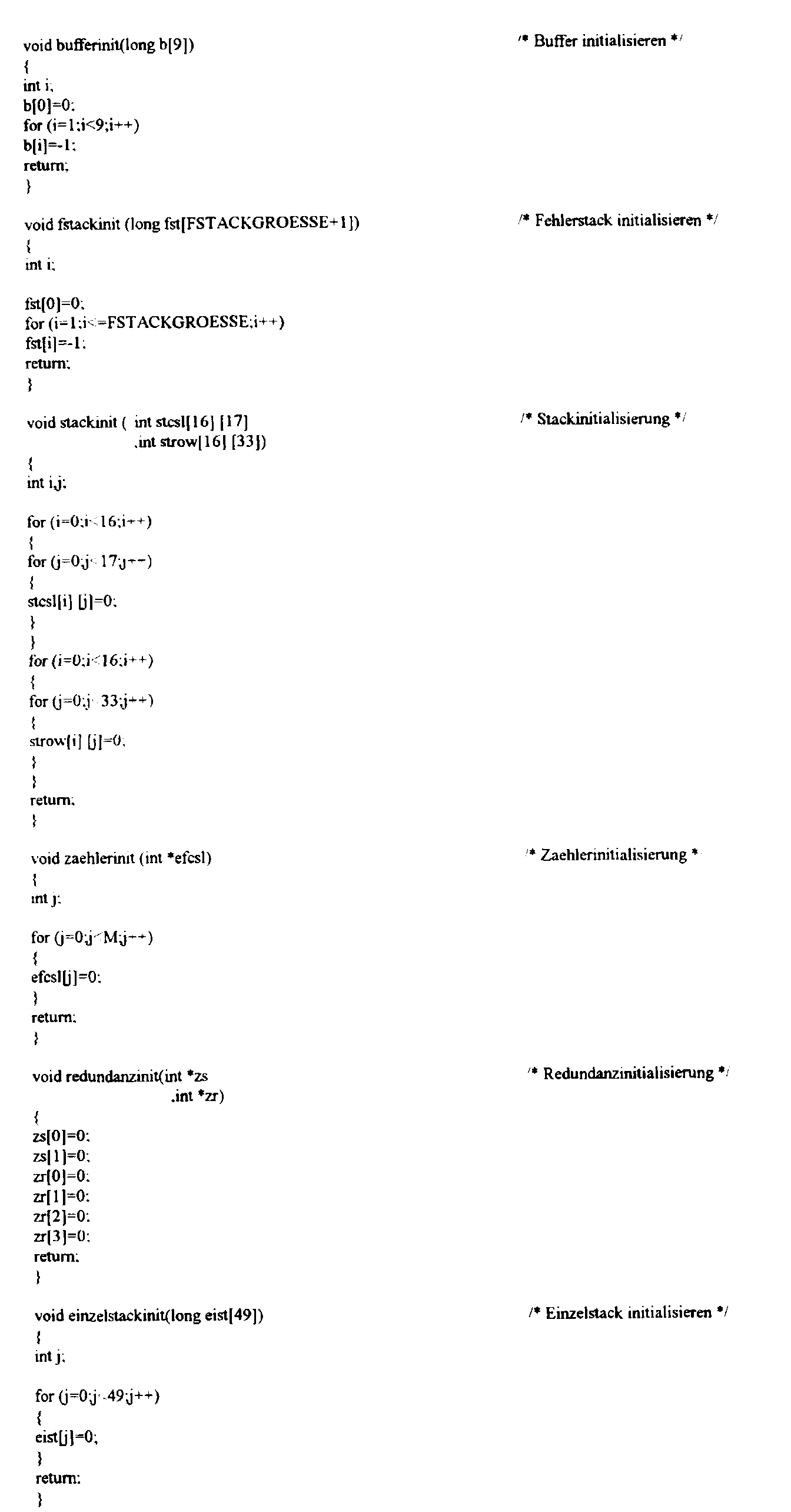
- the Memory array 1 has a plurality of word lines WL and a plurality of column select lines CSL and the content the memory field is compared with a comparator 21 compared to the registered test samples. Furthermore, the Comparator 21 a comparison of the error address in the form of Word line and column selection line with in corresponding Stack stores 41 and 42 stored error addresses. The error address determined in the comparator 21 is there Error counters 31 are available. In addition, in the Self-test device redundancy counter 32 is provided. values the error counter can be compared in a comparator 22 become.
- each word line has WL and each column selection line has its own error counter.
- all error counters are set to zero.
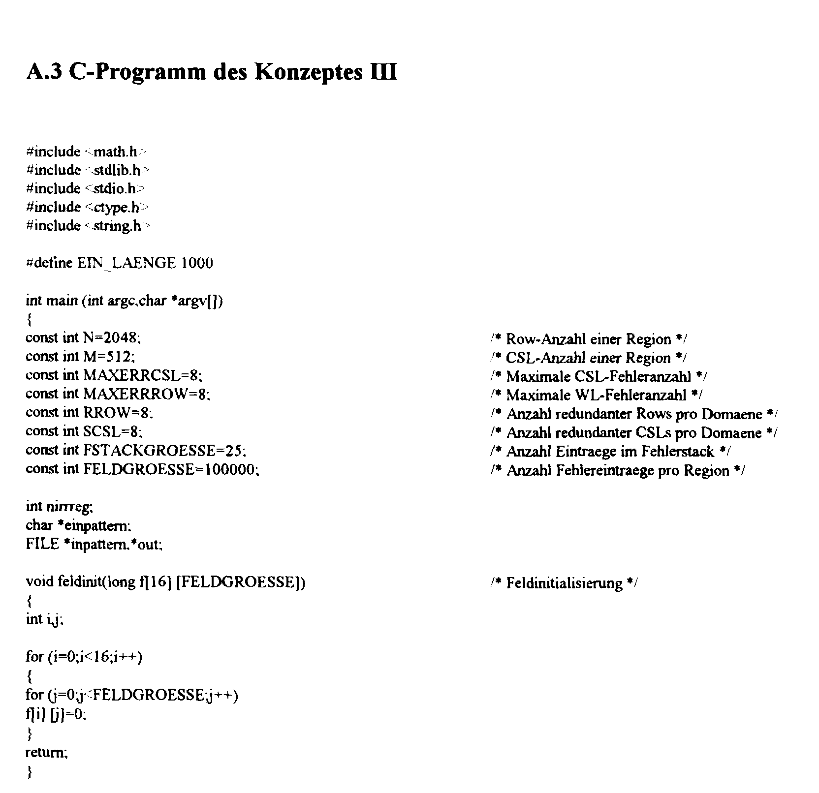
- the word and Column selection lines determined that a particularly large Show number of errors. It is used for the word lines and the Column selection lines an error number or a repair threshold set, in which the respective line by a accordingly redundant line should be replaced. The value this number depends on the memory chip to be tested, because different chips different redundancy organizations can own. An optimal choice of this repair threshold can be easier for the particular chip under test Way can be determined experimentally. The must also Space requirements of the architecture are taken into account.
- the repair threshold for the word lines can be different from that of the column select lines to be different.
- the error counters are e.g. B. advantageously dimensioned so that just in case of overflow reaches the limit is in which a line by a corresponding redundant Line should be replaced. That way can be very simply exceeding the remaining threshold due to an overflow bit.
- the memory field 1 represents one Storage region, which in turn consists of WL and CSL domains.
- the redundancy counters are advantageously designed so that that in the event of an overflow there is no suitable redundancy line there is more. So the memory chip is cannot be repaired and the test can be ended immediately in this case become.
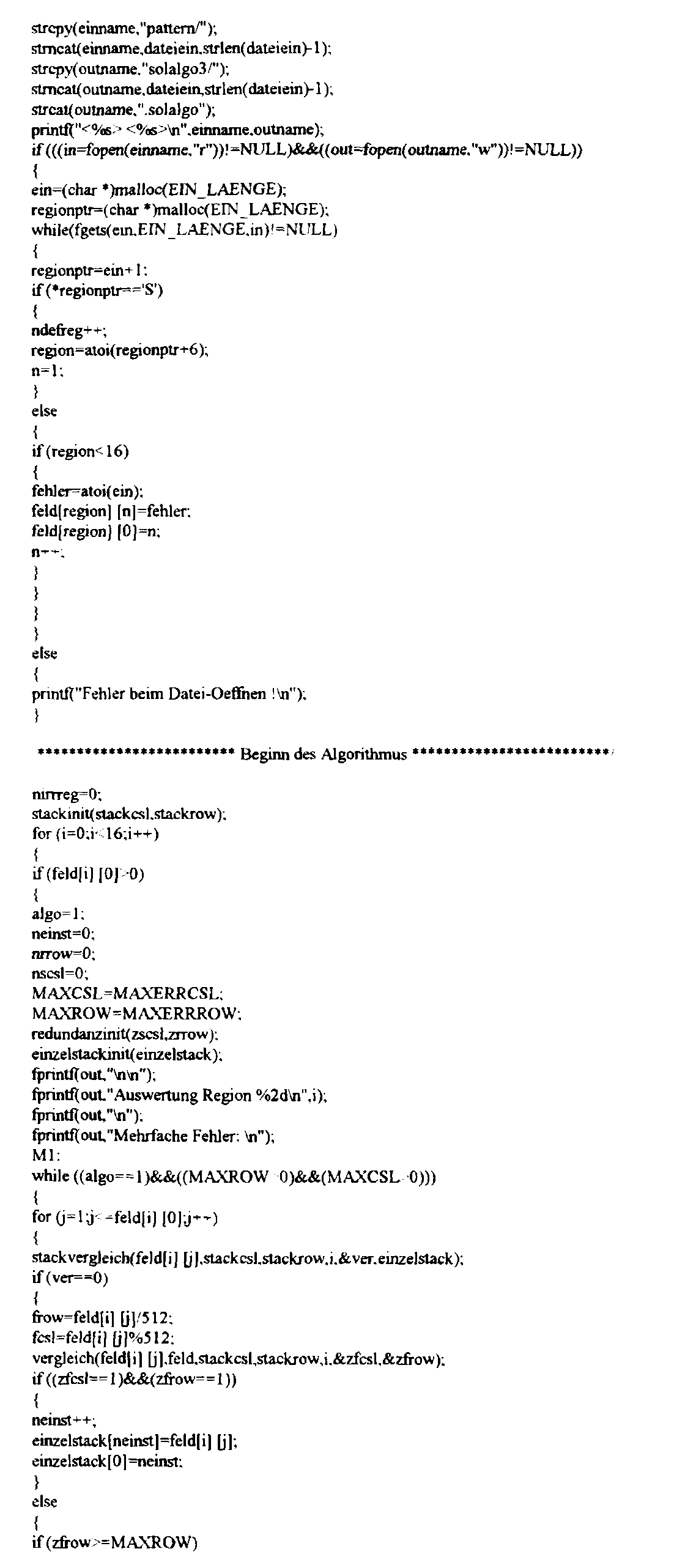
- the second part of the procedure begins.
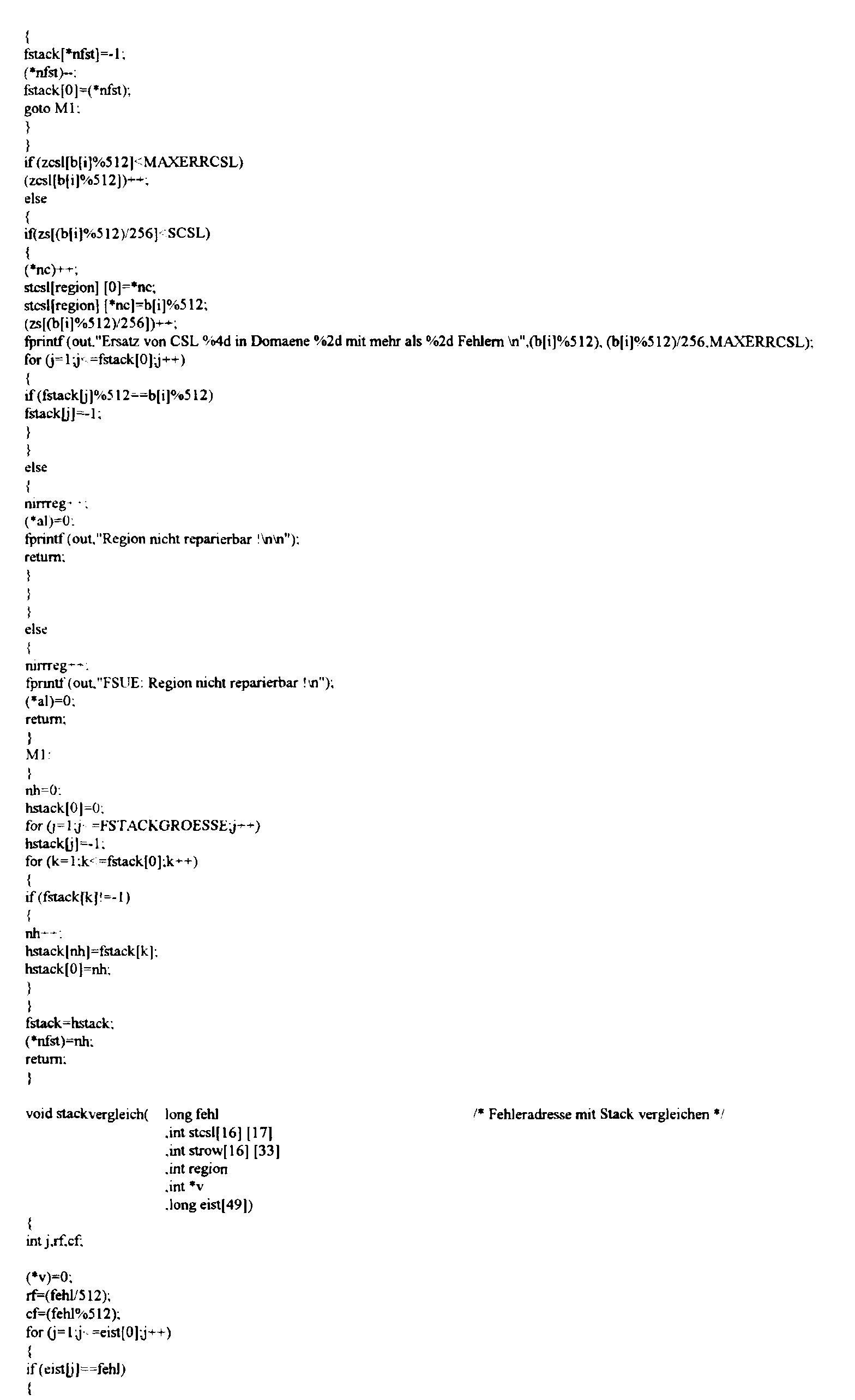
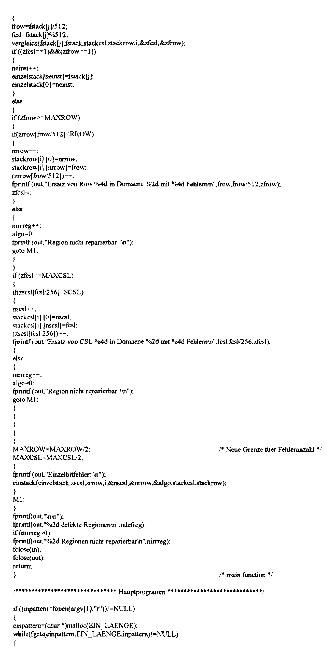
- the test patterns on the read / write memory are repeated created. With every test run, everyone Error counter set to zero. Now again the word line and column select line address becomes an error compared to the entries in the corresponding stack. Only if neither of the two addresses in the stack 41 and 42 is stored, the corresponding error counter 31 increased.
- the comparator is used 22 decided which address, word line or column selection line, is stored in the stack. This will first the word line and the column selection line with the largest number of errors determined. The values all error counters of the word lines WL and the error counters the column selection lines are compared separately, where the address of the word line and column selection line with most errors.
- Number of error counters can be reduced.
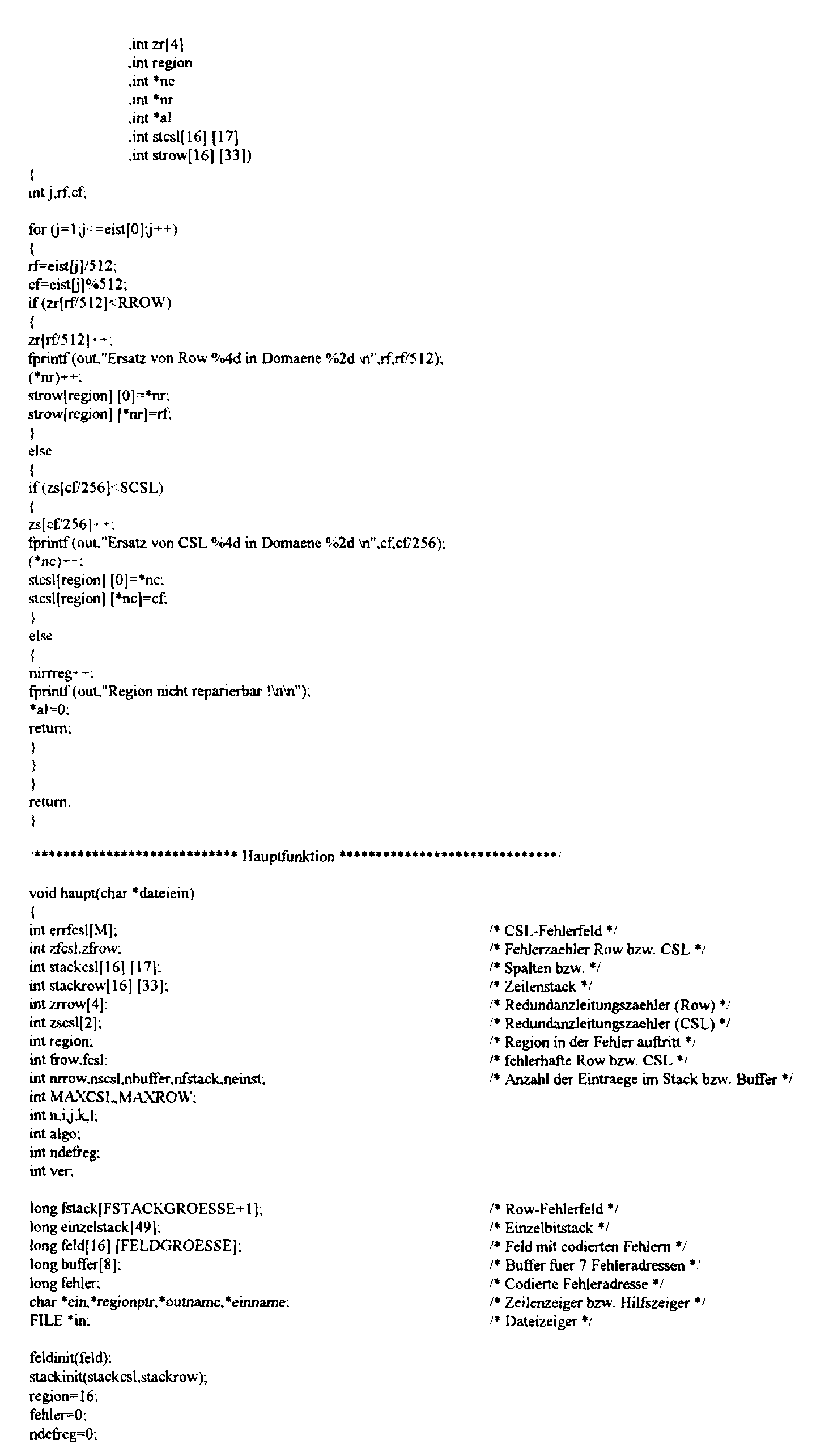
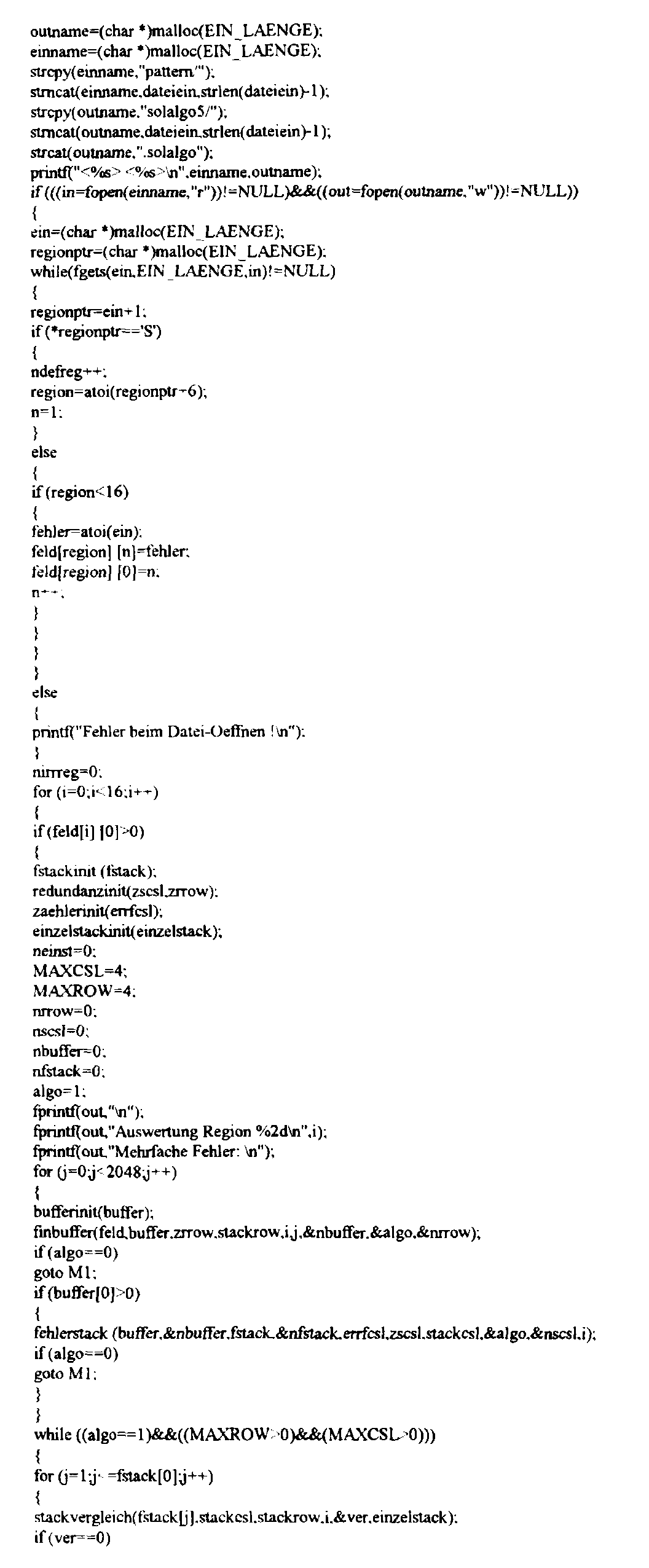
- the procedure will only slightly changed here. From reducing the The number of counters results in a longer test time since a longer one Number of test runs is necessary. Because if for everyone Word line and a counter for each column selection line can be repaired using the repair procedure described above a line to be repaired after a test run be determined. If there are fewer meters available, see above the number of test runs required increases. About one The error counter can switch a different group G of word lines and column select lines become. After each test run, the word line is then turned on and the column select line address with the most so far Errors, as well as the associated counter values in another Stack memory saved.
- Figure 2 is a second embodiment of the invention explained in more detail, with the representations essentially distinguish in that in addition an error stack 5 and a single bit stack 43 are present. In addition, it is indicated that the test procedure is interrupted must be and a changed test procedure must take place, if a faulty memory cell is discovered.
- This procedure also includes the selection of those to be repaired Lines require multiple test runs. This The method differs from the first embodiment by interrupting the test procedure with this concept must be recognized when an error is detected.
- the error address, the corresponding word line and column selection line address, is then stored in the error stack.
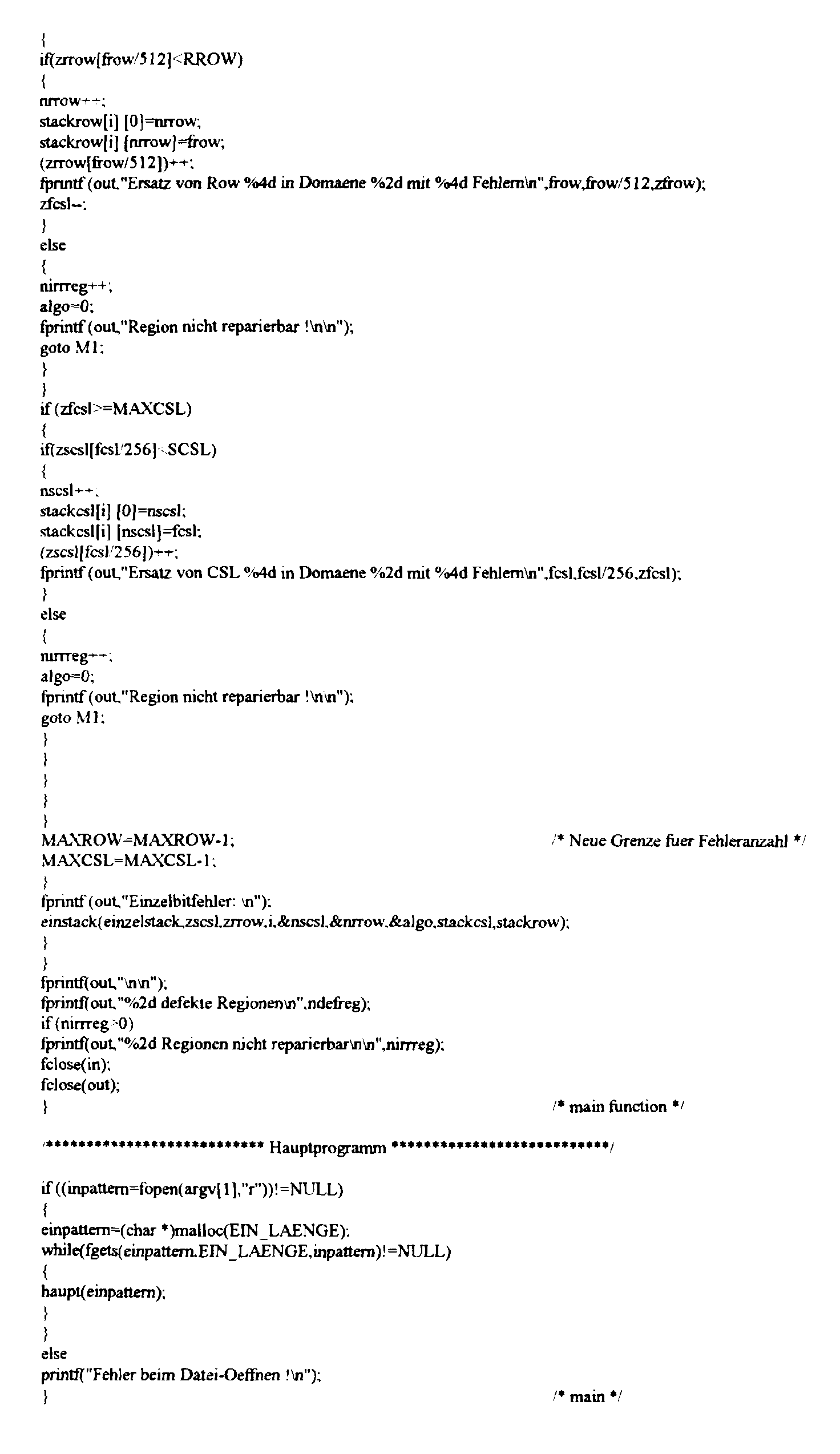
- the comparator 22 checks whether the error address is stored in one of the stack memories 41 ... 43 43 single-bit errors are stored in the memory become. If this is the case, the test procedure is carried out with another cell continued. Otherwise there is a changed one Test procedure. The number of all is shown separately Errors on the word line WL and on the column selection line CSL of the original error determined. Before counting the error must be checked whether the additional errors not just by activating a redundant line be resolved.
- the error counters must be set to zero beforehand become. Since the first comparison found that both the address of the word line and the address the column selection line of the original error is not stored in a stack, the following can Comparison process can be simplified. In the case of another Error on the word line of the original error must only the stack for the column select line addresses to be examined. An additional error occurs the column selection line of the original error, so only the stack must have the word line addresses with the Word line of the additional error can be compared. Exceeds the number of errors a certain limit, then the The address of the line is stored in the corresponding stack memory and the associated redundancy counter increases. The limit at that is to be repaired is in each subsequent test run reduced.
- FIG. 3 shows a block diagram to explain a third exemplary embodiment of the invention, which essentially differs from the block diagram in FIG. 2 by an additional buffer memory 6.
- the great advantage of this concept is that only a single test run is required to determine the word lines and column selection lines to be replaced. In addition, the test procedure does not have to be changed, which would have certain disadvantages.
- the error addresses of the respective word lines are stored in a buffer memory. If a certain number of errors is exceeded on this word line, the word line address is stored in the stack 41 and the contents of the buffer memory are deleted. In addition, the corresponding redundancy counter 32 must be increased.
- the entire contents of the buffer memory that is to say all the stored word line and column selection line addresses, are written into the error stack memory 5 and the buffer memory is then deleted.
- the size of the error stack 5 affects the test results.
- the error stack memory is processed while the next word line is being tested, that is to say the error addresses are determined and stored in the buffer memory.
- the column selection lines are determined and stored in the stack 42, which exceed a certain number of errors. For this purpose, the corresponding CSL error counters 31 are increased. With this architecture there is an error counter for each column selection line of the memory region to be tested. The error counters for the respective column selection lines are activated whenever new error addresses are written from the buffer memory into the error memory.
- the corresponding column selection line address is stored in the stack 42.
- the associated entries i.e. the column selection line address and the word line address, must be deleted from the error stack, since the errors are now repaired by using a redundant column selection line.
- the associated redundancy counter is also increased. This procedure ensures that even if a relatively small error stack memory is integrated, acceptable test results are achieved. If the fault stack memory overflows, it is not possible to repair the chip using this method and the built-in self-test can be stopped immediately at this point. After the test procedure has ended, the content of the error stack must be evaluated. For example, the method explained in the second exemplary embodiment can be used to evaluate the error stack memory.
Abstract
Description
Die Erfindung betrifft Vorrichtungen und Verfahren zum Testen von Schreib-/Lesespeichern mit integrierter Redundanz, bei denen Testmuster in einem Speicherfeld eingeschrieben und anschließend ausgelesen und verglichen werden sowie, wenn möglich, solange Wortleitungen und Spaltenauswahlleitungen durch redundante Leitungen ersetzt werden, bis keine Fehler mehr vorhanden sind.The invention relates to devices and methods for testing of read / write memories with integrated redundancy, at which test patterns are written into a memory field and then read out and compared and, if possible, as long as word lines and column selection lines redundant lines are replaced until no more errors available.
Bisher prüften auf dem Speicherchip integrierte Selbsttestarchitekturen nur, die Fehlerfreiheit des zugehörigen Chips. Eine Redundanzanalyse, bei der aus den Fehleradressen die zu ersetzenden Leitungen ermittelt werden, erfolgte hingegen bisher mit Hilfe eines externen Rechners, da bislang zunächst alle defekten Speicherzellen bestimmt und erst danach eine entsprechende Ersetzungsstrategie ermittelt wurde. Da ein derartiges Testverfahren unter anderem einen sehr großen Fehlerspeicher benötigt, ist dieses Verfahren nur mit einem externen Rechner sinnvoll durchführbar und kann praktisch nicht als eingebauter Selbsttest durchgeführt werden.So far, integrated self-test architectures have been testing on the memory chip only, the correctness of the associated chip. A redundancy analysis, in which the error addresses replacing lines are determined, however, was done so far with the help of an external computer, since so far initially determined all defective memory cells and only then one corresponding replacement strategy was determined. There a Such a test method, among other things, a very large error memory this procedure is only required with an external one Calculator can be carried out sensibly and practically cannot be carried out as a built-in self-test.
Die der Erfindung zugrundeliegende Aufgabe besteht nun darin, einen Schreib-/Lesespeicher mit einer integrierten Selbsttestvorrichtung und ein zugehöriges Testverfahren anzugeben, bei dem ein vollständiger Selbsttest inklusive der Redundanzanalyse ohne wesentliche externe Unterstützung durchführbar ist.The object on which the invention is based is now a read / write memory with an integrated self-test device and specify an associated test procedure in which a complete self-test including the redundancy analysis feasible without substantial external support is.
Die Erfindung wird nachfolgend anhand von in den Zeichnungen dargestellten Ausführungsbeispielen näher erläutert. Dabei zeigt
- Figur 1
- ein Blockdiagramm zur Erläuterung eines ersten Ausführungsbeispiels,
- Figur 2
- ein Blockdiagramm zur Erläuterung eines zweiten Ausführungsbeispiels und
Figur 3- ein Blockdiagramm zur Erläuterung eines dritten Ausführungsbeispiels.
- Figure 1
- 2 shows a block diagram to explain a first exemplary embodiment,
- Figure 2
- a block diagram for explaining a second embodiment and
- Figure 3
- a block diagram for explaining a third embodiment.
Die Erfindung besteht im wesentlichen darin, daß ein Schreib-/Lesespeicher mit einer auf dem Chip befindlichen Selbsttestvorrichtung ohne wesentliche externe Testeinrichtungen dadurch getestet werden kann, daß nicht zunächst alle Fehler ermittelt werden und dann erst eine Redundanzanalyse erfolgt, sondern daß zu reparierende Leitungen gespeichert und von weiteren Untersuchungen ausgeschlossen werden und immer die Leitungen mit den meisten noch nicht erfaßten fehlerhaften Speicherzellen solange durch Redundanzleitungen virtuell ersetzt werden, bis entweder keine redundanten Leitungen oder keine fehlerhaften Zellen mehr vorhanden sind.The invention essentially consists in the fact that a read / write memory with a self-test device on the chip without essential external test facilities can be tested that not all errors first are determined and only then is a redundancy analysis carried out, but that lines to be repaired and saved further examinations are excluded and always the Lines with the most faulty ones not yet recorded Memory cells are virtually replaced by redundancy lines until either no redundant lines or there are no more faulty cells.
Figur 1 zeigt eine schematische Darstellung einer im Speicherchip
integrierten Selbsttestarchitektur zur Reparatur eines
Speicherbausteins unter Einsatz der vorhandenen Leitungsredundanz.
Das Verfahren, das durch die Architektur realisiert
wird ist iterativ, das heißt, es benötigt zur Ermittlung
der zu aktivierenden Redundanzleitungen mehrere Testdurchläufe.
Ein Testdurchlauf beinhaltet alle Testmuster, die
für den entsprechenden Speicherchip während des sogenannten
Prefuse-Tests vorgesehen sind. Von einer Steuereinheit CTRL
die beispielsweise einen Nurlesespeicher ROM enthält, sind
Testmuster in ein Speicherfeld einlesbar. Das Speicherfeld 1
entspricht hier einer Region eines Gesamtspeicherfeldes, dem
eine gewisse Anzahl von redundanten Leitungen zugeordnet
sind. Die Steuereinheit CTRL übernimmt die gesamte Ablaufsteuerung
und kann mit externen Daten versorgt werden. Das
Speicherfeld 1 weist eine Mehrzahl von Wortleitungen WL und
eine Mehrzahl von Spaltenauswahlleitungen CSL auf und der Inhalt
des Speicherfeldes wird durch einen Vergleicher 21 mit
den eingeschriebenen Testmustern verglichen. Ferner führt der
Vergleicher 21 einen Vergleich der Fehleradresse in Form von
Wortleitung und Spaltenauswahlleitung mit in entsprechenden
Stapelspeichern 41 und 42 gespeicherten Fehleradressen durch.
Die im Vergleicher 21 festgestellte Fehleradresse steht
Fehlerzählern 31 zur Verfügung. Darüber hinaus sind in der
Selbsttestvorrichtung Redundanzzähler 32 vorgesehen. Werte
der Fehlerzähler können in einem Vergleicher 22 verglichen
werden.Figure 1 shows a schematic representation of a in the memory chip
integrated self test architecture to repair a
Memory module using the existing line redundancy.
The process realized through architecture
is iterative, that is, it needs to be determined
of the redundancy lines to be activated several test runs.
A test run includes all test patterns that
for the corresponding memory chip during the so-called
Prefuse tests are provided. From a control unit CTRL
which contains, for example, a read-only memory ROM
Test pattern can be read into a memory field. The storage field 1
corresponds here to a region of a total storage field, the
assigned a certain number of redundant lines
are. The control unit CTRL takes over the entire process control
and can be supplied with external data. The
Memory array 1 has a plurality of word lines WL and
a plurality of column select lines CSL and the content
the memory field is compared with a
In diesem Ausführungsbeispiel besitzt jede Wortleitung WL und jede Spaltenauswahlleitung einen eigenen Fehlerzähler. Zu Beginn des Testablaufs werden alle Fehlerzähler auf Null gesetzt. Während des ersten Testdurchlaufs werden die Wort- und Spaltenauswahlleitungen ermittelt, die eine besonders große Fehleranzahl aufweisen. Es wird für die Wortleitungen und die Spaltenauswahlleitungen eine Fehlerzahl bzw. eine Reparaturschwelle festgelegt, bei der die jeweilige Leitung durch eine entsprechend redundante Leitung ersetzt werden soll. Der Wert dieser Zahl ist vom zu testenden Speicherbaustein abhängig, da verschiedene Chips unterschiedliche Redundanzorganisationen besitzen können. Eine optimale Wahl dieser Reparaturschwelle kann für den jeweiligen zu testenden Chip in einfacher Weise experimentell ermittelt werden. Dabei muß auch der Flächenbedarf der Architektur berücksichtigt werden. Die Reparaturschwelle für die Wortleitungen kann von der der Spaltenauswahlleitungen verschieden sein.In this embodiment, each word line has WL and each column selection line has its own error counter. At the start of the test procedure, all error counters are set to zero. During the first test run, the word and Column selection lines determined that a particularly large Show number of errors. It is used for the word lines and the Column selection lines an error number or a repair threshold set, in which the respective line by a accordingly redundant line should be replaced. The value this number depends on the memory chip to be tested, because different chips different redundancy organizations can own. An optimal choice of this repair threshold can be easier for the particular chip under test Way can be determined experimentally. The must also Space requirements of the architecture are taken into account. The repair threshold for the word lines can be different from that of the column select lines to be different.
Die Fehlerzähler werden z. B. vorteilhafterweise so dimensioniert, daß gerade im Falle des Überlaufs die Grenze erreicht wird, bei der eine Leitung durch eine entsprechende redundante Leitung ersetzt werden soll. Auf diese Weise kann sehr einfach das Überschreiten der verbliebenen Schwelle aufgrund eines Überlaufbits erfolgen. The error counters are e.g. B. advantageously dimensioned so that just in case of overflow reaches the limit is in which a line by a corresponding redundant Line should be replaced. That way can be very simply exceeding the remaining threshold due to an overflow bit.
Bevor die jeweiligen Fehlerzähler einer defekten Leitung erhöht
werden, muß überprüft werden, ob die Wortleitungs- oder
Spaltenauswahlleitungsadresse des Fehlers schon im zugehörigen
Stapelspeicher abgelegt ist. In diesem Fall werden die
Zähler nicht aktiviert, da der Fehler schon repariert wird.
Dieser Vergleich muß schon im ersten Testdurchlauf erfolgen,
weil ein Durchlauf aus mehreren Testmustern besteht. Dadurch
wird vermieden, daß ein Fehler durch mehrere redundante Leitungen
behoben wird. Die Adressen der Leitungen, deren
Fehlerzähler nach dem ersten Testdurchlauf übergelaufen sind
werden im Wortleitungsstapelspeicher 41 bzw. im Spaltenauswahlleitungsstapelspeicher
42 abgespeichert. Außerdem werden
die zugehörigen Redundanzzähler 32 erhöht. Dazu muß die Domäne
der zu ersetzenden Leitung bestimmt werden, denn es gibt
üblicherweise für jede Wortleitungs- und für jede Spaltenauswahlleitungsdomäne
eines Speicherchips eine fest vorgegebene
Zahl an Redundanzleitungen. Das Speicherfeld 1 stellt eine
Speicherregion dar, die wiederum aus WL- und CSL-Domänen besteht.
Die Redundanzzähler sind vorteilhafterweise so ausgelegt,
daß im Falle eines Überlaufs keine passende Redundanzleitung
mehr vorhanden ist. Der Speicherbaustein ist also
nicht reparierbar und der Test kann in diesem Fall sofort beendet
werden.Before the respective error counter of a defective line increases
must be checked whether the word line or
Column selection line address of the error already in the associated
Stack memory is stored. In this case, the
Counter not activated because the error is already being repaired.
This comparison has to be done in the first test run,
because a run consists of several test patterns. Thereby
it is avoided that an error is caused by several redundant lines
is fixed. The addresses of the lines whose
Error counters overflowed after the first test run
are in the
Nachdem alle Testmuster einmal in den Schreib-/Lesespeicher
eingeschrieben wurden, beginnt der zweite Teil des Verfahrens.
Wiederholt werden die Testmuster an den Schreib-/Lesespeicher
angelegt. Bei jedem Testdurchlauf werden alle
Fehlerzähler auf Null gesetzt. Nun wird wiederum die Wortleitungs- und Spaltenauswahlleitungsadresse eines Fehlers mit
den Einträgen der entsprechenden Stapelspeicher verglichen.
Nur wenn keine der beiden Adressen in dem Stapelspeicher 41
und 42 abgelegt ist, werden die entsprechenden Fehlerzähler
31 erhöht. Nach einem Durchlauf wird mit Hilfe des Vergleichers
22 entschieden, welche Adresse, Wortleitung oder Spaltenauswahlleitung,
im Stapelspeicher abgelegt wird. Dazu wird
zunächst die Wortleitung und die Spaltenauswahlleitung mit
der größten Fehleranzahl ermittelt. Dabei werden die Werte
aller Fehlerzähler der Wortleitungen WL und die Fehlerzähler
der Spaltenauswahlleitungen separat miteinander verglichen,
wobei die Adresse der Wortleitung und der Spaltenauswahlleitung
mit den meisten Fehlern ermittelt wird. Anschließend
werden diese beiden Werte miteinander verglichen. Aus dem
Vergleich geht hervor, welche der beiden Leitungen, also entweder
die Wortleitung oder die Spaltenauswahlleitung, repariert
werden soll. Existiert noch eine entsprechende Redundanzleitung
in der betreffenden Domäne, ist also der Redundanzzähler
dieser Domäne noch nicht übergelaufen, so wird die
Adresse im Stapelspeicher abgelegt und der Redundanzzähler
erhöht. Ansonsten wird die Adresse des anderen Maximums im
Stapelspeicher gespeichert. Nur wenn auch für diese Leitung
keine Redundanz mehr vorhanden ist, handelt es sich um einen
irreparablen Speicherchip und der eingebaute Selbsttest kann
abgebrochen werden. Beendet ist der Test, wenn der Speicherchip
entweder keine Fehler mehr besitzt, daß heißt, daß alle
Fehlerzähler nach einem Testdurchlauf auf Null sind, oder
wenn keine passenden Redundanzleitungen vorhanden sind, also
ein Redundanzzähler überläuft. Die Adressen der Leitungen,
die ersetzt werden sollen, befinden sich nach einem vollständigen
Testablauf in den Stapelspeichern 41 und 42. Dies sind
sogenannte Fuse-Informationen, die der Laser benötigt, um den
Chip mit der vorhandenen Redundanz reparieren zu können.After all test patterns once in the read / write memory
the second part of the procedure begins.
The test patterns on the read / write memory are repeated
created. With every test run, everyone
Error counter set to zero. Now again the word line and column select line address becomes an error
compared to the entries in the corresponding stack.
Only if neither of the two addresses in the
Um den Flächenbedarf dieser eingebauten Selbsttestarchitektur zu verringern, kann in einer vorteilhaften Ausgestaltung die Anzahl der Fehlerzähler reduziert werden. Das Verfahren wird hierbei nur unwesentlich verändert. Aus der Verringerung der Zähleranzahl resultiert eine höhere Testzeit, da eine größere Anzahl an Testdurchläufen notwendig ist. Denn wenn für jede Wortleitung und für jede Spaltenauswahlleitung ein Zähler vorhanden ist, kann mit dem oben beschriebenen Reparaturverfahren nach einem Testdurchlauf eine zu reparierende Leitung bestimmt werden. Stehen weniger Zähler zur Verfügung, so steigt die Anzahl der erforderlichen Testdurchläufe. Über einen Schalter kann den Fehlerzähler jeweils eine andere Gruppe G von Wortleitungen und Spaltenauswahlleitungen zugeordnet werden. Nach jedem Testdurchlauf wird dann die Wortleitung und die Spaltenauswahlleitungsadresse mit den bis dahin meisten Fehlern, sowie die zugehörigen Zählerwerte in einem weiteren Stapelspeicher abgespeichert. Dazu müssen alle neuen Zählerwerte mit dem bisherigen Maximalwert, welcher in einem Stapelspeicher abgelegt ist, verglichen werden. Dies erfolgt sowohl für die Wortleitungen als auch für die Spaltenauswahlleitungen. Danach werden die Zähler der nächsten Gruppe von Leitungen zugeordnet und es werden die Fehler auf diesen Leitungen gezählt.The space requirements of this built-in self-test architecture to reduce, can in an advantageous embodiment Number of error counters can be reduced. The procedure will only slightly changed here. From reducing the The number of counters results in a longer test time since a longer one Number of test runs is necessary. Because if for everyone Word line and a counter for each column selection line can be repaired using the repair procedure described above a line to be repaired after a test run be determined. If there are fewer meters available, see above the number of test runs required increases. About one The error counter can switch a different group G of word lines and column select lines become. After each test run, the word line is then turned on and the column select line address with the most so far Errors, as well as the associated counter values in another Stack memory saved. To do this, all new ones Counter values with the previous maximum value, which in one Stack memory is stored, are compared. this happens for both the word lines and the column select lines. Then the counters of the next group of Lines are assigned and there are errors on these lines counted.
In Figur 2 ist ein zweites Ausführungsbeispiel der Erfindung
näher erläutert, wobei sich die Darstellungen im wesentlichen
dadurch unterscheiden, daß zusätzlich ein Fehlerstapelspeicher
5 und ein Einzelbitstapelspeicher 43 vorhanden sind.
Darüber hinaus ist angedeutet, daß der Testablauf unterbrochen
werden muß und ein veränderter Testablauf erfolgen muß,
wenn eine fehlerhafte Speicherzelle entdeckt wird.In Figure 2 is a second embodiment of the invention
explained in more detail, with the representations essentially
distinguish in that in addition an error stack
5 and a
Auch bei diesem Verfahren sind zur Auswahl der zu reparierenden
Leitungen mehrere Testdurchläufe erforderlich. Dieses
Verfahren unterscheidet sich von dem ersten Ausführungsbeispiel
dadurch, daß der Testablauf bei diesem Konzept unterbrochen
werden muß, wenn ein Fehler erkannt wird. Die Fehleradresse,
also die entsprechende Wortleitungs- und Spaltenauswahlleitungsadresse,
wird dann im Fehlerstapelspeicher abgespeichert.
Der Vergleicher 22 überprüft anschließend, ob
die Fehleradresse in einem der Stapelspeicher 41 ... 43 gespeichert
ist, wobei im Speicher 43 Einzelbitfehler gespeichert
werden. Ist dies der Fall, so wird der Testablauf mit
einer anderen Zelle fortgesetzt. Ansonsten folgt ein veränderter
Testablauf. Es wird hierbei separat die Anzahl aller
Fehler auf der Wortleitung WL und auf der Spaltenauswahlleitung
CSL des ursprünglichen Fehlers ermittelt. Vor dem Zählen
der Fehler muß überprüft werden, ob die zusätzlichen Fehler
nicht schon durch das Aktivieren einer redundanten Leitung
behoben werden. Zuvor müssen die Fehlerzähler auf Null gesetzt
werden. Da beim ersten Vergleich festgestellt wurde,
daß sowohl die Adresse der Wortleitung als auch die Adresse
der Spaltenauswahlleitung des ursprünglichen Fehlers noch
nicht in einem Stapelspeicher abgelegt ist, kann der folgende
Vergleichsvorgang vereinfacht werden. Im Falle eines weiteren
Fehlers auf der Wortleitung des ursprünglichen Fehlers muß
lediglich der Stapelspeicher für die Spaltenauswahlleitungsadressen
untersucht werden. Tritt ein zusätzlicher Fehler auf
der Spaltenauswahlleitung des ursprünglichen Fehlers auf, so
muß nur der Stapelspeicher die Wortleitungsadressen mit der
Wortleitung des zusätzlichen Fehlers verglichen werden. Übersteigt
die Fehleranzahl eine bestimmte Grenze, so wird die
Adresse der Leitung im entsprechenden Stapelspeicher abgelegt
und der zugehörige Redundanzzähler erhöht. Die Grenze, bei
der repariert werden soll, wird in jedem folgenden Testdurchlauf
herabgesetzt.This procedure also includes the selection of those to be repaired
Lines require multiple test runs. This
The method differs from the first embodiment
by interrupting the test procedure with this concept
must be recognized when an error is detected. The error address,
the corresponding word line and column selection line address,
is then stored in the error stack.
The
Dies kann vorteilhafterweise dadurch geschehen, daß die unterschiedlichen Grenzen durch Zähler mit unterschiedlicher Wortbreite festgelegt werden. Beim Überlauf der jeweiligen Zähler wird diese Grenze erreicht. So können beispielsweise im ersten Testdurchlauf zwei Drei-Bit-Zähler verwendet werden. Dadurch würden dann in diesem Durchgang die Adressen der Leitungen abgespeichert, die mehr als sieben Fehler aufweisen. Im nächsten Testdurchlauf könnten zwei Zwei-Bit-Zähler zum Einsatz kommen, so daß die Grenze für eine erforderliche Reparatur von acht auf vier herabgesetzt wird. Im folgenden Testdurchgang können zwei Ein-Bit-Zähler benutzt werden. Die Aktivierung der verschiedenen Zähler erfolgt über Befehle, die beispielsweise im Speicher ROM der Steuereinheit gespeichert sind. Die Anzahl und die Dimensionierung der Zähler richtet sich nach dem zu testenden Speicherchip.This can advantageously be done in that the different Limits through counters with different Word width can be set. When the respective overflow This limit is reached. For example two three-bit counters are used in the first test run. The addresses of the Lines stored that have more than seven errors. In the next test run, two two-bit counters could be used be used so that the limit for a required Repair is reduced from eight to four. Hereinafter Two single-bit counters can be used for the test run. The The various counters are activated via commands, which are stored, for example, in the ROM of the control unit are. The number and dimensioning of the counters depends on the memory chip to be tested.
Durch die Anzahl der verwendeten Fehlerzähler wird auch die
Zahl der erforderlichen Testdurchläufe vorgegeben. Gibt es
keine weiteren Fehler auf der Wortleitung WL und der Spaltenauswahlleitung
CSL des ursprünglichen Fehlers, so handelt es
sich um einen Einzelbitfehler, dessen Adresse im Stapelspeicher
43 gespeichert wird. In ihm wird die komplette Adresse,
also die Wortleitungs- und die Spaltenauswahlleitungsadresse
abgespeichert. Am Ende des eingebauten Selbsttests wird dieser
Stapelspeicher bearbeitet. Die Fehler, die dort gespeichert
sind, können sowohl durch eine redundante Wortleitung
als auch durch eine redundante Spaltenauswahlleitung ersetzt
werden. Da die redundanten Wortleitungen meist anders organisiert
sind als die redundanten Spaltenauswahlleitungen, unterscheiden
sich die Testergebnisse, je nachdem mit welchen
Redundanzleitungen die Einzelbitfehler behoben werden. Beendet
ist der komplette Testablauf, wenn keine benötigten Redundanzleitungen
mehr vorhanden sind, oder alle Fehler behoben
sind. Läuft einer der Redundanzzähler über, so ist der Speicherchip
nicht reparierbar und der Test kann sofort abgebrochen
werden. Die vollständige Reparatur des Chips wird dadurch
erkannt, daß während eines gesamten Testdurchgangs die
Zähler immer auf Null stehenbleiben. Sobald ein Fehlerzähler
erhöht wird, so besitzt der Chip noch mindestens einen Fehler
und der Testablauf kann in diesem Fall nicht beendet werden.Due to the number of error counters used, the
Number of test runs required. Is there
no further errors on the word line WL and the column selection line
CSL of the original error, so do it
is a single bit error whose address is in the
In Figur 3 ist ein Blockdiagramm zur Erläuterung eines dritten
Ausführungsbeispiels der Erfindung dargestellt, das sich
im wesentlichen durch einen zusätzlichen Pufferspeicher 6 vom
Blockdiagramm in Figur 2 unterscheidet. Der große Vorteil
dieses Konzeptes besteht darin, daß nur ein einziger Testdurchlauf
zur Bestimmung der zu ersetzenden Wortleitungen und
Spaltenauswahlleitungen benötigt wird. Außerdem muß der Testablauf
nicht abgeändert werden, was gewisse Nachteile mit
sich bringen würde. Die Fehleradressen der jeweiligen Wortleitung
werden in einem Pufferspeicher abgespeichert. Wird
eine bestimmte Fehleranzahl auf dieser Wortleitung überschritten,
so wird die Wortleitungsadresse im Stapelspeicher
41 abgelegt und der Inhalt des Pufferspeichers gelöscht. Außerdem
muß der entsprechende Redundanzzähler 32 erhöht werden.
Besitzt die Wortleitung weniger Fehler als die festgelegte
Fehleranzahl, so wird der komplette Inhalt des Pufferspeichers,
also alle gespeicherten Wortleitungs- und Spaltenauswahlleitungsadressen
in den Fehlerstapelspeicher 5 eingeschrieben
und anschließend der Pufferspeicher gelöscht. Die
Größe des Fehlerstapelspeichers 5 beeinflußt die Testergebnisse.
Während die nächste Wortleitung getestet wird, das
heißt, die Fehleradressen bestimmt und in dem Pufferspeicher
abgespeichert werden, erfolgt die Bearbeitung des Fehlerstapelspeichers.
Es werden die Spaltenauswahlleitungen ermittelt
und im Stapelspeicher 42 abgespeichert, die eine gewisse Fehleranzahl
übertreffen. Dazu werden die entsprechenden CSL-Fehlerzähler
31 erhöht. Es gibt bei dieser Architektur für
jede Spaltenauswahlleitung der zu testenden Speicherregion
einen Fehlerzähler. Die Fehlerzähler für die jeweiligen Spaltenauswahlleitungen
werden immer dann aktiviert, wenn neue
Fehleradressen vom Pufferspeicher in den Fehlerspeicher eingeschrieben
werden. Läuft einer dieser Fehlerzähler über, so
wird die entsprechende Spaltenauswahlleitungsadresse im Stapelspeicher
42 abgespeichert. Außerdem müssen die zugehörigen
Einträge, also die Spaltenauswahlleitungsadresse und die
Wortleitungsadresse, aus dem Fehlerstapelspeicher gelöscht
werden, da die Fehler nun durch den Einsatz einer redundanten
Spaltenauswahlleitung repariert werden. Zudem wird der zugehörige
Redundanzzähler erhöht. Diese Vorgehensweise sorgt dafür,
daß auch bei Integration eines relativ kleinen Fehlerstapelspeichers
schon akzeptable Testergebnisse erzielt werden.
Läuft der Fehlerstapelspeicher über, so ist eine Reparatur
des Chips mit Hilfe dieses Verfahrens nicht möglich und
der eingebaute Selbsttest kann an dieser Stelle sofort abgebrochen
werden. Nachdem der Testablauf beendet ist, muß der
Inhalt des Fehlerstapelspeichers ausgewertet werden. Zur Auswertung
des Fehlerstapelspeichers kann beispielsweise das im
zweiten Ausführungsbeispiel erläuterte Verfahren verwendet
werden.
![]()


![]()
Claims (11)
Applications Claiming Priority (2)
| Application Number | Priority Date | Filing Date | Title |
|---|---|---|---|
| DE19850115 | 1998-10-30 | ||
| DE19850115 | 1998-10-30 |
Publications (3)
| Publication Number | Publication Date |
|---|---|
| EP1008993A2 true EP1008993A2 (en) | 2000-06-14 |
| EP1008993A3 EP1008993A3 (en) | 2005-05-11 |
| EP1008993B1 EP1008993B1 (en) | 2007-07-18 |
Family
ID=7886194
Family Applications (1)
| Application Number | Title | Priority Date | Filing Date |
|---|---|---|---|
| EP99121604A Expired - Lifetime EP1008993B1 (en) | 1998-10-30 | 1999-10-29 | Writeable memory with self-test device and method therefor |
Country Status (4)
| Country | Link |
|---|---|
| US (1) | US6539506B1 (en) |
| EP (1) | EP1008993B1 (en) |
| DE (1) | DE59914414D1 (en) |
| TW (1) | TW446955B (en) |
Cited By (2)
| Publication number | Priority date | Publication date | Assignee | Title |
|---|---|---|---|---|
| WO2005015568A1 (en) * | 2003-07-21 | 2005-02-17 | Infineon Technologies Ag | Memory device and method of storing fail addresses of a memory cell |
| EP1465204A3 (en) * | 2003-02-12 | 2005-03-30 | Infineon Technologies AG | Memory built-in self repair (MBISR) circuits / devices |
Families Citing this family (16)
| Publication number | Priority date | Publication date | Assignee | Title |
|---|---|---|---|---|
| US6725403B1 (en) * | 1999-11-02 | 2004-04-20 | Infineon Technologies Richmond, Lp | Efficient redundancy calculation system and method for various types of memory devices |
| US6795942B1 (en) * | 2000-07-06 | 2004-09-21 | Lsi Logic Corporation | Built-in redundancy analysis for memories with row and column repair |
| JP2002343098A (en) * | 2001-05-18 | 2002-11-29 | Mitsubishi Electric Corp | Test method for semiconductor memory |
| JP4137474B2 (en) * | 2002-03-18 | 2008-08-20 | 富士通株式会社 | Self-test circuit and semiconductor memory device |
| US7065723B2 (en) * | 2002-09-25 | 2006-06-20 | Sun Microsystems, Inc. | Defect tracking by utilizing real-time counters in network computing environments |
| DE102004022327B4 (en) * | 2004-05-06 | 2006-04-27 | Infineon Technologies Ag | Integrated semiconductor memory |
| JP4472424B2 (en) * | 2004-05-17 | 2010-06-02 | 富士通マイクロエレクトロニクス株式会社 | Netlist generation method and computer program thereof |
| US8412985B1 (en) | 2009-06-30 | 2013-04-02 | Micron Technology, Inc. | Hardwired remapped memory |
| US8412987B2 (en) * | 2009-06-30 | 2013-04-02 | Micron Technology, Inc. | Non-volatile memory to store memory remap information |
| US20100332894A1 (en) * | 2009-06-30 | 2010-12-30 | Stephen Bowers | Bit error threshold and remapping a memory device |
| US8495467B1 (en) | 2009-06-30 | 2013-07-23 | Micron Technology, Inc. | Switchable on-die memory error correcting engine |
| US8347154B2 (en) * | 2010-09-21 | 2013-01-01 | International Business Machines Corporation | Use of hashing function to distinguish random and repeat errors in a memory system |
| US10073685B2 (en) * | 2015-01-19 | 2018-09-11 | SK Hynix Inc. | Methods of system optimization by over-sampling read |
| KR20180104455A (en) * | 2017-03-13 | 2018-09-21 | 에스케이하이닉스 주식회사 | Repair device and semiconductor including the same |
| KR20240004062A (en) * | 2022-07-04 | 2024-01-11 | 삼성전자주식회사 | Operation method of memory device, semiconductor device and test method of memory device |
| CN116486882B (en) * | 2023-04-27 | 2023-12-08 | 深圳市晶存科技有限公司 | Method, device, equipment and medium for testing chip performance based on word line |
Citations (3)
| Publication number | Priority date | Publication date | Assignee | Title |
|---|---|---|---|---|
| US4493075A (en) * | 1982-05-17 | 1985-01-08 | National Semiconductor Corporation | Self repairing bulk memory |
| US5278839A (en) * | 1990-04-18 | 1994-01-11 | Hitachi, Ltd. | Semiconductor integrated circuit having self-check and self-repair capabilities |
| US5764878A (en) * | 1996-02-07 | 1998-06-09 | Lsi Logic Corporation | Built-in self repair system for embedded memories |
Family Cites Families (4)
| Publication number | Priority date | Publication date | Assignee | Title |
|---|---|---|---|---|
| US3845476A (en) * | 1972-12-29 | 1974-10-29 | Ibm | Monolithic memory using partially defective chips |
| US4456995A (en) * | 1981-12-18 | 1984-06-26 | International Business Machines Corporation | Apparatus for high speed fault mapping of large memories |
| JP2777276B2 (en) * | 1990-09-20 | 1998-07-16 | 株式会社東芝 | Test device for memory IC with redundant circuit |
| DE9412376U1 (en) | 1994-08-01 | 1995-12-07 | Telbus Ges Fuer Elektronische | Memory circuit to compensate for bit errors in memory modules |
-
1999
- 1999-10-27 TW TW088118567A patent/TW446955B/en not_active IP Right Cessation
- 1999-10-29 DE DE59914414T patent/DE59914414D1/en not_active Expired - Fee Related
- 1999-10-29 EP EP99121604A patent/EP1008993B1/en not_active Expired - Lifetime
- 1999-11-01 US US09/431,529 patent/US6539506B1/en not_active Expired - Lifetime
Patent Citations (3)
| Publication number | Priority date | Publication date | Assignee | Title |
|---|---|---|---|---|
| US4493075A (en) * | 1982-05-17 | 1985-01-08 | National Semiconductor Corporation | Self repairing bulk memory |
| US5278839A (en) * | 1990-04-18 | 1994-01-11 | Hitachi, Ltd. | Semiconductor integrated circuit having self-check and self-repair capabilities |
| US5764878A (en) * | 1996-02-07 | 1998-06-09 | Lsi Logic Corporation | Built-in self repair system for embedded memories |
Cited By (4)
| Publication number | Priority date | Publication date | Assignee | Title |
|---|---|---|---|---|
| EP1465204A3 (en) * | 2003-02-12 | 2005-03-30 | Infineon Technologies AG | Memory built-in self repair (MBISR) circuits / devices |
| WO2005015568A1 (en) * | 2003-07-21 | 2005-02-17 | Infineon Technologies Ag | Memory device and method of storing fail addresses of a memory cell |
| US6937531B2 (en) | 2003-07-21 | 2005-08-30 | Infineon Technologies Ag | Memory device and method of storing fail addresses of a memory cell |
| KR100760052B1 (en) * | 2003-07-21 | 2007-09-18 | 인피니언 테크놀로지스 아게 | Memory device and method of storing fail addresses of a memory cell |
Also Published As
| Publication number | Publication date |
|---|---|
| DE59914414D1 (en) | 2007-08-30 |
| US6539506B1 (en) | 2003-03-25 |
| TW446955B (en) | 2001-07-21 |
| EP1008993B1 (en) | 2007-07-18 |
| EP1008993A3 (en) | 2005-05-11 |
Similar Documents
| Publication | Publication Date | Title |
|---|---|---|
| EP1008993A2 (en) | Writeable memory with self-test device and method therefor | |
| EP0378538B1 (en) | Arrangement and process for detecting and localizing faulty circuits in a storage component | |
| DE10225381A1 (en) | Method and device for storing memory test information | |
| EP0046976A2 (en) | Semi-conductor memory made of memory building blocks with redundant memory areas | |
| EP1105802B1 (en) | Method for repairing faulty storage cells of an integrated memory | |
| EP1113362B1 (en) | Integrated semiconductor memory with a memory unit for storing addresses of faulty memory cells | |
| DE10147138B4 (en) | Method for integrating imperfect semiconductor memory devices in data processing devices | |
| DE10337284B4 (en) | Integrated memory with an integrated memory function test circuit and method of operating the integrated memory | |
| DE2554502C3 (en) | Method and arrangement for addressing a memory | |
| EP1444699B1 (en) | Method for the reconfiguration of a memory | |
| EP0902924B1 (en) | Redundancy memory circuit with rom storage cells | |
| EP0615211A1 (en) | Device for storing security data | |
| DE19922786B4 (en) | Semiconductor memory with test device | |
| DE10331068A1 (en) | Method for reading error information from an integrated module and integrated memory module | |
| DE10134654A1 (en) | Process for error analysis of memory modules | |
| DE10062404A1 (en) | Faulty memory cell address reduction method compares each detected faulty memory cell address with second fault address for word and/or bit line to be repaired for eliminating duplications | |
| EP1141834B1 (en) | Ic memory having a redundancy | |
| DE10307027A1 (en) | Memory component repair method for determining a repair solution for a memory device in a test system tests areas of the memory device in sequence for error data | |
| EP1113453A2 (en) | Memory circuit | |
| EP0353660A2 (en) | Fault prevention method in memory systems of data-processing installations, in particular telephone exchanges | |
| DE10137332B4 (en) | Method and device for outputting error information from semiconductor devices | |
| EP1020795B1 (en) | Method for repairing faulty cells in an integrated semiconductor memory | |
| EP2002446B1 (en) | Method for operating a memory unit comprising the marking of memory blocks that are identified as defective | |
| WO2001071725A1 (en) | Method and device for processing error addresses | |
| EP1141835B1 (en) | Integrated memory with redundancy |
Legal Events
| Date | Code | Title | Description |
|---|---|---|---|
| PUAI | Public reference made under article 153(3) epc to a published international application that has entered the european phase |
Free format text: ORIGINAL CODE: 0009012 |
|
| AK | Designated contracting states |
Kind code of ref document: A2 Designated state(s): AT BE CH CY DE DK ES FI FR GB GR IE IT LI LU MC NL PT SE |
|
| AX | Request for extension of the european patent |
Free format text: AL;LT;LV;MK;RO;SI |
|
| PUAL | Search report despatched |
Free format text: ORIGINAL CODE: 0009013 |
|
| AK | Designated contracting states |
Kind code of ref document: A3 Designated state(s): AT BE CH CY DE DK ES FI FR GB GR IE IT LI LU MC NL PT SE |
|
| AX | Request for extension of the european patent |
Extension state: AL LT LV MK RO SI |
|
| 17P | Request for examination filed |
Effective date: 20051104 |
|
| AKX | Designation fees paid |
Designated state(s): DE GB IE |
|
| GRAP | Despatch of communication of intention to grant a patent |
Free format text: ORIGINAL CODE: EPIDOSNIGR1 |
|
| GRAS | Grant fee paid |
Free format text: ORIGINAL CODE: EPIDOSNIGR3 |
|
| GRAA | (expected) grant |
Free format text: ORIGINAL CODE: 0009210 |
|
| AK | Designated contracting states |
Kind code of ref document: B1 Designated state(s): DE GB IE |
|
| REG | Reference to a national code |
Ref country code: GB Ref legal event code: FG4D Free format text: NOT ENGLISH |
|
| REF | Corresponds to: |
Ref document number: 59914414 Country of ref document: DE Date of ref document: 20070830 Kind code of ref document: P |
|
| REG | Reference to a national code |
Ref country code: IE Ref legal event code: FG4D Free format text: LANGUAGE OF EP DOCUMENT: GERMAN |
|
| GBV | Gb: ep patent (uk) treated as always having been void in accordance with gb section 77(7)/1977 [no translation filed] |
Effective date: 20070718 |
|
| REG | Reference to a national code |
Ref country code: IE Ref legal event code: FD4D |
|
| PLBE | No opposition filed within time limit |
Free format text: ORIGINAL CODE: 0009261 |
|
| STAA | Information on the status of an ep patent application or granted ep patent |
Free format text: STATUS: NO OPPOSITION FILED WITHIN TIME LIMIT |
|
| PG25 | Lapsed in a contracting state [announced via postgrant information from national office to epo] |
Ref country code: IE Free format text: LAPSE BECAUSE OF FAILURE TO SUBMIT A TRANSLATION OF THE DESCRIPTION OR TO PAY THE FEE WITHIN THE PRESCRIBED TIME-LIMIT Effective date: 20070718 Ref country code: GB Free format text: LAPSE BECAUSE OF FAILURE TO SUBMIT A TRANSLATION OF THE DESCRIPTION OR TO PAY THE FEE WITHIN THE PRESCRIBED TIME-LIMIT Effective date: 20070718 |
|
| PGFP | Annual fee paid to national office [announced via postgrant information from national office to epo] |
Ref country code: DE Payment date: 20071211 Year of fee payment: 9 |
|
| 26N | No opposition filed |
Effective date: 20080421 |
|
| PG25 | Lapsed in a contracting state [announced via postgrant information from national office to epo] |
Ref country code: DE Free format text: LAPSE BECAUSE OF NON-PAYMENT OF DUE FEES Effective date: 20090501 |