EP1010013B1 - Impedance control circuit - Google Patents
Impedance control circuit Download PDFInfo
- Publication number
- EP1010013B1 EP1010013B1 EP98935769A EP98935769A EP1010013B1 EP 1010013 B1 EP1010013 B1 EP 1010013B1 EP 98935769 A EP98935769 A EP 98935769A EP 98935769 A EP98935769 A EP 98935769A EP 1010013 B1 EP1010013 B1 EP 1010013B1
- Authority
- EP
- European Patent Office
- Prior art keywords
- impedance
- output buffer
- interface circuit
- buffer
- data signal
- Prior art date
- Legal status (The legal status is an assumption and is not a legal conclusion. Google has not performed a legal analysis and makes no representation as to the accuracy of the status listed.)
- Expired - Lifetime
Links
Images


Classifications
-
- H—ELECTRICITY
- H03—ELECTRONIC CIRCUITRY
- H03K—PULSE TECHNIQUE
- H03K19/00—Logic circuits, i.e. having at least two inputs acting on one output; Inverting circuits
- H03K19/0175—Coupling arrangements; Interface arrangements
- H03K19/017545—Coupling arrangements; Impedance matching circuits
-
- H—ELECTRICITY
- H03—ELECTRONIC CIRCUITRY
- H03K—PULSE TECHNIQUE
- H03K19/00—Logic circuits, i.e. having at least two inputs acting on one output; Inverting circuits
- H03K19/0005—Modifications of input or output impedance
Definitions
- the present invention relates to an impedance control circuit and, more particularly, to control circuits to adjust a circuit component impedance based, at least in part, on the impedance of an external coupling.
- Circuitry to interface between components of a digital system such as for a microprocessor system or a server system, for example are well-known.
- increasing signal speeds such as on the order of 500 megabit transfers per second, have made these interface circuits increasingly complex.
- it may be desirable to match impedances between components of the system such as between a transmitting amplifier and a controlled impedance signal coupling in a server system, to reduce the amount of signal reflection that may occur.
- Impedance control circuits such as described above, are well-known. However, it would be desirable to have an economic on-chip implementation of a feedback control circuit in which the circuit impedance being adjusted or controlled may be updated even while digital signal samples are being transmitted via the interface circuitry.
- US-A-5 596 285 discloses an integrated circuit that includes a device which adapts impedances of transmitters and receivers to impedances of transmission lines connecting respective ones of the transmitters and receivers.
- Two respective impedance adaptation blocks of the device reproduce respective structures of the transmitters and receivers, the impedance of the adaptation blocks being adapted by a reference resistor.
- a closed loop control device reproduces the adaptation conditions of the adaptation blocks in the transmitters and receivers respectively.
- EP-A-0 520 687 discloses control of impedance values in integrated circuit applications by digitally controlling the effective size of a transistor connected to an output terminal or an input terminal of an integrated circuit.
- the digital control of the effective size may be achieved by parallel interconnection of a plurality of MOS transistors.
- US-A-5 134 311 discloses a self-adjusting impedance matching driver for a digital circuit.
- An array of gates is provided in parallel with each of a pull-up gate and a pull-down gate, with one or more of the array of gates being selectively enabled in response to circuit means which monitors an impedance match between an output of the driver and a network driven by the driver.
- Termination circuits or structures to accomplish this may be implemented either on-chip or off-chip; however, typically, on-chip termination techniques provide cost and speed advantages over off-chip termination techniques.
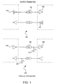
- FIG. 1 is a schematic diagram illustrating both source and parallel termination approaches. Either approach may be employed to implement an embodiment in accordance with the present invention: however, the embodiment described hereinafter is implemented as a source termination circuit to capture cost and speed advantages that may be available with that approach.
- electrical signals such as digital signals in this particular embodiment, are communicated from a source driver, such as 110 or 250, to a destination driver, such as 150 or 260.
- these signals are transmitted via a coupling, such as 140 or 240 having an impedance Z 0 .
- Performance is improved relative to alternative approaches if the well-known technique of impedance matching is employed.
- electrical signals that may be reflected by the destination driver are property terminated. In this context, this means that substantially no electrical signal reflections occur at the source end of the coupling.
- a source termination approach or a parallel termination approach may be employed.
- the impedance of the coupling such as 140
- the impedance of the source driver such as 110.
- the impedance is matched via a coupling of the matching impedance, such as 210, to the impedance of the coupling being matched, such as 240.
- interface circuitry may be employed in association with a signal bus, for example, for operation in either a desktop personal computer or a server configuration, for example.
- impedance matching such as previously described, may be employed.
- cost and speed factors may make use of the parallel termination approach on a board or elsewhere less desirable than the source termination approach. Therefore, in this particular embodiment, for example, the impedance of a driver may be matched to the impedance of an external coupling to a network, for example, to achieve these desirable signal speeds.
- impedance matching may involve matching a given impedance to the impedance associated with a particular point on a non-linear current-voltage (I/V) characteristic curve representing the operation of an MOS transistor.
- I/V current-voltage
- the scope of the invention is not limited to a particular approach, such as restricting the range of operation of an MOS transistor or employing a circuit to at least approximately linearize the operation of an MOS transistor; however, for this particular embodiment, due to ease of implementation, instead.
- the impedance to be matched will be matched to a selected point on the MOS transistor current vs. voltage (I/V) characteristic curve.
- I/V current vs. voltage
- Such an approach permits an inverting complementary metal-oxide semiconductor (CMOS) buffer to be used as an output buffer.
- CMOS complementary metal-oxide semiconductor
- noise sources resuming in transitions to other portions of the I/V curve, such as the saturation region of operation of the transistor will not be properly terminated and, therefore, may contribute to intersymbol interference.
- Approximating the impedance of an external coupling by the impedance of a CMOS output buffer may be done in at number of ways. For example, cascoded devices or series gating may be employed. The circuits may be implemented to allow either digital or analog control. For this particular embodiment, although the invention is not limited in scope in this respect, a digital approach is employed due to the potentially noisy environment for the electronic signals.
- a circuit may be implemented using cascoded devices in series with a primary output amplifier to adjust or control the effective impedance of the overall structure.
- the cascode devices may include multiple, parallel couplings that may be individually enabled.
- the weighting of these devices to adjust the effective impedance of the output buffer may be accomplished in a variety of ways, although the invention is not limited in scope to any particular approach.
- Two frequently employed approaches include binary weighting and linear weighting.
- overall device size may affect the available range of impedances that may be implemented, the resolution of the impedance may be affected by the size of the smallest device, such as illustrated in FIG. 3, for example.
- One advantage of binary weighting is that it permits a larger impedance range for a given resolution in comparison with linear weighting: however, as will be explained in more detail hereinafter, it has disadvantages with respect to "on-the-fly" updating of the impedance.
- an alternative approach may employ using series gating to adjust or control the impedance of the output buffer.
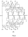
- This particular approach is employed in the embodiment illustrated in FIG. 3. although the invention is not limited in scope to this particular approach.
- the particular approach employed to implement the output buffer may affect additional implementation considerations including the size of the smallest leg, such as due to electrostatic discharge (ESD) sensitivity, and, likewise, the area of the chip employed by the particular buffer. For example, a cascoded approach employs a relatively large area in comparison with a series gated approach.
- the amplifier is a multi-legged device with the input signal being gated with enable signals for the individual legs.
- the term leg refers to the primary transistors employed to implement the amplifier configuration (e.g., 460, 470, 480, 490, 510, 520, 530 and 540).
- the size of the overall amplifier is reduced.
- a speed penalty will be incurred because the predrivers, such as 430 or 440, are more complex, which introduces additional delay.
- the slew rate for the electronic digital signals produced may also be adjusted or controlled. Again, a variety of techniques may be employed, including analog techniques and digital techniques. For the embodiment illustrated in FIG. 3, impedance and slew rate adjustment are both incorporated. In this particular embodiment, a subset of the impedance control couplings are employed to control slew rate. This particular approach reduces the control circuitry and coupling in comparison with an approach in which both impedance control and slew rate control are into the same buffer. In this particular embodiment, a 4-bit control scheme with a 2-bit slew rate control of the 4-bits is employed. Slew rate adjustment may be accomplished, for example, using parallel legs on the predriver for the side of the device that turns on or produces the electrical digital output signal.
- the N-device has multiple legs.
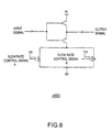
- devices 700 and 710 have been added in cascode with the predriver N-type MOS (NMOS) device.
- Inverters 452 may employ a similar approach using PMOS devices.
- Devices 700 and 710 in FIG.8 are used to control the impedance of the predriver in an approach similar to the approach used to control as the impedance of the output buffer with devices 460, 470, etc.. This impedance driving the capacitance of the output buffers. such as due to devices 460. 470, etc.. limits the slew rate of the output buffer.
- the output buffer turn-on slew rate is controlled in this embodiment because the output buffer is meant to be used in a source-terminated configuration.
- the turn-off slew rate would also be controlled due at least in part to static current in the coupling.
- en3 and en2 are employed for stew rate adjustment.
- An offset value between the nominal values for impedance adjustment and slew rate adjustment may be employed in the control logic, as described in more detail hereinafter. Therefore, if the impedance of the predriver is well-controlled, the slew rate of the driver may be lightly controlled as well.
- a digital control loop may be employed to compensate a digitally controllable buffer, such as previously described. for variations in process and environment, for example.
- a digitally controllable buffer such as previously described. for variations in process and environment, for example.
- Any digitally controllable buffer or even a controllable buffer that is not controllable digitally may be employed.
- noise is present at the signal sampling interface illustrated in FIG. 4, it is desirable to limit the loop bandwidth to reduce the sensitvity to this noise.
- a filter may be implemented in a variety of ways, such as at the sampling pin, in this embodiment, the interface of 330, 340, and 360, or in control logic block 310, to limit the loop bandwidth. Another advantage is that this permits the use of relatively slow circuit components, and permits the lowering of the sampling rate to allow for metastability settling time, as will be described later.
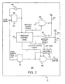
- FIG. 2 is a schematic diagram illustrating an embodiment 300 of an impedance control circuit in accordance with the invention, although the invention is not limited in scope to this particular embodiment.
- Embodiment 300 is illustrated as embodied on an integrated circuit (IC) chip, although the invention is not limited in scope in this respect.
- an externally derived clock signal drives the control circuit: however, it is divided down by divider 442.
- Output buffer 320 comprises an interface circuit output buffer, while output buffer 330 comprises a non-data signal or "dummy" output buffer.
- a feedback control loop including amplifier 360 and impedance control logic 310 is coupled to adjust the impedance of output buffer 330 based, at least in part, on the impedance of external coupling 340.
- the feedback control circuit operates to approximately match the impedance of buffer 330 with, in this particular embodiment, the impedance of external resistor 340.
- resistors 370 and 350 effectively establish the voltage signal reference level for amplifier 360.
- Impedance control logic 310 based, at least in part, on the output signal of amplifier 360 controls whether to adjust the impedance of buffer 330 up or down, that is increase or decrease the buffer impedence.
- this control signal information is also applied to buffer 320.
- the feedback control circuit also produces control signals to adjust the slew rate of buffer 320 based on the impedance control signals produced from operation of the feedback loop including buffer 330.
- register 410 is employed so that buffer 320 may be updated "on-the-fly," as explained in more detail hereinafter.
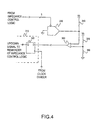
- FIG. 4 illustrates a portion of the embodiment of FIG. 2.
- a precision external resistor 340 is coupled to an output port of non-data signal (dummy) output buffer 330.
- the impedance value obtained for buffer 330 due to the operation of the feedback circuit previously described is then used to adjust the impedance of output buffer 320.
- a reference voltage signal level for amplifier 360 is generated. This reference voltage signal level is implemented in this embodiment by resistors 350 and 370 in FIG. 4. This sets the threshold for amplifier 360.
- This reference value effectively sets the point on the MOS transistor I/V characteristic to which the impedance of buffer 330 is matched.
- Resistor 340 is selected by approximating the nominal value of the external coupling to buffer 320.
- an externally derived coupling may be employed in place of resistor 340 or another approach may be employed.
- the feedback control circuit in this embodiment operates as follows.
- a sample impedance signal value is taken by input latch 305.
- a first predetermined period of time elapses to allow any metastabilities in the latch to settle.
- a determination regarding which direction to adjust the impedance of buffer 330 is made, that is to increase or decrease the impedence.
- This may be implemented in 310, for example, by adjusting the value of an up/down counter or a shift register to control the impedance of buffer 330, as explained later. Therefore, impedance control logic 310 generates signals applied to buffer 330 to produce the next impedance value.
- control circuit 310 results in the impedance of buffer 330 varying by plus or minus a least significant control bit about the desired impedance value.
- the time to allow for metastability settling and for settling of the transition of output buffer 330 is provided in this embodiment by a clock divider, as illustrated in FIG. 4. As illustrated. logic in the control loop is clocked by this divided down clock signal. It is desirable to set the clock or sampling rate to obtain a reasonably low sampling error rate due to metastable states in input latch 305. These metastabilities may occur from noise on the dummy pin at any time with respect to the clock, and may, therefore, violate the setup and hold conditions of latch 305. Computation of the mean time between failures of a latch involves parameters such as the process technology, latch design, allowable settling time, and probability distribution of the latch data edge timing with respect to the clock.
- an acceptable settling time may be calculated. For example, for a latch which samples uniformly distributed asynchronous data signals (and making some simplifying assumptions) at a frequency of approximately 433 Megahertz, it is desirable to divide the clock by at least two generated sampling clock pulses, although the invention is not limited in scope in this respect. Thus for this embodiment, divider 442 provides an acceptable settling time for the target process, although the invention is not limited in scope in this respect.
- FIG. 5 illustrates the filter employed in this embodiment, although, again, the invention is not limited in scope to employing a filter or to this particular embodiment.
- the pole of the filter it is desirable to avoid instabilities. Therefore, it is desirable to update the impedance at a lower rate than the bandwidth of the loop to allow the loop time to settle after an update.
- the pole of the analog filter is placed at less than half the sampling frequency, but at least two times the update rate, although the invention is not limited in this respect. In the time domain response, therefore, after the impedance is updated, the next sampling event occurs after two filter time constants. Of course, a greater number of filter time constants before the next sampling event may be employed, however, doing so would also increase the control loop lock time.
- the control loop should lock with a one-bit variation from the matching point and, therefore, oscillate. It is desirable to remove this oscillation from the actual output signal produced by buffer 320.
- a simple digital notch filter may be employed. For example, a simple, exclusive or circuit may be employed. If successive digital sample values are the same then an update of buffer 320 is performed, however, if successive samples are not the same, then the last update is retained by buffer 320. This particular embodiment is illustrated in FIG. 6. As illustrated, impedance control block 310 provides signals to output buffer 330.
- the output signals of low pass filter 610 are provided to notch filter 620.
- Notch filter 620 provides a signal to block 407.
- the impedance control signals produced by 310 are also provided by block 407 to register 640 and, therefore, to register 410 and ultimately to buffer 320.
- impedance control block 307 is dependent, at (east in part, on the weighting of the output buffer legs.
- a shift register may be employed.
- this block may be implemented as an up/down counter.
- one bit of a shift register would change on each impedance update, changing the impedance of the buffer by a substantially uniform amount.
- a counter is updated, producing another binary digital signal value controlling the buffer impedance. In such an embodiment, therefore, all bits of the counter may change on a single impedance update. As illustrated in FIG.
- adder 650 is used to offset the nominal slew rate value from the nominal impedance value.
- This offset value may be set either internally or externally by a variety of techniques.
- the offset value may be loaded into a register from an external source, or alternatively, it may be implemented with fuses. For example, if it were intended to use the same output buffer to match several alternative impedances, and it were desirable to maintain a substantially constant slew rate. it would he desirable to be able to modify this offset value.
- this embodiment includes the capability to adjust the impedance of the output buffer while the output buffer is transmitting data signals.
- One problem with this "on-the-fly" updating is that if the update occurs temporally near an outgoing data signal edge, for example, it may alter the timing of the edge. This may produce undesirable timing jitter. For example, for the case of a binary weighted output buffer with five legs, a significant change in the impedance of the output buffer may occur in a single clock cycle. With linear encoding. because only one bit at a time changes, the impact of this effect is reduced. However, linear encoding provides a smaller range of impedance values.
- an additional problem may result because after a large change in impedance, some output buffer legs may turn on relatively slowly due to slew rate control. This may occur in this embodiment since, for source terminated buffers, "turn off" of a leg is done quickly, while “turn on” of a leg is done slowly to implement slew rate control.
- the impedance control signal values from 310 may change from 1000 to 0111 on a single impedance update. If the most significant bit changes first, the buffer may tristate momentarily. If non-zero current was in the signal transmission coupling when the buffer tristated, the line will switch. The remaining impedance control bits will then switch, turning the buffer back on and returning the coupling approximately to it's original state, but slowly. The line, therefore, glitches. This may degrade performance if the output buffer is transmitting data signals while this occurs.
- on-the-fly updating is performed by updating while the output buffer is in tri-state or by updating the "off" or non-transmitting side of the CMOS output buffer (for example, in this embodiment, the NMOS devices while the output signal is high, and the PMOS devices while the output signal is low).
- latches are employed at each individual leg of the output buffer using register 410 of FIG. 2, in this embodiment, for example.
- the latches used in register 410 are replicated at each signal output port; however, these latches may be relatively small.
- signals RESET and OEn are employed so that "on-the-fly" updating occurs during tri-state or reset.
- on-the-fly updating is employed only for the impedance of the output buffer.
- the slew rate control may be operated for a few clock cycles after reset to remove process variations, for example, and then the slew rate value may be locked.
- on-the-fly updating of the slew rate may likewise be employed, although this may also create timing jitter.
- An embodiment of a method of adjusting an impedance of an interface circuit output buffer may be accomplished as follows.
- the impedance of a non-data signal output buffer such as output buffer 330 in FIG. 2, coupled to an external impedance, such as resistor 340 in FIG. 2 may be digitally adjusted.
- the impedance of an interface circuit output buffer such as output buffer 320 in FIG. 2, may be digitally adjusted based, at least in part, on digitally adjusted impedance of the non-data signal output buffer.
- the impedance of the interface circuit output buffer may also be digitally adjusted based, at least in part, on the digital adjustment of the impedance of the non-data signal output buffer.
- the impedance of the interface circuit output buffer may be digitally adjusted on-the-fly.
- the impedance of the non-transmitting side of the interface circuit output buffer may be digitally adjusted on-the-fly.
- digitally adjusting the impedance of the non-data signal output buffer comprises approximately matching the impedance of the non-data signal output buffer, such as buffer 330 in FIG. 2, with the impedance of the external coupling, such as resistor 340 in FIG. 2.
- the impedance of the non-data signal output buffer is digitally adjusted so that the external impedance is source terminated.
- digitally adjusting the impedance of a non-data signal output buffer coupled to an external impedance comprises digitally adjusting the impedance in binary weighted increments, although, again, the invention is not limited in scope in this respect.
Description
Claims (15)
- An integrated circuit comprising:a digital feedback control circuit (300) arranged to (a) adjust an interface circuit output buffer (320) impedance based, at least in part, on adjustments to an impedance of a non-data signal output buffer (330) coupled to an external impedance (340), and (b) adjust the slew rate of said interface circuit output buffer (320).
- The integrated circuit of claim 1, wherein said digital feedback control circuit (300) includes the capability to adjust the impedance of said interface circuit output buffer on-the-fly.
- The integrated circuit of claim 2, wherein the capability to adjust the impedance of said interface circuit output buffer on-the-fly comprises the capability to adjust the impedance of the non-transmitting side (450) of said interface circuit output buffer on-the-fly.
- The integrated circuit of claim 2, wherein said digital feedback control circuit to adjust the impedance of said interface circuit output buffer (320) comprises a digital feedback control circuit to approximately match the impedance of said non-data signal output buffer (330) with the impedance of the external impedance (340).
- The integrated circuit of claim 1, wherein said external impedance comprises at least one resistor (340).
- The integrated circuit of claim 1, wherein said digital feedback control circuit comprises a source termination digital feedback control circuit (140 and 110).
- The integrated circuit of claim 1, wherein said interface circuit output buffer (320) comprises an output buffer in which at least some of the transistors are series gated.
- The integrated circuit of claim 1, wherein said interface circuit output buffer includes an amplifier configuration (460, 470, 480, 490, 510, 520, 530, and 540) with a plurality of legs, said legs being sized so that their weighting to adjust the effective impedance of the output buffer is substantially binary.
- A method of adjusting the impedance of an interface circuit output buffer (320) comprising:digitally adjusting the impedance of a non-data signal output buffer (330) coupled to an external impedance (340);digitally adjusting the impedance of the interface circuit output buffer based, at least in part, on the digitally adjusted impedance of the non-data signal output buffer, anddigitally adjusting the slew rate of the interface circuit output buffer.
- The method of claim 9, wherein digitally adjusting the impedance of the interface circuit output buffer includes digitally adjusting the impedance on-the-fly.
- The method of claim 10, wherein digitally adjusting the impedance of the interface circuit output buffer on-the-fly comprises digitally adjusting the impedance of the non-transmitting side (450) of the interface circuit buffer on-the-fly.
- The method of claim 9, wherein adjusting the impedance of the non-data signal output buffer comprises approximately matching the impedance of the non-data signal output buffer with the impedance of the external impedance (340).
- The method of claim 12, wherein the external impedance comprises at least one resistor (340).
- The method of claim 9, wherein digitally adjusting the impedance of a non-data signal output buffer coupled to an external impedance comprises digitally adjusting the impedance of the non-data signal output buffer so that the external impedance is source terminated (110 and 140).
- The method of claim 9, wherein digitally adjusting the impedance of a non-data signal output buffer coupled to an external impedance comprises digitally adjusting the impedance in binary weighted increments (450, 700 and 710).
Applications Claiming Priority (3)
| Application Number | Priority Date | Filing Date | Title |
|---|---|---|---|
| US08/902,345 US6087847A (en) | 1997-07-29 | 1997-07-29 | Impedance control circuit |
| US902345 | 1997-07-29 | ||
| PCT/US1998/014846 WO1999006845A2 (en) | 1997-07-29 | 1998-07-17 | Impedance control circuit |
Publications (3)
| Publication Number | Publication Date |
|---|---|
| EP1010013A2 EP1010013A2 (en) | 2000-06-21 |
| EP1010013A4 EP1010013A4 (en) | 2000-10-18 |
| EP1010013B1 true EP1010013B1 (en) | 2004-03-17 |
Family
ID=25415727
Family Applications (1)
| Application Number | Title | Priority Date | Filing Date |
|---|---|---|---|
| EP98935769A Expired - Lifetime EP1010013B1 (en) | 1997-07-29 | 1998-07-17 | Impedance control circuit |
Country Status (9)
| Country | Link |
|---|---|
| US (1) | US6087847A (en) |
| EP (1) | EP1010013B1 (en) |
| JP (1) | JP4274688B2 (en) |
| KR (1) | KR20010022326A (en) |
| AU (1) | AU8495298A (en) |
| DE (1) | DE69822479T2 (en) |
| HK (1) | HK1027398A1 (en) |
| TW (1) | TW461995B (en) |
| WO (1) | WO1999006845A2 (en) |
Cited By (1)
| Publication number | Priority date | Publication date | Assignee | Title |
|---|---|---|---|---|
| CN102279833A (en) * | 2006-06-02 | 2011-12-14 | 拉姆伯斯公司 | Integrated circuit with graduated on-die termination |
Families Citing this family (90)
| Publication number | Priority date | Publication date | Assignee | Title |
|---|---|---|---|---|
| US6393062B1 (en) * | 1998-09-21 | 2002-05-21 | Maxim Integrated Products, Inc. | Methods and circuits for generating a preemphasis waveform |
| CA2388385A1 (en) * | 1999-05-15 | 2000-11-23 | John W.L. Ogilvie | Automatic broker tools and techniques |
| JP4101973B2 (en) * | 1999-05-21 | 2008-06-18 | 株式会社ルネサステクノロジ | Output buffer circuit |
| US6292407B1 (en) * | 1999-10-12 | 2001-09-18 | Micron Technolgy, Inc. | Method and apparatus for circuit variable updates |
| US6300789B1 (en) * | 1999-12-22 | 2001-10-09 | Intel Corporation | Dynamic termination for non-symmetric transmission line network topologies |
| US6566903B1 (en) * | 1999-12-28 | 2003-05-20 | Intel Corporation | Method and apparatus for dynamically controlling the performance of buffers under different performance conditions |
| US6331785B1 (en) * | 2000-01-26 | 2001-12-18 | Cirrus Logic, Inc. | Polling to determine optimal impedance |
| US6501292B1 (en) * | 2000-03-02 | 2002-12-31 | Intel Corporation | CMOS circuit for maintaining a constant slew rate |
| US6462588B2 (en) * | 2000-04-03 | 2002-10-08 | Rambus, Inc. | Asymmetry control for an output driver |
| US6329836B1 (en) * | 2000-05-26 | 2001-12-11 | Sun Microsystems, Inc. | Resistive arrayed high speed output driver with pre-distortion |
| US6392441B1 (en) * | 2000-06-13 | 2002-05-21 | Ramtron International Corporation | Fast response circuit |
| US6624659B1 (en) * | 2000-06-30 | 2003-09-23 | Intel Corporation | Dynamically updating impedance compensation code for input and output drivers |
| US7222208B1 (en) | 2000-08-23 | 2007-05-22 | Intel Corporation | Simultaneous bidirectional port with synchronization circuit to synchronize the port with another port |
| US6424175B1 (en) | 2000-09-11 | 2002-07-23 | Intel Corporation | Biased control loop circuit for setting impedance of output driver |
| KR100356576B1 (en) * | 2000-09-15 | 2002-10-18 | 삼성전자 주식회사 | programmable data output circuit with programmable on chip termination operation and method therefore |
| US6445245B1 (en) * | 2000-10-06 | 2002-09-03 | Xilinx, Inc. | Digitally controlled impedance for I/O of an integrated circuit device |
| US6445170B1 (en) | 2000-10-24 | 2002-09-03 | Intel Corporation | Current source with internal variable resistance and control loop for reduced process sensitivity |
| KR100391148B1 (en) * | 2000-11-02 | 2003-07-16 | 삼성전자주식회사 | Programmable impedance control circuit and method |
| US6420899B1 (en) | 2000-12-29 | 2002-07-16 | Intel Corporation | Dynamic impedance matched driver for improved slew rate and glitch termination |
| US6396301B1 (en) * | 2001-01-19 | 2002-05-28 | Dell Products L.P. | Ground bounce prediction methodology and use of same in data error reduction |
| US6529041B1 (en) | 2001-03-23 | 2003-03-04 | Xilinx, Inc. | System power control output circuit for programmable logic devices |
| US6448807B1 (en) | 2001-03-29 | 2002-09-10 | Intel Corporation | Dynamic impedance controlled driver for improved slew rate and glitch termination |
| US6448811B1 (en) | 2001-04-02 | 2002-09-10 | Intel Corporation | Integrated circuit current reference |
| US6522174B2 (en) * | 2001-04-16 | 2003-02-18 | Intel Corporation | Differential cascode current mode driver |
| US6507225B2 (en) | 2001-04-16 | 2003-01-14 | Intel Corporation | Current mode driver with variable equalization |
| US6545522B2 (en) * | 2001-05-17 | 2003-04-08 | Intel Corporation | Apparatus and method to provide a single reference component for multiple circuit compensation using digital impedance code shifting |
| US6535047B2 (en) * | 2001-05-17 | 2003-03-18 | Intel Corporation | Apparatus and method to use a single reference component in a master-slave configuration for multiple circuit compensation |
| US6597233B2 (en) | 2001-05-25 | 2003-07-22 | International Business Machines Corporation | Differential SCSI driver rise time and amplitude control circuit |
| US6791356B2 (en) * | 2001-06-28 | 2004-09-14 | Intel Corporation | Bidirectional port with clock channel used for synchronization |
| US6603329B1 (en) | 2001-08-29 | 2003-08-05 | Altera Corporation | Systems and methods for on-chip impedance termination |
| US6798237B1 (en) | 2001-08-29 | 2004-09-28 | Altera Corporation | On-chip impedance matching circuit |
| US6529037B1 (en) | 2001-09-13 | 2003-03-04 | Intel Corporation | Voltage mode bidirectional port with data channel used for synchronization |
| US6525569B1 (en) * | 2001-09-21 | 2003-02-25 | International Business Machines Corporation | Driver circuit having shapable transition waveforms |
| US6590413B1 (en) | 2001-10-03 | 2003-07-08 | Altera Corporation | Self-tracking integrated differential termination resistance |
| US6597198B2 (en) | 2001-10-05 | 2003-07-22 | Intel Corporation | Current mode bidirectional port with data channel used for synchronization |
| US6812732B1 (en) | 2001-12-04 | 2004-11-02 | Altera Corporation | Programmable parallel on-chip parallel termination impedance and impedance matching |
| US6836144B1 (en) | 2001-12-10 | 2004-12-28 | Altera Corporation | Programmable series on-chip termination impedance and impedance matching |
| US6812734B1 (en) | 2001-12-11 | 2004-11-02 | Altera Corporation | Programmable termination with DC voltage level control |
| US7109744B1 (en) | 2001-12-11 | 2006-09-19 | Altera Corporation | Programmable termination with DC voltage level control |
| US6642742B1 (en) * | 2002-03-21 | 2003-11-04 | Advanced Micro Devices, Inc. | Method and apparatus for controlling output impedance |
| JP4212309B2 (en) * | 2002-07-01 | 2009-01-21 | 株式会社ルネサステクノロジ | Semiconductor integrated circuit |
| KR100495660B1 (en) * | 2002-07-05 | 2005-06-16 | 삼성전자주식회사 | Semiconductor integrated circuit having on-die termination circuit |
| US6836142B2 (en) | 2002-07-12 | 2004-12-28 | Xilinx, Inc. | Asymmetric bidirectional bus implemented using an I/O device with a digitally controlled impedance |
| US6963218B1 (en) | 2002-08-09 | 2005-11-08 | Xilinx, Inc. | Bi-directional interface and communication link |
| US7194559B2 (en) * | 2002-08-29 | 2007-03-20 | Intel Corporation | Slave I/O driver calibration using error-nulling master reference |
| US6930506B2 (en) * | 2002-10-22 | 2005-08-16 | International Business Machines Corporation | Terminating resistor driver for high speed data communication |
| US20040212399A1 (en) * | 2002-11-29 | 2004-10-28 | Daniel Mulligan | Programmable driver for use in a multiple function handheld device |
| US6998875B2 (en) * | 2002-12-10 | 2006-02-14 | Ip-First, Llc | Output driver impedance controller |
| US6985008B2 (en) * | 2002-12-13 | 2006-01-10 | Ip-First, Llc | Apparatus and method for precisely controlling termination impedance |
| US6949949B2 (en) * | 2002-12-17 | 2005-09-27 | Ip-First, Llc | Apparatus and method for adjusting the impedance of an output driver |
| US6788100B2 (en) * | 2003-01-31 | 2004-09-07 | Blueheron Semiconductor Corporation | Resistor mirror |
| US7129738B2 (en) * | 2003-03-04 | 2006-10-31 | Micron Technology, Inc. | Method and apparatus for calibrating driver impedance |
| JP4428504B2 (en) * | 2003-04-23 | 2010-03-10 | 株式会社ルネサステクノロジ | Semiconductor integrated circuit device |
| US20040263203A1 (en) * | 2003-06-27 | 2004-12-30 | Intel Corporation | Signal compensation |
| US6888369B1 (en) | 2003-07-17 | 2005-05-03 | Altera Corporation | Programmable on-chip differential termination impedance |
| US6888370B1 (en) | 2003-08-20 | 2005-05-03 | Altera Corporation | Dynamically adjustable termination impedance control techniques |
| US6859064B1 (en) | 2003-08-20 | 2005-02-22 | Altera Corporation | Techniques for reducing leakage current in on-chip impedance termination circuits |
| US7330993B2 (en) * | 2003-09-29 | 2008-02-12 | Intel Corporation | Slew rate control mechanism |
| JP4086757B2 (en) * | 2003-10-23 | 2008-05-14 | Necエレクトロニクス株式会社 | Input / output interface circuit of semiconductor integrated circuit |
| JP4290537B2 (en) * | 2003-11-26 | 2009-07-08 | 株式会社ルネサステクノロジ | Semiconductor device |
| EP1700377A1 (en) * | 2003-12-23 | 2006-09-13 | Koninklijke Philips Electronics N.V. | Load-aware circuit arrangement |
| TWI304529B (en) * | 2004-01-30 | 2008-12-21 | Realtek Semiconductor Corp | Impedance control circuit and method thereof |
| KR100640782B1 (en) * | 2004-04-16 | 2006-11-06 | 주식회사 하이닉스반도체 | A semiconductor memory device |
| US7248636B2 (en) * | 2004-04-20 | 2007-07-24 | Hewlett-Packard Development Company, L.P. | Systems and methods for adjusting an output driver |
| US7126394B2 (en) * | 2004-05-17 | 2006-10-24 | Micron Technology, Inc. | History-based slew rate control to reduce intersymbol interference |
| JP4536449B2 (en) * | 2004-07-29 | 2010-09-01 | 富士通株式会社 | Driver circuit, semiconductor device, and electronic device |
| FR2878665B1 (en) * | 2004-11-30 | 2007-05-25 | St Microelectronics Rousset | TRANSCONDUCTANCE AMPLIFIER CIRCUIT WITH NEGATIVE GAIN |
| US7218155B1 (en) | 2005-01-20 | 2007-05-15 | Altera Corporation | Techniques for controlling on-chip termination resistance using voltage range detection |
| US7221193B1 (en) | 2005-01-20 | 2007-05-22 | Altera Corporation | On-chip termination with calibrated driver strength |
| KR100702838B1 (en) * | 2005-05-09 | 2007-04-03 | 삼성전자주식회사 | Impedance controllable output driving circuit in semiconductor device and impedance control method therefore |
| US7679397B1 (en) | 2005-08-05 | 2010-03-16 | Altera Corporation | Techniques for precision biasing output driver for a calibrated on-chip termination circuit |
| KR100746200B1 (en) | 2005-10-21 | 2007-08-06 | 삼성전자주식회사 | Source driver, Source driver module, and display device |
| US8213894B2 (en) * | 2005-12-29 | 2012-07-03 | Intel Corporation | Integrated circuit passive signal distribution |
| US20070252638A1 (en) * | 2006-04-26 | 2007-11-01 | Farrukh Aquil | Method and apparatus for temperature compensating off chip driver (OCD) circuit |
| KR100733449B1 (en) | 2006-06-30 | 2007-06-28 | 주식회사 하이닉스반도체 | On die termination of semiconductor |
| JP4958719B2 (en) * | 2006-10-20 | 2012-06-20 | ルネサスエレクトロニクス株式会社 | Semiconductor integrated circuit |
| TW200910373A (en) | 2007-06-08 | 2009-03-01 | Mosaid Technologies Inc | Dynamic impedance control for input/output buffers |
| US7550993B2 (en) * | 2007-08-21 | 2009-06-23 | Texas Instruments Incorporated | Glitch reduced compensated circuits and methods for using such |
| US7876123B2 (en) * | 2007-10-09 | 2011-01-25 | Lsi Corporation | High speed multiple memory interface I/O cell |
| JP5059580B2 (en) * | 2007-12-20 | 2012-10-24 | ルネサスエレクトロニクス株式会社 | Termination circuit |
| JP5109647B2 (en) * | 2007-12-25 | 2012-12-26 | 凸版印刷株式会社 | Driver circuit |
| US7969181B1 (en) * | 2008-02-03 | 2011-06-28 | Freescale Semiconductor, Inc. | Device and method for adjusting an impedance of an output driver of an integrated circuit |
| US7653505B1 (en) * | 2008-03-14 | 2010-01-26 | Xilinx, Inc. | Method and apparatus for testing a controlled impedance buffer |
| US7443194B1 (en) * | 2008-04-24 | 2008-10-28 | International Business Machines Corporation | I/O driver for integrated circuit with output impedance control |
| JP5584401B2 (en) * | 2008-08-23 | 2014-09-03 | ピーエスフォー ルクスコ エスエイアールエル | Semiconductor device and data processing system including the same |
| US7821290B2 (en) * | 2008-09-26 | 2010-10-26 | Vitesse Semiconductor Corporation | Differential voltage mode driver and digital impedance caliberation of same |
| US20100164471A1 (en) * | 2008-12-30 | 2010-07-01 | M2000 | Calibration of programmable i/o components using a virtual variable external resistor |
| US7888968B2 (en) * | 2009-01-15 | 2011-02-15 | International Business Machines Corporation | Configurable pre-emphasis driver with selective constant and adjustable output impedance modes |
| US8030968B1 (en) * | 2010-04-07 | 2011-10-04 | Intel Corporation | Staged predriver for high speed differential transmitter |
| JP2014146409A (en) * | 2014-03-12 | 2014-08-14 | Ps4 Luxco S A R L | Semiconductor integrated circuit and testing method thereof |
Family Cites Families (9)
| Publication number | Priority date | Publication date | Assignee | Title |
|---|---|---|---|---|
| US5134311A (en) * | 1990-06-07 | 1992-07-28 | International Business Machines Corporation | Self-adjusting impedance matching driver |
| US5243229A (en) * | 1991-06-28 | 1993-09-07 | At&T Bell Laboratories | Digitally controlled element sizing |
| US5254883A (en) * | 1992-04-22 | 1993-10-19 | Rambus, Inc. | Electrical current source circuitry for a bus |
| FR2709217B1 (en) * | 1993-08-19 | 1995-09-15 | Bull Sa | Method and device for impedance adaptation for a transmitter and / or receiver, integrated circuit and transmission system using them. |
| US5457407A (en) * | 1994-07-06 | 1995-10-10 | Sony Electronics Inc. | Binary weighted reference circuit for a variable impedance output buffer |
| JP3484825B2 (en) * | 1995-06-09 | 2004-01-06 | 株式会社デンソー | Driver circuit |
| US5872471A (en) * | 1995-12-25 | 1999-02-16 | Hitachi, Ltd. | Simultaneous bidirectional transmission circuit |
| US5666078A (en) * | 1996-02-07 | 1997-09-09 | International Business Machines Corporation | Programmable impedance output driver |
| US5726583A (en) * | 1996-07-19 | 1998-03-10 | Kaplinsky; Cecil H. | Programmable dynamic line-termination circuit |
-
1997
- 1997-07-29 US US08/902,345 patent/US6087847A/en not_active Expired - Lifetime
-
1998
- 1998-07-17 AU AU84952/98A patent/AU8495298A/en not_active Abandoned
- 1998-07-17 WO PCT/US1998/014846 patent/WO1999006845A2/en active IP Right Grant
- 1998-07-17 DE DE69822479T patent/DE69822479T2/en not_active Expired - Lifetime
- 1998-07-17 EP EP98935769A patent/EP1010013B1/en not_active Expired - Lifetime
- 1998-07-17 JP JP2000505524A patent/JP4274688B2/en not_active Expired - Fee Related
- 1998-07-17 KR KR1020007000905A patent/KR20010022326A/en active Search and Examination
- 1998-07-20 TW TW087111793A patent/TW461995B/en not_active IP Right Cessation
-
2000
- 2000-10-12 HK HK00106494A patent/HK1027398A1/en not_active IP Right Cessation
Cited By (2)
| Publication number | Priority date | Publication date | Assignee | Title |
|---|---|---|---|---|
| CN102279833A (en) * | 2006-06-02 | 2011-12-14 | 拉姆伯斯公司 | Integrated circuit with graduated on-die termination |
| CN102279833B (en) * | 2006-06-02 | 2016-01-06 | 拉姆伯斯公司 | There is the integrated circuit of graduated on-die termination |
Also Published As
| Publication number | Publication date |
|---|---|
| DE69822479D1 (en) | 2004-04-22 |
| TW461995B (en) | 2001-11-01 |
| EP1010013A2 (en) | 2000-06-21 |
| US6087847A (en) | 2000-07-11 |
| JP4274688B2 (en) | 2009-06-10 |
| HK1027398A1 (en) | 2001-01-12 |
| WO1999006845A3 (en) | 1999-09-10 |
| KR20010022326A (en) | 2001-03-15 |
| WO1999006845A2 (en) | 1999-02-11 |
| EP1010013A4 (en) | 2000-10-18 |
| JP2001512296A (en) | 2001-08-21 |
| DE69822479T2 (en) | 2004-08-19 |
| AU8495298A (en) | 1999-02-22 |
Similar Documents
| Publication | Publication Date | Title |
|---|---|---|
| EP1010013B1 (en) | Impedance control circuit | |
| US5808478A (en) | Digitally controlled output buffer to incrementally match line impedance and maintain slew rate independent of capacitive output loading | |
| US5877634A (en) | CMOS buffer with controlled slew rate | |
| JP4724117B2 (en) | Tx line driver with common mode idle state and selectable slew rate | |
| US8324925B2 (en) | Output buffer circuit and differential output buffer circuit, and transmission method | |
| EP0547349A2 (en) | Programmable integrated circuit output pad | |
| JP2002199030A (en) | Printed circuit board, circuit on integrated circuit and method for terminating transmission line | |
| US6570931B1 (en) | Switched voltage adaptive slew rate control and spectrum shaping transmitter for high speed digital transmission | |
| US6452433B1 (en) | High phase margin low power flip-flop | |
| US7038512B2 (en) | Closed-loop independent DLL-controlled rise/fall time control circuit | |
| US7038513B2 (en) | Closed-loop independent DLL-controlled rise/fall time control circuit | |
| KR100266902B1 (en) | Transmission line termination circuit of receipt and communication devices | |
| JP3864255B2 (en) | Impedance control method and circuit | |
| KR100316037B1 (en) | Output buffer circuit | |
| US7961000B1 (en) | Impedance matching circuit and method | |
| US6980019B2 (en) | Output buffer apparatus capable of adjusting output impedance in synchronization with data signal | |
| US7157931B2 (en) | Termination circuits having pull-down and pull-up circuits and related methods | |
| US6239619B1 (en) | Method and apparatus for dynamic termination logic of data buses | |
| US5852372A (en) | Apparatus and method for signal handling on GTL-type buses | |
| US6373276B1 (en) | CMOS small signal switchable impedence and voltage adjustable terminator with hysteresis receiver network | |
| US7339399B2 (en) | Anti-noise input/output impedance control of semiconductor circuit with reduced circuit size | |
| US6310490B1 (en) | CMOS small signal switchable, impedence and voltage adjustable terminator network and receiver integration | |
| US6356104B1 (en) | CMOS small signal switchable, impedence and voltage adjustable terminator network | |
| US7202723B2 (en) | Adjustable switchpoint receiver | |
| US6741657B1 (en) | Circuit arrangement for transmitting pulses via a transmission path |
Legal Events
| Date | Code | Title | Description |
|---|---|---|---|
| PUAI | Public reference made under article 153(3) epc to a published international application that has entered the european phase |
Free format text: ORIGINAL CODE: 0009012 |
|
| 17P | Request for examination filed |
Effective date: 20000217 |
|
| AK | Designated contracting states |
Kind code of ref document: A2 Designated state(s): DE FR GB |
|
| A4 | Supplementary search report drawn up and despatched |
Effective date: 20000906 |
|
| AK | Designated contracting states |
Kind code of ref document: A4 Designated state(s): DE FR GB |
|
| RIC1 | Information provided on ipc code assigned before grant |
Free format text: 7G 01R 3/00 A, 7H 03K 19/00 B |
|
| 17Q | First examination report despatched |
Effective date: 20020718 |
|
| GRAP | Despatch of communication of intention to grant a patent |
Free format text: ORIGINAL CODE: EPIDOSNIGR1 |
|
| GRAS | Grant fee paid |
Free format text: ORIGINAL CODE: EPIDOSNIGR3 |
|
| GRAA | (expected) grant |
Free format text: ORIGINAL CODE: 0009210 |
|
| AK | Designated contracting states |
Kind code of ref document: B1 Designated state(s): DE FR GB |
|
| REG | Reference to a national code |
Ref country code: GB Ref legal event code: FG4D |
|
| REF | Corresponds to: |
Ref document number: 69822479 Country of ref document: DE Date of ref document: 20040422 Kind code of ref document: P |
|
| REG | Reference to a national code |
Ref country code: HK Ref legal event code: GR Ref document number: 1027398 Country of ref document: HK |
|
| ET | Fr: translation filed | ||
| PLBE | No opposition filed within time limit |
Free format text: ORIGINAL CODE: 0009261 |
|
| STAA | Information on the status of an ep patent application or granted ep patent |
Free format text: STATUS: NO OPPOSITION FILED WITHIN TIME LIMIT |
|
| 26N | No opposition filed |
Effective date: 20041220 |
|
| PGFP | Annual fee paid to national office [announced via postgrant information from national office to epo] |
Ref country code: FR Payment date: 20080729 Year of fee payment: 11 |
|
| REG | Reference to a national code |
Ref country code: FR Ref legal event code: ST Effective date: 20100331 |
|
| PG25 | Lapsed in a contracting state [announced via postgrant information from national office to epo] |
Ref country code: FR Free format text: LAPSE BECAUSE OF NON-PAYMENT OF DUE FEES Effective date: 20090731 |
|
| PGFP | Annual fee paid to national office [announced via postgrant information from national office to epo] |
Ref country code: DE Payment date: 20160712 Year of fee payment: 19 Ref country code: GB Payment date: 20160713 Year of fee payment: 19 |
|
| REG | Reference to a national code |
Ref country code: DE Ref legal event code: R119 Ref document number: 69822479 Country of ref document: DE |
|
| GBPC | Gb: european patent ceased through non-payment of renewal fee |
Effective date: 20170717 |
|
| PG25 | Lapsed in a contracting state [announced via postgrant information from national office to epo] |
Ref country code: GB Free format text: LAPSE BECAUSE OF NON-PAYMENT OF DUE FEES Effective date: 20170717 Ref country code: DE Free format text: LAPSE BECAUSE OF NON-PAYMENT OF DUE FEES Effective date: 20180201 |