EP1017104A2 - Ferroelectric intergrated circuit with protective layer incorporating oxygen and method for fabricating same - Google Patents
Ferroelectric intergrated circuit with protective layer incorporating oxygen and method for fabricating same Download PDFInfo
- Publication number
- EP1017104A2 EP1017104A2 EP99122514A EP99122514A EP1017104A2 EP 1017104 A2 EP1017104 A2 EP 1017104A2 EP 99122514 A EP99122514 A EP 99122514A EP 99122514 A EP99122514 A EP 99122514A EP 1017104 A2 EP1017104 A2 EP 1017104A2
- Authority
- EP
- European Patent Office
- Prior art keywords
- ferroelectric
- layer
- oxygen
- integrated circuit
- protective layer
- Prior art date
- Legal status (The legal status is an assumption and is not a legal conclusion. Google has not performed a legal analysis and makes no representation as to the accuracy of the status listed.)
- Withdrawn
Links
Images

Classifications
-
- H—ELECTRICITY
- H10—SEMICONDUCTOR DEVICES; ELECTRIC SOLID-STATE DEVICES NOT OTHERWISE PROVIDED FOR
- H10B—ELECTRONIC MEMORY DEVICES
- H10B53/00—Ferroelectric RAM [FeRAM] devices comprising ferroelectric memory capacitors
-
- H—ELECTRICITY
- H01—ELECTRIC ELEMENTS
- H01L—SEMICONDUCTOR DEVICES NOT COVERED BY CLASS H10
- H01L27/00—Devices consisting of a plurality of semiconductor or other solid-state components formed in or on a common substrate
- H01L27/02—Devices consisting of a plurality of semiconductor or other solid-state components formed in or on a common substrate including semiconductor components specially adapted for rectifying, oscillating, amplifying or switching and having at least one potential-jump barrier or surface barrier; including integrated passive circuit elements with at least one potential-jump barrier or surface barrier
- H01L27/04—Devices consisting of a plurality of semiconductor or other solid-state components formed in or on a common substrate including semiconductor components specially adapted for rectifying, oscillating, amplifying or switching and having at least one potential-jump barrier or surface barrier; including integrated passive circuit elements with at least one potential-jump barrier or surface barrier the substrate being a semiconductor body
- H01L27/10—Devices consisting of a plurality of semiconductor or other solid-state components formed in or on a common substrate including semiconductor components specially adapted for rectifying, oscillating, amplifying or switching and having at least one potential-jump barrier or surface barrier; including integrated passive circuit elements with at least one potential-jump barrier or surface barrier the substrate being a semiconductor body including a plurality of individual components in a repetitive configuration
- H01L27/105—Devices consisting of a plurality of semiconductor or other solid-state components formed in or on a common substrate including semiconductor components specially adapted for rectifying, oscillating, amplifying or switching and having at least one potential-jump barrier or surface barrier; including integrated passive circuit elements with at least one potential-jump barrier or surface barrier the substrate being a semiconductor body including a plurality of individual components in a repetitive configuration including field-effect components
-
- H—ELECTRICITY
- H01—ELECTRIC ELEMENTS
- H01L—SEMICONDUCTOR DEVICES NOT COVERED BY CLASS H10
- H01L28/00—Passive two-terminal components without a potential-jump or surface barrier for integrated circuits; Details thereof; Multistep manufacturing processes therefor
- H01L28/40—Capacitors
- H01L28/55—Capacitors with a dielectric comprising a perovskite structure material
-
- H—ELECTRICITY
- H10—SEMICONDUCTOR DEVICES; ELECTRIC SOLID-STATE DEVICES NOT OTHERWISE PROVIDED FOR
- H10B—ELECTRONIC MEMORY DEVICES
- H10B53/00—Ferroelectric RAM [FeRAM] devices comprising ferroelectric memory capacitors
- H10B53/30—Ferroelectric RAM [FeRAM] devices comprising ferroelectric memory capacitors characterised by the memory core region
-
- H—ELECTRICITY
- H01—ELECTRIC ELEMENTS
- H01L—SEMICONDUCTOR DEVICES NOT COVERED BY CLASS H10
- H01L28/00—Passive two-terminal components without a potential-jump or surface barrier for integrated circuits; Details thereof; Multistep manufacturing processes therefor
- H01L28/40—Capacitors
- H01L28/55—Capacitors with a dielectric comprising a perovskite structure material
- H01L28/56—Capacitors with a dielectric comprising a perovskite structure material the dielectric comprising two or more layers, e.g. comprising buffer layers, seed layers, gradient layers
-
- H—ELECTRICITY
- H01—ELECTRIC ELEMENTS
- H01L—SEMICONDUCTOR DEVICES NOT COVERED BY CLASS H10
- H01L2924/00—Indexing scheme for arrangements or methods for connecting or disconnecting semiconductor or solid-state bodies as covered by H01L24/00
- H01L2924/0001—Technical content checked by a classifier
- H01L2924/0002—Not covered by any one of groups H01L24/00, H01L24/00 and H01L2224/00
Definitions
- the invention relates to a ferroelectric integrated circuit having low sensitivity to hydrogen exposure and to a method for fabricating such a circuit.
- Ferroelectric compounds possess favorable characteristics for use in nonvolatile integrated circuit memories. See Miller, U.S. Patent No. 5,046,043.
- a ferroelectric device such as a capacitor, is useful as a nonvolatile memory when it possess desired electronic characteristics, such as high residual polarization, good coercive field, high fatigue resistance, and low leakage current.
- Lead-containing ABO 3 -type ferroelectric oxides such as PZT(lead titanate zirconate) and PLZT (lanthanum lead titanate zirconate) have been studied for practical use in integrated circuits. Layered superlattice material oxides have also been studied for use in integrated circuits. See Watanabe, U.S. Patent No. 5,434,102.
- Layered superlattice material compounds exhibit characteristics in ferroelectric memories that are orders of magnitude superior to those of PZT and PLZT compounds. Integrated circuit devices containing ferroelectric elements are currently being manufactured. Nevertheless, the persistent problem of hydrogen degradation during the manufacturing process hinders the economical production in commercial quantities of ferroelectric memories and other IC devices using the layered superlattice material compounds with the desired electronic characteristics.
- a typical ferroelectric memory device in an integrated circuit contains a semiconductor substrate and a metal-oxide semiconductor field-effect transistor (MOSFET) in electrical contact with a ferroelectric device, usually a ferroelectric capacitor.
- a ferroelectric capacitor typically contains a thin film containing ferroelectric metal oxide located between a first, bottom electrode and a second, top electrode, the electrodes typically containing platinum.
- the MOSFET is subjected to conditions causing defects in the silicon substrate.
- the CMOS/MOSFET manufacturing process usually includes high energy steps, such as ion-mill etching and plasma etching. Defects also arise during heat treatment for crystallization of the ferroelectric thin film at relatively high temperatures, often in the range 500°-900°C. As a result, numerous defects are generated in the single crystal structure of the semiconductor silicon substrate, leading to deterioration in the electronic characteristics of the MOSFET.
- the manufacturing process typically includes a hydrogen annealing step, in which defects such as dangling bonds are eliminated by utilizing the reducing property of hydrogen.
- a hydrogen annealing step in which defects such as dangling bonds are eliminated by utilizing the reducing property of hydrogen.
- Various techniques have been developed to effect the hydrogen annealing, such as a forming-gas anneal ("FGA").
- FGA treatments are conducted under ambient conditions in a H 2 -N 2 gas mixture between 350° and 550°C, typically around 400-450°C, for a time period of about 30 minutes.
- CMOS/MOSFET manufacturing process requires other fabrication steps that expose the integrated circuit to hydrogen, often at elevated temperatures, such as hydrogen-rich plasma CVD processes for depositing metals and dielectrics, growth of silicon dioxide from silane or TEOS sources, and etching processes using hydrogen and hydrogen plasma.
- hydrogen-rich plasma CVD processes for depositing metals and dielectrics
- growth of silicon dioxide from silane or TEOS sources and etching processes using hydrogen and hydrogen plasma.
- hydrogen-rich plasma CVD processes for depositing metals and dielectrics
- silicon dioxide from silane or TEOS sources
- etching processes using hydrogen and hydrogen plasma etching processes using hydrogen and hydrogen plasma.
- the hydrogen diffuses principally through the top electrode to the ferroelectric thin film, but also from the side edges of the capacitor, and reduces the oxides contained in the ferroelectric material.
- the absorbed hydrogen also metallizes the surface of the ferroelectric thin film by reducing metal oxides. As a result of these effects, the electronic properties of the capacitor are degraded.
- the remnant polarization of the ferroelectrics is very low and no longer suitable for storing information.
- An increase in leakage currents also results.
- the adhesivity of the ferroelectric thin film to the upper electrode is lowered by the chemical change taking place at the interface.
- the upper electrode is pushed up by the oxygen gas, water, and other products of the oxidation-reduction reactions taking place.
- peeling is likely to take place at the interface between the top electrode and the ferroelectric thin film.
- hydrogen also can reach the lower electrode, leading to internal stresses that cause the capacitor to peel off its substrate.
- ferroelectric compounds comprise metal oxides.
- the products of the reduction reactions cause an increase in the total volume of the ferroelectric element.
- the ferroelectric thin film exerts an upward pressure on the layers above it.
- the prior art also teaches the application of hydrogen barrier layers to inhibit the diffusion of hydrogen into the ferroelectric or dielectric material.
- the barrier layer is typically applied over the ferroelectric element, but it can also be applied below and to the sides of the element.
- hydrogen barrier layers are not completely effective in preventing hydrogen diffusion.
- a protective layer can be a hydrogen barrier layer, a metallized wiring layer, or another layer or structural component of a ferroelectric integrated circuit.
- a ferroelectric integrated circuit according to the invention typically comprises a distinct hydrogen barrier layer containing a small amount of excess oxygen, or a metallized wiring layer containing a small amount of excess oxygen, or both.
- the invention also provides a method for forming a hydrogen barrier layer and a metallized wiring layer containing small amounts of oxygen. The small amount of oxygen in a protective layer according to the invention forms oxides to protect ferroelectric oxide material from hydrogen degradation.
- the oxides present in the protective layer protect ferroelectric oxides by reacting with hydrogen so that it does not diffuse into the ferroelectric material.
- the formation of the oxides in a hydrogen barrier layer directly over a ferroelectric circuit element exerts a compressive stress in a downward direction.
- the reduction of oxides by hydrogen in the ferroelectric material and other hydrogen reactions in the ferroelectric element cause stresses in the upward direction and can result in peeling of the thin films from the substrate.
- the compressive stress exerted by the hydrogen barrier layer in the downward direction as a result of oxide formation balances the upward stress exerted by the underlying ferroelectric thin film.
- the oxides in the hydrogen barrier layer thereby bring the capacitor stack into a stress equilibrium condition below catastrophic failure.
- One aspect of the invention is the presence of small amounts of oxides near the surfaces of the protective layer
- the oxides serve as "getters" of hydrogen.
- the small amount of oxides in the regions of the protective layer near its surfaces does not significantly decrease the electrical conductivity of the layer.
- the protective layer comprises a hydrogen barrier layer directly over a ferroelectric element.
- the hydrogen barrier layer comprises a nitride of titanium or silicon if the hyrdogen barrier layer is electrically conductive.
- Another aspect of the invention is the presence of small amounts of oxides in metallized wiring layers directly over the ferroelectric element.
- the oxides are located in the regions near the surfaces of the metallized wiring layers.
- the metallized wiring layer comprises aluminum.
- Another aspect of the invention is a protective layer containing a small amount of oxygen that covers the lateral side of a ferroelectric element.
- a further aspect of the invention is the formation of a protective layer in such a manner that there is an oxygen gradient in the layers, with no oxygen present in the interior of the layers.
- the concentration of oxygen is about two weight percent near the surfaces of the protective layer.
- the protective layer comprises a hydrogen barrier layer or a metallized wiring layer. If the protective layer comprises polycrystalline material with a plurality of crystal grains, such as a metal or ceramic material, then the small amount of oxygen is just enough to decorate the grain boundaries.
- a further aspect of the invention is exertion of a downward stress by a hydrogen barrier layer containing a small amount of oxygen, caused by the oxides formed therein.
- the downward stress balances the upward stress exerted by the layers in the ferroelectric element as a result of hydrogen reactions.
- a further aspect of the invention is a fabrication method in which small, varying amounts of oxygen are added to the sputtering gas atmosphere during sputter deposition of the protective layers so that oxygen is included in the regions near the surfaces of the layers, but not in the center region of the layers.
- FIGS. 1-3 depicting ferroelectric integrated circuit devices are not meant to be actual plan or cross-sectional views of any particular portion of an actual integrated circuit device.
- the layers will not be as regular and the thicknesses may have different proportions.
- the various layers in actual devices often are curved and possess overlapping edges.
- the figures instead show idealized representations which are employed to depict more clearly and fully the structure and process of the invention than would otherwise be possible.
- the figures represent only one of innumerable variations of ferroelectric devices that could be fabricated using the method of the invention.
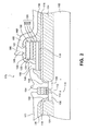
- FIG. 1 there is shown a cross-sectional view of an exemplary nonvolatile ferroelectric memory cell 170 that could be fabricated according to the invention.
- the general manufacturing steps for fabricating integrated circuits containing MOSFETs and ferroelectric capacitor elements are described in Mihara, U.S. Patent No. 5,466,629 and Yoshimori, U.S. Patent No. 5,468,684. General fabrication methods have been described in other references also.
- a field oxide region 104 is formed on a surface of a silicon substrate 102.
- a source region 106 and a drain region 108 are formed separately from each other within silicon substrate 102.
- a gate insulating layer 110 is formed on the silicon substrate 104 between the source and drain regions 106 and 108. Further, a gate electrode 112 is formed on the gate insulating layer 110. These source region 106, drain region 108, gate insulating layer 110, and gate electrode 112 together form a MOSFET 114.
- the adhesion layer 118 is made of, for example, titanium, and typically has a thickness of 20 nm. Adhesion layers, such as titanium, enhance the adhesion of the electrodes to adjacent underlying or overlying layers of the circuits.
- a bottom electrode layer 122 made of platinum and having a thickness of 200 nm is deposited on adhesion layer 118. Then a ferroelectric thin film 124 is formed on bottom electrode layer 122. A top electrode layer 126, made of platinum and having a thickness of 200 nm, is formed on the ferroelectric thin film 124.
- the composition of the ferroelectric thin film 124 is discussed in more detail below.
- a protective layer in this case an electrically-conductive hydrogen barrier layer 130, is deposited on top electrode layer 126.
- Hydrogen barrier layer 130 preferably comprises a nitride of titanium.
- hydrogen barrier layer 130 comprises small amounts of oxygen near its top and bottom surfaces. In FIG. 1, the dots depicted in lower region 131 near the bottom surface of layer 130 represent small amounts of oxygen. Similarly, the dots depicted in upper region 133 near the top surface of layer 130 represent small amounts of oxygen.
- Hydrogen barrier layer 130 preferably comprises crystalline grains.
- the concentration gradient of oxygen in the hydrogen barrier layer 130 is a concentration gradient of oxygen in the hydrogen barrier layer 130, such that the concentration by weight of oxygen in the center region 132 of layer 130 is zero, and the oxygen concentration gradually increases to a value in the range from about one to three weight percent (1-3% wt.) in regions 131, 133 at the bottom and top surfaces of layer 130.
- Region 131 at the bottom of hydrogen barrier layer 130 extends from the bottom surface upward about 10-20% of the total thickness of layer 130.
- region 133 at the top of hydrogen barrier layer 130 extends from the top surface downward about 10-20% of the total thickness of layer 130.
- the oxygen concentration is about two percent (2%) by weight in regions 131, 133.
- the small amounts of oxygen are just enough to decorate the crystalline grain boundaries in the regions 131 and 133. It is believed that TiON located at the grain boundaries increases the activation energy of grain boundary hydrogen diffusion, thereby inhibiting hydrogen diffusion through the layer. The small amounts of oxygen, however, do not substantially decrease the conductivity of the electrically conductive hydrogen barrier layer 130.
- the stack of layers is then patterned in as few as two patterning steps to form a stacked memory capacitor 120 covered by a self-aligned hydrogen barrier l30. For example, as depicted in FIG. 1, portions of layers 124, 126, and 130 are etched away, down to the surface of layer 122. Then, portions of layers 122 and 118 are etched away, down to the surface of layer 116. These patterning steps result in formation of a stacked ferroelectric capacitor 120 covered by self-aligned hydrogen barrier layer 130.
- a second interlayer dielectric layer (ILD) 136 made of NSG (nondoped silicate glass) is deposited to cover ILD 116, ferroelectric capacitor 120, and hydrogen barrier layer 130.
- a PSG (phospho-silicate glass) film or a BPSG (boron phospho-silicate glass) film could also be used in layer 136.
- ILD 136 is patterned to form wiring holes for electrical contacts to MOSFET 114 and ferroelectric capacitor 120.
- Wiring hole 142 is selectively opened through ILD 136 and ILD 116 to expose the source region 106
- wiring hole 144 is selectively opened through ILD 136 and ILD 116 to expose the gate region 108.
- Wiring hole 146 is selectively opened through ILD 136 to expose a portion of the bottom electrode 122.
- Wiring hole 148 is selectively opened through ILD 136 to expose hydrogen barrier layer 130.
- Source electrode wiring 152 and drain electrode wiring 154 are formed to fill wiring holes 142 and 144, respectively.
- Bottom electrode wiring 156 and top electrode wiring 158 are formed to fill the wiring holes 146 and 148, respectively.
- the drain electrode wiring 154 is electrically connected to bottom electrode wiring 156, and preferably is the same wiring element.
- Each of these wirings 152, 154, 156 and 158 preferably comprises Al-Si-Cu standard interconnect metal with a thickness of about 300 nm.
- Fabrication of the ferroelectric element for example, the capacitor in FIG. 1, conventionally involves steps with oxidizing conditions that may damage the switch 114 and other elements of the integrated circuit.
- a hydrogen heat treatment of the circuit is usually performed to repair oxidation damage of the switch.
- the ferroelectric properties of the ferroelectric thin film 124 are prone to degrade because hydrogen can diffuse into ferroelectric thin film 124 and react there with the ferroelectric oxides that the ferroelectric thin film 124 comprises.
- hydrogen diffusion barriers located directly over a ferroelectric element can inhibit hydrogen diffusion arid thereby inhibit hydrogen-degradation of the ferroelectric oxides.
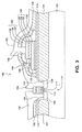
- FIG. 2 is a cross-sectional view of an alternative embodiment of the invention, similar to the embodiment depicted in FIG. 1, but in which a metallized wiring layer 160 of memory cell 175 contains small amounts of oxygen in lower region 161 near its bottom surface, and in upper region 163, near its top surface.
- a concentration gradient of oxygen in the metallized wiring layer 160 such that the concentration by weight of oxygen in the center region 162 of layer 160 is zero, and the oxygen concentration gradually increases to a value in the range from about one to three weight percent (1-3% wt.) in regions 161, 163 near the bottom and top surfaces of layer 160.
- the oxygen concentration is about two percent (2%) by weight in regions 161, 163.
- Region 161 at the bottom of metallized wiring layer 160 extends from the bottom surface upward about 10-20% of the total thickness of layer 160.
- region 163 at the top of metallized wiring layer 160 extends from the top surface downward about 10-20% of the total thickness of layer 160.
- the small amounts of oxygen are just enough to decorate crystalline grain boundaries in regions 161 and 163. It is believed that TiON located at the material grain boundaries increases the activation energy of grain boundary hydrogen diffusion, thereby inhibiting hydrogen diffusion through the layer 160. The small amounts of oxygen, however, do not substantially decrease the conductivity of the metallized wiring layer 160.
- metallized wiring layer 160 comprises aluminum.
- the integrated circuit contains both a hydrogen barrier layer containing oxygen directly over the ferroelectric thin film, and a metallized wiring layer containing oxygen.
- the integrated circuit contains an oxygen-containing metallized wiring layer and no oxygen-containing hydrogen barrier layer, and in another embodiment, it contains an oxygen-containing hydrogen-barrier layer and no oxygen-containing metallized wiring layer.
- at least one structural layer or component of a ferroelectric integrated circuit that is not a metallized wiring layer or hydrogen barrier layer contains a small amount of excess oxygen.
- electrically nonconductive hydrogen barrier layer 135 in ferroelectric memory cell 180 covers the top and sides of stacked capacitor 120.
- bottom electrode layer 122 has a lateral side 123; ferroelectric thin film 124 has a lateral side 125; and top electrode layer 126 has a lateral side 127.
- Lateral sides 123, 125 and 127 together form the sides of stacked capacitor 120.
- the portion of hydrogen barrier layer directly over ferroelectric thin film 124 prevents a significant portion of the hydrogen from diffusing vertically into the ferroelectric thin film through the top electrode layer 126. Yet some of the hydrogen that typically diffuses into a ferroelectric layer diffuses laterally from the edges of the layer.
- hydrogen barrier layer 135 comprises small amounts of oxygen in lower region 137 near its bottom, interior surface, and in upper region 139 near its top, exterior surface. Region 137 at the bottom of hydrogen barrier layer 135 extends from the bottom surface upward about 10-20% of the total thickness of layer 135. Similarly, region 139 at the top of hydrogen barrier layer 135 extends from the top surface downward about 10-20% of the total thickness of layer 135. In FIG. 3, the dots depicted in regions 137 and 139 represent small amounts of oxygen. Hydrogen barrier layer 135 preferably comprises crystalline grains.
- the concentration of oxygen in regions 137, 139 is about two weight percent (2% wt.) at the surfaces.
- wiring holes 146 and 148 must be opened through electrically nonconductive hydrogen barrier layer 135 to make electrical contacts with ferroelectric capacitor 120.
- an electrically nonconductive hydrogen barrier layer covers the sides of capacitor 120, while an electrically conductive hydrogen barrier layer is located directly over ferroelectric thin film 124.
- substrate can mean the underlying wafer 102 on which the integrated circuit is formed, as well as any object on which a thin film layer is deposited, such as BPSG layer 116.
- substrate shall mean the object to which the layer of interest is applied; for example, when we are talking about a bottom electrode, such as 122, the substrate includes the layers 118 and 116 on which the electrode 122 is formed.
- the long dimension of substrate 102 defines a plane that is considered to be a "horizontal” plane herein, and directions perpendicular to this plane are considered to be “vertical”.
- protection layer in this specification refers to a layer or other structural component of a ferroelectric integrated circuit that contains a small amount of oxygen to protect ferroelectric oxide material against hydrogen degradation.
- hydrogen barrier layer means a layer comprising material that is inherently a barrier to hydrogen diffusion, even if the layer contains no excess oxygen. For example, a layer comprising predominantly titanium nitride is a barrier to hydrogen diffusion, even if it contains no oxygen. The presence of small amounts of oxygen, however, enhances the diffusion barrier properties of titanium nitride.
- This specification refers to a protective layer being formed directly over a thin film of ferroelectric material.
- directly over is meant that the protective layer is above at least a portion of the ferroelectric thin film in the vertical direction in FIGS. 1-3.
- the hydrogen barrier layer 130 is directly over ferroelectric thin film 124; it is also directly over bottom electrode layer 122, even though it is not above the portion of bottom electrode 122 in contact with wiring layer 156.
- the term “directly over” does not mean that the protective layer is in direct contact with the ferroelectric layer.
- the protective layer may or may not contact the ferroelectric layer. As long as it is directly over a portion of the ferroelectric layer, it will protect that portion from hydrogen diffusion.
- ferroelectric elements can be fabricated with varying orientations relative to the horizontal and vertical. For example, if the ferroelectric thin film is in the vertical plane, then the word “lateral” would refer to the vertical direction, and “directly over” would refer to an orientation normal to the vertical plane of the thin film.
- the term “on” is often used in the specification when referring to the deposition or formation of an integrated circuit layer onto an underlying substrate or layer. In contrast to “directly over”, the term “on” generally signifies direct contact, as is clear in the various contexts in which it is used.
- small amount and similar terms are used in this specification to refer to oxygen contained in a thin film, layer or other structural component of an integrated circuit.
- "Small amount” means an amount of excess oxygen that does not exceed three weight percent (3% wt.) of the total weight of the designated thin film, layer or structural component.
- the predominant material of the designated structural component typically does not comprise oxides or other oxygen containing compounds; for example, the predominant titanium nitride material in one type of hydrogen barrier layer. But if referring to a ferroelectric oxide layer, then "small amount” would mean an amount of oxygen in excess of the stoichiometrically balanced amount contained in the predominant ferroelectric oxide.
- thin film is used herein as it is used in the integrated circuit art. Generally, it means a film of less than a micron in thickness.
- the thin films disclosed herein are in all instances less than 0.5 microns in thickness.
- the ferroelectric thin films 124 are 100 nm to 300 nm thick, and most preferably 120 nm to 250 nm thick.
- the composition of the ferroelectric thin film 124 can be selected from a group of suitable ferroelectric oxide materials, including but not limited to: an ABO 3 -type perovskite, such as a titanate (e.g., BaTiO 3 , SrTiO 3 , PbTiO 3 (PT), PbZrTiO 3 (PZT)), a niobate (e.g., KNbO 3 ), and, preferably, a layered superlattice compound.
- an ABO 3 -type perovskite such as a titanate (e.g., BaTiO 3 , SrTiO 3 , PbTiO 3 (PT), PbZrTiO 3 (PZT)), a niobate (e.g., KNbO 3 ), and, preferably, a layered superlattice compound.
- a titanate e.g., BaTiO 3 , SrTi
- United States Patent No. 5,519,234, issued May 21, 1996 discloses that layered superlattice compounds, such as strontium bismuth tantalate, have excellent properties in ferroelectric applications as compared to the best prior materials and have high dielectric constants and low leakage currents.
- United States Patents No. 5,434,102, issued July 18, 1995, and No. 5,468,684, issued November 21, 1995 describe processes for integrating these materials into practical integrated circuits.
- the layered superlattice materials may be summarized generally under the formula: A1 +a1 / w1 A2 +a2 / w2 ...Aj +aj / wjS1 +s1 / x1S2 +s2 / x2...Sk +sK / xkB1 +b1 / y1B2 +b2 / y2...BI +bl / ylQ -2 / z, where A1, A2...Aj represent A-site elements in the perovskite-like structure, which may be elements such as strontium, calcium, barium, bismuth, lead, and others; S1,S2...Sk represent superlattice generator elements, which usually is bismuth, but can also be materials such as yttrium, scandium, lanthanum, antimony, chromium, thallium, and other elements with a valence of +3; B1, B2...BI represent B-site elements in the perovskite-
- formula (1) indicates the valences of the respective elements, and the subscripts indicate the number of moles of the material in a mole of the compound; or in terms of the unit cell, the number of atoms of the element, on the average, in the unit cell.
- the subscripts can be integer or fractional. That is, formula (1) includes the cases where the unit cell may vary throughout the material, e.g. in Sr .75 Ba .25 Bi 2 Ta 2 O 9 , on the average, 75% of the A-sites are occupied by strontium atoms and 25% of the A-sites are occupied by barium atoms.
- Formula (1) includes all three of the Smolenskii type compounds discussed in United States Patent No. 5,519,234, issued May 21, 1996.
- the layered superlattice materials do not include every material that can be fit into the formula (1), but only those which spontaneously form themselves into crystalline structures with distinct alternating layers.
- the term “material” may comprise molecules of different composition.
- the layered superlattice material strontium bismuth tantalum niobate comprises interconnected crystal lattices in which two different kinds of atoms, tantalum and niobium, occupy variously the B-site positions of the crystal structure.
- the terms “layered superlattice material”, “layered superlattice compound”, and “layered superlattice material compound” are used virtually interchangeably in this specification and their meaning is clear from the context.
- stoichiometric herein may be applied to both a solid film of a material, such as a layered superlattice material, or to the precursor for forming a material.
- a solid thin film When it is applied to a solid thin film, it refers to a formula which shows the actual relative amounts of each element in a final solid thin film.
- a precursor When applied to a precursor, it indicates the molar proportion of metals in the precursor.
- a "balanced" stoichiometric formula is one in which there is just enough of each element to form a complete crystal structure of the material with all sites of the crystal lattice occupied, though in actual practice there always will be some defects in the crystal at room temperature.
- both SrBi 2 TaNbO 9 and SrBi 2 Ta 1.44 Nb 0.56 O 9 are balanced stoichiometric formulas.
- a precursor for strontium bismuth tantalum niobate in which the molar proportions of strontium, bismuth, tantalum, and niobium are 1, 2.18, 1.44, and 0.56, respectively, is represented herein by the unbalanced "stoichiometric"formula SrBi 2.18 Ta 1.44 Nb 0.56 O 9 , since it contains excess bismuth beyond what is needed to form a complete crystalline material.
- an "excess" amount of a metallic element means an amount greater than required to bond with the other metals present to make the desired material, with all atomic sites occupied and no amount of any metal left over.
- the molar proportion of bismuth in a solid ferroelectric thin film made according to the process of the invention will generally be less than that in the stoichiometric formula for the precursor.
- ferroelectric nonvolatile memories possessing good electronic properties are fabricated by forming a thin film of strontium bismuth tantalate material comprising chemical elements in proportions approximately represented by the stoichiometric formula SrBi 2 Ta 2 O 9 .
- the precursor for making layered superlattice materials currently preferred by those skilled in the art has the stoichiometric formula SrBi 2.18 Ta 1.44 Nb 0.56 O 9 .
- a precursor with this formula will result in a final solid strontium bismuth tantalum niobate thin film with the balanced stoichiometric formula SrBi 2 Ta 1.44 Nb 0.56 O 9 . That is, the final thin film does not contain excess bismuth because the excess bismuth in the precursor is carried away as bismuth oxide gas during the fabrication process.
- This precursor solution contains amounts of chemical precursors corresponding to the stoichiometric ratio SrBi 2.18 Ta 1.44 Nb 0.56 O 9 .
- This stoichiometric formula is referred to herein as the "standard” formula having the "standard” ratio of niobium to tantalum.
- a precursor having the standard stoichiometric formula includes about 9% excess bismuth. That is, the standard stoichiometric formula includes an amount of bismuth above what is required to bond with all the strontium, tantalum and niobium in the precursor to form a layered superlattice compound with all atomic sites in the crystal occupied.
- ferroelectric layer 124 comprises layered superlattice material with excess B-site metal or excess superlattice generator metal; that is, amounts of at least one metal, such as bismuth and niobium, up to about forty mole-percent above or in addition to that shown in the standard formula.
- Such a ferroelectric material is more resistant to degradation by hydrogen than material made with a precursor having the standard formula.
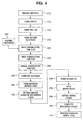
- the diagram of FIG. 4 is a flow sheet of the fabrication steps in accordance with the invention to make a ferroelectric memory 170.
- the ferroelectric memory 170 is preferably formed on a conventional wafer that may be silicon, gallium arsenide or other semiconductor, or an insulator, such as glass or magnesium oxide (MgO).
- Ferroelectric memory 170 preferably comprises a protective layer that is a hydrogen barrier layer.
- a semiconductor substrate 102 (FIG. 1) is provided on which a switch 114 is formed in step 214.
- the switch is typically a MOSFET.
- a first interlayer dielectric layer 116 is formed to separate the switching element from the ferroelectric element to be formed.
- a bottom electrode layer 122 is formed.
- the electrode layer 122 is made of platinum and is sputter-deposited to form a layer with a thickness of about 200 nm.
- an adhesion layer 118 made of titanium or titanium nitride of about 20 nm would be formed in this step, preferably by sputtering, prior to depositing the electrode.
- chemical precursors of the desired ferroelectric thin film are prepared.
- the precursors contain compounds for forming ferroelectric layered superlattice materials.
- the ferroelectric thin film 124 is applied to the bottom electrode layer 122 in step 222.
- the ferroelectric thin film contains layered superlattice compounds.
- a MOCVD method is the most preferred method to form the thin film.
- the ferroelectric thin films also can be applied using a liquid deposition technique, such as a spin-coating or a misted deposition method as described in United States Patent No. 5,456,945.
- a final precursor solution is prepared from commercially available solutions containing the chemical precursor compounds.
- the concentrations of the various precursors supplied in the commercial solutions are adjusted in step 220 to accommodate particular manufacturing or operating conditions.
- the stoichiometric amounts of the various elements in a typical commercial solution for a layered superlattice thin film might be SrBi 2.18 Ta 1.44 Nb 0.56 O 9 .
- the application step 222 is preferably followed by a treatment process 224 which preferably includes a drying step and crystallization substeps at elevated temperatures, such as an oxygen furnace anneal and a rapid thermal process (RTP) anneal; treatment step 224 may include treatment with ultraviolet radiation during or after the application step 222. Steps 222 and 224 may be repeated as necessary to form a film of the desired thickness. For example, in a typical spin-on procedure, a coat of the precursor might be applied and dried. Then another precursor coat might be applied and dried.
- RTP rapid thermal process
- top electrode layer 126 is formed in step 228.
- top electrode layer 126 is made of platinum and is sputter-deposited to form a layer with a thickness of about 200 nm.
- hydrogen barrier layer 130 is deposited.
- hydrogen barrier layer 130 comprises titanium nitride; preferably hydrogen barrier layer 130 is deposited on top electrode layer 126 by a sputtering process.
- the resulting oxides that form in hydrogen barrier layer 130 protect the ferroelectric compounds in the memory device by reacting with the hydrogen that can be present in various manufacturing process steps or by inhibiting hydrogen diffusion.
- step 230 is conducted such that there is a concentration gradient of oxygen in the hydrogen barrier layer 130, so that the concentration by weight of oxygen in the center region 132 of layer 130 is zero, and the oxygen concentration gradually increases to a value in the range from about one to three weight percent (1-3% wt.) in regions 131, 133 at the bottom and top surfaces of layer 130.
- the oxygen concentration is about two percent (2%) by weight in regions 131, 133 near the surfaces.
- Patterning steps via processes such as ion milling and ashing, as known in the art, are also included as appropriate in the fabrication of ferroelectric memory cell 170.
- step 218 may include such a patterning step, and another such patterning step may follow step 226.
- a plurality of layers are patterned in a single patterning step, such as in step 232.
- Barrier layer formation step 230 is preferably followed by a patterning process 232 in which the stacked layers 118, 122, 124, 126 and 130 are patterned to form ferroelectric capacitor 120, covered by self-aligning hydrogen barrier layer 130.
- only two etching processes are required to complete the patterning process of step 232.
- step 232 a conventional ion milling process is utilized in step 232.
- a second ILD layer 136 is then deposited in step 234 to cover ILD 116 and capacitor 120, including hydrogen barrier layer 130.
- wiring holes 142, 144, 146, and 148 are made through the ILD layers 116 and 136, as depicted in FIGS. 1 and 2, to the switch 114 (typically to the source and drain regions of a MOSFET), to the bottom electrode 122, and to hydrogen barrier layer 130, respectively.
- step 236 is performed using a standard ion milling process.
- wiring layers 152, 154, 156, and 158 are deposited, as depicted in FIG. 1, preferably using a sputtering process.
- metallized wiring layer 160 which is directly over ferroelectric layer 120.
- small amounts of oxygen are formed in metallized wiring layer 160 in upper region 161 near its top surface, and in upper region 163, near its bottom surface.
- the concentration gradient of oxygen in the metallized wiring layer 160 is such that the concentration by weight of oxygen in the center region 162 of layer 160 is zero, and the oxygen concentration gradually increases to a value in the range from about one to three weight percent (1-3% wt.) in regions 161, 163 near the bottom and top surfaces of layer 160.
- the oxygen concentration is about two percent (2%) by weight in regions 161, 163.
- small amounts of O 2 -gas are added to the sputter gas atmosphere during formation of regions 161 and 163 of wiring layer 160 to form small amounts of aluminum oxide near the top and bottom surfaces of the layer 160.
- step 240 hydrogen annealing is performed in step 240 to repair defects and restore desired semiconductor properties in the switch (MOSFET) 114.
- the hydrogen anneal of the integrated circuit is conducted at atmospheric pressure in a H 2 -N 2 (forming gas) gas mixture with one to ten percent (1-10%) H 2 , at a temperature of between 200° and 400°C for a time duration of from 10 to 40 minutes.
- the circuit is completed in the step 242, which typically includes deposition of a passivation layer and packaging.
- electrically nonconductive hydrogen barrier layer 135 of ferroelectric memory cell 180 is formed in step 230 to cover the top and sides of stacked capacitor 120.
- small amounts of oxygen are formed in hydrogen barrier layer 135 in lower region 137 near its bottom interior surface, and in upper region 139 near its top, exterior surface.
- the dots depicted in regions 137 and 139 represent small amounts of oxygen.
- a concentration gradient of oxygen is formed in the hydrogen barrier layer 135, such that the concentration by weight of oxygen in the center region 138 of layer 135 is zero, and the oxygen concentration gradually increases to a value in the range of from about one percent to three percent by weight (1-3% wt.) in regions 137, 139 at the surfaces of layer 135.
- the concentration of oxygen in regions 137, 139 is about two weight percent (2% wt.) near the surfaces.
- wiring holes 146 and 148 must be opened through electrically nonconductive hydrogen barrier layer 135 to make electrical contacts with ferroelectric capacitor 120.
- the combination of one or more protective layers, such as oxygen-containing hydrogen barrier layer 130, 135, and excess oxides in ferroelectric thin film 124 is sufficient to protect the ferroelectric thin film 124 from significant degradation upon conventional hydrogen processes.
- one or more protective layers such as oxygen-containing hydrogen barrier layer 130, 135, and excess oxides in ferroelectric thin film 124
- the method of the invention contemplates the use of various other steps to protect the memory device from damage by hydrogen. These steps can be used in conjunction with oxygen-containing protective layers, such as hydrogen barrier layer 130, 135 and oxide-containing metallized wiring layer 160.
- holes for the MOSFET contact wiring can be opened before hydrogen treatment, while holes through the insulating layer to the electrodes of the ferroelectric element can be made after the hydrogen heat treatment step.
- ferroelectric properties can be obtained by using precursors with excess metal, such as excess bismuth and/or excess niobium.
- additional oxygen in integrated circuit layers laid down subsequent to the ferroelectric layers such as an ILD layer laid down subsequent to the fabrication of the ferroelectric layer, which oxygen acts as a "getter” for hydrogen during subsequent hydrogen treatments, can also be effectively used either alone or in combination with one or more of the above measures.
- the invention can be applied to processes and/or structures that enable the prevention of the degradation of ferroelectric elements in combination with almost any exposure to hydrogen that is necessary to create and perfect the other portions of the integrated circuit.
Abstract
Description
- The invention relates to a ferroelectric integrated circuit having low sensitivity to hydrogen exposure and to a method for fabricating such a circuit.
- Ferroelectric compounds possess favorable characteristics for use in nonvolatile integrated circuit memories. See Miller, U.S. Patent No. 5,046,043. A ferroelectric device, such as a capacitor, is useful as a nonvolatile memory when it possess desired electronic characteristics, such as high residual polarization, good coercive field, high fatigue resistance, and low leakage current. Lead-containing ABO3-type ferroelectric oxides such as PZT(lead titanate zirconate) and PLZT (lanthanum lead titanate zirconate) have been studied for practical use in integrated circuits. Layered superlattice material oxides have also been studied for use in integrated circuits. See Watanabe, U.S. Patent No. 5,434,102. Layered superlattice material compounds exhibit characteristics in ferroelectric memories that are orders of magnitude superior to those of PZT and PLZT compounds. Integrated circuit devices containing ferroelectric elements are currently being manufactured. Nevertheless, the persistent problem of hydrogen degradation during the manufacturing process hinders the economical production in commercial quantities of ferroelectric memories and other IC devices using the layered superlattice material compounds with the desired electronic characteristics.
- A typical ferroelectric memory device in an integrated circuit contains a semiconductor substrate and a metal-oxide semiconductor field-effect transistor (MOSFET) in electrical contact with a ferroelectric device, usually a ferroelectric capacitor. A ferroelectric capacitor typically contains a thin film containing ferroelectric metal oxide located between a first, bottom electrode and a second, top electrode, the electrodes typically containing platinum. During manufacture of the circuit, the MOSFET is subjected to conditions causing defects in the silicon substrate. For example, the CMOS/MOSFET manufacturing process usually includes high energy steps, such as ion-mill etching and plasma etching. Defects also arise during heat treatment for crystallization of the ferroelectric thin film at relatively high temperatures, often in the range 500°-900°C. As a result, numerous defects are generated in the single crystal structure of the semiconductor silicon substrate, leading to deterioration in the electronic characteristics of the MOSFET.
- To restore the silicon properties of the MOSFET/CMOS, the manufacturing process typically includes a hydrogen annealing step, in which defects such as dangling bonds are eliminated by utilizing the reducing property of hydrogen. Various techniques have been developed to effect the hydrogen annealing, such as a forming-gas anneal ("FGA"). Conventionally, FGA treatments are conducted under ambient conditions in a H2-N2 gas mixture between 350° and 550°C, typically around 400-450°C, for a time period of about 30 minutes. In addition, the CMOS/MOSFET manufacturing process requires other fabrication steps that expose the integrated circuit to hydrogen, often at elevated temperatures, such as hydrogen-rich plasma CVD processes for depositing metals and dielectrics, growth of silicon dioxide from silane or TEOS sources, and etching processes using hydrogen and hydrogen plasma. During processes that involve hydrogen, the hydrogen diffuses principally through the top electrode to the ferroelectric thin film, but also from the side edges of the capacitor, and reduces the oxides contained in the ferroelectric material. The absorbed hydrogen also metallizes the surface of the ferroelectric thin film by reducing metal oxides. As a result of these effects, the electronic properties of the capacitor are degraded. After the forming-gas anneal (FGA), the remnant polarization of the ferroelectrics is very low and no longer suitable for storing information. An increase in leakage currents also results. In addition, the adhesivity of the ferroelectric thin film to the upper electrode is lowered by the chemical change taking place at the interface. Alternatively, the upper electrode is pushed up by the oxygen gas, water, and other products of the oxidation-reduction reactions taking place. Thus, peeling is likely to take place at the interface between the top electrode and the ferroelectric thin film. In addition, hydrogen also can reach the lower electrode, leading to internal stresses that cause the capacitor to peel off its substrate. These problems are acute in ferroelectric memories containing layered superlattice material compounds because these oxide compounds are particularly complex and prone to degradation by hydrogen-reduction.
- A related problem encountered in the fabrication of ferroelectric devices is the stress arising in and between the different circuit layers as a result of the manufacturing processes. The ferroelectric compounds comprise metal oxides. The products of the reduction reactions cause an increase in the total volume of the ferroelectric element. As a result, the ferroelectric thin film exerts an upward pressure on the layers above it.
- Several methods have been reported in the art to inhibit or reverse hydrogen degradation of desired electronic properties in ferroelectric oxide materials. Oxygen-recovery annealing at high temperature (800°C) for about one hour results in virtually complete recovery of the ferroelectric properties degraded by hydrogen treatments. But the high-temperature oxygen-anneal itself might generate defects in silicon crystalline structure, thereby offsetting somewhat the positive effects of any prior forming-gas anneal on the CMOS characteristics. Also, a high-temperature oxygen-anneal may only be conducted prior to aluminum metallization. Furthermore, if hydrogen treatments have caused structural damage to the ferroelectric device, such as peeling, then a recovery anneal is not able to reverse effectively the damage.
- To reduce the detrimental effects of the hydrogen heat treatment and protect the ferroelectric metal oxide element, the prior art also teaches the application of hydrogen barrier layers to inhibit the diffusion of hydrogen into the ferroelectric or dielectric material. The barrier layer is typically applied over the ferroelectric element, but it can also be applied below and to the sides of the element. Typically, hydrogen barrier layers are not completely effective in preventing hydrogen diffusion. Thus, even when a hydrogen diffusion barrier is used, it is not uncommon for structural damage to arise in the ferroelectric device and for hydrogen to reach the ferroelectric layer and degrade the ferroelectric properties of the ferroelectric material.
- Therefore, it would be useful to have an integrated circuit with a ferroelectric memory device and a method for making such a circuit that would enhance the benefits of various measures used to protect ferroelectric oxide material, in particular, ferroelectric layered superlattice materials, from hydrogen degradation, while minimizing the complexity of the integrated circuit and its fabrication method.
- The invention solves the above problems by providing an integrated circuit in which at least one protective layer of a ferroelectric integrated circuit contains a small amount of oxygen. A protective layer can be a hydrogen barrier layer, a metallized wiring layer, or another layer or structural component of a ferroelectric integrated circuit. A ferroelectric integrated circuit according to the invention typically comprises a distinct hydrogen barrier layer containing a small amount of excess oxygen, or a metallized wiring layer containing a small amount of excess oxygen, or both. The invention also provides a method for forming a hydrogen barrier layer and a metallized wiring layer containing small amounts of oxygen. The small amount of oxygen in a protective layer according to the invention forms oxides to protect ferroelectric oxide material from hydrogen degradation. The oxides present in the protective layer protect ferroelectric oxides by reacting with hydrogen so that it does not diffuse into the ferroelectric material. In addition, the formation of the oxides in a hydrogen barrier layer directly over a ferroelectric circuit element exerts a compressive stress in a downward direction. The reduction of oxides by hydrogen in the ferroelectric material and other hydrogen reactions in the ferroelectric element cause stresses in the upward direction and can result in peeling of the thin films from the substrate. The compressive stress exerted by the hydrogen barrier layer in the downward direction as a result of oxide formation balances the upward stress exerted by the underlying ferroelectric thin film. The oxides in the hydrogen barrier layer thereby bring the capacitor stack into a stress equilibrium condition below catastrophic failure.
- One aspect of the invention is the presence of small amounts of oxides near the surfaces of the protective layer The oxides serve as "getters" of hydrogen. The small amount of oxides in the regions of the protective layer near its surfaces does not significantly decrease the electrical conductivity of the layer.
- Preferably, the protective layer comprises a hydrogen barrier layer directly over a ferroelectric element. Preferably, the hydrogen barrier layer comprises a nitride of titanium or silicon if the hyrdogen barrier layer is electrically conductive.
- Another aspect of the invention is the presence of small amounts of oxides in metallized wiring layers directly over the ferroelectric element. The oxides are located in the regions near the surfaces of the metallized wiring layers.
- Preferably, the metallized wiring layer comprises aluminum.
- Another aspect of the invention is a protective layer containing a small amount of oxygen that covers the lateral side of a ferroelectric element.
- A further aspect of the invention is the formation of a protective layer in such a manner that there is an oxygen gradient in the layers, with no oxygen present in the interior of the layers. Preferably, the concentration of oxygen is about two weight percent near the surfaces of the protective layer. Typically, the protective layer comprises a hydrogen barrier layer or a metallized wiring layer. If the protective layer comprises polycrystalline material with a plurality of crystal grains, such as a metal or ceramic material, then the small amount of oxygen is just enough to decorate the grain boundaries.
- A further aspect of the invention is exertion of a downward stress by a hydrogen barrier layer containing a small amount of oxygen, caused by the oxides formed therein. The downward stress balances the upward stress exerted by the layers in the ferroelectric element as a result of hydrogen reactions.
- A further aspect of the invention is a fabrication method in which small, varying amounts of oxygen are added to the sputtering gas atmosphere during sputter deposition of the protective layers so that oxygen is included in the regions near the surfaces of the layers, but not in the center region of the layers.
- Numerous other features, objects and advantages of the invention will become apparent from the following description when read in conjunction with the accompanying drawings.
-
- FIG. 1 is a cross-sectional view of an integrated circuit in accordance with the invention in which a stacked nonvolatile capacitor is capped by an electrically conductive hydrogen barrier layer containing small amounts of oxygen near its top and bottom surfaces;
- FIG. 2 is a cross-sectional view of an alternative embodiment of the invention, similar to the embodiment depicted in FIG. 1, but in which a metallized wiring layer contains small amounts of oxygen near its top and bottom surfaces;
- FIG. 3 is a cross-sectional view of an integrated circuit in accordance with an alternative embodiment of the invention in which the top and sides of a ferroelectric capacitor are covered by an electrically nonconductive hydrogen barrier layer containing small amounts of oxygen near its top and bottom surfaces;
- FIG. 4 is a flow chart showing a preferred embodiment of a process for fabricating a nonvolatile ferroelectric memory device according to the invention.
-
- It should be understood that the FIGS. 1-3 depicting ferroelectric integrated circuit devices are not meant to be actual plan or cross-sectional views of any particular portion of an actual integrated circuit device. In the actual devices, the layers will not be as regular and the thicknesses may have different proportions. The various layers in actual devices often are curved and possess overlapping edges. The figures instead show idealized representations which are employed to depict more clearly and fully the structure and process of the invention than would otherwise be possible. Also, the figures represent only one of innumerable variations of ferroelectric devices that could be fabricated using the method of the invention. FIGS. 1-3 depict a ferroelectric memory containing a switch in the form of a field effect transistor in electrical connection with a ferroelectric capacitor. But it would also be conceivable to use the method of this invention to fabricate a ferroelectric FET memory in which the ferroelectric element is incorporated in the switch element. Such a ferroelectric FET was described in McMillan, U.S. Patent No. 5,523,964. Likewise, other integrated circuits fabricated using the method of the invention could include other elements and compositions of material.
- In FIG. 1, there is shown a cross-sectional view of an exemplary nonvolatile
ferroelectric memory cell 170 that could be fabricated according to the invention. The general manufacturing steps for fabricating integrated circuits containing MOSFETs and ferroelectric capacitor elements are described in Mihara, U.S. Patent No. 5,466,629 and Yoshimori, U.S. Patent No. 5,468,684. General fabrication methods have been described in other references also. - In FIG. 1, a
field oxide region 104 is formed on a surface of asilicon substrate 102. Asource region 106 and adrain region 108 are formed separately from each other withinsilicon substrate 102. Agate insulating layer 110 is formed on thesilicon substrate 104 between the source and drainregions gate electrode 112 is formed on thegate insulating layer 110. Thesesource region 106,drain region 108,gate insulating layer 110, andgate electrode 112 together form aMOSFET 114. - A first interlayer dielectric layer (ILD) 116 made of BPSG (boron-doped phosphosilicate glass) is formed on
substrate 104 andfield oxide region 102. Anadhesion layer 118 is formed onILD 116. Theadhesion layer 118 is made of, for example, titanium, and typically has a thickness of 20 nm. Adhesion layers, such as titanium, enhance the adhesion of the electrodes to adjacent underlying or overlying layers of the circuits. - As depicted in FIG. 1, a
bottom electrode layer 122 made of platinum and having a thickness of 200 nm is deposited onadhesion layer 118. Then a ferroelectricthin film 124 is formed onbottom electrode layer 122. Atop electrode layer 126, made of platinum and having a thickness of 200 nm, is formed on the ferroelectricthin film 124. The composition of the ferroelectricthin film 124 is discussed in more detail below. - A protective layer, in this case an electrically-conductive
hydrogen barrier layer 130, is deposited ontop electrode layer 126.Hydrogen barrier layer 130 preferably comprises a nitride of titanium. In accordance with the invention,hydrogen barrier layer 130 comprises small amounts of oxygen near its top and bottom surfaces. In FIG. 1, the dots depicted inlower region 131 near the bottom surface oflayer 130 represent small amounts of oxygen. Similarly, the dots depicted inupper region 133 near the top surface oflayer 130 represent small amounts of oxygen.Hydrogen barrier layer 130 preferably comprises crystalline grains. Preferably, there is a concentration gradient of oxygen in thehydrogen barrier layer 130, such that the concentration by weight of oxygen in thecenter region 132 oflayer 130 is zero, and the oxygen concentration gradually increases to a value in the range from about one to three weight percent (1-3% wt.) inregions layer 130.Region 131 at the bottom ofhydrogen barrier layer 130 extends from the bottom surface upward about 10-20% of the total thickness oflayer 130. Similarly,region 133 at the top ofhydrogen barrier layer 130 extends from the top surface downward about 10-20% of the total thickness oflayer 130. Preferably, the oxygen concentration is about two percent (2%) by weight inregions regions hydrogen barrier layer 130. - The stack of layers is then patterned in as few as two patterning steps to form a
stacked memory capacitor 120 covered by a self-aligned hydrogen barrier l30. For example, as depicted in FIG. 1, portions oflayers layer 122. Then, portions oflayers layer 116. These patterning steps result in formation of a stackedferroelectric capacitor 120 covered by self-alignedhydrogen barrier layer 130. - A second interlayer dielectric layer (ILD) 136 made of NSG (nondoped silicate glass) is deposited to cover
ILD 116,ferroelectric capacitor 120, andhydrogen barrier layer 130. A PSG (phospho-silicate glass) film or a BPSG (boron phospho-silicate glass) film could also be used inlayer 136. -
ILD 136 is patterned to form wiring holes for electrical contacts to MOSFET 114 andferroelectric capacitor 120.Wiring hole 142 is selectively opened throughILD 136 andILD 116 to expose thesource region 106, andwiring hole 144 is selectively opened throughILD 136 andILD 116 to expose thegate region 108.Wiring hole 146 is selectively opened throughILD 136 to expose a portion of thebottom electrode 122.Wiring hole 148 is selectively opened throughILD 136 to exposehydrogen barrier layer 130. -
Source electrode wiring 152 anddrain electrode wiring 154 are formed to fillwiring holes Bottom electrode wiring 156 andtop electrode wiring 158 are formed to fill the wiring holes 146 and 148, respectively. Thedrain electrode wiring 154 is electrically connected tobottom electrode wiring 156, and preferably is the same wiring element. Each of thesewirings - Fabrication of the ferroelectric element, for example, the capacitor in FIG. 1, conventionally involves steps with oxidizing conditions that may damage the
switch 114 and other elements of the integrated circuit. After the ferroelectric element has been formed, a hydrogen heat treatment of the circuit is usually performed to repair oxidation damage of the switch. During this hydrogen treatment, as well as during other high-energy steps, the ferroelectric properties of the ferroelectricthin film 124 are prone to degrade because hydrogen can diffuse into ferroelectricthin film 124 and react there with the ferroelectric oxides that the ferroelectricthin film 124 comprises. Generally, hydrogen diffusion barriers located directly over a ferroelectric element can inhibit hydrogen diffusion arid thereby inhibit hydrogen-degradation of the ferroelectric oxides. Nevertheless, typical hydrogen diffusion barriers are not able to completely prevent hydrogen degradation of the ferroelectric oxides. The presence of small amounts of oxygen inhydrogen barrier layer 130 enhances the ability ofhydrogen barrier layer 130 to inhibit hydrogen diffusion, and thereby enhances protection of the ferroelectricthin film 124. - FIG. 2 is a cross-sectional view of an alternative embodiment of the invention, similar to the embodiment depicted in FIG. 1, but in which a metallized
wiring layer 160 ofmemory cell 175 contains small amounts of oxygen inlower region 161 near its bottom surface, and inupper region 163, near its top surface. Preferably, there is a concentration gradient of oxygen in the metallizedwiring layer 160, such that the concentration by weight of oxygen in thecenter region 162 oflayer 160 is zero, and the oxygen concentration gradually increases to a value in the range from about one to three weight percent (1-3% wt.) inregions layer 160. Preferably, the oxygen concentration is about two percent (2%) by weight inregions Region 161 at the bottom of metallizedwiring layer 160 extends from the bottom surface upward about 10-20% of the total thickness oflayer 160. Similarly,region 163 at the top of metallizedwiring layer 160 extends from the top surface downward about 10-20% of the total thickness oflayer 160. The small amounts of oxygen are just enough to decorate crystalline grain boundaries inregions layer 160. The small amounts of oxygen, however, do not substantially decrease the conductivity of the metallizedwiring layer 160. Preferably, metallizedwiring layer 160 comprises aluminum. Preferably, the integrated circuit contains both a hydrogen barrier layer containing oxygen directly over the ferroelectric thin film, and a metallized wiring layer containing oxygen. But in one embodiment of the invention, the integrated circuit contains an oxygen-containing metallized wiring layer and no oxygen-containing hydrogen barrier layer, and in another embodiment, it contains an oxygen-containing hydrogen-barrier layer and no oxygen-containing metallized wiring layer. In still another embodiment, at least one structural layer or component of a ferroelectric integrated circuit that is not a metallized wiring layer or hydrogen barrier layer contains a small amount of excess oxygen. - In an alternative preferred embodiment, as shown in FIG. 3, electrically nonconductive
hydrogen barrier layer 135 inferroelectric memory cell 180 covers the top and sides ofstacked capacitor 120. As depicted in FIG. 3,bottom electrode layer 122 has alateral side 123; ferroelectricthin film 124 has alateral side 125; andtop electrode layer 126 has alateral side 127.Lateral sides stacked capacitor 120. The portion of hydrogen barrier layer directly over ferroelectricthin film 124 prevents a significant portion of the hydrogen from diffusing vertically into the ferroelectric thin film through thetop electrode layer 126. Yet some of the hydrogen that typically diffuses into a ferroelectric layer diffuses laterally from the edges of the layer. The portion ofhydrogen barrier layer 135 coveringlateral sides capacitor 120 towards ferroelectricthin film 124. In accordance with the invention,hydrogen barrier layer 135 comprises small amounts of oxygen inlower region 137 near its bottom, interior surface, and inupper region 139 near its top, exterior surface.Region 137 at the bottom ofhydrogen barrier layer 135 extends from the bottom surface upward about 10-20% of the total thickness oflayer 135. Similarly,region 139 at the top ofhydrogen barrier layer 135 extends from the top surface downward about 10-20% of the total thickness oflayer 135. In FIG. 3, the dots depicted inregions Hydrogen barrier layer 135 preferably comprises crystalline grains. Preferably, there is a concentration gradient of oxygen in thehydrogen barrier layer 135, such that the concentration by weight of oxygen in thecenter region 138 oflayer 135 is zero, and the oxygen concentration gradually increases to a value in the range of from about one percent to three percent by weight (1-3% wt.) inregions layer 135. Preferably, the concentration of oxygen inregions hydrogen barrier layer 135 to make electrical contacts withferroelectric capacitor 120. In another embodiment of the invention (not shown in the figures), an electrically nonconductive hydrogen barrier layer covers the sides ofcapacitor 120, while an electrically conductive hydrogen barrier layer is located directly over ferroelectricthin film 124. - The word "substrate" can mean the
underlying wafer 102 on which the integrated circuit is formed, as well as any object on which a thin film layer is deposited, such asBPSG layer 116. In this disclosure, "substrate" shall mean the object to which the layer of interest is applied; for example, when we are talking about a bottom electrode, such as 122, the substrate includes thelayers electrode 122 is formed. - The terms "above", "top" and "upper", and "below", "bottom" and "lower" herein, mean relative to the
silicon substrate 102. That is, if a second element is "above" a first element, it means it is farther from thesubstrate 102; and if it is "below" another element, then it is closer to thesubstrate 102 than the other element. The long dimension ofsubstrate 102 defines a plane that is considered to be a "horizontal" plane herein, and directions perpendicular to this plane are considered to be "vertical". - The term "protective layer" in this specification refers to a layer or other structural component of a ferroelectric integrated circuit that contains a small amount of oxygen to protect ferroelectric oxide material against hydrogen degradation. The term "protective layer" includes a hydrogen barrier layer containing small amounts of excess oxygen and a metallized wiring layer containing small amounts of excess oxygen. The term "hydrogen barrier layer" means a layer comprising material that is inherently a barrier to hydrogen diffusion, even if the layer contains no excess oxygen. For example, a layer comprising predominantly titanium nitride is a barrier to hydrogen diffusion, even if it contains no oxygen. The presence of small amounts of oxygen, however, enhances the diffusion barrier properties of titanium nitride.
- This specification refers to a protective layer being formed directly over a thin film of ferroelectric material. By "directly over" is meant that the protective layer is above at least a portion of the ferroelectric thin film in the vertical direction in FIGS. 1-3. For example, in FIG. 1, the
hydrogen barrier layer 130 is directly over ferroelectricthin film 124; it is also directly overbottom electrode layer 122, even though it is not above the portion ofbottom electrode 122 in contact withwiring layer 156. The term "directly over" does not mean that the protective layer is in direct contact with the ferroelectric layer. The protective layer may or may not contact the ferroelectric layer. As long as it is directly over a portion of the ferroelectric layer, it will protect that portion from hydrogen diffusion. It is clear that ferroelectric elements can be fabricated with varying orientations relative to the horizontal and vertical. For example, if the ferroelectric thin film is in the vertical plane, then the word "lateral" would refer to the vertical direction, and "directly over" would refer to an orientation normal to the vertical plane of the thin film. The term "on" is often used in the specification when referring to the deposition or formation of an integrated circuit layer onto an underlying substrate or layer. In contrast to "directly over", the term "on" generally signifies direct contact, as is clear in the various contexts in which it is used. - The term "small amount" and similar terms are used in this specification to refer to oxygen contained in a thin film, layer or other structural component of an integrated circuit. "Small amount" means an amount of excess oxygen that does not exceed three weight percent (3% wt.) of the total weight of the designated thin film, layer or structural component. In this invention, the predominant material of the designated structural component typically does not comprise oxides or other oxygen containing compounds; for example, the predominant titanium nitride material in one type of hydrogen barrier layer. But if referring to a ferroelectric oxide layer, then "small amount" would mean an amount of oxygen in excess of the stoichiometrically balanced amount contained in the predominant ferroelectric oxide.
- The term "thin film" is used herein as it is used in the integrated circuit art. Generally, it means a film of less than a micron in thickness. The thin films disclosed herein are in all instances less than 0.5 microns in thickness. Preferably, the ferroelectric
thin films 124 are 100 nm to 300 nm thick, and most preferably 120 nm to 250 nm thick. These thin films of the integrated circuit art should not be confused with the layered capacitors of the macroscopic capacitor art which are formed by a wholly different process which is incompatible with the integrated circuit art. - The composition of the ferroelectric
thin film 124 can be selected from a group of suitable ferroelectric oxide materials, including but not limited to: an ABO3-type perovskite, such as a titanate (e.g., BaTiO3, SrTiO3, PbTiO3 (PT), PbZrTiO3 (PZT)), a niobate (e.g., KNbO3), and, preferably, a layered superlattice compound. - United States Patent No. 5,519,234, issued May 21, 1996, discloses that layered superlattice compounds, such as strontium bismuth tantalate, have excellent properties in ferroelectric applications as compared to the best prior materials and have high dielectric constants and low leakage currents. United States Patents No. 5,434,102, issued July 18, 1995, and No. 5,468,684, issued November 21, 1995, describe processes for integrating these materials into practical integrated circuits.
- The layered superlattice materials may be summarized generally under the formula:
- The word "compound" used precisely refers to a homogeneous substance in which the identical molecules all comprise the same chemical elements and structure. The term "material" may comprise molecules of different composition. For example, the layered superlattice material strontium bismuth tantalum niobate comprises interconnected crystal lattices in which two different kinds of atoms, tantalum and niobium, occupy variously the B-site positions of the crystal structure. Nevertheless, the terms "layered superlattice material", "layered superlattice compound", and "layered superlattice material compound" are used virtually interchangeably in this specification and their meaning is clear from the context.
- The term "stoichiometric" herein may be applied to both a solid film of a material, such as a layered superlattice material, or to the precursor for forming a material. When it is applied to a solid thin film, it refers to a formula which shows the actual relative amounts of each element in a final solid thin film. When applied to a precursor, it indicates the molar proportion of metals in the precursor. A "balanced" stoichiometric formula is one in which there is just enough of each element to form a complete crystal structure of the material with all sites of the crystal lattice occupied, though in actual practice there always will be some defects in the crystal at room temperature. For example, both SrBi2TaNbO9 and SrBi2Ta1.44Nb0.56O9 are balanced stoichiometric formulas. In contrast, a precursor for strontium bismuth tantalum niobate in which the molar proportions of strontium, bismuth, tantalum, and niobium are 1, 2.18, 1.44, and 0.56, respectively, is represented herein by the unbalanced "stoichiometric"formula SrBi2.18Ta1.44 Nb0.56O9, since it contains excess bismuth beyond what is needed to form a complete crystalline material. In this disclosure, an "excess" amount of a metallic element means an amount greater than required to bond with the other metals present to make the desired material, with all atomic sites occupied and no amount of any metal left over. However, as known in the art, because bismuth oxide is highly volatile and significant heat is used in fabricating electronic devices according to the invention, the molar proportion of bismuth in a solid ferroelectric thin film made according to the process of the invention will generally be less than that in the stoichiometric formula for the precursor. However, the molar proportions of strontium, tantalum, and niobium in ferroelectric thin film made according to the process of the invention will be very close or identical to the molar proportions given in the stoichiometric formula for the precursor. See United States Patent No. 5,434,102 issued to Watanabe, et al.
- It is known in the art that ferroelectric nonvolatile memories possessing good electronic properties are fabricated by forming a thin film of strontium bismuth tantalate material comprising chemical elements in proportions approximately represented by the stoichiometric formula SrBi2Ta2O9. Based on the Watanabe, et al., 5,434,102 patent and related work, the precursor for making layered superlattice materials currently preferred by those skilled in the art has the stoichiometric formula SrBi2.18Ta1.44Nb0.56O9. It is believed that a precursor with this formula will result in a final solid strontium bismuth tantalum niobate thin film with the balanced stoichiometric formula SrBi2Ta1.44Nb0.56O9. That is, the final thin film does not contain excess bismuth because the excess bismuth in the precursor is carried away as bismuth oxide gas during the fabrication process. This precursor solution contains amounts of chemical precursors corresponding to the stoichiometric ratio SrBi2.18Ta1.44Nb0.56O9. This stoichiometric formula is referred to herein as the "standard" formula having the "standard" ratio of niobium to tantalum. A precursor having the standard stoichiometric formula includes about 9% excess bismuth. That is, the standard stoichiometric formula includes an amount of bismuth above what is required to bond with all the strontium, tantalum and niobium in the precursor to form a layered superlattice compound with all atomic sites in the crystal occupied. Preferably,
ferroelectric layer 124 comprises layered superlattice material with excess B-site metal or excess superlattice generator metal; that is, amounts of at least one metal, such as bismuth and niobium, up to about forty mole-percent above or in addition to that shown in the standard formula. Such a ferroelectric material is more resistant to degradation by hydrogen than material made with a precursor having the standard formula. - The diagram of FIG. 4 is a flow sheet of the fabrication steps in accordance with the invention to make a
ferroelectric memory 170. Theferroelectric memory 170 is preferably formed on a conventional wafer that may be silicon, gallium arsenide or other semiconductor, or an insulator, such as glass or magnesium oxide (MgO).Ferroelectric memory 170 preferably comprises a protective layer that is a hydrogen barrier layer. Instep 212, a semiconductor substrate 102 (FIG. 1) is provided on which aswitch 114 is formed instep 214. The switch is typically a MOSFET. Instep 216, a firstinterlayer dielectric layer 116 is formed to separate the switching element from the ferroelectric element to be formed. Instep 218, abottom electrode layer 122 is formed. Preferably, theelectrode layer 122 is made of platinum and is sputter-deposited to form a layer with a thickness of about 200 nm. In the preferred method, anadhesion layer 118 made of titanium or titanium nitride of about 20 nm would be formed in this step, preferably by sputtering, prior to depositing the electrode. Instep 220, chemical precursors of the desired ferroelectric thin film are prepared. Preferably, the precursors contain compounds for forming ferroelectric layered superlattice materials. The ferroelectricthin film 124 is applied to thebottom electrode layer 122 instep 222. In the preferred method, the ferroelectric thin film contains layered superlattice compounds. A MOCVD method is the most preferred method to form the thin film. The ferroelectric thin films also can be applied using a liquid deposition technique, such as a spin-coating or a misted deposition method as described in United States Patent No. 5,456,945. Usually, a final precursor solution is prepared from commercially available solutions containing the chemical precursor compounds. Preferably, the concentrations of the various precursors supplied in the commercial solutions are adjusted instep 220 to accommodate particular manufacturing or operating conditions. For example, the stoichiometric amounts of the various elements in a typical commercial solution for a layered superlattice thin film might be SrBi2.18Ta1.44Nb0.56O9. It is often desirable, however, to add extra niobium or bismuth to this solution to generate extra oxides that will protect the ferroelectric compounds from hydrogen degradation during reducing conditions. Theapplication step 222 is preferably followed by atreatment process 224 which preferably includes a drying step and crystallization substeps at elevated temperatures, such as an oxygen furnace anneal and a rapid thermal process (RTP) anneal;treatment step 224 may include treatment with ultraviolet radiation during or after theapplication step 222.Steps thin film 124 instep 226. Following steps 222-226, thetop electrode layer 126 is formed instep 228. Preferably,top electrode layer 126 is made of platinum and is sputter-deposited to form a layer with a thickness of about 200 nm. Instep 230,hydrogen barrier layer 130 is deposited. Preferably,hydrogen barrier layer 130 comprises titanium nitride; preferablyhydrogen barrier layer 130 is deposited ontop electrode layer 126 by a sputtering process. It is a feature of the invention to include a small amount of O2-gas (between zero and about ten volume percent) in the sputter atmosphere during the initial and latter time periods of the sputter-deposition ofhydrogen barrier layer 130 in whichregions hydrogen barrier layer 130 protect the ferroelectric compounds in the memory device by reacting with the hydrogen that can be present in various manufacturing process steps or by inhibiting hydrogen diffusion. Preferably,step 230 is conducted such that there is a concentration gradient of oxygen in thehydrogen barrier layer 130, so that the concentration by weight of oxygen in thecenter region 132 oflayer 130 is zero, and the oxygen concentration gradually increases to a value in the range from about one to three weight percent (1-3% wt.) inregions layer 130. Preferably, the oxygen concentration is about two percent (2%) by weight inregions - Patterning steps via processes such as ion milling and ashing, as known in the art, are also included as appropriate in the fabrication of
ferroelectric memory cell 170. For example, step 218 may include such a patterning step, and another such patterning step may followstep 226. Preferably, however, a plurality of layers are patterned in a single patterning step, such as instep 232. Barrierlayer formation step 230 is preferably followed by apatterning process 232 in which thestacked layers ferroelectric capacitor 120, covered by self-aligninghydrogen barrier layer 130. Preferably, only two etching processes are required to complete the patterning process ofstep 232. Preferably, a conventional ion milling process is utilized instep 232. Asecond ILD layer 136 is then deposited instep 234 to coverILD 116 andcapacitor 120, includinghydrogen barrier layer 130. Instep 236, wiring holes 142, 144, 146, and 148 are made through the ILD layers 116 and 136, as depicted in FIGS. 1 and 2, to the switch 114 (typically to the source and drain regions of a MOSFET), to thebottom electrode 122, and tohydrogen barrier layer 130, respectively. Preferably,step 236 is performed using a standard ion milling process. Instep 238, wiring layers 152, 154, 156, and 158 are deposited, as depicted in FIG. 1, preferably using a sputtering process. However, CVD processes can also be used, despite their accompanying reducing conditions, becausehydrogen barrier layer 130 protects the ferroelectric oxides ofthin film 124. In a preferred alternative embodiment of the inventive method, small amounts of oxygen are included in metallizedwiring layer 160, which is directly overferroelectric layer 120. Preferably, small amounts of oxygen are formed in metallizedwiring layer 160 inupper region 161 near its top surface, and inupper region 163, near its bottom surface. Preferably, there is a concentration gradient of oxygen in the metallizedwiring layer 160, such that the concentration by weight of oxygen in thecenter region 162 oflayer 160 is zero, and the oxygen concentration gradually increases to a value in the range from about one to three weight percent (1-3% wt.) inregions layer 160. Preferably, the oxygen concentration is about two percent (2%) by weight inregions regions wiring layer 160 to form small amounts of aluminum oxide near the top and bottom surfaces of thelayer 160. - Finally, hydrogen annealing is performed in
step 240 to repair defects and restore desired semiconductor properties in the switch (MOSFET) 114. Preferably, the hydrogen anneal of the integrated circuit is conducted at atmospheric pressure in a H2-N2 (forming gas) gas mixture with one to ten percent (1-10%) H2, at a temperature of between 200° and 400°C for a time duration of from 10 to 40 minutes. The circuit is completed in thestep 242, which typically includes deposition of a passivation layer and packaging. - In an alternative preferred embodiment, as shown in FIG. 3, electrically nonconductive
hydrogen barrier layer 135 offerroelectric memory cell 180 is formed instep 230 to cover the top and sides ofstacked capacitor 120. In accordance with the invention, small amounts of oxygen are formed inhydrogen barrier layer 135 inlower region 137 near its bottom interior surface, and inupper region 139 near its top, exterior surface. In FIG. 3, the dots depicted inregions hydrogen barrier layer 135, such that the concentration by weight of oxygen in thecenter region 138 oflayer 135 is zero, and the oxygen concentration gradually increases to a value in the range of from about one percent to three percent by weight (1-3% wt.) inregions layer 135. Preferably, the concentration of oxygen inregions hydrogen barrier layer 135 to make electrical contacts withferroelectric capacitor 120. - Experiments have shown that lateral diffusion of the hydrogen through the ferroelectric thin film, that is, diffusion in a direction parallel to the plane of the ferroelectric thin film, is slow compared with diffusion in a direction normal to the plane of the ferroelectric film. It is, therefore, believed that extra oxides in the ferroelectric material at the lateral edges of the
ferroelectric layer 124 act as a "getter" for any hydrogen that may penetrate in the lateral direction and protects the rest of the material from hydrogen. Ferroelectricthin film 124 preferably is formed to comprise excess oxides that "get" hydrogen which could otherwise cause hydrogen degradation in the remaining portions of the ferroelectric that are covered by a hydrogen barrier layer. Generally, the combination of one or more protective layers, such as oxygen-containinghydrogen barrier layer thin film 124 is sufficient to protect the ferroelectricthin film 124 from significant degradation upon conventional hydrogen processes. However, depending on the intensity of the hydrogen exposure in the various hydrogenating and reducing steps in a fabrication process, use of additional protective measures can be helpful. For these reasons, the method of the invention contemplates the use of various other steps to protect the memory device from damage by hydrogen. These steps can be used in conjunction with oxygen-containing protective layers, such ashydrogen barrier layer metallized wiring layer 160. - Other process sequences and steps may also be used. For example, holes for the MOSFET contact wiring can be opened before hydrogen treatment, while holes through the insulating layer to the electrodes of the ferroelectric element can be made after the hydrogen heat treatment step.
- To keep the exposure to hydrogen small, a low-temperature, short-duration hydrogen heat treatment should be applied where possible. Also, good ferroelectric properties can be obtained by using precursors with excess metal, such as excess bismuth and/or excess niobium. Further, use of additional oxygen in integrated circuit layers laid down subsequent to the ferroelectric layers, such as an ILD layer laid down subsequent to the fabrication of the ferroelectric layer, which oxygen acts as a "getter" for hydrogen during subsequent hydrogen treatments, can also be effectively used either alone or in combination with one or more of the above measures. In this manner, the invention can be applied to processes and/or structures that enable the prevention of the degradation of ferroelectric elements in combination with almost any exposure to hydrogen that is necessary to create and perfect the other portions of the integrated circuit.
- There has been described a method and structure for fabricating ferroelectric integrated circuits that permit exposure to hydrogen and still result in ferroelectric devices with good electrical properties. It should be understood that the particular embodiments shown in the drawings and described within this specification are for purposes of example and should not be construed to limit the invention which will be described in the claims below. Further, it is evident that those skilled in the art may now make numerous uses and modifications of the specific embodiments described, without departing from the inventive concepts. It is also evident that the steps recited may, in some instances, be performed in a different order; or equivalent structures and processes may be substituted for the various structures and processes described. Consequently, the invention is to be construed as embracing each and every novel feature and novel combination of features present in and/or possessed by the fabrication processes, electronic devices, and electronic device manufacturing methods described.
Claims (14)
- A ferroelectric integrated circuit comprising an integrated circuit portion (170, 175, 180) including a thin film of ferroelectric oxide material (124) and a protective layer (130, 160, 135), characterized in that said protective layer comprises a small amount of oxygen.
- A ferroelectric integrated circuit as in claim 1, further characterized in that said thin film of ferroelectric oxide material (124) has a lateral side (125), and said protective layer (135) covers said lateral side (125).
- A ferroelectric integrated circuit as in claim 1 or 2, further characterized in that said protective layer (130, 135) is a hydrogen barrier layer.
- A ferroelectric integrated circuit as in claim 3, further characterized in that said hydrogen barrier layer comprises a nitride of titanium.
- A ferroelectric integrated circuit as in claim 3, further characterized in that said hydrogen barrier layer comprises a nitride of silicon.
- A ferroelectric integrated circuit as in claim 1 or 2, further characterized in that said thin film of ferroelectric oxide material (124) comprises ferroelectric layered superlattice material.
- A ferroelectric integrated circuit as in claim 6, further characterized in that said ferroelectric layered superlattice material (124) comprises a material selected from the group consisting of strontium bismuth tantalum niobate and strontium bismuth tantalate.
- A ferroelectric integrated circuit as in claim 1, further characterized in that said protective layer (160) comprises a metallized wiring layer.
- A ferroelectric integrated circuit as in claim 8, further characterized in that said metallized wiring layer (160) comprises aluminum.
- A ferroelectric integrated circuit as in claim 1, further characterized in that said integrated circuit portion further includes: a substrate (102, 104, 116, 118); a bottom electrode layer(122) on said substrate, said thin film of ferroelectric oxide material (124) disposed on said bottom electrode; and a top electrode layer (126) disposed on said ferroelectric material, said protective layer (130, 135, 160) disposed above said top electrode layer (126).
- A ferroelectric integrated circuit as in claim 10, further characterized in that said bottom electrode layer (122) has a lateral side (123), said thin film of ferroelectric oxide material (124) has a lateral side (125), and said top electrode layer (126) has a lateral side (127), and said protective layer (135) covers said lateral sides (123, 125, 127).
- A ferroelectric integrated circuit as in claim 1, 2, 10 or 11, further characterized in that said protective layer (130, 135) comprises a lower region (131, 137), a center region (132, 138) and an upper region (133, 139), and further characterized in that said oxygen forms an oxygen concentration gradient in said protective layer (130, 135), such that said center region (132, 138) has an oxygen concentration of zero, and said lower region (131, 137) has an oxygen concentration in a range from one to three weight percent, and said upper region (133, 139) has an oxygen concentration in a range from one to three weight percent.
- A method for fabricating a ferroelectric integrated circuit comprising the steps of:forming an integrated circuit portion including a thin film of ferroelectric oxide material;forming a protective layer; andincluding a small amount of oxygen in said protective layer.
- A method as in claim 24, wherein said protective layer comprises a lower region, a center region and an upper region, and wherein said oxygen forms an oxygen concentration gradient in said protective layer, such that said center region has an oxygen concentration of zero, and said lower region has an oxygen concentration in a range from one to three weight percent, and said upper region has an oxygen concentration in a range from one to three weight percent.
Applications Claiming Priority (2)
| Application Number | Priority Date | Filing Date | Title |
|---|---|---|---|
| US204033 | 1994-03-01 | ||
| US09/204,033 US6225656B1 (en) | 1998-12-01 | 1998-12-01 | Ferroelectric integrated circuit with protective layer incorporating oxygen and method for fabricating same |
Publications (2)
| Publication Number | Publication Date |
|---|---|
| EP1017104A2 true EP1017104A2 (en) | 2000-07-05 |
| EP1017104A3 EP1017104A3 (en) | 2001-08-08 |
Family
ID=22756341
Family Applications (1)
| Application Number | Title | Priority Date | Filing Date |
|---|---|---|---|
| EP99122514A Withdrawn EP1017104A3 (en) | 1998-12-01 | 1999-11-11 | Ferroelectric intergrated circuit with protective layer incorporating oxygen and method for fabricating same |
Country Status (5)
| Country | Link |
|---|---|
| US (1) | US6225656B1 (en) |
| EP (1) | EP1017104A3 (en) |
| JP (1) | JP3970477B2 (en) |
| KR (1) | KR100351025B1 (en) |
| CN (1) | CN1158707C (en) |
Cited By (2)
| Publication number | Priority date | Publication date | Assignee | Title |
|---|---|---|---|---|
| EP1381077A2 (en) * | 2002-07-08 | 2004-01-14 | Matsushita Electric Industrial Co., Ltd. | Capacitor and method for fabricating the same |
| EP1271624A3 (en) * | 2001-06-25 | 2007-09-05 | Matsushita Electric Industrial Co., Ltd. | Capacitor, semiconductor memory device, and method for manufacturing the same |
Families Citing this family (49)
| Publication number | Priority date | Publication date | Assignee | Title |
|---|---|---|---|---|
| JPH10237078A (en) * | 1996-10-14 | 1998-09-08 | Dainippon Printing Co Ltd | Metal complex solution, photosensitive metal complex solution and formation of metal oxide film |
| US20030178658A1 (en) * | 1999-07-13 | 2003-09-25 | Hiroki Shinkawata | Semiconductor memory and method of manufacture thereof |
| US6720096B1 (en) | 1999-11-17 | 2004-04-13 | Sanyo Electric Co., Ltd. | Dielectric element |
| US6492222B1 (en) * | 1999-12-22 | 2002-12-10 | Texas Instruments Incorporated | Method of dry etching PZT capacitor stack to form high-density ferroelectric memory devices |
| US6548343B1 (en) * | 1999-12-22 | 2003-04-15 | Agilent Technologies Texas Instruments Incorporated | Method of fabricating a ferroelectric memory cell |
| US6534809B2 (en) * | 1999-12-22 | 2003-03-18 | Agilent Technologies, Inc. | Hardmask designs for dry etching FeRAM capacitor stacks |
| DE10065976A1 (en) * | 2000-02-25 | 2002-02-21 | Infineon Technologies Ag | Method of manufacturing a semiconductor device |
| DE10066082B4 (en) * | 2000-06-14 | 2006-05-18 | Infineon Technologies Ag | Targeted local production of openings in one layer |
| US6597028B2 (en) * | 2000-06-26 | 2003-07-22 | Ramtron International Corporation | Capacitively coupled ferroelectric random access memory cell and a method for manufacturing the same |
| KR20020004539A (en) * | 2000-07-06 | 2002-01-16 | 박종섭 | Method for forming FeRAM capable of preventing hydrogen diffusion |
| IT1318279B1 (en) * | 2000-07-28 | 2003-07-28 | Getters Spa | CAPACITIVE DEVICE INTEGRATED WITH DIELECTRIC LAYER DEGRADABLE FROM HYDROGEN PROTECTED BY GETTER LAYER. |
| DE10041685C2 (en) * | 2000-08-24 | 2002-06-27 | Infineon Technologies Ag | Process for the production of a microelectronic component |
| JP2004519864A (en) * | 2000-08-24 | 2004-07-02 | コバ・テクノロジーズ・インコーポレイテッド | Single-transistor rare-earth manganite ferroelectric nonvolatile memory cell |
| JP2002151657A (en) * | 2000-11-08 | 2002-05-24 | Sanyo Electric Co Ltd | Dielectric element and manufacturing method therefor |
| JP2002231903A (en) | 2001-02-06 | 2002-08-16 | Sanyo Electric Co Ltd | Dielectric element and method of manufacturing the same |
| WO2002071477A1 (en) | 2001-03-02 | 2002-09-12 | Cova Technologies Incorporated | Single transistor rare earth manganite ferroelectric nonvolatile memory cell |
| KR100410716B1 (en) | 2001-03-07 | 2003-12-18 | 주식회사 하이닉스반도체 | FeRAM capable of connecting bottom electrode to storage node and method for forming the same |
| KR100420117B1 (en) * | 2001-03-12 | 2004-03-02 | 삼성전자주식회사 | Semiconductor device having hydrogen diffusion barrier layer and method of fabricating the same |
| JP2002359358A (en) * | 2001-03-26 | 2002-12-13 | Seiko Epson Corp | Ferroelectric substance storage device and electronic apparatus |
| JP4058971B2 (en) * | 2001-03-26 | 2008-03-12 | セイコーエプソン株式会社 | Ferroelectric memory and electronic equipment |
| US7075134B2 (en) * | 2001-11-29 | 2006-07-11 | Symetrix Corporation | Ferroelectric and high dielectric constant integrated circuit capacitors with three-dimensional orientation for high-density memories, and method of making the same |
| JP4090766B2 (en) * | 2002-03-19 | 2008-05-28 | 富士通株式会社 | Manufacturing method of semiconductor device |
| US6936301B2 (en) * | 2002-05-06 | 2005-08-30 | North Carolina State University | Methods of controlling oxygen partial pressure during annealing of a perovskite dielectric layer |
| US6825517B2 (en) | 2002-08-28 | 2004-11-30 | Cova Technologies, Inc. | Ferroelectric transistor with enhanced data retention |
| US6888736B2 (en) | 2002-09-19 | 2005-05-03 | Cova Technologies, Inc. | Ferroelectric transistor for storing two data bits |
| US6714435B1 (en) | 2002-09-19 | 2004-03-30 | Cova Technologies, Inc. | Ferroelectric transistor for storing two data bits |
| US6876021B2 (en) * | 2002-11-25 | 2005-04-05 | Texas Instruments Incorporated | Use of amorphous aluminum oxide on a capacitor sidewall for use as a hydrogen barrier |
| US6841396B2 (en) | 2003-05-19 | 2005-01-11 | Texas Instruments Incorporated | VIA0 etch process for FRAM integration |
| US6984857B2 (en) * | 2003-07-16 | 2006-01-10 | Texas Instruments Incorporated | Hydrogen barrier for protecting ferroelectric capacitors in a semiconductor device and methods for fabricating the same |
| TWI312536B (en) * | 2003-07-23 | 2009-07-21 | Nanya Technology Corporatio | Method for fabricating semiconductor device having stack-gate structure |
| US7019352B2 (en) * | 2003-08-07 | 2006-03-28 | Texas Instruments Incorporated | Low silicon-hydrogen sin layer to inhibit hydrogen related degradation in semiconductor devices having ferroelectric components |
| US7001821B2 (en) * | 2003-11-10 | 2006-02-21 | Texas Instruments Incorporated | Method of forming and using a hardmask for forming ferroelectric capacitors in a semiconductor device |
| US20050276743A1 (en) * | 2004-01-13 | 2005-12-15 | Jeff Lacombe | Method for fabrication of porous metal templates and growth of carbon nanotubes and utilization thereof |
| US6982448B2 (en) * | 2004-03-18 | 2006-01-03 | Texas Instruments Incorporated | Ferroelectric capacitor hydrogen barriers and methods for fabricating the same |
| CN100463182C (en) * | 2004-10-19 | 2009-02-18 | 精工爱普生株式会社 | Ferroelectric memory and method of manufacturing the same |
| JP4497312B2 (en) * | 2004-10-19 | 2010-07-07 | セイコーエプソン株式会社 | Ferroelectric memory manufacturing method |
| US7180141B2 (en) * | 2004-12-03 | 2007-02-20 | Texas Instruments Incorporated | Ferroelectric capacitor with parallel resistance for ferroelectric memory |
| KR100809685B1 (en) * | 2005-09-13 | 2008-03-06 | 삼성전자주식회사 | Dielectric film, Method of manufacturing the dielectric film and method of manufacturing capacitor using the same |
| JP4997757B2 (en) * | 2005-12-20 | 2012-08-08 | 富士通株式会社 | Thin film capacitor and method for manufacturing the same, electronic device and circuit board |
| US20070190670A1 (en) * | 2006-02-10 | 2007-08-16 | Forest Carl A | Method of making ferroelectric and dielectric layered superlattice materials and memories utilizing same |
| JP2008066615A (en) * | 2006-09-11 | 2008-03-21 | Oki Electric Ind Co Ltd | Semiconductor device, and manufacturing method therefor |
| JP5412754B2 (en) * | 2008-06-18 | 2014-02-12 | 富士通セミコンダクター株式会社 | Semiconductor device and manufacturing method of semiconductor device |
| FR2941297B1 (en) * | 2009-01-19 | 2011-02-11 | Commissariat Energie Atomique | METHOD FOR MANUFACTURING A BOLOMETRIC DETECTOR |
| US9269785B2 (en) | 2014-01-27 | 2016-02-23 | Globalfoundries Inc. | Semiconductor device with ferroelectric hafnium oxide and method for forming semiconductor device |
| JP6489942B2 (en) * | 2015-05-29 | 2019-03-27 | 東芝メモリ株式会社 | Manufacturing method of semiconductor device |
| JP6576235B2 (en) * | 2015-12-21 | 2019-09-18 | 東京エレクトロン株式会社 | Lower electrode of DRAM capacitor and manufacturing method thereof |
| US10930751B2 (en) * | 2017-12-15 | 2021-02-23 | Micron Technology, Inc. | Ferroelectric assemblies |
| EP3581904B1 (en) * | 2018-06-15 | 2021-06-02 | Melexis Technologies NV | Platinum metallisation |
| CN110702743B (en) * | 2019-10-16 | 2021-09-28 | 南京大学 | Nano electromechanical hydrogen sensor and preparation method thereof |
Citations (3)
| Publication number | Priority date | Publication date | Assignee | Title |
|---|---|---|---|---|
| US5481490A (en) * | 1993-10-12 | 1996-01-02 | Olympus Optical Co., Ltd. | Ferroelectric memory |
| US5523595A (en) * | 1990-08-21 | 1996-06-04 | Ramtron International Corporation | Semiconductor device having a transistor, a ferroelectric capacitor and a hydrogen barrier film |
| US5923970A (en) * | 1997-11-20 | 1999-07-13 | Advanced Technology Materials, Inc. | Method of fabricating a ferrolelectric capacitor with a graded barrier layer structure |
Family Cites Families (10)
| Publication number | Priority date | Publication date | Assignee | Title |
|---|---|---|---|---|
| US5046043A (en) * | 1987-10-08 | 1991-09-03 | National Semiconductor Corporation | Ferroelectric capacitor and memory cell including barrier and isolation layers |
| US5434102A (en) | 1991-02-25 | 1995-07-18 | Symetrix Corporation | Process for fabricating layered superlattice materials and making electronic devices including same |
| DE69213094T2 (en) * | 1991-05-08 | 1997-03-06 | Philips Electronics Nv | Method for producing a semiconductor arrangement with a capacitor with a ferroelectric dielectric and semiconductor arrangement with such a capacitor |
| US5508226A (en) | 1991-12-13 | 1996-04-16 | Symetrix Corporation | Low temperature process for fabricating layered superlattice materialsand making electronic devices including same |
| JPH0793969A (en) * | 1993-09-22 | 1995-04-07 | Olympus Optical Co Ltd | Ferroelectric capacitance element |
| US5330931A (en) * | 1993-09-22 | 1994-07-19 | Northern Telecom Limited | Method of making a capacitor for an integrated circuit |
| JP2875733B2 (en) | 1994-02-15 | 1999-03-31 | 松下電子工業株式会社 | Method for manufacturing semiconductor device |
| US5716875A (en) | 1996-03-01 | 1998-02-10 | Motorola, Inc. | Method for making a ferroelectric device |
| JP2917916B2 (en) * | 1996-06-12 | 1999-07-12 | 日本電気株式会社 | Semiconductor integrated circuit using ferroelectric and method of manufacturing the same |
| US5784310A (en) | 1997-03-03 | 1998-07-21 | Symetrix Corporation | Low imprint ferroelectric material for long retention memory and method of making the same |
-
1998
- 1998-12-01 US US09/204,033 patent/US6225656B1/en not_active Expired - Lifetime
-
1999
- 1999-07-02 JP JP18882699A patent/JP3970477B2/en not_active Expired - Fee Related
- 1999-10-16 KR KR1019990044967A patent/KR100351025B1/en not_active IP Right Cessation
- 1999-11-11 EP EP99122514A patent/EP1017104A3/en not_active Withdrawn
- 1999-12-01 CN CNB991255364A patent/CN1158707C/en not_active Expired - Fee Related
Patent Citations (3)
| Publication number | Priority date | Publication date | Assignee | Title |
|---|---|---|---|---|
| US5523595A (en) * | 1990-08-21 | 1996-06-04 | Ramtron International Corporation | Semiconductor device having a transistor, a ferroelectric capacitor and a hydrogen barrier film |
| US5481490A (en) * | 1993-10-12 | 1996-01-02 | Olympus Optical Co., Ltd. | Ferroelectric memory |
| US5923970A (en) * | 1997-11-20 | 1999-07-13 | Advanced Technology Materials, Inc. | Method of fabricating a ferrolelectric capacitor with a graded barrier layer structure |
Cited By (4)
| Publication number | Priority date | Publication date | Assignee | Title |
|---|---|---|---|---|
| EP1271624A3 (en) * | 2001-06-25 | 2007-09-05 | Matsushita Electric Industrial Co., Ltd. | Capacitor, semiconductor memory device, and method for manufacturing the same |
| EP2172964A3 (en) * | 2001-06-25 | 2010-05-19 | Panasonic Corporation | Capacitor, semiconductor memory device, and method for manufacturing the same |
| EP1381077A2 (en) * | 2002-07-08 | 2004-01-14 | Matsushita Electric Industrial Co., Ltd. | Capacitor and method for fabricating the same |
| EP1381077A3 (en) * | 2002-07-08 | 2008-12-03 | Panasonic Corporation | Capacitor and method for fabricating the same |
Also Published As
| Publication number | Publication date |
|---|---|
| JP3970477B2 (en) | 2007-09-05 |
| EP1017104A3 (en) | 2001-08-08 |
| US6225656B1 (en) | 2001-05-01 |
| KR20000047540A (en) | 2000-07-25 |
| JP2000174215A (en) | 2000-06-23 |
| KR100351025B1 (en) | 2002-08-30 |
| CN1255751A (en) | 2000-06-07 |
| CN1158707C (en) | 2004-07-21 |
Similar Documents
| Publication | Publication Date | Title |
|---|---|---|
| US6225656B1 (en) | Ferroelectric integrated circuit with protective layer incorporating oxygen and method for fabricating same | |
| US6365927B1 (en) | Ferroelectric integrated circuit having hydrogen barrier layer | |
| US6570202B2 (en) | Ferroelectric integrated circuit having low sensitivity to hydrogen exposure and method for fabricating same | |
| US7064374B2 (en) | Barrier layers for protecting metal oxides from hydrogen degradation | |
| US6165802A (en) | Method of fabricating ferroelectric integrated circuit using oxygen to inhibit and repair hydrogen degradation | |
| US20010013614A1 (en) | Iridium oxide diffusion barrier between local interconnect layer and thin film of layered superlattice material | |
| US6322849B2 (en) | Recovery of electronic properties in hydrogen-damaged ferroelectrics by low-temperature annealing in an inert gas | |
| US6512256B1 (en) | Integrated circuit having self-aligned hydrogen barrier layer and method for fabricating same | |
| US6743643B2 (en) | Stacked memory cell having diffusion barriers | |
| US6130103A (en) | Method for fabricating ferroelectric integrated circuits | |
| KR20020035620A (en) | Integrated circuits with barrier layers and methods of fabricating same | |
| JPH11307733A (en) | Manufacturing ferroelectric integrated circuit |
Legal Events
| Date | Code | Title | Description |
|---|---|---|---|
| PUAI | Public reference made under article 153(3) epc to a published international application that has entered the european phase |
Free format text: ORIGINAL CODE: 0009012 |
|
| AK | Designated contracting states |
Kind code of ref document: A2 Designated state(s): DE FR GB IT NL |
|
| AX | Request for extension of the european patent |
Free format text: AL;LT;LV;MK;RO;SI |
|
| PUAL | Search report despatched |
Free format text: ORIGINAL CODE: 0009013 |
|
| AK | Designated contracting states |
Kind code of ref document: A3 Designated state(s): AT BE CH CY DE DK ES FI FR GB GR IE IT LI LU MC NL PT SE |
|
| AX | Request for extension of the european patent |
Free format text: AL;LT;LV;MK;RO;SI |
|
| RIC1 | Information provided on ipc code assigned before grant |
Free format text: 7H 01L 27/115 A, 7H 01L 21/02 B, 7H 01L 23/31 B, 7H 01L 29/92 B, 7H 01L 21/8246 B |
|
| 17P | Request for examination filed |
Effective date: 20020124 |
|
| AKX | Designation fees paid |
Free format text: DE FR GB IT NL |
|
| STAA | Information on the status of an ep patent application or granted ep patent |
Free format text: STATUS: THE APPLICATION IS DEEMED TO BE WITHDRAWN |
|
| 18D | Application deemed to be withdrawn |
Effective date: 20060412 |