EP1021854B1 - High speed, high density electrical connector - Google Patents
High speed, high density electrical connector Download PDFInfo
- Publication number
- EP1021854B1 EP1021854B1 EP98902829A EP98902829A EP1021854B1 EP 1021854 B1 EP1021854 B1 EP 1021854B1 EP 98902829 A EP98902829 A EP 98902829A EP 98902829 A EP98902829 A EP 98902829A EP 1021854 B1 EP1021854 B1 EP 1021854B1
- Authority
- EP
- European Patent Office
- Prior art keywords
- connector
- piece
- signal
- shield
- electrical connector
- Prior art date
- Legal status (The legal status is an assumption and is not a legal conclusion. Google has not performed a legal analysis and makes no representation as to the accuracy of the status listed.)
- Expired - Lifetime
Links
Images


Classifications
-
- H—ELECTRICITY
- H01—ELECTRIC ELEMENTS
- H01R—ELECTRICALLY-CONDUCTIVE CONNECTIONS; STRUCTURAL ASSOCIATIONS OF A PLURALITY OF MUTUALLY-INSULATED ELECTRICAL CONNECTING ELEMENTS; COUPLING DEVICES; CURRENT COLLECTORS
- H01R12/00—Structural associations of a plurality of mutually-insulated electrical connecting elements, specially adapted for printed circuits, e.g. printed circuit boards [PCB], flat or ribbon cables, or like generally planar structures, e.g. terminal strips, terminal blocks; Coupling devices specially adapted for printed circuits, flat or ribbon cables, or like generally planar structures; Terminals specially adapted for contact with, or insertion into, printed circuits, flat or ribbon cables, or like generally planar structures
- H01R12/50—Fixed connections
- H01R12/51—Fixed connections for rigid printed circuits or like structures
- H01R12/55—Fixed connections for rigid printed circuits or like structures characterised by the terminals
- H01R12/58—Fixed connections for rigid printed circuits or like structures characterised by the terminals terminals for insertion into holes
-
- H—ELECTRICITY
- H01—ELECTRIC ELEMENTS
- H01R—ELECTRICALLY-CONDUCTIVE CONNECTIONS; STRUCTURAL ASSOCIATIONS OF A PLURALITY OF MUTUALLY-INSULATED ELECTRICAL CONNECTING ELEMENTS; COUPLING DEVICES; CURRENT COLLECTORS
- H01R13/00—Details of coupling devices of the kinds covered by groups H01R12/70 or H01R24/00 - H01R33/00
- H01R13/46—Bases; Cases
- H01R13/514—Bases; Cases composed as a modular blocks or assembly, i.e. composed of co-operating parts provided with contact members or holding contact members between them
-
- H—ELECTRICITY
- H01—ELECTRIC ELEMENTS
- H01R—ELECTRICALLY-CONDUCTIVE CONNECTIONS; STRUCTURAL ASSOCIATIONS OF A PLURALITY OF MUTUALLY-INSULATED ELECTRICAL CONNECTING ELEMENTS; COUPLING DEVICES; CURRENT COLLECTORS
- H01R12/00—Structural associations of a plurality of mutually-insulated electrical connecting elements, specially adapted for printed circuits, e.g. printed circuit boards [PCB], flat or ribbon cables, or like generally planar structures, e.g. terminal strips, terminal blocks; Coupling devices specially adapted for printed circuits, flat or ribbon cables, or like generally planar structures; Terminals specially adapted for contact with, or insertion into, printed circuits, flat or ribbon cables, or like generally planar structures
- H01R12/50—Fixed connections
- H01R12/51—Fixed connections for rigid printed circuits or like structures
- H01R12/52—Fixed connections for rigid printed circuits or like structures connecting to other rigid printed circuits or like structures
-
- H—ELECTRICITY
- H01—ELECTRIC ELEMENTS
- H01R—ELECTRICALLY-CONDUCTIVE CONNECTIONS; STRUCTURAL ASSOCIATIONS OF A PLURALITY OF MUTUALLY-INSULATED ELECTRICAL CONNECTING ELEMENTS; COUPLING DEVICES; CURRENT COLLECTORS
- H01R12/00—Structural associations of a plurality of mutually-insulated electrical connecting elements, specially adapted for printed circuits, e.g. printed circuit boards [PCB], flat or ribbon cables, or like generally planar structures, e.g. terminal strips, terminal blocks; Coupling devices specially adapted for printed circuits, flat or ribbon cables, or like generally planar structures; Terminals specially adapted for contact with, or insertion into, printed circuits, flat or ribbon cables, or like generally planar structures
- H01R12/70—Coupling devices
- H01R12/71—Coupling devices for rigid printing circuits or like structures
- H01R12/72—Coupling devices for rigid printing circuits or like structures coupling with the edge of the rigid printed circuits or like structures
-
- H—ELECTRICITY
- H01—ELECTRIC ELEMENTS
- H01R—ELECTRICALLY-CONDUCTIVE CONNECTIONS; STRUCTURAL ASSOCIATIONS OF A PLURALITY OF MUTUALLY-INSULATED ELECTRICAL CONNECTING ELEMENTS; COUPLING DEVICES; CURRENT COLLECTORS
- H01R13/00—Details of coupling devices of the kinds covered by groups H01R12/70 or H01R24/00 - H01R33/00
- H01R13/646—Details of coupling devices of the kinds covered by groups H01R12/70 or H01R24/00 - H01R33/00 specially adapted for high-frequency, e.g. structures providing an impedance match or phase match
- H01R13/6473—Impedance matching
- H01R13/6474—Impedance matching by variation of conductive properties, e.g. by dimension variations
- H01R13/6476—Impedance matching by variation of conductive properties, e.g. by dimension variations by making an aperture, e.g. a hole
-
- H—ELECTRICITY
- H01—ELECTRIC ELEMENTS
- H01R—ELECTRICALLY-CONDUCTIVE CONNECTIONS; STRUCTURAL ASSOCIATIONS OF A PLURALITY OF MUTUALLY-INSULATED ELECTRICAL CONNECTING ELEMENTS; COUPLING DEVICES; CURRENT COLLECTORS
- H01R13/00—Details of coupling devices of the kinds covered by groups H01R12/70 or H01R24/00 - H01R33/00
- H01R13/648—Protective earth or shield arrangements on coupling devices, e.g. anti-static shielding
- H01R13/658—High frequency shielding arrangements, e.g. against EMI [Electro-Magnetic Interference] or EMP [Electro-Magnetic Pulse]
- H01R13/6581—Shield structure
- H01R13/6585—Shielding material individually surrounding or interposed between mutually spaced contacts
- H01R13/6586—Shielding material individually surrounding or interposed between mutually spaced contacts for separating multiple connector modules
-
- H—ELECTRICITY
- H01—ELECTRIC ELEMENTS
- H01R—ELECTRICALLY-CONDUCTIVE CONNECTIONS; STRUCTURAL ASSOCIATIONS OF A PLURALITY OF MUTUALLY-INSULATED ELECTRICAL CONNECTING ELEMENTS; COUPLING DEVICES; CURRENT COLLECTORS
- H01R12/00—Structural associations of a plurality of mutually-insulated electrical connecting elements, specially adapted for printed circuits, e.g. printed circuit boards [PCB], flat or ribbon cables, or like generally planar structures, e.g. terminal strips, terminal blocks; Coupling devices specially adapted for printed circuits, flat or ribbon cables, or like generally planar structures; Terminals specially adapted for contact with, or insertion into, printed circuits, flat or ribbon cables, or like generally planar structures
- H01R12/70—Coupling devices
- H01R12/71—Coupling devices for rigid printing circuits or like structures
- H01R12/712—Coupling devices for rigid printing circuits or like structures co-operating with the surface of the printed circuit or with a coupling device exclusively provided on the surface of the printed circuit
- H01R12/716—Coupling device provided on the PCB
-
- H—ELECTRICITY
- H01—ELECTRIC ELEMENTS
- H01R—ELECTRICALLY-CONDUCTIVE CONNECTIONS; STRUCTURAL ASSOCIATIONS OF A PLURALITY OF MUTUALLY-INSULATED ELECTRICAL CONNECTING ELEMENTS; COUPLING DEVICES; CURRENT COLLECTORS
- H01R12/00—Structural associations of a plurality of mutually-insulated electrical connecting elements, specially adapted for printed circuits, e.g. printed circuit boards [PCB], flat or ribbon cables, or like generally planar structures, e.g. terminal strips, terminal blocks; Coupling devices specially adapted for printed circuits, flat or ribbon cables, or like generally planar structures; Terminals specially adapted for contact with, or insertion into, printed circuits, flat or ribbon cables, or like generally planar structures
- H01R12/70—Coupling devices
- H01R12/71—Coupling devices for rigid printing circuits or like structures
- H01R12/72—Coupling devices for rigid printing circuits or like structures coupling with the edge of the rigid printed circuits or like structures
- H01R12/722—Coupling devices for rigid printing circuits or like structures coupling with the edge of the rigid printed circuits or like structures coupling devices mounted on the edge of the printed circuits
- H01R12/724—Coupling devices for rigid printing circuits or like structures coupling with the edge of the rigid printed circuits or like structures coupling devices mounted on the edge of the printed circuits containing contact members forming a right angle
-
- H—ELECTRICITY
- H01—ELECTRIC ELEMENTS
- H01R—ELECTRICALLY-CONDUCTIVE CONNECTIONS; STRUCTURAL ASSOCIATIONS OF A PLURALITY OF MUTUALLY-INSULATED ELECTRICAL CONNECTING ELEMENTS; COUPLING DEVICES; CURRENT COLLECTORS
- H01R13/00—Details of coupling devices of the kinds covered by groups H01R12/70 or H01R24/00 - H01R33/00
- H01R13/648—Protective earth or shield arrangements on coupling devices, e.g. anti-static shielding
- H01R13/658—High frequency shielding arrangements, e.g. against EMI [Electro-Magnetic Interference] or EMP [Electro-Magnetic Pulse]
- H01R13/6581—Shield structure
- H01R13/6585—Shielding material individually surrounding or interposed between mutually spaced contacts
- H01R13/6586—Shielding material individually surrounding or interposed between mutually spaced contacts for separating multiple connector modules
- H01R13/6587—Shielding material individually surrounding or interposed between mutually spaced contacts for separating multiple connector modules for mounting on PCBs
-
- H—ELECTRICITY
- H01—ELECTRIC ELEMENTS
- H01R—ELECTRICALLY-CONDUCTIVE CONNECTIONS; STRUCTURAL ASSOCIATIONS OF A PLURALITY OF MUTUALLY-INSULATED ELECTRICAL CONNECTING ELEMENTS; COUPLING DEVICES; CURRENT COLLECTORS
- H01R43/00—Apparatus or processes specially adapted for manufacturing, assembling, maintaining, or repairing of line connectors or current collectors or for joining electric conductors
- H01R43/16—Apparatus or processes specially adapted for manufacturing, assembling, maintaining, or repairing of line connectors or current collectors or for joining electric conductors for manufacturing contact members, e.g. by punching and by bending
Definitions
- This invention relates generally to electrical connectors used to interconnect printed circuit boards and more specifically to such connectors designed to carry many high speed signals.
- Electrical connectors are used in many electronic systems. It is generally easier and more cost effective to manufacture a system on several printed circuit boards which are then joined together with electrical connectors.
- a traditional arrangement for joining several printed circuit boards is to have one printed circuit board serve as a backplane. Other printed circuit boards, called daughter boards, are connected through the backplane.
- a traditional backplane is a printed circuit board with many connectors. Conducting traces in the printed circuit board connect to signal pins in the connectors so that signals may be routed between the connectors.
- Other printed circuit boards called “daughter boards” also contain connectors that are plugged into the connectors on the backplane. In this way, signals are routed among the daughter boards through the backplane.
- the daughter cards often plug into the backplane at a right angle.
- the connectors used for these applications contain a right angle bend and are often called “right angle connectors.”
- Connectors are also used in other configurations for interconnecting printed circuit boards, and even for connecting cables to printed circuit boards.
- one or more small printed circuit boards are connected to another larger printed circuit board.
- the larger printed circuit board is called a “mother board” and the printed circuit boards plugged into it are called daughter boards.
- boards of the same size are sometimes aligned in parallel.
- Connectors used in these applications are sometimes called “stacking connectors” or “mezzanine connectors.”
- electrical connector designs have generally needed to mirror trends in the electronics industry. Electronic systems generally have gotten smaller and faster. They also handle much more data than systems built just a few years ago. These trends mean that electrical connectors must carry more and faster data signals in a smaller space without degrading the signal.
- Connectors can be made to carry more signals in less space by placing the signal contacts in the connector closer together. Such connectors are called "high density connectors.” The difficulty with placing signal contacts closer together is that there is electromagnetic coupling between the signal contacts. As the signal contacts are placed closer together, the electromagnetic coupling increases. Electromagnetic coupling also increases as the speed of the signals increase.
- the amount of electromagnetic coupling is indicated by measuring the "cross talk" of the connector.
- Cross talk is generally measured by placing a signal on one or more signal contacts and measuring the amount of signal coupled to another signal contact. The choice of which signal contacts are used for the cross talk measurement as well as the connections to the other signal contacts will influence the numerical value of the cross talk measurement. However, any reliable measure of cross talk should show that the cross talk increases as the speed of the signals increases and also as the signal contacts are placed closer together.
- a traditional method of reducing cross talk is to ground signal pins within the field of signal pins.
- the disadvantage of this approach is that it reduces the effective signal density of the density of the connector.
- shield members between signal contacts.
- the shields reduce the electromagnetic coupling between signal contacts, thus countering the effect of closer spacing or higher frequency signals.
- Shielding if appropriately configured, can also control the impedance of the signal paths through the connector, which can also improve the integrity of signals carried by the connector.
- the invention is set out in claim 1.
- the shield plates in the backplane connector have torsional contacts.
- the torsional contacts significantly reduce the chance of stubbing. They also provide a highly desirable pattern of current flow through the shields, which increases their effectiveness at reducing inductive coupling between signal contacts and the resulting cross talk.
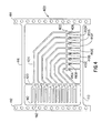
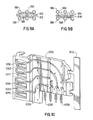
- FIG. 1 shows an exploded view of backplane assembly 100.
- Backplane 110 has pin header 114 attached to it.
- Daughter card 112 has daughter card connector 116 attached to it.
- Daughter card connector 116 can be mated to pin header 114 to form a connector.
- Backplane assembly likely has many other pin headers attached to it so that multiple daughter cards can be connected to it. Additionally, multiple pin headers might be aligned end to end so that multiple pin headers are used to connect to one daughter card. However, for clarity, only a portion of backplane assembly and a single daughter card 112 are shown.
- Pin header 114 is formed from shroud 120.
- Shroud 120 is preferably injection molded from a plastic, polyester or other suitable insulative material.
- Shroud 120 serves as the base for pin header 114.
- the floor (not numbered) of shroud 120 contains columns of holes 126.
- Pins 122 are inserted into holes 126 with their tails 124 extending through the lower surface of shroud 120. Tails 124 are pressed into signal holes 136.
- Holes 136 are plated through-holes in backplane 110 and serve to electrically connect pins 122 to traces (not shown) on backplane 110. For clarity of illustration, only a single pin 122 is shown. However, pin header 114 contains many parallel columns of pins. In a preferred embodiment, there are eight rows of pins in each column.
- each column of pins is not critical. However, it is one object of the invention to allow the pins to be placed close together so that a high density connector can be formed.
- the pins within each column can be spaced apart by 2.25 mm and the columns of pins can be spaced apart by 2mm.
- Pins 122 could be stamped from 0.4 mm thick copper alloy.
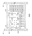
- Shroud 120 contains a groove 132 formed in its floor that runs parallel to the column of holes 126. Shroud 120 also has grooves 134 formed in its sidewalls. Shield plate 128 fits into grooves 132 and 134. Tails 130 protrude through holes (not visible) in the bottom of groove 132. Tails 130 engage ground holes 138 in backplane 110. Ground holes 138 are plated through-holes that connect to ground traces on backplane 110.
- plate 128 has seven tails 130. Each tail 130 falls between two adjacent pins 122. It would be desirable for shield 128 to have a tail 130 as close as possible to each pin 122. However, centering the tails 130 between adjacent signal pins 122 allows the spacing between shield 128 and a column of signal pins 122 to be reduced.
- Shield plate 128 has several torsional beams contacts 142 formed therein. Each contact 142 is formed by stamping arms 144 and 146 in plate 128. Arms 144 and 146 are then bent out of the plane plate 128. Arms 144 and 146 are long enough that they will flex when pressed back into the plane of plate 128. Arms 144 and 148 are sufficiently resilient to provide a spring force when pressed back into the plane of plate 128. The spring force generated by arms 144 and 146 creates a point of contact between each arm 144 or 146 and plate 150. The generated spring force must be sufficient to ensure this contact even after the daughter card connector 116 has been repeatedly mated and unmated from pin header 114.
- arms 144 and 146 are coined. Coining reduces the thickness of the material and increases the compliancy of the beams without weakening of plate 128.
- arms 144 and 146 be as short and straight as possible. Therefore, they are made only as long as needed to provide the required spring force.
- Grooves 140 on shroud 120 are for aligning daughter card connector 116 with pin header 114. Tabs 152 fit into grooves 140 for alignment and to prevent side to side motion of daughter card connector 116 relative to pin header 114.
- Daughter card connector 116 is made of wafers 154. Only one wafer 154 is shown for clarity, but daughter card connector 116 has, in a preferred embodiment, several wafers stacked side to side. Each wafer 154 contains one column of receptacles 158. Each receptacle 158 engages one pin 122 when the pin header 114 and daughter card connector 116 are mated. Thus, daughter card connector 116 is made from as many wafers as there are columns of pins in pin header 114.
- Stiffener 156 is preferably stamped and formed from a metal strip. It is stamped with features to hold wafer 154 in a required position without rotation and therefore preferably includes three attachment points. Stiffener 156 has slot 160A formed along its front edge. Tab 160B fits into slot 160A. Stiffener 156 also includes holes 162A and 164A. Hubs 162B and 164B fit into holes 162A and 164A. The hubs 162B and 164B are sized to provide an interference fit in holes 162A and 164A.
- FIG. 1 shows only a few of the slots 160A and holes 162A and 164A for clarity.
- the pattern of slots and holes is repeated along the length of stiffener 156 at each point where a wafer 156 is to be attached.
- wafer 154 is made in two pieces, shield piece 166 and signal piece 168.
- Shield piece 166 is formed by insert molding housing 170 around the front portion of shield 150.
- Signal piece 168 is made by insert molding housing 172 around contacts 410A...410H (FIG. 4).
- Signal piece 168 and shield piece 166 have features which hold the two pieces together.
- Signal piece 168 has hubs 512 (FIG. 5) formed on one surface. The hubs align with and are inserted into clips 174 cut into shield 150. Clips 174 engage hubs 512 and hold plate 150 firmly against signal piece 168.
- Housing 170 has cavities 176 formed in it. Each cavity 176 is shaped to receive one of the receptacles 158. Each cavity 176 has platform 178 at its bottom. Platform 178 has a hole 180 formed through it. Hole 180 receives a pin 122 when daughter card connector 116 mates with pin header 114. Thus, pins 122 mate with receptacles 158, providing a signal path through the connector.
- Receptacles 158 are formed with two legs 182. Legs 182 fit on opposite sides of platform 178 when receptacles 158 are inserted into cavities 176. Receptacles 158 are formed such that the spacing between legs 182 is smaller than the width of platform 178. To insert receptacles 158 into cavity 176, it is therefore necessary to use a tool to spread legs 182.
- the receptacles form what is known as a preloaded contact.
- Preloaded contacts have traditionally been formed by pressing the receptacle against a pyramid shaped platform. The apex of the platform spreads the legs as the receptacle is pushed down on it. Such a contact has a lower insertion force and is less likely to stub on the pin when the two connectors are mated.
- the receptacles of the invention provide the same advantages, but are achieved by inserting the receptacles from the side rather than by pressing them against a pyramid.
- Housing 172 has grooves 184 formed in it. As described above, hubs 512 (FIG. 5) project through plate 150. When two wafers are stacked side by side, hubs 512 from one wafer 154 will project into grooves 184 of an adjacent wafer. Hubs 512 and grooves 184 help hold adjacent wafers together and prevent rotation of one wafer with respect to the next. These features, in conjunction with stiffener 156 obviate the need for a separate box or housing to hold the wafers, thereby simplifying the connector.
- Housings 170 and 172 are shown with numerous holes (not numbered) in them. These holes are not critical to the invention. They are "pinch holes” used to hold plates 150 or receptacle contacts 410 during injection molding. It is desirable to hold these pieces during injection molding to maintain uniform spacing between the plates and receptacle contacts in the finished product.
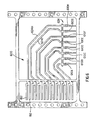
- FIG. 2 shows in greater detail the blank used to make plate 150.
- plates 150 are stamped from a roll of metal. The plates are retained on carrier strip 210 for ease of handling. After plate 150 is injection molded into a shield piece 166, the carrier strip can be cut off.
- Plates 150 include holes 212. Holes 212 are filled with plastic from housing 170, thereby locking plate 150 in housing 170.
- Plates 150 also include slots 214. Slots 214 are positioned to fall between receptacles 158. Slots 214 serve to control the capacitance of plate 150, which can overall raise or lower the impedance of the connector. They also channel current flow in the plate near receptacles 158, which are the signal paths. Higher return current flow near the signal paths reduces cross talk.
- Slot 216 is similar to the slots 214, but is larger to allow a finger 316 (FIG. 3) to pass through plate 150 when plate 150 is molded into a housing 170.
- Finger 316 is a small finger of insulating material that could aid in holding a plate 128 against plate 150. Finger 316 is optional and could be omitted. Note in FIG. 1 that the central two cavities 176 have their intermediate wall partially removed. Finger 316 from an adjacent wafer 154 (not shown) would fit into this space to complete the wall between the two central cavities. Finger 316 would extend beyond housing 170 and would fit into a slot 184B of an adjacent wafer (not shown).
- FIG. 9A shows traces 910 and 912 on a printed circuit board routed between holes used to mount a connector according to the invention.
- FIG. 9A shows portions of a column of signal holes 186 and portions of a column of ground contacts 188.
- the traces 910 and 912 be separated by ground to the greatest extent possible.
- the ground holes 188 be centered between the column of signal holes 186 so that the signal traces 910 and 912 can be routed between the signal holes 186 and ground holes 188.
- FIG. 9B shows the preferred routing for differential pair signals.
- the traces be routed as close together as possible.
- the ground holes 188 are not centered between columns of signal holes 186. Rather, they are offset to be as close to one row of signal contacts 186. That placement allows both signal traces 914 and 916 to be routed between the ground holes 188 and a column of signal holes 186.
- tail region 222 is bent out of the plane of plate 150. For the differential configuration, it is not bent.
- plate 128 (FIG. 1) can be similarly bent in its tail region, if desired. In the preferred embodiment, though, plate 128 is not bent for single ended signals and is bent for differential signals.
- Tabs 220 are bent out of the plane of plate 150 prior to injection molding of the housing 170. Tabs 220 will wind up between holes 180 (FIG. 1). Tabs 220 aid in assuring that plate 150 adheres to housing 170. They also reinforce housing 170 across its face, i.e. that surface facing pin header 114.
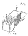
- FIG. 3 shows shield 150 after it has been insert molded into housing 170 to form ground portion 166.
- housing 170 includes pyramid shaped projections 310 on the face of shield piece 166.
- Matching recesses (not shown) are included in the floor of pin header 114. Projections 310 and the matching recesses serve to prevent the spring force of torsional beam contacts 142 from spreading adjacent wafers 154 when daughter card connector 116 is inserted into pin header 114.
- FIG. 4 shows receptacle contact blank 400.
- Receptacle contact blank is preferably stamped from a sheet of metal. Numerous such blanks are stamped in a roll.
- the receptacle contacts 410 are held together on carrier strips 412, 414, 416, 418 and 422. These carrier strips are severed to separate contacts 410A....410H after housing 172 has been molded around the contacts.
- the carrier strips can be retained during much of the manufacturing operation for easy handling of receptacle portions 168.
- Each of the receptacle contacts 410A...410H includes two legs 182.
- the legs 182 are folded and bent to form the receptacle 158.
- Each receptacle contact 410A...410H also includes a transmission region 424 and a tail region 426.
- FIG. 4 shows that the transmission regions 424 are equally spaced. This arrangement is preferred for single ended signals as it results in maximum spacing between the contacts.
- FIG. 4 shows that the tail regions are suitable for being press fit into plated through-holes.
- Other types of tail regions might be used.
- solder tails might be used instead.
- FIG. 5 shows receptacle contact blank 400 after housing 172 has been molded around it.
- FIG. 6 shows a receptacle contact blank 600 suitable for use in an alternative embodiment of the invention.
- Receptacle contacts 610A...610H are grouped in pairs: (610A and 610B), (610C and 610D), (610E and 610F) and (610G and 610H).
- Transmission regions 624 of each pair are as close together as possible while maintaining differential impedance. This increases the spacing between adjacent pairs. This configuration improves the signal integrity for differential signals.
- tail region 626 and the receptacles of receptacle contact blank 400 and 600 are identical. These are the only portions of receptacle contacts 410 and 610 extending from housing 172. Thus, externally, signal portion 168 is the same for either single ended or differential signals. This allows single ended and differential signal wafers to be mixed in a single daughter card connector.
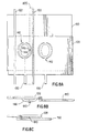
- FIG. 7A illustrates a prior art connector as an aid in explaining the improved performance of the invention.
- FIG. 7A shows a shield plate 710 with a cantilevered beam 712 formed in it.
- the cantilevered beam 712 engages a blade 714 from the pin header.
- the point of contact is labeled X.
- Blade 714 is connected to a backplane (not shown) at point 722.
- Signals are transmitted through signal pins 716 and 718 running adjacent to the shield plate. Plate 710 and blade 714 act as the signal return.
- the signal path 720 through these elements is shown as a loop. It should be noted that signal path 720 cuts through pin 718.
- a signal traveling in a loop passing through a conductor will inductively couple to the conductor.
- the arrangement of FIG. 7A will have relatively high coupling or cross talk from pin 716 to 718.
- FIG. 7B shows a side view of the arrangement of FIG. 7A.
- the cantilevered beam 712 is above the blade 714 its distance from pin 716 is d 1 .
- blade 714 has a spacing of d 2 , which is larger.
- d 1 the distance between the signal path and the ground dictates the impedance of the signal path. Changes in distance mean changes in impedance. Changes in impedance cause signal reflections, which is undesirable.
- FIG. 7C shows the same arrangement upon mating.
- the blade 714 must slide under cantilevered beam 712. If not inserted correctly, blade 714 can but up against the end of cantilevered beam 712. This phenomenon is called “stubbing.” It is highly undesirable in a connector because it can break the connector.
- FIG. 8 shows in a schematic sense the components of a connector manufactured according to the invention. Shield plates 128 and 150 overlap. Contact is made at the point marked X on torsional beam 146. Signal path 820 is shown to pass through a signal pin 122, return through plate 150 to point of contact X, pass through arm 146, through plate 128 and through tail 130. Signal path 820 is then completed through the backplane (not shown in FIG. 8). Significantly, signal path 820 does not cut through any adjacent signal pin 122. In this way, cross talk is significantly reduced over the prior art.
- FIG. 8B illustrates schematically plates 128 and 150 prior to mating of daughter card connector 116 to pin header 114.
- arm 146 is shown bent out of the plane of plate 128. As plates 150 and 128 slide along one another during mating, arm 146 is pressed back into the plane of plate 128.
- FIG. 8C show plates 128 and 150 in the mated configuration. Dimple 810 pressed into arm 146 is shown touching plate 150. The torsional spring force generated by pressing arm 146 back into the plane of plate 128 ensures a good electrical contact. It should be noted that the spacing between the plates 128 or 150 and an adjacent signal contact do not have as large a discontinuity as shown in FIG. 7B. This improvement should improve the electrical performance of the connector.
- FIG. 10 shows an alternative embodiment of a wafer 154 (FIG. 1).
- a shield blank on carrier strip 1010 is encapsulated in an insulative housing 1070 through injection molding. Shield tails 1030 are shown extending from housing 1070.
- Housing 1070 includes cavities 1016, 1017, 1018 and 1019. The shield blank is cut and bent to make contacts 1020 within cavities 1016, 1017, 1018 and 1019.
- Cavities 1016, 1017, 1018 and 1019 have holes 1022 formed in their floors. Pins from the pin header are inserted through the holes during mating and engage, through the springiness of the pin as well as of contacts 1020 ensure electrical connection to the shield.
- the signal contacts are stamped separately.
- the transmission line section of the contacts are laid into cavities 1026.
- the receptacle portions of the signal contacts are inserted into cavities 1024.
- a wafer as in FIG. 10 illustrates that any number of signal contacts might be used per column. In FIG. 10, four signal contacts per column are shown. That figure also illustrates that pins might be used in place of a plate 128. However, there might be differences in electrical performance.
- a plate could be used in conjunction with the configuration of FIG. 10. In that case, instead of a series of separate holes 1022 in cavities 1016, 1017, 1018 and 1019, a slot would be cut through the cavities.
- FIG. 11A shows an alternative embodiment for contacts 142 on plate 128.
- Plate 1128 includes a series of torsional contacts 142. Each contact is made by stamping an arm 1146 from plate 1128.
- the arms have a generally serpentine shape. As described above, it is desirable for the arms 146 to be long enough to provide good flexibility. However, it is also desirable for the current to flow through the contacts 1142 in an area that is as narrow as possible in a direction perpendicular to the flow of current through signal pins 122. To achieve both of these goals, arms 1146 are stamped in a serpentine shape.
- FIG. 11B shows plate 1128 in cross section through the line indicated as B-B in FIG. 1A. As shown, arms 1146 are bent out of the plane of plate 1128. During mating of the connector half, they are pressed back into the plane of plate 1128, thereby generating a torsional force.
- Fig. 12 shows an additional view of connector 100.
- Fig. 12 shows face 1210 of daughter card connector 116.
- the lower surface of pin header 114 is also visible.
- the press fit tails 124 of plate 128 have an orientation that is at right angles to the orientation of press fit tails 130 of signal pins 122.
- a connector made according to the invention was made and tested. The test was made with the single ended configuration and measurements were made on one signal line with the ten closest lines driven. For signal rise times of 500ps, the backward crosstalk was 4.9%. The forward cross talk was 3.2%. The reflection was too small to measure.
- the connector provided a real signal density of approximately 4 per linear millimetre (101 per linear inch).
- clips 174 are shown generally to be radially symmetrical. It might improve the effectiveness of the shield plate 150 if clips 174 were elongated with a major axis running parallel with the signal contacts in signal pieces 168 and a perpendicular minor axis which is as short as possible.
- daughter card connector 116 is formed by organizing a plurality of wafers onto a stiffener. It might be possible that an equivalent structure might be formed by inserting a plurality of shield pieces and signal receptacles into a molded housing.
Description
Claims (12)
- An electrical connector with a first connector piece (114) having a plurality of columns of first signal contacts (122) and a second connector piece (116) having columns of second signal contacts (158) adapted to mate to the first signal contacts when the first connector piece and the second connector piece are mated, the connector further comprising:a) a first plurality of shield plates (128), each disposed between adjacent rows of said first signal contacts in the first connector piece;b) a second plurality of shield plates (150), each disposed between adjacent rows of said second signal contacts in the second connector piece; and
CHARACTERIZED IN THAT the connector further comprises:c) a plurality of torsional contacts (142) on the first plurality or second plurality of shield plates, each torsional contact comprises an arm (144 or 146) having two ends attached to one of the shield plates, when not mated a said torsional contact being bent out of the plane of the plate, and wherein when the first connector piece and the second connector piece are mated, each of the first plurality of plates makes contact to one of the second plurality of plates at a plurality of points. - The electrical connector of claim 1 wherein the first connector piece comprises a pin header (114) having a plurality of rows of signal pins (122) mounted in a shroud (120) having two side walls with slots (134) formed therein and the first plurality of shield plates engage the slots on the side walls.
- The electrical connector of claim 1 wherein a said arm has a thickness less than the thickness of the shield plate to which it is attached.
- The electrical connector of claim 1 wherein a said arm has a serpentine shape.
- The electrical connector of claim 1 wherein each of said second plurality of shield plates includes slots (214) positioned to lie between said signal contacts (158).
- The electrical connector of claim 1 wherein a shield plate (150) of said second plurality of shield plates has a housing (170), the housing (170) and the shield plate (150) comprising a shield piece (166), the housing (170) including pyramid shaped projections (310) on the face of the shield piece; and
wherein the first connector piece (114) includes matching recesses in a floor portion of the piece. - The electrical connector according to any of the preceding claims wherein each of the signal contacts has a tail (124; 426) and each of the shield plates has a plurality of tails (130; 1030) disposed between adjacent signal contact tails.
- An electrical connector according to any of the preceding claims wherein the second connector piece (116) comprises a plurality of wafers (154) aligned in parallel with each of the second plurality of shields (150) accessible from a side of one of the wafers, the wafers being positioned such that, when the first connector piece and the second connector piece are mated, the first plurality of shields (128) fit between adjacent wafers to make contact with one of the second plurality of shields.
- An electrical connector according to any of claims 1 through 3 additionally comprising:a) a stiffener (156);b) a plurality of wafers (154), each of the wafers having a front face (1210) facing the first connector piece and a rear portion attached to the stiffener, thereby leaving slots between the front faces of adjacent wafers, wherein the first plurality of shield plates are inserted into the slots.
- An electrical connector according to claim 8 or 9 wherein each of the wafers includes one column of signal contacts secured in an housing (172).
- The electrical connector according to any of the preceding claims wherein the signal contacts in the second connector piece comprise receptacle contacts.
- An electrical connector according to any of the preceding claims wherein the first connector piece is attached to a backplane (110) and the second connector piece is attached to a daughter card (112).
Applications Claiming Priority (3)
| Application Number | Priority Date | Filing Date | Title |
|---|---|---|---|
| US08/797,537 US5993259A (en) | 1997-02-07 | 1997-02-07 | High speed, high density electrical connector |
| US797537 | 1997-02-07 | ||
| PCT/US1998/001168 WO1998035409A1 (en) | 1997-02-07 | 1998-01-15 | High speed, high density electrical connector |
Publications (2)
| Publication Number | Publication Date |
|---|---|
| EP1021854A1 EP1021854A1 (en) | 2000-07-26 |
| EP1021854B1 true EP1021854B1 (en) | 2003-05-02 |
Family
ID=25171119
Family Applications (1)
| Application Number | Title | Priority Date | Filing Date |
|---|---|---|---|
| EP98902829A Expired - Lifetime EP1021854B1 (en) | 1997-02-07 | 1998-01-15 | High speed, high density electrical connector |
Country Status (8)
| Country | Link |
|---|---|
| US (5) | US5993259A (en) |
| EP (1) | EP1021854B1 (en) |
| JP (1) | JP2001510627A (en) |
| KR (1) | KR100517158B1 (en) |
| CA (1) | CA2280173C (en) |
| DE (1) | DE69814123T2 (en) |
| IL (1) | IL131286A0 (en) |
| WO (1) | WO1998035409A1 (en) |
Cited By (1)
| Publication number | Priority date | Publication date | Assignee | Title |
|---|---|---|---|---|
| CN106058544A (en) * | 2016-08-03 | 2016-10-26 | 欧品电子(昆山)有限公司 | High speed connector assembly, socket connector and plug connector |
Families Citing this family (338)
| Publication number | Priority date | Publication date | Assignee | Title |
|---|---|---|---|---|
| US6179663B1 (en) * | 1998-04-29 | 2001-01-30 | Litton Systems, Inc. | High density electrical interconnect system having enhanced grounding and cross-talk reduction capability |
| US6231391B1 (en) | 1999-08-12 | 2001-05-15 | Robinson Nugent, Inc. | Connector apparatus |
| ATE316699T1 (en) * | 1998-08-12 | 2006-02-15 | Robinson Nugent Inc | CONNECTING DEVICE |
| US6530790B1 (en) * | 1998-11-24 | 2003-03-11 | Teradyne, Inc. | Electrical connector |
| US6171149B1 (en) * | 1998-12-28 | 2001-01-09 | Berg Technology, Inc. | High speed connector and method of making same |
| US6267625B1 (en) | 1999-04-21 | 2001-07-31 | Litton Systems, Inc. | High density electrical interconnect system having enhanced grounding and cross-talk reduction capability |
| JP2001015223A (en) * | 1999-06-25 | 2001-01-19 | Nec Corp | Versatile connector and its coupling method |
| US6565387B2 (en) * | 1999-06-30 | 2003-05-20 | Teradyne, Inc. | Modular electrical connector and connector system |
| US6494743B1 (en) | 1999-07-02 | 2002-12-17 | General Dynamics Information Systems, Inc. | Impedance-controlled connector |
| US6168469B1 (en) * | 1999-10-12 | 2001-01-02 | Hon Hai Precision Ind. Co., Ltd. | Electrical connector assembly and method for making the same |
| JP2001167839A (en) * | 1999-12-01 | 2001-06-22 | Molex Inc | Electrical connector assembly |
| US6172895B1 (en) * | 1999-12-14 | 2001-01-09 | High Connector Density, Inc. | High capacity memory module with built-in-high-speed bus terminations |
| US6171115B1 (en) * | 2000-02-03 | 2001-01-09 | Tyco Electronics Corporation | Electrical connector having circuit boards and keying for different types of circuit boards |
| WO2001057963A2 (en) | 2000-02-03 | 2001-08-09 | Teradyne, Inc. | High speed pressure mount connector |
| US6267604B1 (en) * | 2000-02-03 | 2001-07-31 | Tyco Electronics Corporation | Electrical connector including a housing that holds parallel circuit boards |
| US6371788B1 (en) | 2000-05-19 | 2002-04-16 | Molex Incorporated | Wafer connection latching assembly |
| US6273758B1 (en) | 2000-05-19 | 2001-08-14 | Molex Incorporated | Wafer connector with improved grounding shield |
| DE10027556C1 (en) * | 2000-06-02 | 2001-11-29 | Harting Kgaa | PCB connector |
| US6354885B1 (en) | 2000-06-05 | 2002-03-12 | Northrop Grumman Corporation | Guide system with integral keying and electrostatic discharge paths for separable pin and socket connector systems |
| AU2001271371A1 (en) | 2000-06-29 | 2002-01-14 | Robinson Nugent, Inc. | High speed connector |
| US6780058B2 (en) * | 2000-10-17 | 2004-08-24 | Molex Incorporated | Shielded backplane connector |
| JP3491064B2 (en) * | 2000-10-20 | 2004-01-26 | 日本航空電子工業株式会社 | High-speed transmission connector |
| US6843657B2 (en) * | 2001-01-12 | 2005-01-18 | Litton Systems Inc. | High speed, high density interconnect system for differential and single-ended transmission applications |
| US7040901B2 (en) * | 2001-01-12 | 2006-05-09 | Litton Systems, Inc. | High-speed electrical connector |
| US6979202B2 (en) * | 2001-01-12 | 2005-12-27 | Litton Systems, Inc. | High-speed electrical connector |
| US6592381B2 (en) * | 2001-01-25 | 2003-07-15 | Teradyne, Inc. | Waferized power connector |
| US6409543B1 (en) * | 2001-01-25 | 2002-06-25 | Teradyne, Inc. | Connector molding method and shielded waferized connector made therefrom |
| US6461202B2 (en) * | 2001-01-30 | 2002-10-08 | Tyco Electronics Corporation | Terminal module having open side for enhanced electrical performance |
| US6769935B2 (en) | 2001-02-01 | 2004-08-03 | Teradyne, Inc. | Matrix connector |
| IL142157A (en) | 2001-03-21 | 2008-03-20 | Rit Techn Ltd | Patch panel |
| US6836810B1 (en) * | 2001-03-29 | 2004-12-28 | Fairchild Semiconductor Corporation | Backplane system using incident waveform switching |
| US6551140B2 (en) * | 2001-05-09 | 2003-04-22 | Hon Hai Precision Ind. Co., Ltd. | Electrical connector having differential pair terminals with equal length |
| US6439930B1 (en) * | 2001-11-05 | 2002-08-27 | Hon Hai Precision Ind. Co., Ltd. | Electrical connector configured by wafers including moveable contacts |
| NL1018175C2 (en) * | 2001-05-30 | 2002-12-03 | Fci Mechelen N V | Plug block and cable connector. |
| US6608762B2 (en) | 2001-06-01 | 2003-08-19 | Hyperchip Inc. | Midplane for data processing apparatus |
| US6435914B1 (en) * | 2001-06-27 | 2002-08-20 | Hon Hai Precision Ind. Co., Ltd. | Electrical connector having improved shielding means |
| US6869292B2 (en) | 2001-07-31 | 2005-03-22 | Fci Americas Technology, Inc. | Modular mezzanine connector |
| WO2003067711A2 (en) * | 2001-10-10 | 2003-08-14 | Molex Incorporated | High speed differential signal edge card connector circuit board layouts |
| US20050178884A1 (en) * | 2001-11-06 | 2005-08-18 | Konrad Schafroth | Flight device with a lift-generating fuselage |
| US6652318B1 (en) * | 2002-05-24 | 2003-11-25 | Fci Americas Technology, Inc. | Cross-talk canceling technique for high speed electrical connectors |
| US6692272B2 (en) | 2001-11-14 | 2004-02-17 | Fci Americas Technology, Inc. | High speed electrical connector |
| US7390200B2 (en) * | 2001-11-14 | 2008-06-24 | Fci Americas Technology, Inc. | High speed differential transmission structures without grounds |
| US6976886B2 (en) * | 2001-11-14 | 2005-12-20 | Fci Americas Technology, Inc. | Cross talk reduction and impedance-matching for high speed electrical connectors |
| US20050196987A1 (en) | 2001-11-14 | 2005-09-08 | Shuey Joseph B. | High density, low noise, high speed mezzanine connector |
| US6981883B2 (en) * | 2001-11-14 | 2006-01-03 | Fci Americas Technology, Inc. | Impedance control in electrical connectors |
| US6994569B2 (en) * | 2001-11-14 | 2006-02-07 | Fci America Technology, Inc. | Electrical connectors having contacts that may be selectively designated as either signal or ground contacts |
| US6979215B2 (en) * | 2001-11-28 | 2005-12-27 | Molex Incorporated | High-density connector assembly with flexural capabilities |
| US20030133276A1 (en) * | 2002-01-17 | 2003-07-17 | Dong Zhong | Arrangements to improve noise immunity of differential signals |
| US6739918B2 (en) * | 2002-02-01 | 2004-05-25 | Teradyne, Inc. | Self-aligning electrical connector |
| US6743057B2 (en) * | 2002-03-27 | 2004-06-01 | Tyco Electronics Corporation | Electrical connector tie bar |
| US6764349B2 (en) * | 2002-03-29 | 2004-07-20 | Teradyne, Inc. | Matrix connector with integrated power contacts |
| US6843686B2 (en) * | 2002-04-26 | 2005-01-18 | Honda Tsushin Kogyo Co., Ltd. | High-frequency electric connector having no ground terminals |
| JP2006515705A (en) * | 2002-05-06 | 2006-06-01 | モレックス インコーポレーテッド | Differential signal connector with electrostatic discharge protection function |
| EP1504498B1 (en) * | 2002-05-10 | 2008-12-10 | Molex Incorporated | Edge card connector assembly with tuned impedance terminals |
| US6638079B1 (en) * | 2002-05-21 | 2003-10-28 | Hon Hai Precision Ind. Co., Ltd. | Customizable electrical connector |
| US6623310B1 (en) * | 2002-05-21 | 2003-09-23 | Hon Hai Precision Ind. Co., Ltd. | High density electrical connector assembly with reduced insertion force |
| US6638110B1 (en) * | 2002-05-22 | 2003-10-28 | Hon Hai Precision Ind. Co., Ltd. | High density electrical connector |
| US6743049B2 (en) * | 2002-06-24 | 2004-06-01 | Advanced Interconnections Corporation | High speed, high density interconnection device |
| US6796822B2 (en) * | 2002-07-02 | 2004-09-28 | Fujitsu Component Limited | Contact module and connector having the same |
| US6905367B2 (en) | 2002-07-16 | 2005-06-14 | Silicon Bandwidth, Inc. | Modular coaxial electrical interconnect system having a modular frame and electrically shielded signal paths and a method of making the same |
| US7270573B2 (en) * | 2002-08-30 | 2007-09-18 | Fci Americas Technology, Inc. | Electrical connector with load bearing features |
| US7008250B2 (en) * | 2002-08-30 | 2006-03-07 | Fci Americas Technology, Inc. | Connector receptacle having a short beam and long wipe dual beam contact |
| US6682369B1 (en) * | 2002-09-18 | 2004-01-27 | Hon Hai Precision Ind. Co., Ltd. | Electrical connector having retention system for precisely mounting plural boards therein |
| US6880243B2 (en) * | 2002-10-04 | 2005-04-19 | Sanmina-Sci Corporation | Stiffener for stiffening a circuit board |
| US6695646B1 (en) * | 2002-10-18 | 2004-02-24 | Hon Hai Precision Ind. Co., Ltd. | Electrical connector having floatable chicklets |
| US6685510B1 (en) * | 2002-10-22 | 2004-02-03 | Hon Hai Precision Ind. Co., Ltd. | Electrical cable connector |
| US20050026506A1 (en) * | 2002-11-18 | 2005-02-03 | Trompeter Electronics, Inc. | Modular cross-connect with hot-swappable modules |
| US6752665B2 (en) * | 2002-11-18 | 2004-06-22 | Trompeter Electronics, Inc. | Modular cross-connect with removable switch assembly |
| US6808399B2 (en) * | 2002-12-02 | 2004-10-26 | Tyco Electronics Corporation | Electrical connector with wafers having split ground planes |
| CN100524954C (en) * | 2002-12-04 | 2009-08-05 | 莫莱克斯公司 | High-density connector assembly with tracking ground structure |
| US6743050B1 (en) * | 2002-12-10 | 2004-06-01 | Hon Hai Precision Ind. Co., Ltd. | Cable assembly with latch mechanism |
| US6786771B2 (en) * | 2002-12-20 | 2004-09-07 | Teradyne, Inc. | Interconnection system with improved high frequency performance |
| US20040147169A1 (en) | 2003-01-28 | 2004-07-29 | Allison Jeffrey W. | Power connector with safety feature |
| DE10310502A1 (en) * | 2003-03-11 | 2004-09-23 | Molex Inc., Lisle | Earthed electrical connector for GHz signal frequency range, has earthing terminal provided with at least 2 mechanically coupled electrical contacts |
| US7018246B2 (en) * | 2003-03-14 | 2006-03-28 | Fci Americas Technology, Inc. | Maintenance of uniform impedance profiles between adjacent contacts in high speed grid array connectors |
| JP4212955B2 (en) * | 2003-05-27 | 2009-01-21 | 富士通コンポーネント株式会社 | Plug connector for balanced transmission |
| US6827611B1 (en) | 2003-06-18 | 2004-12-07 | Teradyne, Inc. | Electrical connector with multi-beam contact |
| JP4590406B2 (en) * | 2003-07-17 | 2010-12-01 | ウィンチェスター・エレクトロニクス・コーポレイション | High speed electrical connector |
| US7083432B2 (en) * | 2003-08-06 | 2006-08-01 | Fci Americas Technology, Inc. | Retention member for connector system |
| US6884117B2 (en) * | 2003-08-29 | 2005-04-26 | Hon Hai Precision Ind. Co., Ltd. | Electrical connector having circuit board modules positioned between metal stiffener and a housing |
| US6808419B1 (en) * | 2003-08-29 | 2004-10-26 | Hon Hai Precision Ind. Co., Ltd. | Electrical connector having enhanced electrical performance |
| US6811440B1 (en) | 2003-08-29 | 2004-11-02 | Tyco Electronics Corporation | Power connector |
| US7074086B2 (en) * | 2003-09-03 | 2006-07-11 | Amphenol Corporation | High speed, high density electrical connector |
| US6866518B1 (en) | 2003-09-23 | 2005-03-15 | Hon Hai Precision Ind. Co., Ltd. | Electrical interconnection between multiple printed circuit boards |
| US6923655B2 (en) * | 2003-09-23 | 2005-08-02 | Hon Hai Precision Ind. Co., Ltd. | Electrical connector for interconnecting two intersected printed circuit boards |
| US6918775B2 (en) * | 2003-09-23 | 2005-07-19 | Hon Hai Precision Ind. Co., Ltd. | Method for interconnecting multiple printed circuit boards |
| US7524209B2 (en) | 2003-09-26 | 2009-04-28 | Fci Americas Technology, Inc. | Impedance mating interface for electrical connectors |
| WO2005031922A2 (en) * | 2003-09-26 | 2005-04-07 | Fci Americas Technology, Inc. | Improved impedance mating interface for electrical connectors |
| US6875031B1 (en) * | 2003-12-05 | 2005-04-05 | Hon Hai Precision Ind. Co., Ltd. | Electrical connector with circuit board module |
| EP1702389B1 (en) | 2003-12-31 | 2020-12-09 | Amphenol FCI Asia Pte. Ltd. | Electrical power contacts and connectors comprising same |
| US7458839B2 (en) | 2006-02-21 | 2008-12-02 | Fci Americas Technology, Inc. | Electrical connectors having power contacts with alignment and/or restraining features |
| EP1721496A2 (en) * | 2004-02-13 | 2006-11-15 | Molex Incorporated | Preferential ground and via exit structures for printed circuit boards |
| EP1841298A3 (en) * | 2004-02-13 | 2008-05-07 | Molex Incorporated | Plated vias exit structure for printed circuit board |
| US20050201065A1 (en) * | 2004-02-13 | 2005-09-15 | Regnier Kent E. | Preferential ground and via exit structures for printed circuit boards |
| US6932649B1 (en) * | 2004-03-19 | 2005-08-23 | Tyco Electronics Corporation | Active wafer for improved gigabit signal recovery, in a serial point-to-point architecture |
| US7137832B2 (en) * | 2004-06-10 | 2006-11-21 | Samtec Incorporated | Array connector having improved electrical characteristics and increased signal pins with decreased ground pins |
| US7285018B2 (en) * | 2004-06-23 | 2007-10-23 | Amphenol Corporation | Electrical connector incorporating passive circuit elements |
| US7108556B2 (en) * | 2004-07-01 | 2006-09-19 | Amphenol Corporation | Midplane especially applicable to an orthogonal architecture electronic system |
| US7094102B2 (en) | 2004-07-01 | 2006-08-22 | Amphenol Corporation | Differential electrical connector assembly |
| US8444436B1 (en) | 2004-07-01 | 2013-05-21 | Amphenol Corporation | Midplane especially applicable to an orthogonal architecture electronic system |
| US7242325B2 (en) * | 2004-08-02 | 2007-07-10 | Sony Corporation | Error correction compensating ones or zeros string suppression |
| US7160117B2 (en) * | 2004-08-13 | 2007-01-09 | Fci Americas Technology, Inc. | High speed, high signal integrity electrical connectors |
| US7182642B2 (en) * | 2004-08-16 | 2007-02-27 | Fci Americas Technology, Inc. | Power contact having current flow guiding feature and electrical connector containing same |
| JP2006073555A (en) | 2004-08-31 | 2006-03-16 | Hirose Electric Co Ltd | Transmission circuit board structure, transmission circuit board and connector having the same |
| US7214104B2 (en) * | 2004-09-14 | 2007-05-08 | Fci Americas Technology, Inc. | Ball grid array connector |
| US7359214B2 (en) * | 2004-09-28 | 2008-04-15 | Amphenol Corporation | Backplane with routing to reduce layer count |
| US7281950B2 (en) * | 2004-09-29 | 2007-10-16 | Fci Americas Technology, Inc. | High speed connectors that minimize signal skew and crosstalk |
| US7090512B2 (en) * | 2004-10-15 | 2006-08-15 | Tyco Electronics Corporatin | Connector system for conductive plates |
| WO2006047425A2 (en) * | 2004-10-25 | 2006-05-04 | Intrado, Inc. | System and method for unilateral verification of caller location information |
| EP1810552A1 (en) | 2004-10-29 | 2007-07-25 | Molex Incorporated | Printed circuit board for high-speed electrical connectors |
| US20060162960A1 (en) * | 2004-12-16 | 2006-07-27 | Litton Systems, Inc. | System for determining printed circuit board passive channel losses |
| US7476108B2 (en) * | 2004-12-22 | 2009-01-13 | Fci Americas Technology, Inc. | Electrical power connectors with cooling features |
| US7226296B2 (en) * | 2004-12-23 | 2007-06-05 | Fci Americas Technology, Inc. | Ball grid array contacts with spring action |
| US20060151869A1 (en) * | 2005-01-10 | 2006-07-13 | Franz Gisin | Printed circuit boards and the like with improved signal integrity for differential signal pairs |
| US7104808B2 (en) * | 2005-01-20 | 2006-09-12 | Hon Hai Precision Ind. Co., Ltd. | Mating extender for electrically connecting with two electrical connectors |
| US7384289B2 (en) | 2005-01-31 | 2008-06-10 | Fci Americas Technology, Inc. | Surface-mount connector |
| US7131870B2 (en) * | 2005-02-07 | 2006-11-07 | Tyco Electronics Corporation | Electrical connector |
| WO2006091595A1 (en) * | 2005-02-22 | 2006-08-31 | Molex Incorporated | Differential signal connector with wafer-style construction |
| US7090501B1 (en) * | 2005-03-22 | 2006-08-15 | 3M Innovative Properties Company | Connector apparatus |
| US7175446B2 (en) * | 2005-03-28 | 2007-02-13 | Tyco Electronics Corporation | Electrical connector |
| US7303427B2 (en) | 2005-04-05 | 2007-12-04 | Fci Americas Technology, Inc. | Electrical connector with air-circulation features |
| US20060228912A1 (en) * | 2005-04-07 | 2006-10-12 | Fci Americas Technology, Inc. | Orthogonal backplane connector |
| US20060245137A1 (en) * | 2005-04-29 | 2006-11-02 | Fci Americas Technology, Inc. | Backplane connectors |
| US6986682B1 (en) | 2005-05-11 | 2006-01-17 | Myoungsoo Jeon | High speed connector assembly with laterally displaceable head portion |
| EP1732176A1 (en) * | 2005-06-08 | 2006-12-13 | Tyco Electronics Nederland B.V. | Electrical connector |
| US7396259B2 (en) * | 2005-06-29 | 2008-07-08 | Fci Americas Technology, Inc. | Electrical connector housing alignment feature |
| US7163421B1 (en) * | 2005-06-30 | 2007-01-16 | Amphenol Corporation | High speed high density electrical connector |
| US20090291593A1 (en) | 2005-06-30 | 2009-11-26 | Prescott Atkinson | High frequency broadside-coupled electrical connector |
| US8083553B2 (en) * | 2005-06-30 | 2011-12-27 | Amphenol Corporation | Connector with improved shielding in mating contact region |
| US7914304B2 (en) | 2005-06-30 | 2011-03-29 | Amphenol Corporation | Electrical connector with conductors having diverging portions |
| US8189599B2 (en) * | 2005-08-23 | 2012-05-29 | Rpx Corporation | Omni-protocol engine for reconfigurable bit-stream processing in high-speed networks |
| US7494379B2 (en) * | 2005-09-06 | 2009-02-24 | Amphenol Corporation | Connector with reference conductor contact |
| US7331802B2 (en) * | 2005-11-02 | 2008-02-19 | Tyco Electronics Corporation | Orthogonal connector |
| US7819708B2 (en) * | 2005-11-21 | 2010-10-26 | Fci Americas Technology, Inc. | Receptacle contact for improved mating characteristics |
| US7827442B2 (en) * | 2006-01-23 | 2010-11-02 | Slt Logic Llc | Shelf management controller with hardware/software implemented dual redundant configuration |
| US7270574B1 (en) * | 2006-02-07 | 2007-09-18 | Fci Americas Technology, Inc. | Covers for electrical connectors |
| US7431616B2 (en) * | 2006-03-03 | 2008-10-07 | Fci Americas Technology, Inc. | Orthogonal electrical connectors |
| US7331830B2 (en) * | 2006-03-03 | 2008-02-19 | Fci Americas Technology, Inc. | High-density orthogonal connector |
| US7407413B2 (en) * | 2006-03-03 | 2008-08-05 | Fci Americas Technology, Inc. | Broadside-to-edge-coupling connector system |
| US20070207632A1 (en) * | 2006-03-03 | 2007-09-06 | Fci Americas Technology, Inc. | Midplane with offset connectors |
| US7344391B2 (en) * | 2006-03-03 | 2008-03-18 | Fci Americas Technology, Inc. | Edge and broadside coupled connector |
| US7393249B2 (en) | 2006-04-21 | 2008-07-01 | Trompeter Electronics, Inc. | Interconnection and monitoring module |
| US7264509B1 (en) * | 2006-04-24 | 2007-09-04 | Tyco Electronics Corporation | Modular connector assembly utilizing a generic lead frame |
| US7261580B1 (en) | 2006-04-27 | 2007-08-28 | General Electric Company | Cable connector |
| US7425145B2 (en) * | 2006-05-26 | 2008-09-16 | Fci Americas Technology, Inc. | Connectors and contacts for transmitting electrical power |
| US7316585B2 (en) * | 2006-05-30 | 2008-01-08 | Fci Americas Technology, Inc. | Reducing suck-out insertion loss |
| US7726982B2 (en) | 2006-06-15 | 2010-06-01 | Fci Americas Technology, Inc. | Electrical connectors with air-circulation features |
| US7462924B2 (en) * | 2006-06-27 | 2008-12-09 | Fci Americas Technology, Inc. | Electrical connector with elongated ground contacts |
| US7318757B1 (en) | 2006-06-30 | 2008-01-15 | Fci Americas Technology, Inc. | Leadframe assembly staggering for electrical connectors |
| US7309257B1 (en) * | 2006-06-30 | 2007-12-18 | Fci Americas Technology, Inc. | Hinged leadframe assembly for an electrical connector |
| US7632149B2 (en) * | 2006-06-30 | 2009-12-15 | Molex Incorporated | Differential pair connector featuring reduced crosstalk |
| US7413484B2 (en) * | 2006-08-02 | 2008-08-19 | Tyco Electronics Corporation | Electrical terminal having a compliant retention section |
| US7753742B2 (en) | 2006-08-02 | 2010-07-13 | Tyco Electronics Corporation | Electrical terminal having improved insertion characteristics and electrical connector for use therewith |
| US7591655B2 (en) * | 2006-08-02 | 2009-09-22 | Tyco Electronics Corporation | Electrical connector having improved electrical characteristics |
| US7670196B2 (en) | 2006-08-02 | 2010-03-02 | Tyco Electronics Corporation | Electrical terminal having tactile feedback tip and electrical connector for use therewith |
| US8142236B2 (en) | 2006-08-02 | 2012-03-27 | Tyco Electronics Corporation | Electrical connector having improved density and routing characteristics and related methods |
| US7549897B2 (en) * | 2006-08-02 | 2009-06-23 | Tyco Electronics Corporation | Electrical connector having improved terminal configuration |
| US7438556B2 (en) * | 2006-08-15 | 2008-10-21 | Hon Hai Precision Ind. Co., Ltd. | Electrical interconnection between multiple printed circuit boards |
| US7500871B2 (en) | 2006-08-21 | 2009-03-10 | Fci Americas Technology, Inc. | Electrical connector system with jogged contact tails |
| US7497734B2 (en) * | 2006-08-25 | 2009-03-03 | General Dynamics Advanced Information Systems, Inc. | Reduced crosstalk differential bowtie connector |
| US7713088B2 (en) | 2006-10-05 | 2010-05-11 | Fci | Broadside-coupled signal pair configurations for electrical connectors |
| US7708569B2 (en) | 2006-10-30 | 2010-05-04 | Fci Americas Technology, Inc. | Broadside-coupled signal pair configurations for electrical connectors |
| US7361065B1 (en) | 2006-11-03 | 2008-04-22 | Tyco Electronics Corporation | Connector assembly for conductive plates |
| US7413451B2 (en) * | 2006-11-07 | 2008-08-19 | Myoungsoo Jeon | Connector having self-adjusting surface-mount attachment structures |
| US7497736B2 (en) | 2006-12-19 | 2009-03-03 | Fci Americas Technology, Inc. | Shieldless, high-speed, low-cross-talk electrical connector |
| US7503804B2 (en) | 2006-12-19 | 2009-03-17 | Fci Americas Technology Inc. | Backplane connector |
| US7351115B1 (en) * | 2007-01-17 | 2008-04-01 | International Business Machines Corporation | Method for modifying an electrical connector |
| US20080188095A1 (en) * | 2007-02-01 | 2008-08-07 | Robert Joseph Christopher | Electronic connector for controlling phase relationship between signals |
| KR100893937B1 (en) * | 2007-02-14 | 2009-04-21 | 삼성전자주식회사 | Unified connector |
| US20080203547A1 (en) * | 2007-02-26 | 2008-08-28 | Minich Steven E | Insert molded leadframe assembly |
| US7422444B1 (en) * | 2007-02-28 | 2008-09-09 | Fci Americas Technology, Inc. | Orthogonal header |
| US7794240B2 (en) * | 2007-04-04 | 2010-09-14 | Amphenol Corporation | Electrical connector with complementary conductive elements |
| US7722401B2 (en) | 2007-04-04 | 2010-05-25 | Amphenol Corporation | Differential electrical connector with skew control |
| US7794278B2 (en) * | 2007-04-04 | 2010-09-14 | Amphenol Corporation | Electrical connector lead frame |
| TWI364141B (en) * | 2007-04-30 | 2012-05-11 | Hon Hai Prec Ind Co Ltd | Electrical card connector |
| US7410393B1 (en) * | 2007-05-08 | 2008-08-12 | Tyco Electronics Corporation | Electrical connector with programmable lead frame |
| US7905731B2 (en) | 2007-05-21 | 2011-03-15 | Fci Americas Technology, Inc. | Electrical connector with stress-distribution features |
| MY148711A (en) * | 2007-06-20 | 2013-05-31 | Molex Inc | Mezzanine-style connector with serpentine ground structure |
| US20090017681A1 (en) * | 2007-06-20 | 2009-01-15 | Molex Incorporated | Connector with uniformly arrange ground and signal tail portions |
| WO2008156856A2 (en) * | 2007-06-20 | 2008-12-24 | Molex Incorporated | Connector with bifurcated contact arms |
| WO2008156855A2 (en) | 2007-06-20 | 2008-12-24 | Molex Incorporated | Connector with serpentine groung structure |
| US7731537B2 (en) * | 2007-06-20 | 2010-06-08 | Molex Incorporated | Impedance control in connector mounting areas |
| WO2008156857A2 (en) * | 2007-06-20 | 2008-12-24 | Molex Incorporated | Backplane connector with improved pin header |
| US7811100B2 (en) | 2007-07-13 | 2010-10-12 | Fci Americas Technology, Inc. | Electrical connector system having a continuous ground at the mating interface thereof |
| US7651337B2 (en) * | 2007-08-03 | 2010-01-26 | Amphenol Corporation | Electrical connector with divider shields to minimize crosstalk |
| US7513798B2 (en) * | 2007-09-06 | 2009-04-07 | Fci Americas Technology, Inc. | Electrical connector having varying offset between adjacent electrical contacts |
| US7762857B2 (en) | 2007-10-01 | 2010-07-27 | Fci Americas Technology, Inc. | Power connectors with contact-retention features |
| US7682193B2 (en) * | 2007-10-30 | 2010-03-23 | Fci Americas Technology, Inc. | Retention member |
| US7682192B2 (en) * | 2007-12-05 | 2010-03-23 | Ohio Associated Enterprises, Llc | Electrical receptacle and circuit board with controlled skew |
| US8469720B2 (en) | 2008-01-17 | 2013-06-25 | Amphenol Corporation | Electrical connector assembly |
| US8764464B2 (en) | 2008-02-29 | 2014-07-01 | Fci Americas Technology Llc | Cross talk reduction for high speed electrical connectors |
| US7758385B2 (en) * | 2008-03-07 | 2010-07-20 | Tyco Electronics Corporation | Orthogonal electrical connector and assembly |
| US7651374B2 (en) * | 2008-06-10 | 2010-01-26 | 3M Innovative Properties Company | System and method of surface mount electrical connection |
| US7744414B2 (en) * | 2008-07-08 | 2010-06-29 | 3M Innovative Properties Company | Carrier assembly and system configured to commonly ground a header |
| US7789705B2 (en) * | 2008-07-23 | 2010-09-07 | Tyco Electronics Corporation | Contact module for an electrical connector having propagation delay compensation |
| US7682207B2 (en) * | 2008-07-24 | 2010-03-23 | Illinois Tool Works Inc. | Carrier strip for electrical contacts |
| US8221162B2 (en) * | 2008-07-24 | 2012-07-17 | 3M Innovative Properties Company | Electrical connector |
| US8062051B2 (en) | 2008-07-29 | 2011-11-22 | Fci Americas Technology Llc | Electrical communication system having latching and strain relief features |
| CN201285845Y (en) * | 2008-08-05 | 2009-08-05 | 富士康(昆山)电脑接插件有限公司 | Electric connector |
| US7862344B2 (en) * | 2008-08-08 | 2011-01-04 | Tyco Electronics Corporation | Electrical connector having reversed differential pairs |
| WO2010039188A1 (en) * | 2008-09-23 | 2010-04-08 | Amphenol Corporation | High density electrical connector |
| EP2332217B1 (en) * | 2008-09-30 | 2012-08-01 | Fci | Lead frame assembly for an electrical connector |
| MY164930A (en) | 2008-11-14 | 2018-02-15 | Molex Inc | Connector with terminals forming differential pairs |
| CN102318143B (en) | 2008-12-12 | 2015-03-11 | 莫列斯公司 | Resonance modifying connector |
| US7988456B2 (en) * | 2009-01-14 | 2011-08-02 | Tyco Electronics Corporation | Orthogonal connector system |
| USD640637S1 (en) | 2009-01-16 | 2011-06-28 | Fci Americas Technology Llc | Vertical electrical connector |
| USD664096S1 (en) | 2009-01-16 | 2012-07-24 | Fci Americas Technology Llc | Vertical electrical connector |
| USD608293S1 (en) | 2009-01-16 | 2010-01-19 | Fci Americas Technology, Inc. | Vertical electrical connector |
| USD606497S1 (en) | 2009-01-16 | 2009-12-22 | Fci Americas Technology, Inc. | Vertical electrical connector |
| USD610548S1 (en) | 2009-01-16 | 2010-02-23 | Fci Americas Technology, Inc. | Right-angle electrical connector |
| US8323049B2 (en) | 2009-01-30 | 2012-12-04 | Fci Americas Technology Llc | Electrical connector having power contacts |
| USD619099S1 (en) | 2009-01-30 | 2010-07-06 | Fci Americas Technology, Inc. | Electrical connector |
| US7883366B2 (en) * | 2009-02-02 | 2011-02-08 | Tyco Electronics Corporation | High density connector assembly |
| CN102356517B (en) * | 2009-02-04 | 2014-08-13 | 安费诺有限公司 | Differential electrical connector with improved skew control |
| US9277649B2 (en) | 2009-02-26 | 2016-03-01 | Fci Americas Technology Llc | Cross talk reduction for high-speed electrical connectors |
| CN201430243Y (en) | 2009-03-05 | 2010-03-24 | 富士康(昆山)电脑接插件有限公司 | Electric connector |
| US8366485B2 (en) | 2009-03-19 | 2013-02-05 | Fci Americas Technology Llc | Electrical connector having ribbed ground plate |
| USD618181S1 (en) | 2009-04-03 | 2010-06-22 | Fci Americas Technology, Inc. | Asymmetrical electrical connector |
| USD618180S1 (en) | 2009-04-03 | 2010-06-22 | Fci Americas Technology, Inc. | Asymmetrical electrical connector |
| US8079847B2 (en) * | 2009-06-01 | 2011-12-20 | Tyco Electronics Corporation | Orthogonal connector system with power connection |
| TW201112533A (en) | 2009-06-04 | 2011-04-01 | Framatome Connectors Int | Low-cross-talk electrical connector |
| US8231415B2 (en) | 2009-07-10 | 2012-07-31 | Fci Americas Technology Llc | High speed backplane connector with impedance modification and skew correction |
| US8608510B2 (en) | 2009-07-24 | 2013-12-17 | Fci Americas Technology Llc | Dual impedance electrical connector |
| JP2011034317A (en) * | 2009-07-31 | 2011-02-17 | Toshiba Corp | Storage device |
| US7909646B2 (en) * | 2009-08-10 | 2011-03-22 | 3M Innovative Properties Company | Electrical carrier assembly and system of electrical carrier assemblies |
| US7927144B2 (en) * | 2009-08-10 | 2011-04-19 | 3M Innovative Properties Company | Electrical connector with interlocking plates |
| US7850489B1 (en) | 2009-08-10 | 2010-12-14 | 3M Innovative Properties Company | Electrical connector system |
| US7997933B2 (en) * | 2009-08-10 | 2011-08-16 | 3M Innovative Properties Company | Electrical connector system |
| US8550861B2 (en) * | 2009-09-09 | 2013-10-08 | Amphenol TCS | Compressive contact for high speed electrical connector |
| US8267721B2 (en) | 2009-10-28 | 2012-09-18 | Fci Americas Technology Llc | Electrical connector having ground plates and ground coupling bar |
| US8616919B2 (en) | 2009-11-13 | 2013-12-31 | Fci Americas Technology Llc | Attachment system for electrical connector |
| US9028281B2 (en) | 2009-11-13 | 2015-05-12 | Amphenol Corporation | High performance, small form factor connector |
| JP2013511849A (en) * | 2009-11-18 | 2013-04-04 | モレックス インコーポレイテド | Circuit board with air holes |
| EP2519994A4 (en) | 2009-12-30 | 2015-01-21 | Fci Asia Pte Ltd | Electrical connector having impedence tuning ribs |
| CN102195173B (en) | 2010-02-15 | 2015-06-10 | 莫列斯公司 | Differentially coupled connector |
| WO2011106572A2 (en) | 2010-02-24 | 2011-09-01 | Amphenol Corporation | High bandwidth connector |
| CN107069274B (en) | 2010-05-07 | 2020-08-18 | 安费诺有限公司 | High performance cable connector |
| US8382524B2 (en) | 2010-05-21 | 2013-02-26 | Amphenol Corporation | Electrical connector having thick film layers |
| US20110287663A1 (en) | 2010-05-21 | 2011-11-24 | Gailus Mark W | Electrical connector incorporating circuit elements |
| CN201868594U (en) | 2010-06-15 | 2011-06-15 | 富士康(昆山)电脑接插件有限公司 | Electric connector |
| CN102290649B (en) | 2010-06-15 | 2015-05-06 | 富士康(昆山)电脑接插件有限公司 | Electric connector |
| CN201956544U (en) | 2010-06-15 | 2011-08-31 | 富士康(昆山)电脑接插件有限公司 | Electric connector |
| US7980896B1 (en) * | 2010-08-05 | 2011-07-19 | Tyco Electronics Corporation | Electrical connector assembly |
| US9136634B2 (en) | 2010-09-03 | 2015-09-15 | Fci Americas Technology Llc | Low-cross-talk electrical connector |
| US8469745B2 (en) * | 2010-11-19 | 2013-06-25 | Tyco Electronics Corporation | Electrical connector system |
| CN102540004A (en) * | 2010-12-08 | 2012-07-04 | 鸿富锦精密工业(深圳)有限公司 | Testing device |
| US8636543B2 (en) | 2011-02-02 | 2014-01-28 | Amphenol Corporation | Mezzanine connector |
| US8961227B2 (en) | 2011-02-07 | 2015-02-24 | Amphenol Corporation | Connector having improved contacts |
| US8814595B2 (en) | 2011-02-18 | 2014-08-26 | Amphenol Corporation | High speed, high density electrical connector |
| US8888529B2 (en) | 2011-02-18 | 2014-11-18 | Fci Americas Technology Llc | Electrical connector having common ground shield |
| US8784116B2 (en) | 2011-04-04 | 2014-07-22 | Fci Americas Technology Llc | Electrical connector |
| CN103931057B (en) | 2011-10-17 | 2017-05-17 | 安费诺有限公司 | Electrical connector with hybrid shield |
| US8591257B2 (en) | 2011-11-17 | 2013-11-26 | Amphenol Corporation | Electrical connector having impedance matched intermediate connection points |
| JP2013134926A (en) * | 2011-12-27 | 2013-07-08 | Fujitsu Component Ltd | Plug, jack, connector |
| US9077094B2 (en) * | 2012-01-30 | 2015-07-07 | Fci Americas Technology Llc | Electrical connector assembly having reduced stub length |
| CN103227371B (en) * | 2012-01-30 | 2017-05-24 | Fci公司 | Electrical connector assembly having reduced stub length |
| EP2624034A1 (en) | 2012-01-31 | 2013-08-07 | Fci | Dismountable optical coupling device |
| US8944831B2 (en) | 2012-04-13 | 2015-02-03 | Fci Americas Technology Llc | Electrical connector having ribbed ground plate with engagement members |
| US9257778B2 (en) | 2012-04-13 | 2016-02-09 | Fci Americas Technology | High speed electrical connector |
| USD718253S1 (en) | 2012-04-13 | 2014-11-25 | Fci Americas Technology Llc | Electrical cable connector |
| USD727852S1 (en) | 2012-04-13 | 2015-04-28 | Fci Americas Technology Llc | Ground shield for a right angle electrical connector |
| USD727268S1 (en) | 2012-04-13 | 2015-04-21 | Fci Americas Technology Llc | Vertical electrical connector |
| US8556657B1 (en) * | 2012-05-25 | 2013-10-15 | Tyco Electronics Corporation | Electrical connector having split footprint |
| US9022806B2 (en) * | 2012-06-29 | 2015-05-05 | Amphenol Corporation | Printed circuit board for RF connector mounting |
| US9543703B2 (en) | 2012-07-11 | 2017-01-10 | Fci Americas Technology Llc | Electrical connector with reduced stack height |
| USD751507S1 (en) | 2012-07-11 | 2016-03-15 | Fci Americas Technology Llc | Electrical connector |
| CN102751608A (en) * | 2012-07-13 | 2012-10-24 | 连展科技电子(昆山)有限公司 | Electric connector structure |
| KR101389065B1 (en) * | 2012-08-20 | 2014-04-28 | 히로세코리아 주식회사 | Connector |
| KR101389066B1 (en) | 2012-08-20 | 2014-04-28 | 히로세코리아 주식회사 | Connector |
| US9831588B2 (en) | 2012-08-22 | 2017-11-28 | Amphenol Corporation | High-frequency electrical connector |
| CN103730745B (en) * | 2012-10-16 | 2016-02-03 | 欧品电子(昆山)有限公司 | Electric connector and combination thereof |
| US9093800B2 (en) * | 2012-10-23 | 2015-07-28 | Tyco Electronics Corporation | Leadframe module for an electrical connector |
| USD745852S1 (en) | 2013-01-25 | 2015-12-22 | Fci Americas Technology Llc | Electrical connector |
| CN104022402B (en) * | 2013-03-01 | 2017-02-08 | 富士康(昆山)电脑接插件有限公司 | Electric connector |
| US9520689B2 (en) | 2013-03-13 | 2016-12-13 | Amphenol Corporation | Housing for a high speed electrical connector |
| US9484674B2 (en) | 2013-03-14 | 2016-11-01 | Amphenol Corporation | Differential electrical connector with improved skew control |
| USD720698S1 (en) | 2013-03-15 | 2015-01-06 | Fci Americas Technology Llc | Electrical cable connector |
| US10741945B2 (en) * | 2013-08-26 | 2020-08-11 | Fci Usa Llc | Replacement electrical connectors |
| US9054432B2 (en) * | 2013-10-02 | 2015-06-09 | All Best Precision Technology Co., Ltd. | Terminal plate set and electric connector including the same |
| CN110947069A (en) | 2013-12-20 | 2020-04-03 | 费雪派克医疗保健有限公司 | Humidification system connection |
| US9905975B2 (en) | 2014-01-22 | 2018-02-27 | Amphenol Corporation | Very high speed, high density electrical interconnection system with edge to broadside transition |
| US9509100B2 (en) * | 2014-03-10 | 2016-11-29 | Tyco Electronics Corporation | Electrical connector having reduced contact spacing |
| CN107112696B (en) | 2014-11-12 | 2020-06-09 | 安费诺有限公司 | Very high speed, high density electrical interconnect system with impedance control in the mating region |
| CN107535044B (en) | 2014-11-21 | 2019-12-10 | 安费诺公司 | Mating backplane for high speed, high density electrical connectors |
| CN114552261A (en) | 2015-07-07 | 2022-05-27 | 安费诺富加宜(亚洲)私人有限公司 | Electrical connector |
| TWI754439B (en) | 2015-07-23 | 2022-02-01 | 美商安芬諾Tcs公司 | Connector, method of manufacturing connector, extender module for connector, and electric system |
| CN108475888B (en) * | 2016-01-12 | 2020-04-17 | 安费诺富加宜(亚洲)私人有限公司 | Differential pair signal contacts with offset correction |
| US10201074B2 (en) | 2016-03-08 | 2019-02-05 | Amphenol Corporation | Backplane footprint for high speed, high density electrical connectors |
| CN109076700B (en) | 2016-03-08 | 2021-07-30 | 安费诺公司 | Backplane footprints for high speed, high density electrical connectors |
| US10312638B2 (en) | 2016-05-31 | 2019-06-04 | Amphenol Corporation | High performance cable termination |
| US10651603B2 (en) | 2016-06-01 | 2020-05-12 | Amphenol Fci Connectors Singapore Pte. Ltd. | High speed electrical connector |
| US10263352B2 (en) | 2016-06-10 | 2019-04-16 | Te Connectivity Corporation | Electrical contact pad for electrically contacting a connector |
| US10320099B2 (en) | 2016-06-10 | 2019-06-11 | Te Connectivity Corporation | Connector with asymmetric base section |
| US10128597B2 (en) | 2016-06-10 | 2018-11-13 | Te Connectivity Corporation | Electrical contact pad for electrically contacting a connector |
| CN106252968B (en) * | 2016-07-29 | 2019-06-07 | 中航光电科技股份有限公司 | Electric connector |
| TWI747938B (en) | 2016-08-23 | 2021-12-01 | 美商安芬諾股份有限公司 | Connector configurable for high performance |
| CN115296060A (en) | 2016-10-19 | 2022-11-04 | 安费诺有限公司 | Assembly for mounting interface of electric connector and electric connector |
| US9831608B1 (en) * | 2016-10-31 | 2017-11-28 | Te Connectivity Corporation | Electrical connector having ground shield that controls impedance at mating interface |
| US10276984B2 (en) * | 2017-07-13 | 2019-04-30 | Te Connectivity Corporation | Connector assembly having a pin organizer |
| US9997868B1 (en) | 2017-07-24 | 2018-06-12 | Te Connectivity Corporation | Electrical connector with improved impedance characteristics |
| WO2019028373A1 (en) | 2017-08-03 | 2019-02-07 | Amphenol Corporation | Cable connector for high speed interconnects |
| CN111512499B (en) | 2017-10-30 | 2022-03-08 | 安费诺富加宜(亚洲)私人有限公司 | Low crosstalk card edge connector |
| US10601181B2 (en) | 2017-12-01 | 2020-03-24 | Amphenol East Asia Ltd. | Compact electrical connector |
| US10777921B2 (en) | 2017-12-06 | 2020-09-15 | Amphenol East Asia Ltd. | High speed card edge connector |
| US10665973B2 (en) | 2018-03-22 | 2020-05-26 | Amphenol Corporation | High density electrical connector |
| CN112514175B (en) | 2018-04-02 | 2022-09-09 | 安达概念股份有限公司 | Controlled impedance compliant cable termination |
| WO2019241107A1 (en) | 2018-06-11 | 2019-12-19 | Amphenol Corporation | Backplane footprint for high speed, high density electrical connectors |
| CN208862209U (en) | 2018-09-26 | 2019-05-14 | 安费诺东亚电子科技(深圳)有限公司 | A kind of connector and its pcb board of application |
| US11870171B2 (en) | 2018-10-09 | 2024-01-09 | Amphenol Commercial Products (Chengdu) Co., Ltd. | High-density edge connector |
| TWM576774U (en) | 2018-11-15 | 2019-04-11 | 香港商安費諾(東亞)有限公司 | Metal case with anti-displacement structure and connector thereof |
| US10931062B2 (en) | 2018-11-21 | 2021-02-23 | Amphenol Corporation | High-frequency electrical connector |
| US11381015B2 (en) | 2018-12-21 | 2022-07-05 | Amphenol East Asia Ltd. | Robust, miniaturized card edge connector |
| CN110994230B (en) * | 2018-12-28 | 2021-06-18 | 富鼎精密工业(郑州)有限公司 | Electrical connector |
| WO2020154526A1 (en) | 2019-01-25 | 2020-07-30 | Fci Usa Llc | I/o connector configured for cabled connection to the midboard |
| CN113474706B (en) | 2019-01-25 | 2023-08-29 | 富加宜(美国)有限责任公司 | I/O connector configured for cable connection to midplane |
| US11189971B2 (en) | 2019-02-14 | 2021-11-30 | Amphenol East Asia Ltd. | Robust, high-frequency electrical connector |
| CN113728521A (en) | 2019-02-22 | 2021-11-30 | 安费诺有限公司 | High performance cable connector assembly |
| CN110011095A (en) * | 2019-04-09 | 2019-07-12 | 四川华丰企业集团有限公司 | Barricade, modular structure and electric connector |
| TWM582251U (en) | 2019-04-22 | 2019-08-11 | 香港商安費諾(東亞)有限公司 | Connector set with hidden locking mechanism and socket connector thereof |
| WO2020236794A1 (en) | 2019-05-20 | 2020-11-26 | Amphenol Corporation | High density, high speed electrical connector |
| US11735852B2 (en) | 2019-09-19 | 2023-08-22 | Amphenol Corporation | High speed electronic system with midboard cable connector |
| US11588277B2 (en) | 2019-11-06 | 2023-02-21 | Amphenol East Asia Ltd. | High-frequency electrical connector with lossy member |
| TW202127754A (en) | 2019-11-06 | 2021-07-16 | 香港商安費諾(東亞)有限公司 | High-frequency electrical connector with interlocking segments |
| TW202147717A (en) | 2020-01-27 | 2021-12-16 | 美商安芬諾股份有限公司 | Electrical connector with high speed mounting interface |
| TW202135385A (en) | 2020-01-27 | 2021-09-16 | 美商Fci美國有限責任公司 | High speed connector |
| WO2021154718A1 (en) | 2020-01-27 | 2021-08-05 | Fci Usa Llc | High speed, high density direct mate orthogonal connector |
| US11637403B2 (en) | 2020-01-27 | 2023-04-25 | Amphenol Corporation | Electrical connector with high speed mounting interface |
| CN113258325A (en) | 2020-01-28 | 2021-08-13 | 富加宜(美国)有限责任公司 | High-frequency middle plate connector |
| US11637391B2 (en) | 2020-03-13 | 2023-04-25 | Amphenol Commercial Products (Chengdu) Co., Ltd. | Card edge connector with strength member, and circuit board assembly |
| US11728585B2 (en) | 2020-06-17 | 2023-08-15 | Amphenol East Asia Ltd. | Compact electrical connector with shell bounding spaces for receiving mating protrusions |
| CN212849125U (en) * | 2020-06-19 | 2021-03-30 | 东莞立讯技术有限公司 | Back panel connector |
| TW202220301A (en) | 2020-07-28 | 2022-05-16 | 香港商安費諾(東亞)有限公司 | Compact electrical connector |
| US11652307B2 (en) | 2020-08-20 | 2023-05-16 | Amphenol East Asia Electronic Technology (Shenzhen) Co., Ltd. | High speed connector |
| CN212874843U (en) | 2020-08-31 | 2021-04-02 | 安费诺商用电子产品(成都)有限公司 | Electrical connector |
| CN215816516U (en) | 2020-09-22 | 2022-02-11 | 安费诺商用电子产品(成都)有限公司 | Electrical connector |
| CN213636403U (en) | 2020-09-25 | 2021-07-06 | 安费诺商用电子产品(成都)有限公司 | Electrical connector |
| US11569613B2 (en) | 2021-04-19 | 2023-01-31 | Amphenol East Asia Ltd. | Electrical connector having symmetrical docking holes |
| USD1002553S1 (en) | 2021-11-03 | 2023-10-24 | Amphenol Corporation | Gasket for connector |
Family Cites Families (55)
| Publication number | Priority date | Publication date | Assignee | Title |
|---|---|---|---|---|
| US4464003A (en) | 1982-11-01 | 1984-08-07 | Amp Incorporated | Insulation displacing connector with programmable ground bussing feature |
| US4602831A (en) * | 1983-09-26 | 1986-07-29 | Amp Incorporated | Electrical connector and method of making same |
| US4596428A (en) | 1984-03-12 | 1986-06-24 | Minnesota Mining And Manufacturing Company | Multi-conductor cable/contact connection assembly and method |
| US4571014A (en) * | 1984-05-02 | 1986-02-18 | At&T Bell Laboratories | High frequency modular connector |
| US4869677A (en) * | 1984-08-17 | 1989-09-26 | Teradyne, Inc. | Backplane connector |
| US4655515A (en) | 1985-07-12 | 1987-04-07 | Amp Incorporated | Double row electrical connector |
| CA1244531A (en) | 1985-08-05 | 1988-11-08 | Amir-Akbar Sadigh-Behzadi | High density, controlled impedance connector |
| US4705332A (en) | 1985-08-05 | 1987-11-10 | Criton Technologies | High density, controlled impedance connectors |
| US4632476A (en) * | 1985-08-30 | 1986-12-30 | At&T Bell Laboratories | Terminal grounding unit |
| US4820169A (en) | 1986-04-22 | 1989-04-11 | Amp Incorporated | Programmable modular connector assembly |
| US4824383A (en) | 1986-11-18 | 1989-04-25 | E. I. Du Pont De Nemours And Company | Terminator and corresponding receptacle for multiple electrical conductors |
| JP2580171B2 (en) | 1987-05-29 | 1997-02-12 | ソニー株式会社 | Bus line connector |
| US4768961A (en) * | 1987-10-09 | 1988-09-06 | Switchcraft, Inc. | Jackfield with front removable jack modules having lamp assemblies |
| US4806107A (en) * | 1987-10-16 | 1989-02-21 | American Telephone And Telegraph Company, At&T Bell Laboratories | High frequency connector |
| US4846727A (en) * | 1988-04-11 | 1989-07-11 | Amp Incorporated | Reference conductor for improving signal integrity in electrical connectors |
| US4975084A (en) * | 1988-10-17 | 1990-12-04 | Amp Incorporated | Electrical connector system |
| US4952172A (en) | 1989-07-14 | 1990-08-28 | Amp Incorporated | Electrical connector stiffener device |
| DE69018000T2 (en) | 1989-10-10 | 1995-09-28 | Whitaker Corp | Backplane connector with matched impedance. |
| US4976628A (en) * | 1989-11-01 | 1990-12-11 | Amp Incorporated | Modules for cable assemblies |
| US4975069A (en) | 1989-11-01 | 1990-12-04 | Amp Incorporated | Electrical modular connector |
| GB8928777D0 (en) * | 1989-12-20 | 1990-02-28 | Amp Holland | Sheilded backplane connector |
| FR2658092B1 (en) | 1990-02-13 | 1992-05-15 | Atochem | PROCESS FOR THE PURIFICATION OF POLYORGANOPHOSPHAZENE SOLUTIONS BY MEMBRANES. |
| US5228864A (en) | 1990-06-08 | 1993-07-20 | E. I. Du Pont De Nemours And Company | Connectors with ground structure |
| US5224867A (en) | 1990-10-08 | 1993-07-06 | Daiichi Denshi Kogyo Kabushiki Kaisha | Electrical connector for coaxial flat cable |
| JP2739608B2 (en) | 1990-11-15 | 1998-04-15 | 日本エー・エム・ピー株式会社 | Multi-contact type connector for signal transmission |
| US5046960A (en) * | 1990-12-20 | 1991-09-10 | Amp Incorporated | High density connector system |
| US5117331A (en) | 1991-05-16 | 1992-05-26 | Compaq Computer Corporation | Bus control signal routing and termination |
| US5194020A (en) * | 1991-06-17 | 1993-03-16 | W. L. Gore & Associates, Inc. | High-density coaxial interconnect system |
| US5176538A (en) * | 1991-12-13 | 1993-01-05 | W. L. Gore & Associates, Inc. | Signal interconnector module and assembly thereof |
| GB9205088D0 (en) | 1992-03-09 | 1992-04-22 | Amp Holland | Shielded back plane connector |
| JP3108239B2 (en) * | 1993-02-19 | 2000-11-13 | 富士通株式会社 | Impedance matched electrical connector |
| DK28193D0 (en) * | 1993-03-12 | 1993-03-12 | Poul Kjeldahl | COMMUNICATION NETWORK CONNECTOR |
| US5403206A (en) | 1993-04-05 | 1995-04-04 | Teradyne, Inc. | Shielded electrical connector |
| US5350319A (en) * | 1993-04-02 | 1994-09-27 | Miraco, Inc. | High-density printed circuit connector |
| GB9307127D0 (en) * | 1993-04-06 | 1993-05-26 | Amp Holland | Prestressed shielding plates for electrical connectors |
| NL9300971A (en) | 1993-06-04 | 1995-01-02 | Framatome Connectors Belgium | Circuit board connector assembly. |
| US5388995A (en) * | 1993-06-11 | 1995-02-14 | The Whitaker Corporation | EMI/RFI protective cable interface for high density junction box |
| JP2623435B2 (en) * | 1993-09-17 | 1997-06-25 | 日本航空電子工業株式会社 | Isometric right angle connector |
| FR2723479B1 (en) * | 1994-08-08 | 1996-09-13 | Connectors Pontarlier | LOW CROSS-LINK NETWORK CONNECTION |
| DE4446098C2 (en) * | 1994-12-22 | 1998-11-26 | Siemens Ag | Shielded electrical connector |
| US6152742A (en) * | 1995-05-31 | 2000-11-28 | Teradyne, Inc. | Surface mounted electrical connector |
| US5842887A (en) * | 1995-06-20 | 1998-12-01 | Berg Technology, Inc. | Connector with improved shielding |
| DE69519226T2 (en) * | 1995-07-03 | 2001-08-23 | Berg Electronics Mfg | Connector with integrated printed circuit board |
| JP2872618B2 (en) * | 1995-07-05 | 1999-03-17 | ヒロセ電機株式会社 | PC card connector |
| US5580283A (en) | 1995-09-08 | 1996-12-03 | Molex Incorporated | Electrical connector having terminal modules |
| DE19546932C1 (en) * | 1995-12-15 | 1997-01-30 | Inovan Stroebe | Contact spring for high-frequency tightness |
| US5672064A (en) * | 1995-12-21 | 1997-09-30 | Teradyne, Inc. | Stiffener for electrical connector |
| US5702258A (en) | 1996-03-28 | 1997-12-30 | Teradyne, Inc. | Electrical connector assembled from wafers |
| US5664968A (en) * | 1996-03-29 | 1997-09-09 | The Whitaker Corporation | Connector assembly with shielded modules |
| FR2746971B1 (en) * | 1996-04-01 | 1998-04-30 | Framatome Connectors France | MINIATURE SHIELDED CONNECTOR WITH BENDED CONTACT RODS |
| US5795191A (en) * | 1996-09-11 | 1998-08-18 | Preputnick; George | Connector assembly with shielded modules and method of making same |
| US6050842A (en) * | 1996-09-27 | 2000-04-18 | The Whitaker Corporation | Electrical connector with paired terminals |
| US6083047A (en) * | 1997-01-16 | 2000-07-04 | Berg Technology, Inc. | Modular electrical PCB assembly connector |
| US5938479A (en) * | 1997-04-02 | 1999-08-17 | Communications Systems, Inc. | Connector for reducing electromagnetic field coupling |
| JP4219088B2 (en) | 1997-08-20 | 2009-02-04 | エフシーアイ・アメリカズ・テクノロジー・インコーポレーテッド | Receptacle used for high speed modular electrical connectors |
-
1997
- 1997-02-07 US US08/797,537 patent/US5993259A/en not_active Expired - Lifetime
-
1998
- 1998-01-15 JP JP53468398A patent/JP2001510627A/en active Pending
- 1998-01-15 CA CA002280173A patent/CA2280173C/en not_active Expired - Fee Related
- 1998-01-15 DE DE69814123T patent/DE69814123T2/en not_active Expired - Lifetime
- 1998-01-15 EP EP98902829A patent/EP1021854B1/en not_active Expired - Lifetime
- 1998-01-15 KR KR10-1999-7007149A patent/KR100517158B1/en not_active IP Right Cessation
- 1998-01-15 WO PCT/US1998/001168 patent/WO1998035409A1/en active IP Right Grant
- 1998-01-15 IL IL13128698A patent/IL131286A0/en unknown
- 1998-11-24 US US09/199,126 patent/US6379188B1/en not_active Expired - Lifetime
-
1999
- 1999-08-26 US US09/389,854 patent/US6238245B1/en not_active Expired - Lifetime
-
2000
- 2000-06-22 US US09/599,191 patent/US6554647B1/en not_active Expired - Lifetime
-
2002
- 2002-04-08 US US10/118,302 patent/US6607402B2/en not_active Expired - Lifetime
Cited By (1)
| Publication number | Priority date | Publication date | Assignee | Title |
|---|---|---|---|---|
| CN106058544A (en) * | 2016-08-03 | 2016-10-26 | 欧品电子(昆山)有限公司 | High speed connector assembly, socket connector and plug connector |
Also Published As
| Publication number | Publication date |
|---|---|
| US6554647B1 (en) | 2003-04-29 |
| US6238245B1 (en) | 2001-05-29 |
| US20020111068A1 (en) | 2002-08-15 |
| IL131286A0 (en) | 2001-01-28 |
| CA2280173C (en) | 2008-09-16 |
| EP1021854A1 (en) | 2000-07-26 |
| US6379188B1 (en) | 2002-04-30 |
| CA2280173A1 (en) | 1998-08-13 |
| DE69814123D1 (en) | 2003-06-05 |
| JP2001510627A (en) | 2001-07-31 |
| KR20000070884A (en) | 2000-11-25 |
| WO1998035409A1 (en) | 1998-08-13 |
| US6607402B2 (en) | 2003-08-19 |
| DE69814123T2 (en) | 2004-04-08 |
| KR100517158B1 (en) | 2005-09-26 |
| US5993259A (en) | 1999-11-30 |
Similar Documents
| Publication | Publication Date | Title |
|---|---|---|
| EP1021854B1 (en) | High speed, high density electrical connector | |
| EP1021855B1 (en) | High speed, high density electrical connector | |
| US6506076B2 (en) | Connector with egg-crate shielding | |
| US6293827B1 (en) | Differential signal electrical connector | |
| US6517360B1 (en) | High speed pressure mount connector | |
| US20030186595A1 (en) | Matrix connector with intergrated power contacts | |
| CA2437371A1 (en) | Matrix connector | |
| JP2704179B2 (en) | Electrical connector equipment | |
| MXPA99007324A (en) | High speed, high density electrical connector | |
| MXPA99007323A (en) | High speed, high density electrical connector |
Legal Events
| Date | Code | Title | Description |
|---|---|---|---|
| PUAI | Public reference made under article 153(3) epc to a published international application that has entered the european phase |
Free format text: ORIGINAL CODE: 0009012 |
|
| 17P | Request for examination filed |
Effective date: 19990906 |
|
| AK | Designated contracting states |
Kind code of ref document: A1 Designated state(s): DE FR GB IE NL SE |
|
| 17Q | First examination report despatched |
Effective date: 20001121 |
|
| GRAG | Despatch of communication of intention to grant |
Free format text: ORIGINAL CODE: EPIDOS AGRA |
|
| 18D | Application deemed to be withdrawn |
Effective date: 20011030 |
|
| D18D | Application deemed to be withdrawn (deleted) | ||
| GRAG | Despatch of communication of intention to grant |
Free format text: ORIGINAL CODE: EPIDOS AGRA |
|
| GRAH | Despatch of communication of intention to grant a patent |
Free format text: ORIGINAL CODE: EPIDOS IGRA |
|
| GRAH | Despatch of communication of intention to grant a patent |
Free format text: ORIGINAL CODE: EPIDOS IGRA |
|
| GRAA | (expected) grant |
Free format text: ORIGINAL CODE: 0009210 |
|
| RIC1 | Information provided on ipc code assigned before grant |
Ipc: 7H 01R 12/16 A |
|
| AK | Designated contracting states |
Designated state(s): DE FR GB IE NL SE |
|
| PG25 | Lapsed in a contracting state [announced via postgrant information from national office to epo] |
Ref country code: NL Free format text: LAPSE BECAUSE OF FAILURE TO SUBMIT A TRANSLATION OF THE DESCRIPTION OR TO PAY THE FEE WITHIN THE PRESCRIBED TIME-LIMIT Effective date: 20030502 |
|
| REF | Corresponds to: |
Ref document number: 69814123 Country of ref document: DE Date of ref document: 20030605 Kind code of ref document: P |
|
| REG | Reference to a national code |
Ref country code: IE Ref legal event code: FG4D |
|
| PG25 | Lapsed in a contracting state [announced via postgrant information from national office to epo] |
Ref country code: SE Free format text: LAPSE BECAUSE OF FAILURE TO SUBMIT A TRANSLATION OF THE DESCRIPTION OR TO PAY THE FEE WITHIN THE PRESCRIBED TIME-LIMIT Effective date: 20030802 |
|
| NLV1 | Nl: lapsed or annulled due to failure to fulfill the requirements of art. 29p and 29m of the patents act | ||
| ET | Fr: translation filed | ||
| PG25 | Lapsed in a contracting state [announced via postgrant information from national office to epo] |
Ref country code: IE Free format text: LAPSE BECAUSE OF NON-PAYMENT OF DUE FEES Effective date: 20040115 |
|
| PLBE | No opposition filed within time limit |
Free format text: ORIGINAL CODE: 0009261 |
|
| STAA | Information on the status of an ep patent application or granted ep patent |
Free format text: STATUS: NO OPPOSITION FILED WITHIN TIME LIMIT |
|
| 26N | No opposition filed |
Effective date: 20040203 |
|
| REG | Reference to a national code |
Ref country code: IE Ref legal event code: MM4A |
|
| PGFP | Annual fee paid to national office [announced via postgrant information from national office to epo] |
Ref country code: GB Payment date: 20071212 Year of fee payment: 11 |
|
| GBPC | Gb: european patent ceased through non-payment of renewal fee |
Effective date: 20090115 |
|
| PG25 | Lapsed in a contracting state [announced via postgrant information from national office to epo] |
Ref country code: GB Free format text: LAPSE BECAUSE OF NON-PAYMENT OF DUE FEES Effective date: 20090115 |
|
| REG | Reference to a national code |
Ref country code: FR Ref legal event code: TP |
|
| REG | Reference to a national code |
Ref country code: DE Ref legal event code: R081 Ref document number: 69814123 Country of ref document: DE Owner name: AMPHENOL CORPORATION, WALLINGFORD, US Free format text: FORMER OWNER: TERADYNE INC., BOSTON, MASS., US Effective date: 20110215 Ref country code: DE Ref legal event code: R081 Ref document number: 69814123 Country of ref document: DE Owner name: AMPHENOL CORPORATION, US Free format text: FORMER OWNER: TERADYNE INC., BOSTON, US Effective date: 20110215 |
|
| PGFP | Annual fee paid to national office [announced via postgrant information from national office to epo] |
Ref country code: FR Payment date: 20120111 Year of fee payment: 15 |
|
| REG | Reference to a national code |
Ref country code: FR Ref legal event code: ST Effective date: 20130930 |
|
| PG25 | Lapsed in a contracting state [announced via postgrant information from national office to epo] |
Ref country code: FR Free format text: LAPSE BECAUSE OF NON-PAYMENT OF DUE FEES Effective date: 20130131 |
|
| PGFP | Annual fee paid to national office [announced via postgrant information from national office to epo] |
Ref country code: DE Payment date: 20140131 Year of fee payment: 17 |
|
| REG | Reference to a national code |
Ref country code: DE Ref legal event code: R119 Ref document number: 69814123 Country of ref document: DE |
|
| PG25 | Lapsed in a contracting state [announced via postgrant information from national office to epo] |
Ref country code: DE Free format text: LAPSE BECAUSE OF NON-PAYMENT OF DUE FEES Effective date: 20150801 |