EP1026738A2 - Novel mixed voltage CMOS process for high reliability and high performance core and I/O transistors with reduced mask steps - Google Patents
Novel mixed voltage CMOS process for high reliability and high performance core and I/O transistors with reduced mask steps Download PDFInfo
- Publication number
- EP1026738A2 EP1026738A2 EP00300969A EP00300969A EP1026738A2 EP 1026738 A2 EP1026738 A2 EP 1026738A2 EP 00300969 A EP00300969 A EP 00300969A EP 00300969 A EP00300969 A EP 00300969A EP 1026738 A2 EP1026738 A2 EP 1026738A2
- Authority
- EP
- European Patent Office
- Prior art keywords
- doped region
- semiconductor body
- gate stack
- transistor
- conductivity type
- Prior art date
- Legal status (The legal status is an assumption and is not a legal conclusion. Google has not performed a legal analysis and makes no representation as to the accuracy of the status listed.)
- Granted
Links
Images


Classifications
-
- G—PHYSICS
- G08—SIGNALLING
- G08B—SIGNALLING OR CALLING SYSTEMS; ORDER TELEGRAPHS; ALARM SYSTEMS
- G08B7/00—Signalling systems according to more than one of groups G08B3/00 - G08B6/00; Personal calling systems according to more than one of groups G08B3/00 - G08B6/00
- G08B7/06—Signalling systems according to more than one of groups G08B3/00 - G08B6/00; Personal calling systems according to more than one of groups G08B3/00 - G08B6/00 using electric transmission, e.g. involving audible and visible signalling through the use of sound and light sources
-
- H—ELECTRICITY
- H01—ELECTRIC ELEMENTS
- H01L—SEMICONDUCTOR DEVICES NOT COVERED BY CLASS H10
- H01L21/00—Processes or apparatus adapted for the manufacture or treatment of semiconductor or solid state devices or of parts thereof
- H01L21/70—Manufacture or treatment of devices consisting of a plurality of solid state components formed in or on a common substrate or of parts thereof; Manufacture of integrated circuit devices or of parts thereof
- H01L21/77—Manufacture or treatment of devices consisting of a plurality of solid state components or integrated circuits formed in, or on, a common substrate
- H01L21/78—Manufacture or treatment of devices consisting of a plurality of solid state components or integrated circuits formed in, or on, a common substrate with subsequent division of the substrate into plural individual devices
- H01L21/82—Manufacture or treatment of devices consisting of a plurality of solid state components or integrated circuits formed in, or on, a common substrate with subsequent division of the substrate into plural individual devices to produce devices, e.g. integrated circuits, each consisting of a plurality of components
- H01L21/822—Manufacture or treatment of devices consisting of a plurality of solid state components or integrated circuits formed in, or on, a common substrate with subsequent division of the substrate into plural individual devices to produce devices, e.g. integrated circuits, each consisting of a plurality of components the substrate being a semiconductor, using silicon technology
- H01L21/8232—Field-effect technology
- H01L21/8234—MIS technology, i.e. integration processes of field effect transistors of the conductor-insulator-semiconductor type
- H01L21/8238—Complementary field-effect transistors, e.g. CMOS
- H01L21/823814—Complementary field-effect transistors, e.g. CMOS with a particular manufacturing method of the source or drain structures, e.g. specific source or drain implants or silicided source or drain structures or raised source or drain structures
-
- A—HUMAN NECESSITIES
- A47—FURNITURE; DOMESTIC ARTICLES OR APPLIANCES; COFFEE MILLS; SPICE MILLS; SUCTION CLEANERS IN GENERAL
- A47J—KITCHEN EQUIPMENT; COFFEE MILLS; SPICE MILLS; APPARATUS FOR MAKING BEVERAGES
- A47J36/00—Parts, details or accessories of cooking-vessels
- A47J36/32—Time-controlled igniting mechanisms or alarm devices
-
- G—PHYSICS
- G08—SIGNALLING
- G08B—SIGNALLING OR CALLING SYSTEMS; ORDER TELEGRAPHS; ALARM SYSTEMS
- G08B17/00—Fire alarms; Alarms responsive to explosion
- G08B17/06—Electric actuation of the alarm, e.g. using a thermally-operated switch
-
- G—PHYSICS
- G08—SIGNALLING
- G08B—SIGNALLING OR CALLING SYSTEMS; ORDER TELEGRAPHS; ALARM SYSTEMS
- G08B21/00—Alarms responsive to a single specified undesired or abnormal condition and not otherwise provided for
- G08B21/18—Status alarms
- G08B21/182—Level alarms, e.g. alarms responsive to variables exceeding a threshold
-
- A—HUMAN NECESSITIES
- A47—FURNITURE; DOMESTIC ARTICLES OR APPLIANCES; COFFEE MILLS; SPICE MILLS; SUCTION CLEANERS IN GENERAL
- A47J—KITCHEN EQUIPMENT; COFFEE MILLS; SPICE MILLS; APPARATUS FOR MAKING BEVERAGES
- A47J2202/00—Devices having temperature indicating means
Definitions
- the instant invention is a mixed voltage CMOS method for high reliability and high performance core and input-output transistors with reduced masks.
- the method includes the steps of:
- the method of the instant invention will result in the following key features of the core NMOS transistor and the I/O NMOS transistor;
- this silicon-containing material is comprised of polycrystalline silicon("poly” or “polysilicon"), but it may be comprised of epitaxial silicon or any other semiconducting material.
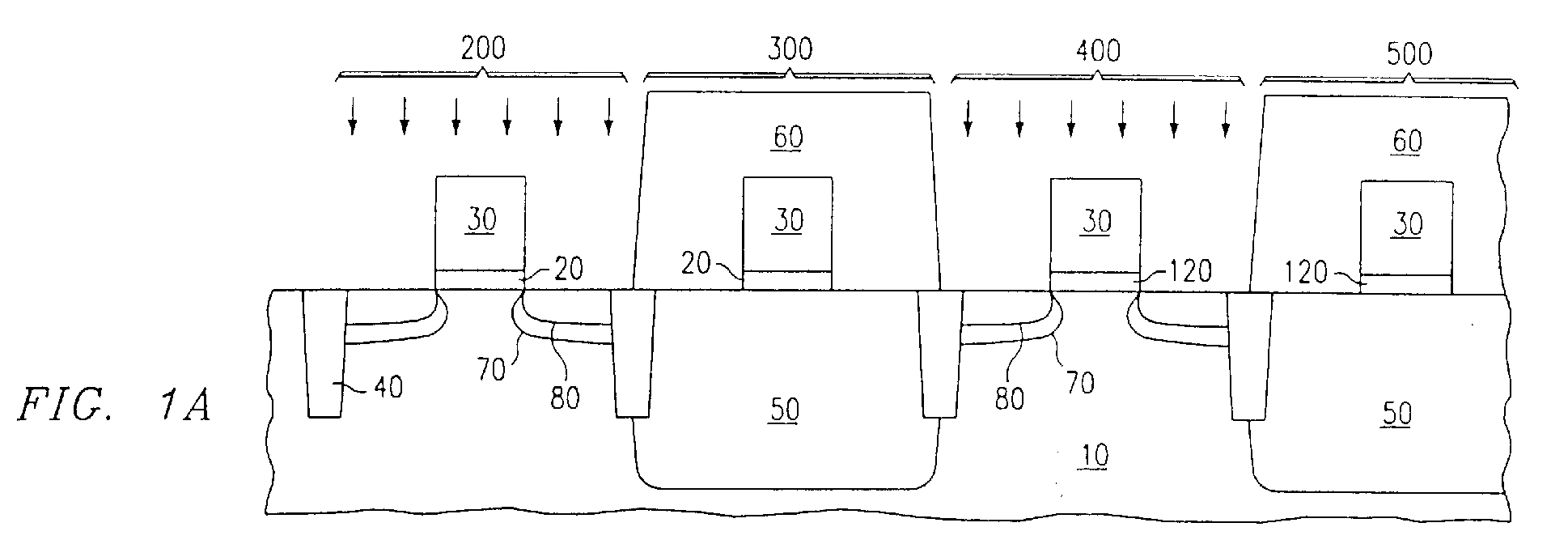
- Contained in the substrate will be isolation structures 40. These isolation structures may comprise an oxide or some other insulator. The purpose of the isolation structure 40 is to isolate the actives devices from one another on the substrate.
- the substrate will contain wells 50 that will be of the opposite conductivity type when compared to the conductivity of the substrate.
- the substrate 10 is p-type and the well 50 is n-type.
- the core NMOS transistor will be fabricated in region 200, the core PMOS transistor in region 300, the I/O NMOS transistor in region 400, and the I/O PMOS transistor in region 500,
- the gate dielectric for the I/O transistors 120 will be thicker than the gate dielectric 20 for the core transistors.
- a layer of photoresist is formed over the substrate 10. Using standard photolithographic techniques, the resist is patterned and etched to produce the areas of resist 60 that cover the PMOS core and I/O transistor.
- a blanket pocket p-type implant followed by a blanket n-type LDD implant is performed resulting in the p-type doping profile 70, and the n-type doping profile 80.
- pocket implants refer to an implant that is used to reduce the effect of the short transistor gate length on transistor properties such as threshold voltage. The effect of the pocket implant is not however limited to threshold voltage.
- the pocket implant for a particular transistor type usually results in a doping profile that extends beyond the drain extension of the transistor.
- the species of the p-type pocket implant can consist of B, BF2, Ga, In, or any other suitable p-type dopant.
- the species of the n-type LDD implant can consist of As, P, Sb, or any other suitable n-type dopant.
- a layer of photoresist is formed on the substrate 10, patterned and etched to form the structure 150 which covers the NMOS core transistor.
- a blanket pocket n-type implant followed by a blanket p-type LDD implant is performed resulting in the n-type doping profile 90, and the p-type doping profile 100.
- the species of the n-type pocket implant can consist of As, P, Sb or any other suitable n-type dopant.
- the species of the p-type LDD implant can consist of B, BF2, Ga, In, or any other suitable p-type dopant.
- the order of the implants is somewhat arbitrary and the LDD implant could be performed before the pocket implant. After completion of the implants the integrated circuit is completed using standard CMOS processing techniques.
Abstract
Description
- The invention is generally related to the field of MOSFET transistors and more specifically to a novel process to achieve high performance core transistor performance and high I/O transistor reliability with reduced mask steps.
- For mixed voltage technologies, e.g. low voltage core transistors with operating voltages of about 1.8 volts to 1.2 V and high voltage input-output (I/O) transistors with operating voltages of about 3.3 volts to 2.5 volts, it is difficult to achieve both high reliability and high performance for both the core transistors and the I/O transistors without adding extra mask steps to independently optimize the core transistors and the I/O transistors.
- The higher operating voltages of the I/O transistors make them susceptible to hot carrier degradation. To reduce this effect, a lightly doped drain (LDD) or drain extension is utilized. In this disclosure, LDD will be used to represent any drain extension type implant. The drain extension typically extend the heavily doped source and drain regions further under the gate of the transistor. In some applications, this LDD is formed using a low dose, high energy arsenic implant which results in acceptable reliability for the high voltage NMOS I/O transistor. In an effort to reduce masking steps, this low dose, high energy arsenic implant can also be used to form the LDD structure in the low voltage core NMOS transistor. However, this LDD structure will significantly degrade the core NMOS transistor drive current (Idrive), most notably, as the drain supply voltage (VDD) for the core is scaled down from about 1.8 volts to about 1.2 volts. This drive current degradation is most probably due to the increase in the series resistance (RsRd) present in the source and drain and the associated LDD structure. As the drain supply voltage is reduced, the drive current will become increasingly limited by the this series resistance.
- Thus the LDD structure required for achieving high reliability in the high voltage NMOS I/O transistors will severely degrade the Idrive in the low voltage NMOS core transistors due to high series resistance RsRd and damage from the high energy arsenic implant. Present integrated circuit fabrication methodologies necessitates the use of additional masking steps to separately optimize both transistors. There is therefore great need for a reduced masking step process that will optimize both transistors and result in both high reliability and high performance without the high cost associated with increased masking steps.
- The instant invention is a mixed voltage CMOS method for high reliability and high performance core and input-output transistors with reduced masks.
- The invention provides a method of fabricating a mixed voltage integrated circuit including the steps of:
- forming a gate dielectric layer on a semiconductor body of a first conductivity type,
- forming a conductive layer on the gate dielectric layer,
- forming a transistor gate stack on the semiconductor body by etching the gate dielectric layer and the conductive layer,
- forming a first doped region of the first conductivity type, below the surface of the semiconductor body adjacent to the transistor gate stack, by implanting a first dopant into the semiconductor body adjacent to the transistor gate stack and
- forming a second doped region of conductivity type opposite to the first conductivity type, between the surface of the semiconductor body and where the first doped region has been or will be implanted, by implanting a second dopant into the semiconductor body adjacent to the transistor gate stack,
- both the first doped region and the second doped region being separated into two parts which are so positioned in relation to the transistor gate stack as to be capable of functioning as transistor source and drain regions.
-
- Additionally, the method may include the steps of:
- forming a third doped region of conductivity type opposite to the first conductivity type, at a depth below the surface of the semiconductor body which places the first doped region between the second and third doped regions, by implanting a third dopant into the semiconductor body adjacent to the transistor gate stack and
- forming a fourth doped region of the first conductivity type, between the surface of the semiconductor body and the second doped region, by implanting a fourth dopant into the semiconductor body adjacent to the transistor gate stack,
- both the third doped region and the fourth doped region being separated into two parts which are so positioned in relation to the transistor gate stack as to be capable of functioning as elements of the transistor source and drain regions.
-
- The method includes the step of forming the semiconductor body as a well in a semiconductor substrate when a PMOS transistor is formed in an n-type substrate.
- Preferably, the method is repeated to form a plurality of transistor gate stacks on the semiconductor body and a plurality of respective first and second doped regions, in the semiconductor body, associated with the transistor gate stacks.
- Preferably, the method includes the steps of:
- forming a third doped region of conductivity type opposite to the first conductivity type, at a depth below the surface of the semiconductor body which places a selected first doped region between the second and third doped regions, by implanting a third dopant into the semiconductor body adjacent to the transistor gate stack with which the selected first doped region is associated and
- forming a fourth doped region of the first conductivity type, between the surface of the semiconductor body and the second doped region with which the selected first doped region is associated, by implanting a fourth dopant into the semiconductor body adjacent to the transistor gate stack respective to the selected first doped region,
- both the third doped region and the fourth doped region being separated into two parts which are so positioned in relation to the transistor gate stack respective to the selected first doped region as to be capable of functioning as elements of the transistor source and drain regions.
-
- The method may be repeated to form a first transistor gate stack on a first semiconductor body of a first conductivity type and a second transistor gate stack on a second semiconductor body of conductivity type opposite the first conductivity type, the second semiconductor body being in the form of a well in the first semiconductor body and the dielectric layer of the second transistor gate stack is thicker than the dielectric layer of the first transistor gate stack.
- Fabricating a mixed voltage integrated circuit may comprise the steps of:
- forming a gate dielectric on a semiconductor substrate;
- forming a conductive layer on said gate dielectric;
- etching said conductive layer and said gate dielectric to form a transistor gate stack;
- implanting said transistor gate stack with a first implant of a first conductivity type;
- implanting said transistor gate stack with a second implant of a second conductivity opposite that of the first conductivity type; and
- implanting said transistor gate stack with a third implant of said first conductivity type.
-
- An embodiment of the instant invention is a method of making a reliable NMOS input-output transistor comprising the steps of: forming at least one region of a second conductivity type in a semiconductor substrate of a first conductivity type; forming a gate dielectric of a first thickness on said semiconductor substrate; forming a gate dielectric of a second thickness on said semiconductor substrate wherein said gate dielectric of a second thickness is equal to or thicker than said gate dielectric of a first thickness; forming a first conductive layer on said gate dielectric of a first thickness; forming a second conductive layer on said gate dielectric of a second thickness; etching said first conductive layer and said gate dielectric of a first thickness to form a first transistor gate stack on said semiconductor substrate of a first conductivity type; etching said first conductive layer and said gate dielectric of a first thickness to form a second transistor gate stack on said semiconductor substrate of a second conductivity type; etching said second conductive layer and said gate dielectric of a second thickness to form a third transistor gate stack on said semiconductor substrate of a first conductivity type; simultaneously implanting said first transistor gate stack and said third transistor gate stack with a first implant of a first species type; simultaneously implanting said first transistor gate stack and said third transistor gate stack with a second implant of a second species type; simultaneously implanting said second transistor gate stack and said third transistor gate stack with a third implant of said first species type; and simultaneously implanting said second transistor gate stack and said third transistor gate stack with a fourth implant of said second species type. Preferably, the first conductivity type is p-type and the second conductivity is n-type. The first implant species type is comprised of a material selected from the group consisting of: B, BF2, Ga, In, and any combination thereof, and the second species type is comprised of a material selected from the group consisting of: As, P, Sb, and any combination thereof.
- Another embodiment of the instant invention is a method of fabricating a mixed voltage integrated circuit, comprising the steps of: forming at least one region of a second conductivity type in a semiconductor substrate of a first conductivity type opposite said second conductivity type; forming a gate dielectric on said semiconductor substrate; forming a conductive layer on said gate dielectric; etching said conductive layer and said gate dielectric to form a first transistor gate stack on said semiconductor substrate and a second transistor gate stack on said one region of said second conductivity type; and simultaneously implanting said first transistor gate stack and said second transistor gate stack with a pocket implant for said first transistor gate stack whereby said pocket implant for said first transistor gate stack functions as LDD implant for said second gate stack.
- No additional masking steps evident in known fabrication methods are required for forming the mixed voltage integrated circuits and no implants additional to those required for forming the core transistors are required. In this invention, when two transistors are fabricated at the same time, an implantation step is capable of providing a pocket implant of one transistor at the time of providing a drain extension of the other transistor.
- These and other advantages will be apparent to those of ordinary skill in the art having reference to the specification in conjunction with the drawings.
- In the drawings:
- FIGURES 1A - 1B are cross-sectional diagrams at various steps in the fabrication of the I/O transistor, and
- FIGURE 2 shows the doping profile obtained from a particular embodiment of the invention.
- FIGURE 3 shows a cross-section of an NMOS transistor and a PMOS transistor fabricated in accordance with the invention.
-
- Common reference numerals are used throughout the figures to represent like or similar features. The figures are not drawn to scale and are merely provided for illustrative purposes.
- While the following description of the instant invention revolves around FIGURES 1 - 3, the instant invention can be utilized in any semiconductor device structure. The methodology of the instant invention provides a solution to obtain a reliable high voltage NMOS I/O transistor simultaneously with a high performance, low voltage NMOS core transistor with no extra mask steps.
- The method of the instant invention will result in the following key features of the core NMOS transistor and the I/O NMOS transistor;
- a) The NMOS core transistor will preferably have shallow drain extensions of sufficiently high dose for low RsRd, and very little dopant grading to support the required minimum gate length (Lg min)
- b) The NMOS I/O transistor will preferably have a drain extension of sufficient doping grading for high NMOS I/O reliability and sufficiently low RsRd for acceptable performance. The above key features are achieved by the instant invention with no additional mask steps.
-
- The following description of the instant invention will be related to Figures 1-2. Referring to Figure 1A and 1B,
substrate 10 is provided and agate dielectric 20 is formed onsubstrate 10. Thesubstrate 10 is preferably p-type in conductivity, but n-type substrates can also be used.Gate dielectric 20 may be comprised of an oxide, thermally grown SiO2, a nitride, an oxynitride, or any combination thereof, and is preferably on the order of 1 to 10 nm thick. A layer of silicon containing material (which will be patterned and etched to form gate structure 30) is formed ongate dielectric 20. Preferably, this silicon-containing material is comprised of polycrystalline silicon("poly" or "polysilicon"), but it may be comprised of epitaxial silicon or any other semiconducting material. Contained in the substrate will beisolation structures 40. These isolation structures may comprise an oxide or some other insulator. The purpose of theisolation structure 40 is to isolate the actives devices from one another on the substrate. The substrate will containwells 50 that will be of the opposite conductivity type when compared to the conductivity of the substrate. - For the embodiment of the instant invention shown in Figures 1A and 1B, the
substrate 10 is p-type and the well 50 is n-type. The core NMOS transistor will be fabricated inregion 200, the core PMOS transistor inregion 300, the I/O NMOS transistor inregion 400, and the I/O PMOS transistor inregion 500, The gate dielectric for the I/O transistors 120 will be thicker than thegate dielectric 20 for the core transistors. With thegate structures 30 defined, a layer of photoresist is formed over thesubstrate 10. Using standard photolithographic techniques, the resist is patterned and etched to produce the areas of resist 60 that cover the PMOS core and I/O transistor. A blanket pocket p-type implant followed by a blanket n-type LDD implant is performed resulting in the p-type doping profile 70, and the n-type doping profile 80. In current integrated circuit technology, pocket implants refer to an implant that is used to reduce the effect of the short transistor gate length on transistor properties such as threshold voltage. The effect of the pocket implant is not however limited to threshold voltage. The pocket implant for a particular transistor type usually results in a doping profile that extends beyond the drain extension of the transistor. The species of the p-type pocket implant can consist of B, BF2, Ga, In, or any other suitable p-type dopant. The species of the n-type LDD implant can consist of As, P, Sb, or any other suitable n-type dopant. The order of the implants is somewhat arbitrary and the LDD implant could be performed before the pocket implant. After the completion of the p-type pocket implant, the n-type LDD implant, and any subsequent processing if required, thephotoresist 60 is removed using standard processing techniques. Following the removal of the photoresist any number of processes may be performed. - Referring to Figure 1B, a layer of photoresist is formed on the
substrate 10, patterned and etched to form thestructure 150 which covers the NMOS core transistor. A blanket pocket n-type implant followed by a blanket p-type LDD implant is performed resulting in the n-type doping profile 90, and the p-type doping profile 100. The species of the n-type pocket implant can consist of As, P, Sb or any other suitable n-type dopant. The species of the p-type LDD implant can consist of B, BF2, Ga, In, or any other suitable p-type dopant. The order of the implants is somewhat arbitrary and the LDD implant could be performed before the pocket implant. After completion of the implants the integrated circuit is completed using standard CMOS processing techniques. - In a specific embodiment of the instant invention, the following implants were carried out on the NMOS I/O transistor:
Implant Condition Species NMOS-LDD 1.2x1015cm-2,15keV As NMOS-pocket 2.4x1013cm-2, 15keV B PMOS-LDD 4x1014cm-2, 10keV BF2 PMOS-pocket 3.2x1013cm-2, 60keV P - The resulting doping profile is shown in Figure 2. The NMOS LDD profile is given by 600, the NMOS pocket profile by 610, the PMOS LDD profile by 620, the PMOS pocket profile by 630, and the resulting NMOS I/O transistor profile by 640. This graded region of n-type doping in the NMOS I/O transistor results in a reliable I/O transistor and high performance core transistors without adding mask steps.
- In addition to implant conditions, the final profile will be a function of the thermal cycles that the transistor undergoes during processing. In determining the implant condition that result in the optimal doping profile, the thermal cycles should be factored into the determination.
- A further embodiment of the instant invention is shown in Figure 3. Here a
NMOS transistor 700 and aPMOS transistor 720 are illustrated. These transistors (700 AND 720) could be either core transistors or I/O transistors. In Figure 3, a blanket pocket p-type implant followed by a blanket n-type LDD implant is performed resulting in the p-type doping profile 70, and the n-type doping profile 80. The species of the p-type pocket implant can consist of B, BF2, Ga, In, or any other suitable p-type dopant. The species of the n-type LDD implant can consist of As, P, Sb, or any other suitable n-type dopant. The order of the implants is somewhat arbitrary and the LDD implant could be performed before the pocket implant. In this embodiment, both transistor types receive both implants. The p-type pocket implant for theNMOS transistor 70 will be used as the LDD implant in the PMOS transistor. The n-type LDD implant in theNMOS transistor 80 will be used as the pocket implant in the PMOS transistor. Following these processes, any number of processing steps may be performed to completely fabricate the devices. While this embodiment has been described with respect to a p-type pocket implant and a n-type LDD implant, the method described is equally applicable to n-type pocket and p-type LDD implants. - While this invention has been described with reference to illustrative embodiments, this description is not intended to be construed in a limiting sense. Various modifications and combinations of the illustrative embodiments, as well as other embodiments of the invention will be apparent to persons skilled in the art upon reference to the description. It is therefore intended that the appended claims encompass any such modifications or embodiments.
Claims (10)
- A method of fabricating a mixed voltage integrated circuit including the steps of:forming a gate dielectric layer on a semiconductor body of a first conductivity type,forming a conductive layer on the gate dielectric layer,forming a transistor gate stack on the semiconductor body by etching the gate dielectric layer and the conductive layer,forming a first doped region of the first conductivity type, below the surface of the semiconductor body adjacent to the transistor gate stack, by implanting a first dopant into the semiconductor body adjacent to the transistor gate stack andforming a second doped region of conductivity type opposite to the first conductivity type, between the surface of the semiconductor body and where the first doped region has been or will be implanted , by implanting a second dopant into the semiconductor body adjacent to the transistor gate stack,both the first doped region and the second doped region being separated into two parts which are so positioned in relation to the transistor gate stack as to be capable of functioning as transistor source and drain regions.
- A method as claimed in claim 1, including the steps of:forming a third doped region of conductivity type opposite to the first conductivity type, at a depth below the surface of the semiconductor body which places the first doped region between the second and third doped regions, by implanting a third dopant into the semiconductor body adjacent to the transistor gate stack andforming a fourth doped region of the first conductivity type, between the surface of the semiconductor body and the second doped region, by implanting a fourth dopant into the semiconductor body adjacent to the transistor gate stack,both the third doped region and the fourth doped region being separated into two parts which are so positioned in relation to the transistor gate stack as to be capable of functioning as elements of the transistor source and drain regions.
- A method as claimed in claim 1 or claim 2, including the step of forming the semiconductor body as a well in a semiconductor substrate.
- A method as claimed in claim 1, repeated to form a plurality of transistor gate stacks on the semiconductor body and a plurality of respective first and second doped regions, in the semiconductor body, associated with the transistor gate stacks.
- A method as claimed in claim 4, including the steps of:forming a third doped region of conductivity type opposite to the first conductivity type, at a depth below the surface of the semiconductor body which places a selected first doped region between the associated second and third doped regions, by implanting a third dopant into the semiconductor body adjacent to the transistor gate stack with which the selected first doped region is associated andforming a fourth doped region of the first conductivity type, between the surface of the semiconductor body and the second doped region associated with the selected first doped region, by implanting a fourth dopant into the semiconductor body adjacent to the transistor gate stack with which the selected first doped region is associated,both the third doped region and the fourth doped region being separated into two parts so positioned in relation to the transistor gate stack with which the selected first doped region is associated as to be capable of functioning as elements of the transistor source and drain regions.
- A method as claimed in claim 1, repeated to form a first transistor gate stack on a first transistor body of a first conductivity type and a second transistor gate stack on a second semiconductor body of a conductivity type opposite the first conductivity type, the second semiconductor body being in the form of a well in the first semiconductor body and the dielectric layer of the second transistor gate stack is thicker than the dielectric layer of the first transistor gate stack.
- A method as claimed in any one of claims 1 to 6, wherein the gate dielectric layer is of a material selected from the group consisting of: silicon dioxide, silicon oxynitride, silicon nitride and any combination thereof.
- A method as claimed in any one of claims 1 to 7, wherein the conductive layer is of a material selected from the group consisting of: doped polysilicon, undoped polysilicon, epitaxial silicon and any combination thereof.
- A method as claimed in any one of claims 1 to 8, wherein the first conductivity type is p-type conductivity and p-type conductivity regions are implanted with a dopant selected from the group consisting of: B, BF2, Ga, In and any combination thereof.
- A method as claimed in any one of claims 1 to 8, wherein the first conductivity type is n-type conductivity and n-type conductivity regions are implanted with a dopant selected from the group consisting of: As, P, Sb and any combination thereof.
Applications Claiming Priority (2)
| Application Number | Priority Date | Filing Date | Title |
|---|---|---|---|
| US11897999P | 1999-02-08 | 1999-02-08 | |
| US118979P | 1999-02-08 |
Publications (3)
| Publication Number | Publication Date |
|---|---|
| EP1026738A2 true EP1026738A2 (en) | 2000-08-09 |
| EP1026738A3 EP1026738A3 (en) | 2004-06-23 |
| EP1026738B1 EP1026738B1 (en) | 2006-06-21 |
Family
ID=22381923
Family Applications (1)
| Application Number | Title | Priority Date | Filing Date |
|---|---|---|---|
| EP00300969A Expired - Lifetime EP1026738B1 (en) | 1999-02-08 | 2000-02-08 | Novel mixed voltage CMOS process for high reliability and high performance core and I/O transistors with reduced mask steps |
Country Status (6)
| Country | Link |
|---|---|
| US (1) | US6258644B1 (en) |
| EP (1) | EP1026738B1 (en) |
| JP (1) | JP2000232167A (en) |
| KR (1) | KR20000071335A (en) |
| DE (1) | DE60028847T2 (en) |
| TW (1) | TW459291B (en) |
Cited By (1)
| Publication number | Priority date | Publication date | Assignee | Title |
|---|---|---|---|---|
| EP3340290A1 (en) * | 2016-12-22 | 2018-06-27 | Semiconductor Manufacturing International Corporation (Shanghai) | Semiconductor device and fabrication method thereof |
Families Citing this family (17)
| Publication number | Priority date | Publication date | Assignee | Title |
|---|---|---|---|---|
| US6166417A (en) * | 1998-06-30 | 2000-12-26 | Intel Corporation | Complementary metal gates and a process for implementation |
| US6878968B1 (en) * | 1999-05-10 | 2005-04-12 | Semiconductor Energy Laboratory Co., Ltd. | Semiconductor device |
| JP2001127171A (en) * | 1999-10-26 | 2001-05-11 | Matsushita Electronics Industry Corp | Semiconductor device and method of manufacturing the same |
| US6479339B2 (en) * | 2000-10-10 | 2002-11-12 | Texas Instruments Incorporated | Use of a thin nitride spacer in a split gate embedded analog process |
| US6541819B2 (en) * | 2001-05-24 | 2003-04-01 | Agere Systems Inc. | Semiconductor device having non-power enhanced and power enhanced metal oxide semiconductor devices and a method of manufacture therefor |
| JP4665141B2 (en) * | 2001-06-29 | 2011-04-06 | 富士通セミコンダクター株式会社 | Semiconductor device and manufacturing method thereof |
| JP5073136B2 (en) * | 2001-08-24 | 2012-11-14 | ルネサスエレクトロニクス株式会社 | Semiconductor device |
| KR100450666B1 (en) * | 2001-09-03 | 2004-10-01 | 삼성전자주식회사 | Method of forming selectively metal silicide layer and semiconductor device having the same |
| US6482703B1 (en) * | 2001-09-28 | 2002-11-19 | Taiwan Semiconductor Manufacturing Company | Method for fabricating an electrostatic discharge device in a dual gate oxide process |
| US7585763B2 (en) | 2005-11-07 | 2009-09-08 | Samsung Electronics Co., Ltd. | Methods of fabricating integrated circuit devices using anti-reflective coating as implant blocking layer |
| US7557022B2 (en) * | 2006-06-13 | 2009-07-07 | Texas Instruments Incorporated | Implantation of carbon and/or fluorine in NMOS fabrication |
| KR100808797B1 (en) * | 2006-08-29 | 2008-03-03 | 동부일렉트로닉스 주식회사 | Method of implanting ion in semiconductor device |
| KR100857453B1 (en) * | 2006-09-29 | 2008-09-08 | 한국전자통신연구원 | Light Sensing Pixel of Image Sensor Structure with Low Operating Voltage |
| US7879639B2 (en) * | 2007-04-13 | 2011-02-01 | Taiwan Semiconductor Manufacturing Company, Ltd. | Method and device to reduce dark current in image sensors |
| FR2939962B1 (en) | 2008-12-15 | 2011-03-18 | Soitec Silicon On Insulator | METHOD OF SLURING A STRUCTURE |
| JP5672055B2 (en) * | 2011-02-23 | 2015-02-18 | 富士通セミコンダクター株式会社 | Manufacturing method of semiconductor device |
| CN111370372B (en) * | 2020-04-22 | 2024-01-19 | 上海华虹宏力半导体制造有限公司 | Manufacturing method of CMOS integrated device |
Citations (3)
| Publication number | Priority date | Publication date | Assignee | Title |
|---|---|---|---|---|
| EP0535917A2 (en) * | 1991-09-30 | 1993-04-07 | STMicroelectronics, Inc. | Method for fabricating integrated circuit transistors |
| US5480828A (en) * | 1994-09-30 | 1996-01-02 | Taiwan Semiconductor Manufacturing Corp. Ltd. | Differential gate oxide process by depressing or enhancing oxidation rate for mixed 3/5 V CMOS process |
| US5580805A (en) * | 1993-09-10 | 1996-12-03 | Sony Corporation | Semiconductor device having various threshold voltages and manufacturing same |
Family Cites Families (4)
| Publication number | Priority date | Publication date | Assignee | Title |
|---|---|---|---|---|
| US5364810A (en) * | 1992-07-28 | 1994-11-15 | Motorola, Inc. | Methods of forming a vertical field-effect transistor and a semiconductor memory cell |
| FR2700418B1 (en) * | 1993-01-12 | 1995-04-07 | France Telecom | Electronic component capable of negative dynamic resistance and corresponding manufacturing process. |
| US5780897A (en) * | 1995-11-13 | 1998-07-14 | Digital Equipment Corporation | ESD protection clamp for mixed voltage I/O stages using NMOS transistors |
| US6075271A (en) * | 1998-03-03 | 2000-06-13 | Motorola, Inc. | Semiconductor device inhibiting parasitic effects during electrostatic discharge |
-
2000
- 2000-02-08 EP EP00300969A patent/EP1026738B1/en not_active Expired - Lifetime
- 2000-02-08 KR KR1020000005722A patent/KR20000071335A/en not_active Application Discontinuation
- 2000-02-08 US US09/499,719 patent/US6258644B1/en not_active Expired - Lifetime
- 2000-02-08 JP JP2000030167A patent/JP2000232167A/en not_active Abandoned
- 2000-02-08 DE DE60028847T patent/DE60028847T2/en not_active Expired - Lifetime
- 2000-03-09 TW TW089101872A patent/TW459291B/en not_active IP Right Cessation
Patent Citations (3)
| Publication number | Priority date | Publication date | Assignee | Title |
|---|---|---|---|---|
| EP0535917A2 (en) * | 1991-09-30 | 1993-04-07 | STMicroelectronics, Inc. | Method for fabricating integrated circuit transistors |
| US5580805A (en) * | 1993-09-10 | 1996-12-03 | Sony Corporation | Semiconductor device having various threshold voltages and manufacturing same |
| US5480828A (en) * | 1994-09-30 | 1996-01-02 | Taiwan Semiconductor Manufacturing Corp. Ltd. | Differential gate oxide process by depressing or enhancing oxidation rate for mixed 3/5 V CMOS process |
Cited By (5)
| Publication number | Priority date | Publication date | Assignee | Title |
|---|---|---|---|---|
| EP3340290A1 (en) * | 2016-12-22 | 2018-06-27 | Semiconductor Manufacturing International Corporation (Shanghai) | Semiconductor device and fabrication method thereof |
| US20180182626A1 (en) * | 2016-12-22 | 2018-06-28 | Semiconductor Manufacturing International (Shanghai) Corporation | Semiconductor device and fabrication method thereof |
| CN108231682A (en) * | 2016-12-22 | 2018-06-29 | 中芯国际集成电路制造(上海)有限公司 | Semiconductor devices and forming method thereof |
| US10727130B2 (en) * | 2016-12-22 | 2020-07-28 | Semiconductor Manufacturing International (Shanghai) Corporation | Semiconductor device and fabrication method thereof |
| CN108231682B (en) * | 2016-12-22 | 2021-02-02 | 中芯国际集成电路制造(上海)有限公司 | Semiconductor device and method of forming the same |
Also Published As
| Publication number | Publication date |
|---|---|
| EP1026738B1 (en) | 2006-06-21 |
| US6258644B1 (en) | 2001-07-10 |
| DE60028847D1 (en) | 2006-08-03 |
| JP2000232167A (en) | 2000-08-22 |
| KR20000071335A (en) | 2000-11-25 |
| EP1026738A3 (en) | 2004-06-23 |
| DE60028847T2 (en) | 2006-12-07 |
| TW459291B (en) | 2001-10-11 |
Similar Documents
| Publication | Publication Date | Title |
|---|---|---|
| US6548874B1 (en) | Higher voltage transistors for sub micron CMOS processes | |
| US6514810B1 (en) | Buried channel PMOS transistor in dual gate CMOS with reduced masking steps | |
| US6153455A (en) | Method of fabricating ultra shallow junction CMOS transistors with nitride disposable spacer | |
| US6316302B1 (en) | Isotropically etching sidewall spacers to be used for both an NMOS source/drain implant and a PMOS LDD implant | |
| US4435895A (en) | Process for forming complementary integrated circuit devices | |
| US5427964A (en) | Insulated gate field effect transistor and method for fabricating | |
| EP1026738B1 (en) | Novel mixed voltage CMOS process for high reliability and high performance core and I/O transistors with reduced mask steps | |
| US6660603B2 (en) | Higher voltage drain extended MOS transistors with self-aligned channel and drain extensions | |
| JP2002033396A (en) | Manufacturing method of i/o and core device compatible with high characteristic and reliability i/o device and analog using core and device impregnation | |
| WO1998008253A1 (en) | Dual gate oxide thickness integrated circuit and process for making same | |
| US6479339B2 (en) | Use of a thin nitride spacer in a split gate embedded analog process | |
| KR100823821B1 (en) | A method of making semiconductor integrated circuit | |
| EP0676798A2 (en) | Insulated gate field effect transistor with assymetric channel and method for fabricating | |
| US20030127694A1 (en) | Higher voltage transistors for sub micron CMOS processes | |
| US6908800B1 (en) | Tunable sidewall spacer process for CMOS integrated circuits | |
| US6583013B1 (en) | Method for forming a mixed voltage circuit having complementary devices | |
| US6303420B1 (en) | Integrated bipolar junction transistor for mixed signal circuits | |
| CN108231767B (en) | Device structure with multiple nitride layers | |
| JP4501183B2 (en) | Manufacturing method of semiconductor device | |
| KR100632068B1 (en) | Method for manufacturing mos transistor of semiconductor device | |
| US7553718B2 (en) | Methods, systems and structures for forming semiconductor structures incorporating high-temperature processing steps | |
| US6743679B2 (en) | Integrated circuit devices with high and low voltage components and processes for manufacturing these devices | |
| US5804497A (en) | Selectively doped channel region for increased IDsat and method for making same | |
| US7560779B2 (en) | Method for forming a mixed voltage circuit having complementary devices | |
| US7635618B2 (en) | Integrated circuit devices with high and low voltage components and processes for manufacturing these devices |
Legal Events
| Date | Code | Title | Description |
|---|---|---|---|
| PUAI | Public reference made under article 153(3) epc to a published international application that has entered the european phase |
Free format text: ORIGINAL CODE: 0009012 |
|
| AK | Designated contracting states |
Kind code of ref document: A2 Designated state(s): AT BE CH CY DE DK ES FI FR GB GR IE IT LI LU MC NL PT SE |
|
| AX | Request for extension of the european patent |
Free format text: AL;LT;LV;MK;RO;SI |
|
| RIN1 | Information on inventor provided before grant (corrected) |
Inventor name: MEHROTRA, MANOJ Inventor name: NANDAKUMAR, MAHALINGAM Inventor name: RODDER, MARK S. |
|
| PUAL | Search report despatched |
Free format text: ORIGINAL CODE: 0009013 |
|
| AK | Designated contracting states |
Kind code of ref document: A3 Designated state(s): AT BE CH CY DE DK ES FI FR GB GR IE IT LI LU MC NL PT SE |
|
| AX | Request for extension of the european patent |
Extension state: AL LT LV MK RO SI |
|
| 17P | Request for examination filed |
Effective date: 20041209 |
|
| AKX | Designation fees paid |
Designated state(s): DE FR GB |
|
| 17Q | First examination report despatched |
Effective date: 20050309 |
|
| GRAP | Despatch of communication of intention to grant a patent |
Free format text: ORIGINAL CODE: EPIDOSNIGR1 |
|
| RIN1 | Information on inventor provided before grant (corrected) |
Inventor name: NANDAKUMAR, MAHALINGAM Inventor name: MEHROTRA, MANOJ Inventor name: RODDER, MARK S. |
|
| GRAS | Grant fee paid |
Free format text: ORIGINAL CODE: EPIDOSNIGR3 |
|
| GRAA | (expected) grant |
Free format text: ORIGINAL CODE: 0009210 |
|
| AK | Designated contracting states |
Kind code of ref document: B1 Designated state(s): DE FR GB |
|
| REG | Reference to a national code |
Ref country code: GB Ref legal event code: FG4D |
|
| RIN1 | Information on inventor provided before grant (corrected) |
Inventor name: NANDAKUMAR, MAHALINGAM Inventor name: RODDER, MARK S. Inventor name: MEHROTRA, MANOJ |
|
| REF | Corresponds to: |
Ref document number: 60028847 Country of ref document: DE Date of ref document: 20060803 Kind code of ref document: P |
|
| PLBE | No opposition filed within time limit |
Free format text: ORIGINAL CODE: 0009261 |
|
| STAA | Information on the status of an ep patent application or granted ep patent |
Free format text: STATUS: NO OPPOSITION FILED WITHIN TIME LIMIT |
|
| EN | Fr: translation not filed | ||
| 26N | No opposition filed |
Effective date: 20070322 |
|
| PG25 | Lapsed in a contracting state [announced via postgrant information from national office to epo] |
Ref country code: FR Free format text: LAPSE BECAUSE OF FAILURE TO SUBMIT A TRANSLATION OF THE DESCRIPTION OR TO PAY THE FEE WITHIN THE PRESCRIBED TIME-LIMIT Effective date: 20070309 |
|
| PG25 | Lapsed in a contracting state [announced via postgrant information from national office to epo] |
Ref country code: FR Free format text: LAPSE BECAUSE OF FAILURE TO SUBMIT A TRANSLATION OF THE DESCRIPTION OR TO PAY THE FEE WITHIN THE PRESCRIBED TIME-LIMIT Effective date: 20060621 |
|
| PGFP | Annual fee paid to national office [announced via postgrant information from national office to epo] |
Ref country code: DE Payment date: 20150227 Year of fee payment: 16 |
|
| PGFP | Annual fee paid to national office [announced via postgrant information from national office to epo] |
Ref country code: GB Payment date: 20150126 Year of fee payment: 16 |
|
| REG | Reference to a national code |
Ref country code: DE Ref legal event code: R119 Ref document number: 60028847 Country of ref document: DE |
|
| GBPC | Gb: european patent ceased through non-payment of renewal fee |
Effective date: 20160208 |
|
| PG25 | Lapsed in a contracting state [announced via postgrant information from national office to epo] |
Ref country code: DE Free format text: LAPSE BECAUSE OF NON-PAYMENT OF DUE FEES Effective date: 20160901 Ref country code: GB Free format text: LAPSE BECAUSE OF NON-PAYMENT OF DUE FEES Effective date: 20160208 |