EP1032099A2 - Semiconductor device and method of fabricating the same - Google Patents
Semiconductor device and method of fabricating the same Download PDFInfo
- Publication number
- EP1032099A2 EP1032099A2 EP00103996A EP00103996A EP1032099A2 EP 1032099 A2 EP1032099 A2 EP 1032099A2 EP 00103996 A EP00103996 A EP 00103996A EP 00103996 A EP00103996 A EP 00103996A EP 1032099 A2 EP1032099 A2 EP 1032099A2
- Authority
- EP
- European Patent Office
- Prior art keywords
- thermal expansion
- expansion coefficient
- layer
- substrate
- strain reducing
- Prior art date
- Legal status (The legal status is an assumption and is not a legal conclusion. Google has not performed a legal analysis and makes no representation as to the accuracy of the status listed.)
- Withdrawn
Links
Images


Classifications
-
- H—ELECTRICITY
- H01—ELECTRIC ELEMENTS
- H01L—SEMICONDUCTOR DEVICES NOT COVERED BY CLASS H10
- H01L33/00—Semiconductor devices with at least one potential-jump barrier or surface barrier specially adapted for light emission; Processes or apparatus specially adapted for the manufacture or treatment thereof or of parts thereof; Details thereof
- H01L33/005—Processes
- H01L33/0062—Processes for devices with an active region comprising only III-V compounds
- H01L33/0066—Processes for devices with an active region comprising only III-V compounds with a substrate not being a III-V compound
- H01L33/007—Processes for devices with an active region comprising only III-V compounds with a substrate not being a III-V compound comprising nitride compounds
-
- H—ELECTRICITY
- H01—ELECTRIC ELEMENTS
- H01L—SEMICONDUCTOR DEVICES NOT COVERED BY CLASS H10
- H01L21/00—Processes or apparatus adapted for the manufacture or treatment of semiconductor or solid state devices or of parts thereof
- H01L21/02—Manufacture or treatment of semiconductor devices or of parts thereof
- H01L21/02104—Forming layers
- H01L21/02365—Forming inorganic semiconducting materials on a substrate
- H01L21/02367—Substrates
- H01L21/0237—Materials
- H01L21/02373—Group 14 semiconducting materials
- H01L21/02381—Silicon, silicon germanium, germanium
-
- H—ELECTRICITY
- H01—ELECTRIC ELEMENTS
- H01L—SEMICONDUCTOR DEVICES NOT COVERED BY CLASS H10
- H01L21/00—Processes or apparatus adapted for the manufacture or treatment of semiconductor or solid state devices or of parts thereof
- H01L21/02—Manufacture or treatment of semiconductor devices or of parts thereof
- H01L21/02104—Forming layers
- H01L21/02365—Forming inorganic semiconducting materials on a substrate
- H01L21/02367—Substrates
- H01L21/0237—Materials
- H01L21/0242—Crystalline insulating materials
-
- H—ELECTRICITY
- H01—ELECTRIC ELEMENTS
- H01L—SEMICONDUCTOR DEVICES NOT COVERED BY CLASS H10
- H01L21/00—Processes or apparatus adapted for the manufacture or treatment of semiconductor or solid state devices or of parts thereof
- H01L21/02—Manufacture or treatment of semiconductor devices or of parts thereof
- H01L21/02104—Forming layers
- H01L21/02365—Forming inorganic semiconducting materials on a substrate
- H01L21/02436—Intermediate layers between substrates and deposited layers
- H01L21/02439—Materials
- H01L21/02441—Group 14 semiconducting materials
- H01L21/0245—Silicon, silicon germanium, germanium
-
- H—ELECTRICITY
- H01—ELECTRIC ELEMENTS
- H01L—SEMICONDUCTOR DEVICES NOT COVERED BY CLASS H10
- H01L21/00—Processes or apparatus adapted for the manufacture or treatment of semiconductor or solid state devices or of parts thereof
- H01L21/02—Manufacture or treatment of semiconductor devices or of parts thereof
- H01L21/02104—Forming layers
- H01L21/02365—Forming inorganic semiconducting materials on a substrate
- H01L21/02436—Intermediate layers between substrates and deposited layers
- H01L21/02439—Materials
- H01L21/02455—Group 13/15 materials
- H01L21/02458—Nitrides
-
- H—ELECTRICITY
- H01—ELECTRIC ELEMENTS
- H01L—SEMICONDUCTOR DEVICES NOT COVERED BY CLASS H10
- H01L21/00—Processes or apparatus adapted for the manufacture or treatment of semiconductor or solid state devices or of parts thereof
- H01L21/02—Manufacture or treatment of semiconductor devices or of parts thereof
- H01L21/02104—Forming layers
- H01L21/02365—Forming inorganic semiconducting materials on a substrate
- H01L21/02436—Intermediate layers between substrates and deposited layers
- H01L21/02494—Structure
- H01L21/02496—Layer structure
- H01L21/02502—Layer structure consisting of two layers
-
- H—ELECTRICITY
- H01—ELECTRIC ELEMENTS
- H01L—SEMICONDUCTOR DEVICES NOT COVERED BY CLASS H10
- H01L21/00—Processes or apparatus adapted for the manufacture or treatment of semiconductor or solid state devices or of parts thereof
- H01L21/02—Manufacture or treatment of semiconductor devices or of parts thereof
- H01L21/02104—Forming layers
- H01L21/02365—Forming inorganic semiconducting materials on a substrate
- H01L21/02518—Deposited layers
- H01L21/02521—Materials
- H01L21/02538—Group 13/15 materials
- H01L21/0254—Nitrides
-
- H—ELECTRICITY
- H01—ELECTRIC ELEMENTS
- H01L—SEMICONDUCTOR DEVICES NOT COVERED BY CLASS H10
- H01L33/00—Semiconductor devices with at least one potential-jump barrier or surface barrier specially adapted for light emission; Processes or apparatus specially adapted for the manufacture or treatment thereof or of parts thereof; Details thereof
- H01L33/005—Processes
- H01L33/0093—Wafer bonding; Removal of the growth substrate
-
- H—ELECTRICITY
- H01—ELECTRIC ELEMENTS
- H01S—DEVICES USING THE PROCESS OF LIGHT AMPLIFICATION BY STIMULATED EMISSION OF RADIATION [LASER] TO AMPLIFY OR GENERATE LIGHT; DEVICES USING STIMULATED EMISSION OF ELECTROMAGNETIC RADIATION IN WAVE RANGES OTHER THAN OPTICAL
- H01S5/00—Semiconductor lasers
- H01S5/30—Structure or shape of the active region; Materials used for the active region
- H01S5/32—Structure or shape of the active region; Materials used for the active region comprising PN junctions, e.g. hetero- or double- heterostructures
- H01S5/323—Structure or shape of the active region; Materials used for the active region comprising PN junctions, e.g. hetero- or double- heterostructures in AIIIBV compounds, e.g. AlGaAs-laser, InP-based laser
- H01S5/32308—Structure or shape of the active region; Materials used for the active region comprising PN junctions, e.g. hetero- or double- heterostructures in AIIIBV compounds, e.g. AlGaAs-laser, InP-based laser emitting light at a wavelength less than 900 nm
- H01S5/32341—Structure or shape of the active region; Materials used for the active region comprising PN junctions, e.g. hetero- or double- heterostructures in AIIIBV compounds, e.g. AlGaAs-laser, InP-based laser emitting light at a wavelength less than 900 nm blue laser based on GaN or GaP
Definitions
- the present invention relates to a semiconductor device comprising a nitride compound semiconductor layer and a method of fabricating the same.
- a nitride compound semiconductor such as GaN, InN, or AlN is a material suitable for use in a blue semiconductor laser device or in a transistor operable at a high speed even at a high temperature.
- a laser diode comprising a nitride compound semiconductor layer formed on a silicon substrate will be described with reference to Figure 6 .
- an AlN layer 11 as a buffer layer, a GaN layer 12 as a first contact layer, a first clad layer 13 made of n-type AlGaN, an active layer 14 made of undoped GaInN, a second clad layer 15 made of p-type AlGaN, and a second contact layer 16 made of p-type GaN are stacked successively in layers on a silicon substrate 10 .
- the AlN layer 11 is formed by growing an AlN crystal on the silicon substrate 10 .
- the GaN layer 12 is formed by growing a GaN crystal on the AlN layer 11 at a temperature of 1050 °C and doped with an impurity such as Si, Ge, or Se to have the n-type conductivity.
- MOVPE metal organic vapor phase epitaxial growth
- a tensile strain is applied from the silicon substrate 10 to the GaN layer 12 and an internal stress is produced in the GaN layer 12 in response to the tensile strain when the temperature of the silicon substrate 10 is lowered from the crystal growth temperature of 1050 °C to a room temperature after the formation of the GaN layer 12 .
- the internal stress produced in the GaN layer 12 increases disadvantageously to form a crack (crevice) in the GaN layer 12 .
- the method for the crystal growth of a nitride compound semiconductor on a silicon substrate is not practical.
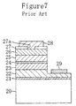
- a laser diode comprising a nitride compound semiconductor layer formed on a sapphire substrate will be described with reference to Figure 7 .
- an AlN layer 21 as a buffer layer, a GaN layer 22 as a first contact layer, a first clad layer 23 made of n-type AlGaN, an active layer 24 made of undoped GaInN, a second clad layer 25 made of p-type AlGaN, and a second contact layer 26 made of p-type GaN are stacked successively in layers on a sapphire substrate 20 .
- the AlN layer 21 is formed by growing an AlN crystal on the sapphire substrate 20 .
- the GaN layer 22 is formed by growing a GaN crystal on the AlN layer 21 by using MOVPE at a temperature of 1050 °C.
- the GaN layer 22 is doped with an impurity such as Si, Ge, or Se to have the n-type conductivity. It is to be noted that a device structure composed of the GaN layer 22 as the first contact layer, the first clad layer 23 , the active layer 24 , the second clad layer 25 , and the second contact layer 26 has been partially removed by dry etching till the GaN layer 22 is etched halfway.
- a p-type electrode 28 made of an Ni-Au alloy is formed on the second contact layer 26 with a current restricting layer 27 having an opening 27a interposed therebetween, while an n-type electrode 29 made of an Ni-Au alloy is formed in a space corresponding to the etched portion of the GaN layer 22 , i.e., the first contact layer.
- a crack is less likely to occur in the GaN layer 22 than in the first conventional embodiment since the difference between the thermal expansion coefficient (7.5 x 10 -6 /K) of sapphire (Al 2 O 3 ) and the thermal expansion coefficient of GaN is smaller than the difference between the thermal expansion coefficient of Si and that of GaN.
- a compression strain is applied from the sapphire substrate 20 to the GaN layer 22 and an internal stress is produced in the GaN layer 22 in response to the compression strain when the temperature of the sapphire substrate 20 is lowered from the crystal growth temperature of 1050 °C to a room temperature after the formation of the GaN layer 22, since the thermal expansion coefficient of sapphire is higher than that of GaN.
- the second conventional embodiment also presents the second problem that it is difficult to fabricate a laser diode having a smooth reflecting mirror surface since it is difficult to cleave the sapphire substrate 20 .
- an AlN layer 31 as a buffer layer is formed by growing an AlN crystal on a sapphire substrate 30 .
- a GaN layer 32 as a compound semiconductor layer is formed by growing a GaN crystal on the AlN layer 31 at a temperature of 1050 °C.
- the AlN layer 31 and the GaN layer 32 are separated from the sapphire substrate 30 by removing the sapphire substrate 30 by polishing, whereby a semiconductor substrate 33 composed of the AlN layer 31 and the GaN layer 32 is formed.
- a first contact layer 34 made of n-type GaN, a first clad layer 35 made of n-type AlGaN, an active layer 36 made of undoped GaInN, a second clad layer 37 made of p-type AlGaN, and a second contact layer 38 made of p-type GaN are formed successively on the semiconductor substrate 33 .
- a p-type electrode is formed on the second contact layer 38 with a current restricting layer interposed therebetween and an n-type electrode is formed on a back surface of the semiconductor substrate 33 , though they are not depicted, whereby the laser diode is completed.
- a laser diode having a smooth reflecting mirror surface can be fabricated since the semiconductor substrate 33 is cleaved easily.
- the third conventional embodiment has the problem that the crystalline characteristics of the GaN layer 32 composing the semiconductor substrate 33 cannot be improved due to the difference between the thermal expansion coefficient of sapphire and that of GaN, similarly to the second conventional embodiment.
- the third conventional embodiment also has the problem that the crystalline characteristics of the GaN layer are further degraded as the thickness of the GaN layer 32 , i.e., the thickness of the semiconductor substrate 33 is increased.
- a first semiconductor device comprises: a substrate having a first thermal expansion coefficient T1; a strain reducing layer having a second thermal expansion coefficient T2, the strain reducing layer being formed on the substrate; and a semiconductor layer having a third thermal expansion coefficient T3, the semiconductor layer being formed on the strain reducing layer and made of a nitride compound represented by Al y Ga 1-y-z In z N (0 ⁇ y ⁇ 1, 0 ⁇ z ⁇ 1), the second thermal expansion coefficient T2 being lower than the first thermal expansion coefficient T1, the third thermal expansion coefficient T3 being lower than the first thermal expansion coefficient T1 and higher than the second thermal expansion coefficient T2.
- the strain reducing layer having the second thermal expansion coefficient T2 lower than the first thermal expansion coefficient T1 is formed on the substrate having the first thermal expansion coefficient T1 and the nitride compound semiconductor layer having the third thermal expansion coefficient T3 lower than the first thermal expansion coefficient T1 and higher than the second thermal expansion coefficient T2 is formed on the strain reducing layer. Accordingly, when the temperature of the substrate is lowered from a temperature for the crystal growth of the nitride compound semiconductor layer to a room temperature after the formation of the nitride compound semiconductor layer, a compression strain applied from the substrate to the strain reducing layer and a tensile strain applied from the strain reducing layer to the nitride compound semiconductor layer cancel out each other.
- the nitride compound semiconductor layer having the third thermal expansion coefficient T3 is formed on a multilayer structure composed of the substrate having the first thermal expansion coefficient T1 higher than the third thermal expansion coefficient T3 and the strain reducing layer having the second thermal expansion coefficient T2 lower than the third thermal expansion coefficient T3, the difference between a mean value of the thermal expansion coefficients of the multilayer structure and the third thermal expansion coefficient T3 can be made smaller than the difference between the first and third thermal expansion coefficients T1 and T3.
- an internal stress produced in the nitride compound semiconductor layer in response to the compression strain from the substrate is reduced and cracks are less likely to be formed in the nitride semiconductor layer, so that the crystalline characteristics of the nitride compound semiconductor layer are improved.
- a ratio T1/T3 of the first thermal expansion coefficient T1 to the third thermal expansion coefficient T3 is preferably lower than a ratio T3/T2 of the third thermal expansion coefficient T3 to the second thermal expansion coefficient T2 and the substrate is preferably larger in thickness than the strain reducing layer.
- the arrangement further reduces the difference between the mean value of the thermal expansion coefficients of the multilayer structure composed of the substrate and the strain reducing layer and the third thermal expansion coefficient T3, so that the crystalline characteristics of the nitride compound semiconductor layer are further improved.
- a ratio T1/T3 of the first thermal expansion coefficient T1 to the third thermal expansion coefficient T3 is preferably higher than a ratio T3/T2 of the third thermal expansion coefficient T3 to the second thermal expansion coefficient T2 and the substrate is preferably smaller in thickness than the strain reducing layer.
- the arrangement further reduces the difference between the mean value of the thermal expansion coefficients of the multilayer structure composed of the substrate and the strain reducing layer and the third thermal expansion coefficient T3, so that the crystalline characteristics of the nitride compound semiconductor layer are further improved.
- the substrate is preferably made of sapphire and the strain reducing layer is preferably made of silicon.
- the strain reducing layer having a specified growth interface is formed on the substrate, so that the crystalline characteristics of the nitride compound semiconductor layer formed on the strain reducing layer are further improved.
- the substrate preferably has a main surface having a (0001) plane and the strain reducing layer preferably has a growth interface having a (111) plane.
- the nitride compound semiconductor layer having a growth interface having a (0001) plane is formed on the strain reducing layer formed to have a growth interface having a (111) plane, so that the crystalline characteristics of the nitride compound semiconductor layer are further improved.
- a second semiconductor device comprises: a substrate having a first thermal expansion coefficient T1; a strain reducing layer having a second thermal expansion coefficient T2, the strain reducing layer being formed on the substrate; and a semiconductor layer having a third thermal expansion coefficient T3, the semiconductor layer being formed on the strain reducing layer and made of a nitride compound represented by Al y Ga 1-y-z In z N (0 ⁇ y ⁇ 1, 0 ⁇ z ⁇ 1), the second thermal expansion coefficient T2 being higher than the first thermal expansion coefficient T1, the third thermal expansion coefficient T3 being higher than the first thermal expansion coefficient T1 and lower than the second thermal expansion coefficient T2.
- the strain reducing layer having the second thermal expansion coefficient T2 higher than the first thermal expansion coefficient T1 is formed on the substrate having the first thermal expansion coefficient T1 and the nitride compound semiconductor layer having the third thermal expansion coefficient T3 higher than the first thermal expansion coefficient T1 and lower than the second thermal expansion coefficient T2 is formed on the strain reducing layer. Accordingly, when the temperature of the substrate is lowered from a temperature for the crystal growth of the nitride compound semiconductor layer to a room temperature after the formation of the nitride compound semiconductor layer, a tensile strain applied from the substrate to the strain reducing layer and a compression strain applied from the strain reducing layer to the nitride compound semiconductor layer cancel out each other.
- the nitride compound semiconductor layer having the third thermal expansion coefficient T3 is formed on a multilayer structure composed of the substrate having the first thermal expansion coefficient T1 lower than the third thermal expansion coefficient T3 and the strain reducing layer having the second thermal expansion coefficient T2 higher than the third thermal expansion coefficient T3, the difference between a mean value of the thermal expansion coefficients of the multilayer structure and the third thermal expansion coefficient T3 can be made smaller than the difference between the first and third thermal expansion coefficients T1 and T3.
- an internal stress produced in the nitride compound semiconductor layer in response to the tensile stress from the substrate is reduced and cracks are less likely to be formed in the nitride semiconductor layer, so that the crystalline characteristics of the nitride compound semiconductor layer are improved.
- a ratio T3/T1 of the third thermal expansion coefficient T3 to the first thermal expansion coefficient T1 is preferably lower than a ratio T2/T3 of the second thermal expansion coefficient T2 to the third thermal expansion coefficient T3 and the substrate is preferably larger in thickness than the strain reducing layer.
- the arrangement further reduces the difference between the mean value of the thermal expansion coefficients of the multilayer structure composed of the substrate and the strain reducing layer and the third thermal expansion coefficient T3, so that the crystalline characteristics of the nitride compound semiconductor layer are further improved.
- a ratio T3/T1 of the third thermal expansion coefficient T3 to the first thermal expansion coefficient T1 is preferably higher than a ratio T2/T3 of the second thermal expansion coefficient T2 to the third thermal expansion coefficient T3 and the substrate is preferably smaller in thickness than the strain reducing layer.
- the arrangement further reduces the difference between the mean value of the thermal expansion coefficients of the multilayer structure composed of the substrate and the strain reducing layer and the third thermal expansion coefficient T3, so that the crystalline characteristics of the nitride compound semiconductor layer are further improved.
- a first method of fabricating a semiconductor device comprises the steps of: forming a strain reducing layer having a second thermal expansion coefficient T2 on a substrate having a first thermal expansion coefficient T1; and forming a semiconductor layer having a third thermal expansion coefficient T3 on the strain reducing layer, the semiconductor layer being made of a nitride compound represented by Al y Ga 1-y-z In z N (0 ⁇ y ⁇ 1, 0 ⁇ z ⁇ 1), the second thermal expansion coefficient T2 being lower than the first thermal expansion coefficient T1, the third thermal expansion coefficient T3 being lower than the first thermal expansion coefficient T1 and higher than the second thermal expansion coefficient T2.
- the strain reducing layer having the second thermal expansion coefficient T2 lower than the first thermal expansion coefficient T1 is formed on the substrate having the first thermal expansion coefficient T1 and then the nitride compound semiconductor layer having the third thermal expansion coefficient T3 lower than the first thermal expansion coefficient T1 and higher than the second thermal expansion coefficient T2 is formed on the strain reducing layer. Accordingly, when the temperature of the substrate is lowered from a temperature for the crystal growth of the nitride compound semiconductor layer to a room temperature after the formation of the nitride compound semiconductor layer, a compression strain applied from the substrate to the strain reducing layer and a tensile strain applied from the strain reducing layer to the nitride compound semiconductor layer cancel out each other.
- the nitride compound semiconductor layer having the third thermal expansion coefficient T3 is formed on a multilayer structure composed of the substrate having the first thermal expansion coefficient T1 higher than the third thermal expansion coefficient T3 and the strain reducing layer having the second thermal expansion coefficient T2 lower than the third thermal expansion coefficient T3, the difference between a mean value of the thermal expansion coefficients of the multilayer structure and the third thermal expansion coefficient T3 can be made smaller than the difference between the first and third thermal expansion coefficients T1 and T3.
- an internal stress produced in the nitride compound semiconductor layer in response to the compression strain from the substrate is reduced and cracks are less likely to be formed in the nitride semiconductor layer, so that the crystalline characteristics of the nitride compound semiconductor layer are improved.
- the step of forming the strain reducing layer preferably includes the step of forming, when a ratio T1/T3 of the first thermal expansion coefficient T1 to the third thermal expansion coefficient T3 is lower than a ratio T3/T2 of the third thermal expansion coefficient T3 to the second thermal expansion coefficient T2, the strain reducing layer such that the strain reducing layer is smaller in thickness than the substrate and forming, when the ratio T1/T3 of the first thermal expansion coefficient T1 to the third thermal expansion coefficient T3 is higher than the ratio T3/T2 of the third thermal expansion coefficient T3 to the second thermal expansion coefficient T2, the strain reducing layer such that the strain reducing layer is larger in thickness than the substrate.
- the arrangement further reduces the difference between the mean value of the thermal expansion coefficients of the multilayer structure composed of the substrate and the strain reducing layer and the third thermal expansion coefficient T3, so that the crystalline characteristics of the nitride compound semiconductor layer are further improved.
- the substrate is preferably made of sapphire and the strain reducing layer is preferably made of silicon.
- the strain reducing layer having a specified growth interface is formed on the substrate, so that the crystalline characteristics of the nitride compound semiconductor layer formed on the strain reducing layer are further improved.
- the step of forming the strain reducing layer preferably includes the step of forming the strain reducing layer having a growth interface having a (111) plane on the substrate having a main surface having a (0001) plane.
- the nitride compound semiconductor layer having a growth interface having a (0001) plane is formed on the strain reducing layer formed to have a growth interface having a (111) plane, so that the crystalline characteristics of the nitride compound semiconductor layer are further improved.
- a second method of fabricating a semiconductor device comprises the steps of: forming a strain reducing layer having a second thermal expansion coefficient T2 on a substrate having a first thermal expansion coefficient T1; and forming a semiconductor layer having a third thermal expansion coefficient T3 on the strain reducing layer, the semiconductor layer being made of a nitride compound represented by Al y Ga 1-y-z In z N (0 ⁇ y ⁇ 1, 0 ⁇ z ⁇ 1), the second thermal expansion coefficient T2 being higher than the first thermal expansion coefficient T1, the third thermal expansion coefficient T3 being higher than the first thermal expansion coefficient T1 and lower than the second thermal expansion coefficient T2.
- the strain reducing layer having the second thermal expansion coefficient T2 higher than the first thermal expansion coefficient T1 is formed on the substrate having the first thermal expansion coefficient T1 and then the nitride compound semiconductor layer having the third thermal expansion coefficient T3 higher than the first thermal expansion coefficient T1 and lower than the second thermal expansion coefficient T2 is formed on the strain reducing layer. Accordingly, when the temperature of the substrate is lowered from a temperature for the crystal growth of the nitride compound semiconductor layer to a room temperature after the formation of the nitride compound semiconductor layer, a tensile strain applied from the substrate to the strain reducing layer and a compression strain applied from the strain reducing layer to the nitride compound semiconductor layer cancel out each other.
- the nitride compound semiconductor layer having the third thermal expansion coefficient T3 is formed on a multilayer structure composed of the substrate having the first thermal expansion coefficient T1 lower than the third thermal expansion coefficient T3 and the strain reducing layer having the second thermal expansion coefficient T2 higher than the third thermal expansion coefficient T3, the difference between a mean value of the thermal expansion coefficients of the multilayer structure and the third thermal expansion coefficient T3 can be made smaller than the difference between the first and third thermal expansion coefficients T1 and T3.
- an internal stress produced in the nitride compound semiconductor layer in response to the tensile stress from the substrate is reduced and cracks are less likely to be formed in the nitride semiconductor layer, so that the crystalline characteristics of the nitride compound semiconductor layer are improved.
- the step of forming the strain reducing layer preferably includes the step of forming, when a ratio T3/T1 of the third thermal expansion coefficient T3 to the first thermal expansion coefficient T1 is lower than a ratio T2/T3 of the second thermal expansion coefficient T2 to the third thermal expansion coefficient T3, the strain reducing layer such that the strain reducing layer is smaller in thickness than the substrate and forming, when the ratio T3/T1 of the third thermal expansion coefficient T3 to the first thermal expansion coefficient T1 is higher than the ratio T2/T3 of the second thermal expansion coefficient T2 to the third thermal expansion coefficient T3, the strain reducing layer such that the strain reducing layer is larger in thickness than the substrate.
- the arrangement further reduces the difference between the mean value of the thermal expansion coefficients of the multilayer structure composed of the substrate and the strain reducing layer and the third thermal expansion coefficient T3, so that the crystalline characteristics of the nitride compound semiconductor layer are further improved.
- a third method of fabricating a semiconductor device comprises the steps of: forming a strain reducing layer having a second thermal expansion coefficient T2 on a substrate having a first thermal expansion coefficient T1; forming a semiconductor layer having a third thermal expansion coefficient T3 on the strain reducing layer, the semiconductor layer being made of a nitride compound represented by Al y Ga 1-y-z In z N (0 ⁇ y ⁇ 1, 0 ⁇ z ⁇ 1); and separating the nitride compound semiconductor layer from a multilayer structure composed of the substrate and the strain reducing layer to form a semiconductor substrate composed of the nitride compound semiconductor layer, the second thermal expansion coefficient T2 being lower than the first thermal expansion coefficient T1, the third thermal expansion coefficient T3 being lower than the first thermal expansion coefficient T1 and higher than the second thermal expansion coefficient T2.
- the strain reducing layer having the second thermal expansion coefficient T2 lower than the first thermal expansion coefficient T1 is formed on the substrate having the first thermal expansion coefficient T1 and then the nitride compound semiconductor layer having the third thermal expansion coefficient T3 lower than the first thermal expansion coefficient T1 and higher than the second thermal expansion coefficient T2 is formed on the strain reducing layer. Accordingly, when the temperature of the substrate is lowered from a temperature for the crystal growth of the nitride compound semiconductor layer to a room temperature after the formation of the nitride compound semiconductor layer, a compression strain applied from the substrate to the strain reducing layer and a tensile strain applied from the strain reducing layer to the nitride compound semiconductor layer cancel out each other.
- the nitride compound semiconductor layer having the third thermal expansion coefficient T3 is formed on a multilayer structure composed of the substrate having the first thermal expansion coefficient T1 higher than the third thermal expansion coefficient T3 and the strain reducing layer having the second thermal expansion coefficient T2 lower than the third thermal expansion coefficient T3, the difference between a mean value of the thermal expansion coefficients of the multilayer structure and the third thermal expansion coefficient T3 can be made smaller than the difference between the first and third thermal expansion coefficients T1 and T3.
- an internal stress produced in the nitride compound semiconductor layer in response to the compression strain from the substrate is reduced and cracks are less likely to be formed in the nitride semiconductor layer, so that the crystalline characteristics of the nitride compound semiconductor layer are improved.
- the semiconductor substrate composed of the nitride semiconductor layer with excellent crystalline characteristics can be formed.
- the step of forming the strain reducing layer preferably includes the step of forming, when a ratio T1/T3 of the first thermal expansion coefficient T1 to the third thermal expansion coefficient T3 is lower than a ratio T3/T2 of the third thermal expansion coefficient T3 to the second thermal expansion coefficient T2, the strain reducing layer such that the strain reducing layer is smaller in thickness than the substrate and forming, when the ratio T1/T3 of the first thermal expansion coefficient T1 to the third thermal expansion coefficient T3 is higher than the ratio T3/T2 of the third thermal expansion coefficient T3 to the second thermal expansion coefficient T2, the strain reducing layer such that the strain reducing layer is larger in thickness than the substrate.
- the arrangement further reduces the difference between the mean value of the thermal expansion coefficients of the multilayer structure composed of the substrate and the strain reducing layer and the third thermal expansion coefficient T3, so that the crystalline characteristics of the nitride compound semiconductor layer are further improved.
- the substrate is preferably made of sapphire and the strain reducing layer is preferably made of silicon.
- the strain reducing layer having a specified growth interface is formed on the substrate, so that the crystalline characteristics of the nitride compound semiconductor layer formed on the strain reducing layer are further improved.
- the step of forming the strain reducing layer preferably includes the step of forming the strain reducing layer having a growth interface having a (111) plane on the substrate having a main surface having a (0001) plane.
- the nitride compound semiconductor layer having a growth interface having a (0001) plane is formed on the strain reducing layer formed to have a growth interface having a (111) plane, so that the crystalline characteristics of the nitride compound semiconductor layer are further improved.
- the step of forming the semiconductor substrate preferably includes the step of removing the strain reducing layer by using a solution containing a hydrofluoric acid.
- the arrangement allows the nitride compound semiconductor layer to be separated from the multilayer structure composed of the substrate and the strain reducing layer without removing the substrate by polishing. Accordingly, the semiconductor substrate composed of the nitride compound semiconductor layer can be formed easily in a short period of time and the substrate separated from the nitride compound semiconductor layer can be used again to newly form a nitride compound semiconductor layer.
- a fourth method of fabricating a semiconductor device comprises the steps of: forming a strain reducing layer having a second thermal expansion coefficient T2 on a substrate having a first thermal expansion coefficient T1; forming a semiconductor layer having a third thermal expansion coefficient T3 on the strain reducing layer, the semiconductor layer being made of a nitride compound represented by Al y Ga 1-y-z In z N (0 ⁇ y ⁇ 1, 0 ⁇ z ⁇ 1); and separating the nitride compound semiconductor layer from a multilayer structure composed of the substrate and the strain reducing layer to form a semiconductor substrate composed of the nitride compound semiconductor layer, the second thermal expansion coefficient T2 being higher than the first thermal expansion coefficient T1, the third thermal expansion coefficient T3 being higher than the first thermal expansion coefficient T1 and lower than the second thermal expansion coefficient T2.
- the strain reducing layer having the second thermal expansion coefficient T2 higher than the first thermal expansion coefficient T1 is formed on the substrate having the first thermal expansion coefficient T1 and then the nitride compound semiconductor layer having the third thermal expansion coefficient T3 higher than the first thermal expansion coefficient T1 and lower than the second thermal expansion coefficient T2 is formed on the strain reducing layer. Accordingly, when the temperature of the substrate is lowered from a temperature for the crystal growth of the nitride compound semiconductor layer to a room temperature after the formation of the nitride compound semiconductor layer, a tensile strain applied from the substrate to the strain reducing layer and a compression strain applied from the strain reducing layer to the nitride compound semiconductor layer cancel out each other.
- the nitride compound semiconductor layer having the third thermal expansion coefficient T3 is formed on a multilayer structure composed of the substrate having the first thermal expansion coefficient T1 lower than the third thermal expansion coefficient T3 and the strain reducing layer having the second thermal expansion coefficient T2 higher than the third thermal expansion coefficient T3, the difference between a mean value of the thermal expansion coefficients of the multilayer structure and the third thermal expansion coefficient T3 can be made smaller than the difference between the first and third thermal expansion coefficients T1 and T3.
- an internal stress produced in the nitride compound semiconductor layer in response to the tensile stress from the substrate is reduced and cracks are less likely to be formed in the nitride semiconductor layer, so that the crystalline characteristics of the nitride compound semiconductor layer are improved.
- the semiconductor substrate composed of the nitride semiconductor layer with excellent crystalline characteristics can be formed.
- the step of forming the strain reducing layer preferably includes the step of forming, when a ratio T3/T1 of the third thermal expansion coefficient T3 to the first thermal expansion coefficient T1 is lower than a ratio T2/T3 of the second thermal expansion coefficient T2 to the third thermal expansion coefficient T3, the strain reducing layer such that the strain reducing layer is smaller in thickness than the substrate and forming, when the ratio T3/T1 of the third thermal expansion coefficient T3 to the first thermal expansion coefficient T1 is higher than the ratio T2/T3 of the second thermal expansion coefficient T2 to the third thermal expansion coefficient T3, the strain reducing layer such that the strain reducing layer is larger in thickness than the substrate.
- the arrangement further reduces the difference between the mean value of the thermal expansion coefficients of the multilayer structure composed of the substrate and the strain reducing layer and the third thermal expansion coefficient T3, so that the crystalline characteristics of the nitride compound semiconductor layer are further improved.
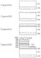
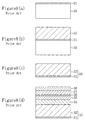
- a silicon crystal is grown by vapor phase epitaxy (hereinafter referred to as CVD) using a gas containing silicon, such as monosilane or dichlorosilane (SiH 2 Cl 2 ), on a substrate 100 made of, e.g., sapphire and having a thickness of 300 ⁇ m to form a strain reducing layer 101 made of silicon and having a thickness of, e.g., 1.5 ⁇ m.
- the substrate 100 is formed to have a main surface having a (0001) plane, whereby the strain reducing layer 101 having a growth interface having a (111) plane is formed.
- the temperature of the substrate 100 is adjusted to 500 °C and MOVPE is performed under a reduced pressure by using, e.g., trimethylgallium, trimethylaluminium, and ammonia as raw material gases to grow an AlN crystal on the strain reducing layer 101 and thereby form an AlN layer 102 having a thickness of, e.g., 0.05 ⁇ m as a buffer layer, as shown in Figure 1(b) .
- the temperature of the substrate 100 is defined as a temperature including the strain reducing layer 101 or the like formed on the substrate 100 .
- the temperature of the substrate 100 is adjusted to 1000 °C and MOVPE is performed under a reduced pressure by using, e.g., trimethylgallium, trimethylaluminium, and ammonia as raw material gases, similarly to the case of forming the AlN layer 102 , to grow a GaN crystal on the AlN layer 102 and thereby form a GaN layer 103 having a thickness of 3.0 ⁇ m as a first contact layer, as shown in Figure 1(c) .
- the GaN layer 103 is doped with an impurity such as Si, Ge, or Se to have the n-type conductivity.
- Table 1 shows the respective thermal expansion coefficients of sapphire, silicon, and GaN.
- the substrate 100 made of sapphire has a thermal expansion coefficient of 7.5 x 10 -6 /K (hereinafter referred to as a first thermal expansion coefficient T1)
- the strain reducing layer 101 made of silicon has a thermal expansion coefficient of 2.55 x 10 -6 /K (hereinafter referred to as a second thermal expansion coefficient T2)
- the GaN layer 103 has a thermal expansion coefficient of 5.59 x 10 -6 /K (hereinafter referred to as a third thermal expansion coefficient T3), as shown in Table 1 .
- the second thermal expansion coefficient T2 is lower than the first thermal expansion coefficient T1
- the third thermal expansion coefficient T3 is lower than the first thermal expansion coefficient T1 and higher than the second thermal expansion coefficient T2.
- a first clad layer 104 made of n-type AlGaN, an active layer 105 made of undoped GaInN, a second clad layer 106 made of p-type AlGaN, and a second contact layer 107 made of p-type GaN are formed successively on the GaN layer 103 .
- a device structure composed of the GaN layer 103 i.e., the first contact layer, the first clad layer 104 , the active layer 105 , the second clad layer 106 , and the second contact layer 107 is partially removed by etching till the GaN layer 103 is etched halfway.
- the temperature of the substrate 100 is lowered from a temperature (about 1000 °C) for the crystal growth of the GaN layer 103 or the like to a room temperature.
- a p-type electrode 109 made of an Ni-Au alloy is formed on the second contact layer 107 with a current restricting layer 108 having an opening 108a interposed therebetween and an n-type electrode 110 made of an Ni-Au alloy is formed in a space corresponding to the etched portion of the GaN layer 103 , i.e., the first contact layer, whereby the laser diode is completed.
- the strain reducing layer 101 having the second thermal expansion coefficient T2 lower than the first thermal expansion coefficient T1 is formed on the substrate 100 having the first thermal expansion coefficient T1 and the GaN layer 103 having the third thermal expansion coefficient T3 lower than the first thermal expansion coefficient T1 and higher than the second thermal expansion coefficient T2 is formed on the strain reducing layer 101 . Accordingly, when the temperature of the substrate 100 is lowered from the temperature for the crystal growth of the GaN layer 103 to a room temperature after the formation of the GaN layer 103 , a compression strain applied from the substrate 100 to the strain reducing layer 101 and a tensile strain applied from the strain reducing layer 101 to the GaN layer 103 cancel out each other.
- the GaN layer 103 having the third thermal expansion coefficient T3 is formed on a multilayer structure composed of the substrate 100 having the first thermal expansion coefficient T1 higher than the third thermal expansion coefficient T3 and the strain reducing layer 101 having the second thermal expansion coefficient T2 lower than the third thermal expansion coefficient T3, the difference between a mean value of the thermal expansion coefficients of the multilayer structure and the third thermal expansion coefficient T3 can be made smaller than the difference between the first and third thermal expansion coefficients T1 and T3. Consequently, the internal stress produced in the GaN layer 103 in response to the compression strain from the substrate 100 is reduced and cracks are less likely to be formed in the GaN layer 103 . This improves the crystalline characteristics of the GaN layer 103 and the crystalline characteristics of the device structure formed on the GaN layer 103 .
- the strain reducing layer 101 Since the first embodiment has formed the strain reducing layer 101 made of silicon on the substrate 100 made of sapphire, the strain reducing layer 101 has a specified growth interface so that the crystalline characteristics of the GaN layer 103 formed on the strain reducing layer 101 are further improved.
- the substrate 100 made of sapphire and having a main surface having a (0001) plane for example, the strain reducing layer 101 made of silicon and having a growth interface having a (111) plane is formed so that the GaN layer 103 with a growth interface having a (0001) plane is formed on the strain reducing layer 101 . This further improves the crystalline characteristics of the GaN layer 103 .
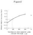
- Figure 2 shows the relationship between the thickness of the strain reducing layer 101 made of silicon and a tensile strain applied from the multilayer structure composed of the substrate 100 and the strain reducing layer 101 to the GaN layer 103 when the temperature of the substrate 100 is lowered from 1000 °C to a room temperature. If the tensile strain represented by the vertical axis in Figure 2 has a negative value, it indicates that the compression strain is applied to the GaN layer 103 . If the thickness of the strain reducing layer 101 , i.e., a silicon thin film represented by the horizontal axis has an infinite value ( ⁇ ), it indicates that the GaN layer 103 has been formed by crystal growth on a substrate composed of silicon in place of the substrate 100 composed of sapphire. The substrate 100 has a thickness of 300 ⁇ m and the GaN layer 103 has a thickness of 3 ⁇ m.
- a compression strain is applied to the GaN layer 103 if the thickness of the strain reducing layer 101 is about 80 ⁇ m or less. If the thickness of the strain reducing layer 101 is more than about 80 ⁇ m, on the other hand, a tensile strain is applied to the GaN layer 103 .
- the reason for this may be that, if the thickness of the strain reducing layer 101 is about 80 ⁇ m or less, the compression strain applied from the substrate 100 to the GaN layer 103 is higher than the tensile strain applied from the strain reducing layer 101 to the GaN layer 103 and, if the thickness of the strain reducing layer 101 is more than about 80 ⁇ m, on the other hand, the compression strain applied from the substrate 100 to the GaN layer 103 is smaller than the tensile strain applied from the strain reducing layer 101 to the GaN layer 103 .
- the thickness of the strain reducing layer 101 i.e., the thickness of the silicon thin film is about 80 ⁇ m, it may be considered that the compression strain applied from the substrate 100 to the GaN layer 103 and the tensile strain applied from the strain reducing layer 101 to the GaN layer 103 are balanced and therefore the strain applied from the multilayer structure composed of the substrate 100 and the strain reducing layer 101 to the GaN layer 103 is minimized.
- the strain reducing layer 101 is preferably formed to have a thickness smaller than the thickness of the substrate 100 .
- the strain reducing layer 101 is preferably formed to have a thickness larger than the thickness of the substrate 100 . The arrangement further reduces the difference between a mean value of the thermal expansion coefficients of the multilayer structure composed of the substrate 100 and the strain reducing layer 101 and the third thermal expansion coefficient T3, so that the crystalline characteristics of the GaN layer 103 are further improved.
- the GaN layer 103 having a thermal expansion coefficient of 5.59 x 10 -6 /K (third thermal expansion coefficient T3) is formed on the substrate 100 made of sapphire having a thermal expansion coefficient of 7.5 x 10 -6 / K (first thermal expansion coefficient T1) with the strain reducing layer 101 made of silicon having a thermal expansion coefficient of 2.55 x 10 -6 /K (second thermal expansion coefficient T2) interposed therebetween, the ratio T1/T3 (about 1.34) of the first thermal expansion coefficient T1 to the third thermal expansion coefficient T3 is lower than the ratio T3/T2 (about 2.19) of the third thermal expansion coefficient T3 to the second thermal expansion coefficient T2, so that the thickness of the strain reducing layer 101 is made smaller than the thickness of the substrate 100 .
- the first embodiment has used the substrate 100 made of sapphire, it is also possible to use instead a substrate made of ZnO (with a thermal expansion coefficient of 8.25 x 10 -6 /K), GaAs (with a thermal expansion coefficient of 6.0 x 10 -6 /K), MgO (with a thermal expansion coefficient of 10.5 x 10 -6 /K), MgAlO 2 (with a thermal expansion coefficient of 7.45 x 10 -6 /K), BeO (with a thermal expansion coefficient of 7.3 x 10 -6 /K), or the like.
- ZnO with a thermal expansion coefficient of 8.25 x 10 -6 /K
- GaAs with a thermal expansion coefficient of 6.0 x 10 -6 /K
- MgO with a thermal expansion coefficient of 10.5 x 10 -6 /K
- MgAlO 2 with a thermal expansion coefficient of 7.45 x 10 -6 /K
- BeO with a thermal expansion coefficient of 7.3 x 10 -6 /K
- the first embodiment has used the strain reducing layer 101 made of silicon, it is also possible to use instead a strain reducing layer made of SiC (with a thermal expansion coefficient of 3.7 x 10 -6 /K), InP (with a thermal expansion coefficient of 4.5 x 10 -6 /K), diamond (with a thermal expansion coefficient of 2.3 x 10 -6 /K), BP (with a thermal expansion coefficient of 3.0 x 10 -6 /K), or the like.
- SiC with a thermal expansion coefficient of 3.7 x 10 -6 /K
- InP with a thermal expansion coefficient of 4.5 x 10 -6 /K
- diamond with a thermal expansion coefficient of 2.3 x 10 -6 /K
- BP with a thermal expansion coefficient of 3.0 x 10 -6 /K
- the present invention is not limited thereto. It is also possible to form a layer made of a nitride compound represented by Al x Ga 1-x N (0 ⁇ x ⁇ 1) as the buffer layer.
- the present invention is not limited thereto. It is also possible to form a semiconductor layer made of a nitride compound represented by Al y Ga 1-y-z In z N (0 ⁇ y ⁇ 1, 0 ⁇ z ⁇ 1) on the strain reducing layer 101 with the buffer layer interposed therebetween by supplying a gallium raw material, an aluminium raw material, and an indium raw material at an appropriate mixing ratio.
- the n-type conductivity to the GaN layer 103 in the first embodiment it is preferable to use a raw material containing a Group IV element or a Group VI element and dope the GaN layer 103 with, as an impurity, a Group IV element such as Si or Ge or a Group VI element such as Se.
- a Group IV element such as Si or Ge or a Group VI element such as Se.
- a Group II element such as Be, Mg, or Zn.
- the first embodiment has formed the strain reducing layer 101 made of silicon on the substrate 100 made of sapphire by crystal growth, it is possible to bond a first substrate made of sapphire and having a specified thickness to a second substrate made of silicon and having a specified thickness. Alternatively, it is also possible to bond a first substrate made of sapphire to a second substrate made of silicon and then polish the first or second substrate to a specified thickness.
- the present invention is not limited thereto. It is also possible to form another device comprising a nitride compound semiconductor layer such as a light-emitting diode or a high-speed transistor.
- the first embodiment has formed the laser diode on the strain reducing layer 101 made of silicon, i.e., on the silicon thin film
- a first device such as an integrated circuit comprising a silicon semiconductor layer on a silicon thin film
- a second device such as a laser diode comprising a nitride compound semiconductor layer on the silicon thin film.
- the arrangement implements an integrated circuit in which an optical function and an electronic function are fused, i.e., an OEIC (optoelectronic IC).
- a first substrate made of, e.g., silicon and having a thickness of 300 ⁇ m and a second substrate made of, e.g., sapphire and a having a thickness of 300 ⁇ m are bonded to each other.
- the first substrate is polished to have a thickness of about 80 ⁇ m such that the second substrate, i.e., a strain reducing layer 201 made of sapphire and a having a thickness of 300 ⁇ m is formed on the first polished substrate, i.e., a substrate 200 made of silicon and having a thickness of about 80 ⁇ m, as shown in Figure 3(a) .
- the temperature of the substrate 200 is adjusted to 500 °C and MOVPE is performed under a reduced pressure by using, e.g., trimethylgallium, trimethylaluminium, and ammonia as raw material gases to grow an AlN crystal on the strain reducing layer 201 and thereby form an AlN layer 202 having a thickness of, e.g., 0.05 ⁇ m as a buffer layer, as shown in Figure 3(b) .
- the temperature of the substrate 200 is defined as a temperature including the strain reducing layer 201 or the like formed on the substrate 200 .
- the temperature of the substrate 200 is adjusted to 1000 °C and MOVPE is performed under a reduced pressure by using, e.g., trimethylgallium, trimethylaluminium, and ammonia as raw material gases, similarly to the case of forming the AlN layer 202 , to grow a GaN crystal on the AlN layer 202 and thereby form a GaN layer 203 having a thickness of 3.0 ⁇ m as a first contact layer, as shown in Figure 3(c) .
- the GaN layer 203 is doped with an impurity such as Si, Ge, or Se to have the n-type conductivity.
- the substrate 200 made of silicon has a thermal expansion coefficient of 2.55 x 10 -6 /K (hereinafter referred to as a first thermal expansion coefficient T1)
- the strain reducing layer 201 made of sapphire has a thermal expansion coefficient of 7.5 x 10 -6 /K (hereinafter referred to as a second thermal expansion coefficient T2)
- the GaN layer 203 has a thermal expansion coefficient of 5.59 x 10 -6 /K (hereinafter referred to as a third thermal expansion coefficient T3), as shown in Table 1 (see EMBODIMENT 1 ).
- the second thermal expansion coefficient T2 is higher than the first thermal expansion coefficient T1
- the third thermal expansion coefficient T3 is higher than the first thermal expansion coefficient T1 and lower than the second thermal expansion coefficient T2.
- a first clad layer 204 made of n-type AlGaN, an active layer 205 made of undoped GaInN, a second clad layer 206 made of p-type AlGaN, and a second contact layer 207 made of p-type GaN are formed successively on the GaN layer 203 .
- a device structure composed of the GaN layer 203 i.e., the first contact layer, the first clad layer 204 , the active layer 205 , the second clad layer 206 , and the second contact layer 207 is partially removed by dry etching till the GaN layer 203 is etched halfway.
- the temperature of the substrate 200 is lowered from a temperature (about 1000 °C) for the crystal growth of the GaN layer 203 to a room temperature.
- a p-type electrode 209 composed of an Ni-Au alloy is formed on the second contact layer 207 with a current restricting layer 208 having an opening 208a interposed therebetween and an n-type electrode 210 composed of an Ni-Au alloy is formed in a space corresponding to the etched portion of the GaN layer 203 , i.e., the first contact layer, whereby the laser diode is completed.
- the strain reducing layer 201 having the second thermal expansion coefficient T2 higher than the first thermal expansion coefficient T1 is formed on the substrate 200 having the first thermal expansion coefficient T1 and the GaN layer 203 having the third thermal expansion coefficient T3 higher than the first thermal expansion coefficient T1 and lower than the second thermal expansion coefficient T2 is formed on the strain reducing layer 201 . Accordingly, when the temperature of the substrate 200 is lowered from the temperature for the crystal growth of the GaN layer 203 to a room temperature after the formation of the GaN layer 203 , a tensile strain applied from the substrate 200 to the strain reducing layer 201 and a compression strain applied from the strain reducing layer 201 to the GaN layer 203 cancel out each other.
- the GaN layer 203 having a third thermal expansion coefficient T3 is formed on a multilayer structure composed of the substrate 200 having the first thermal expansion coefficient T1 lower than the third thermal expansion coefficient T3 and the strain reducing layer 201 having the second thermal expansion coefficient T2 higher than the third thermal expansion coefficient T3, the difference between a mean value of the thermal expansion coefficients of the multilayer structure and the third thermal expansion coefficient T3 can be made smaller than the difference between the first and third thermal expansion coefficients T1 and T3.
- an internal stress produced in the GaN layer 203 in response to the tensile strain from the substrate 200 is reduced and cracks are less likely to be formed in the GaN layer 203 . This improves the crystalline characteristics of the GaN layer 203 and the crystalline characteristics of the device structure formed on the GaN layer 203 .
- the strain reducing layer 201 is preferably formed to have a thickness smaller than the thickness of the substrate 200 .
- the strain reducing layer 201 is preferably formed to have a thickness larger than the thickness of the substrate 200 . This further reduces the difference between a mean value of the thermal expansion coefficients of the multilayer structure composed of the substrate 200 and the strain reducing layer 201 and the third thermal expansion coefficient T3 and further improves the crystalline characteristics of the GaN layer 203 .
- the GaN layer 203 having a thermal expansion coefficient of 5.59 x 10 -6 /K (third thermal expansion coefficient T3) is formed on the substrate 200 made of silicon having a thermal expansion coefficient of 2.55 x 10 -6 /K (first thermal expansion coefficient T1) with the strain reducing layer 201 made of sapphire having a thermal expansion coefficient of 7.5 x 10 -6 /K (second thermal expansion coefficient T2) interposed therebetween, the ratio T3/T1 (about 2.19) of the third thermal expansion coefficient T3 to the first thermal expansion coefficient T1 is higher than the ratio T2/T3 (about 1.34) of the second thermal expansion coefficient T2 to the third thermal expansion coefficient T3, so that the thickness of the strain reducing layer 201 is made larger than the thickness of the substrate 200 .
- the second embodiment has used the substrate 200 made of silicon, it is also possible to use instead a substrate made of SIC (with a thermal expansion coefficient of 3.7 x 10 -6 /K), InP (with a thermal expansion coefficient of 4.5 x 10 -6 /K), diamond (with a thermal expansion coefficient of 2.3 x 10 -6 /K), BP (with a thermal expansion coefficient of 3.0 x 10 -6 /K), or the like.
- SIC with a thermal expansion coefficient of 3.7 x 10 -6 /K
- InP with a thermal expansion coefficient of 4.5 x 10 -6 /K
- diamond with a thermal expansion coefficient of 2.3 x 10 -6 /K
- BP with a thermal expansion coefficient of 3.0 x 10 -6 /K
- the second embodiment has used the strain reducing layer 201 made of sapphire, it is also possible to use instead a strain reducing layer made of ZnO (with a thermal expansion coefficient of 8.25 x 10 -6 /K), GaAs (with a thermal expansion coefficient of 6.0 x 10 -6 /K), MgO (with a thermal expansion coefficient of 10.5 x 10 -6 /K), MgAlO 2 (with a thermal expansion coefficient of 7.45 x 10 -6 /K), BeO (with a thermal expansion coefficient of 7.3 x 10 -6 /K), or the like.
- ZnO with a thermal expansion coefficient of 8.25 x 10 -6 /K
- GaAs with a thermal expansion coefficient of 6.0 x 10 -6 /K
- MgO with a thermal expansion coefficient of 10.5 x 10 -6 /K
- MgAlO 2 with a thermal expansion coefficient of 7.45 x 10 -6 /K
- BeO with a thermal expansion coefficient of 7.3
- the second embodiment has formed the AlN layer 202 as the buffer layer
- the present invention is not limited thereto. It is also possible to form a layer made of a nitride compound represented by Al x Ga 1-x N (0 ⁇ x ⁇ 1) as the buffer layer.
- the present invention is not limited thereto. It is also possible to form a semiconductor layer made of a nitride compound represented by Al y Ga 1-y-z In z N (0 ⁇ y ⁇ 1, 0 ⁇ z ⁇ 1) on the strain reducing layer 201 with the buffer layer interposed therebetween by supplying a gallium raw material, an aluminium raw material, and an indium raw material at an appropriate mixing ratio.
- a Group II element such as Be, Mg, or Zn.
- the second embodiment has bonded the first substrate made of silicon to the second substrate made of sapphire and polished only the first substrate to a specified thickness
- the second embodiment has formed the laser diode having the GaN layer 203 on the multilayer structure composed of the substrate 200 and the strain reducing layer 201 , it is also possible to form instead a GaN thick film on the multilayer structure composed of the substrate 200 and the strain reducing layer 201 , separate the multilayer structure from the GaN thick film to form a semiconductor substrate composed of the GaN thick film, and then form a laser diode on the semiconductor substrate.
- the second embodiment has formed the laser diode comprising the GaN layer 203 and the device structure formed thereon, the present invention is not limited thereto. It is also possible to form another device comprising a nitride compound semiconductor layer such as a light-emitting diode or a high-speed transistor.
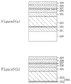
- a silicon crystal is grown by CVD using a gas containing silicon, such as a monosilane or dichlorosilane, on a substrate 300 made of, e.g., sapphire and having a thickness of 300 ⁇ m to form a strain reducing layer 301 made of silicon and having a thickness of, e.g., 80 ⁇ m.
- the substrate 300 is formed to have a main surface having a (0001) plane, whereby the strain reducing layer 301 having a growth interface having a (111) plane is formed.
- the temperature of the substrate 300 is adjusted to 500 °C and MOVPE is performed under a reduced pressure by using, e.g., trimethylgallium, trimethylaluminium, and ammonia as raw material gases to grow an AlN crystal on the strain reducing layer 301 and thereby form an AlN layer 302 having a thickness of, e.g., 0.05 ⁇ m as a buffer layer, as shown in Figure 4(a) .
- the temperature of the substrate 300 is defined as a temperature including the strain reducing layer 301 or the like formed on the substrate 300 .
- the substrate 300 has a circular configuration with a diameter of about 2 inches.
- the temperature of the substrate 300 is adjusted to 1000 °C and hydride VPE (hereinafter referred to as HVPE) is performed under normal pressure by using gallium chloride and ammonia as raw materials to grow a GaN crystal on the AlN layer 302 and thereby form a GaN thick film 303 having a thickness of, e.g., 300 ⁇ m, as shown in Figure 4(b) .
- HVPE hydride VPE
- the temperature of the substrate 300 is lowered from a temperature (1000 °C) for the crystal growth of the GaN thick film 303 to a room temperature.
- Gallium chloride which is used as the raw material in the HVPE process, is generated by bringing a hydrogen chloride gas into contact with a metal gallium heated to 800 °C.
- the substrate 300 made of sapphire has a thermal expansion coefficient of 7.5 x 10 -6 /K (hereinafter referred to as a first thermal expansion coefficient T1)
- the strain reducing layer 301 made of silicon has a thermal expansion coefficient of 2.55 x 10 -6 /K (hereinafter referred to as a second thermal expansion coefficient T2)
- the GaN thick film 303 has a thermal expansion coefficient of 5.59 x 10 -6 /K (hereinafter referred to as a third thermal expansion coefficient T3), as shown in Table 1 (see EMBODIMENT 1).
- the second thermal expansion coefficient T2 is lower than the first thermal expansion coefficient T1
- the third thermal expansion coefficient T3 is lower than the first thermal expansion coefficient T1 and higher than the second thermal expansion coefficient T2.
- the strain reducing layer 301 made of silicon is removed by using a solution containing, e.g., a hydrofluoric acid, a nitric acid, and water at a mixing ratio of 1:1:2, whereby the GaN thick film 303 and the AlN layer 302 are separated from a multilayer structure composed of the substrate 300 and the strain reducing layer 301 to form a semiconductor substrate 304 composed of the GaN thick film 303 and the AlN layer 302 , as shown in Figure 4(c) .
- a solution containing e.g., a hydrofluoric acid, a nitric acid, and water at a mixing ratio of 1:1:2, whereby the GaN thick film 303 and the AlN layer 302 are separated from a multilayer structure composed of the substrate 300 and the strain reducing layer 301 to form a semiconductor substrate 304 composed of the GaN thick film 303 and the AlN layer 302 , as shown in Figure 4(c) .
- a first contact layer 305 made of n-type GaN, a first clad layer 306 made of n-type AlGaN, an active layer 307 made of undoped GaInN, a second clad layer 308 made of p-type AlGaN, and a second contact layer 309 made of p-type GaN are formed successively on the semiconductor substrate 304 .
- a p-type electrode is formed on the second contact layer 309 with a current restricting layer interposed therebetween and an n-type electrode is formed on a back surface of the semiconductor substrate 304 , though they are not depicted, whereby the laser diode is completed.
- the strain reducing layer 301 having the second thermal expansion coefficient T2 lower than the first thermal expansion coefficient T1 is formed on the substrate 300 having the first thermal expansion coefficient T1 and then the GaN thick film 303 having the third thermal expansion coefficient T3 lower than the first thermal expansion coefficient T1 and higher than the second thermal expansion coefficient T2 is formed on the strain reducing layer 301 . Accordingly, when the temperature of the substrate 300 is lowered from a temperature for the crystal growth of the GaN thick film 303 to a room temperature after the formation of the GaN thick film 303 , a compression strain applied from the substrate 300 to the strain reducing layer 301 and a tensile strain applied from the strain reducing layer 301 to the GaN thick film 303 cancel out each other.
- the GaN thick film 303 having the third thermal expansion coefficient T3 is formed on a multilayer structure composed of the substrate 300 having the first thermal expansion coefficient T1 higher than the third thermal expansion coefficient T3 and the strain reducing layer 301 having the second thermal expansion coefficient T2 lower than the third thermal expansion coefficient T3, the difference between a mean value of the thermal expansion coefficients of the multilayer structure and the third thermal expansion coefficient T3 can be made smaller than the difference between the first and third thermal expansion coefficients T1 and T3. Consequently, the internal stress produced in the GaN thick film 303 in response to the compression strain from the substrate 300 is reduced and cracks are less likely to be formed in the GaN thick film 303 . This improves the crystalline characteristics of the GaN thick film 303 . By thus separating the GaN thick film 303 from the multilayer structure composed of the substrate 300 and the strain reducing layer 301 , there can be formed the semiconductor substrate 304 composed of the GaN thick film 303 having excellent crystalline characteristics.
- the compression strain applied from the substrate 300 to the GaN thick film 303 and the tensile strain applied from the strain reducing layer 301 to the GaN thick film 303 are balanced by adjusting the thickness of the substrate 300 made of sapphire to 300 ⁇ m and adjusting the thickness of the strain reducing layer 301 made of silicon to about 80 ⁇ m.
- the third embodiment has formed the GaN thick film 303 on the substrate 300 having a large diameter of about 2 inches, there can be formed the semiconductor substrate 304 composed of the GaN thick film 303 having excellent crystalline characteristics and a large area.
- the strain reducing layer 301 Since the third embodiment has formed the strain reducing layer 301 made of silicon on the substrate 300 made of sapphire, the strain reducing layer 301 has a specified growth interface so that the crystalline characteristics of the GaN thick film 303 formed on the strain reducing layer 301 are further improved.
- the substrate 300 made of sapphire and having a main surface having a (0001) plane for example, the strain reducing layer 301 made of silicon and having a growth interface having a (111) plane is formed so that the GaN thick film 303 having a growth interface having a (0001) plane is formed on the strain reducing layer 301 . This further improves the crystalline characteristics of the GaN thick film 303 .
- the diameter of the semiconductor substrate 304 composed of the GaN thick film 303 was about 2 inches, which is nearly equal to the diameter of the substrate 300 .
- the GaN thick film 303 can be separated from the multilayer structure composed of the substrate 300 and the strain reducing layer 301 without removing the substrate 300 by polishing.
- the semiconductor substrate 304 composed of the GaN thick film 303 can be formed easily in a short period of time and the substrate 300 separated from the GaN thick film 303 can be used again to newly form a GaN thick film.
- the strain reducing layer 301 is preferably formed to have a thickness smaller than the thickness of the substrate 300 .
- the strain reducing layer 301 is preferably formed to have a thickness larger than the thickness of the substrate 300 . This further reduces the difference between a mean value of the thermal expansion coefficients of the multilayer structure composed of the substrate 300 and the strain reducing layer 301 and the third thermal expansion coefficient T3 and further improves the crystalline characteristics of the GaN thick film 303 .
- the GaN thick film 303 having a thermal expansion coefficient of 5.59 x 10 -6 /K (third thermal expansion coefficient T3) is formed on the substrate 300 made of sapphire having a thermal expansion coefficient of 7.5 x 10 -6 / K (first thermal expansion coefficient T1) with the strain reducing layer 301 made of silicon having a thermal expansion coefficient of 2.55 x 10 -6 /K (second thermal expansion coefficient T2) interposed therebetween, the ratio T1/T3 (about 1.34) of the first thermal expansion coefficient T1 to the third thermal expansion coefficient T3 is lower than the ratio T3/T2 (about 2.19) of the third thermal expansion coefficient T3 to the second thermal expansion coefficient T2, so that the thickness of the strain reducing layer 301 is made smaller than the thickness of the substrate 300 .
- the third embodiment has used the substrate 300 made of sapphire, it is also possible to use instead a substrate made of ZnO (with a thermal expansion coefficient of 8.25 x 10 -6 /K), GaAs (with a thermal expansion coefficient of 6.0 x 10 -6 /K), MgO (with a thermal expansion coefficient of 10.5 x 10 -6 /K), MgAlO 2 (with a thermal expansion coefficient of 7.45 x 10 -6 /K), BeO (with a thermal expansion coefficient of 7.3 x 10 -6 /K), or the like.
- ZnO with a thermal expansion coefficient of 8.25 x 10 -6 /K
- GaAs with a thermal expansion coefficient of 6.0 x 10 -6 /K
- MgO with a thermal expansion coefficient of 10.5 x 10 -6 /K
- MgAlO 2 with a thermal expansion coefficient of 7.45 x 10 -6 /K
- BeO with a thermal expansion coefficient of 7.3 x 10 -6 /K
- the third embodiment has used the strain reducing layer 301 made of silicon, it is also possible to use instead a strain reducing layer made of SiC (with a thermal expansion coefficient of 3.7 x 10 -6 /K), InP (with a thermal expansion coefficient of 4.5 x 10 -6 /K), diamond (with a thermal expansion coefficient of 2.3 x 10 -6 /K), BP (with a thermal expansion coefficient of 3.0 x 10 -6 /K), or the like.
- SiC with a thermal expansion coefficient of 3.7 x 10 -6 /K
- InP with a thermal expansion coefficient of 4.5 x 10 -6 /K
- diamond with a thermal expansion coefficient of 2.3 x 10 -6 /K
- BP with a thermal expansion coefficient of 3.0 x 10 -6 /K
- the present invention is not limited thereto. It is also possible to form a layer made of a nitride compound represented by Al x Ga 1-x N (0 ⁇ x ⁇ 1) as the buffer layer.
- the present invention is not limited thereto. It is also possible to form a thick-film semiconductor layer made of a nitride compound represented by Al y Ga 1-y-z In z N (0 ⁇ y ⁇ 1, 0 ⁇ z ⁇ 1) on the strain reducing layer 301 with the buffer layer interposed therebetween by supplying a gallium raw material, an aluminium raw material, and an indium raw material at an appropriate mixing ratio.
- a thick-film semiconductor layer made of a nitride compound represented by Al y Ga 1-y-z In z N (0 ⁇ y ⁇ 1, 0 ⁇ z ⁇ 1)
- the third embodiment has formed the strain reducing layer 301 made of silicon on the substrate 300 made of sapphire by crystal growth, it is possible to bond a first substrate made of sapphire and having a specified thickness to a second substrate made of silicon and having a specified thickness. Alternatively, it is also possible to bond a first substrate made of sapphire to a second substrate made of silicon and then polish the first or second substrate to a specified thickness.
- the third embodiment has removed the strain reducing layer 301 by using the solution containing a hydrofluoric acid and thereby separated the GaN thick film 303 from the multilayer structure composed of the substrate 300 and the strain reducing layer 301 , it is also possible to remove the multilayer structure composed of the substrate 300 and the strain reducing layer 301 by polishing and thereby separate the GaN thick film 303 from the multilayer structure.
- the third embodiment has left the AlN layer 302 at the back surface of the GaN thick film 303 composing the semiconductor substrate 304 , it is also possible to remove the AlN layer 302 .
- the third embodiment has formed the first contact layer 305 made of n-type GaN on the semiconductor substrate 304 , i.e., on the GaN thick film 303 , it is also possible to form the first contact layer in the surface portion of the GaN thick film 303 by doping the surface portion of the Gan thick film 303 with an impurity such as Si, Ge, or Se.
- the present invention is not limited thereto. It is also possible to form another device comprising a nitride compound semiconductor layer such as a light-emitting diode or a high-speed transistor.
- the strain reducing layer 301 , the AlN layer 302 , and the GaN thick film 303 are formed successively on the substrate 300 , as shown in Figures 4(a) and (b). Subsequently, the GaN thick film 303 is separated from the multilayer structure composed of the substrate 300 and the strain reducing layer 301 , as shown in Figure 4(c) . Thereafter, the device structure (the first contact layer 305 , the first clad layer 306 , the active layer 307 , the second clad layer 308 , and the second contact layer 309 ) is formed on the GaN thick film 303 , i.e., on the semiconductor substrate 304 , as shown in Figure 4(d) .
- the strain reducing layer 301 , the AlN layer 302 , and the GaN thick film 303 are formed successively on the substrate 300 , as shown in Figures 4(a) and (b) , similarly to the third embodiment. Then, the same device structure as formed in the third embodiment is formed on the GaN thick film 303 , as shown in Figure 5(a) . Thereafter, the GaN thick film 303 , i.e., the semiconductor substrate 304 and the device structure formed thereon are separated from the multilayer structure composed of the substrate 300 and the strain reducing layer 301 , as shown in Figure 5(b).
- the variation of the third embodiment achieves the same effect as achieved by the third embodiment, except that the timing of forming the device structure is different.
- the strain reducing layer 301 i.e., the silicon crystal layer by using the solution containing a hydrofluoric acid and thereby separate the GaN thick film 303 or the like from the multilayer structure composed of the substrate 300 and the strain reducing layer 301 .
- This obviates the necessity to remove the substrate 300 by polishing.
- the GaN thick film 303 can be separated easily from the multilayer structure composed of the substrate 300 and the strain reducing layer 301 in a short period of time, while the substrate 300 separated from the GaN thick film 303 can be used again to newly form a GaN thick film.
Abstract
Description
- The present invention relates to a semiconductor device comprising a nitride compound semiconductor layer and a method of fabricating the same.
- A nitride compound semiconductor such as GaN, InN, or AlN is a material suitable for use in a blue semiconductor laser device or in a transistor operable at a high speed even at a high temperature.
- There has conventionally been known a technique for the crystal growth of a nitride compound semiconductor on a Si (silicon) substrate (A. Watanabe et al., Journal of Crystal Growth volume 128 (1993) pp. 391-396).
- As a first conventional embodiment, a laser diode comprising a nitride compound semiconductor layer formed on a silicon substrate will be described with reference to Figure 6.
- As shown in Figure 6, an
AlN layer 11 as a buffer layer, aGaN layer 12 as a first contact layer, afirst clad layer 13 made of n-type AlGaN, anactive layer 14 made of undoped GaInN, asecond clad layer 15 made of p-type AlGaN, and asecond contact layer 16 made of p-type GaN are stacked successively in layers on asilicon substrate 10. TheAlN layer 11 is formed by growing an AlN crystal on thesilicon substrate 10. The GaNlayer 12 is formed by growing a GaN crystal on theAlN layer 11 at a temperature of 1050 °C and doped with an impurity such as Si, Ge, or Se to have the n-type conductivity. To form the GaNlayer 12, metal organic vapor phase epitaxial growth (hereinafter referred to as MOVPE) is used. - A p-
type electrode 18 made of an Ni-Au alloy on thesecond contact layer 16 with acurrent restricting layer 17 having an opening of 17a interposed therebetween, while an n-type electrode 19 is formed on a back surface of thesilicon substrate 10. - In the first conventional embodiment, a tensile strain is applied from the
silicon substrate 10 to theGaN layer 12 and an internal stress is produced in theGaN layer 12 in response to the tensile strain when the temperature of thesilicon substrate 10 is lowered from the crystal growth temperature of 1050 °C to a room temperature after the formation of theGaN layer 12. This is because the thermal expansion coefficient (2.55 x 10⁻⁶/K) of Si is lower than the thermal expansion coefficient (5.59 x 10⁻⁶/K) of GaN. The internal stress produced in theGaN layer 12 increases disadvantageously to form a crack (crevice) in theGaN layer 12. Thus, the method for the crystal growth of a nitride compound semiconductor on a silicon substrate is not practical. - Therefore, a technique for the crystal growth of a nitride compound semiconductor on a sapphire substrate has been used instead (U.S. Pat. No. 5,777,350).
- As a second conventional embodiment, a laser diode comprising a nitride compound semiconductor layer formed on a sapphire substrate will be described with reference to Figure 7.
- As shown in Figure 7, an AlN layer 21 as a buffer layer, a
GaN layer 22 as a first contact layer, afirst clad layer 23 made of n-type AlGaN, an active layer 24 made of undoped GaInN, a second clad layer 25 made of p-type AlGaN, and a second contact layer 26 made of p-type GaN are stacked successively in layers on asapphire substrate 20. The AlN layer 21 is formed by growing an AlN crystal on thesapphire substrate 20. The GaNlayer 22 is formed by growing a GaN crystal on the AlN layer 21 by using MOVPE at a temperature of 1050 °C. The GaNlayer 22 is doped with an impurity such as Si, Ge, or Se to have the n-type conductivity. It is to be noted that a device structure composed of theGaN layer 22 as the first contact layer, thefirst clad layer 23, the active layer 24, the second clad layer 25, and the second contact layer 26 has been partially removed by dry etching till theGaN layer 22 is etched halfway. - A p-
type electrode 28 made of an Ni-Au alloy is formed on the second contact layer 26 with a current restricting layer 27 having an opening 27a interposed therebetween, while an n-type electrode 29 made of an Ni-Au alloy is formed in a space corresponding to the etched portion of theGaN layer 22, i.e., the first contact layer. - According to the second conventional embodiment, a crack is less likely to occur in the
GaN layer 22 than in the first conventional embodiment since the difference between the thermal expansion coefficient (7.5 x 10⁻⁶/K) of sapphire (Al2O3) and the thermal expansion coefficient of GaN is smaller than the difference between the thermal expansion coefficient of Si and that of GaN. - In the second conventional embodiment, however, a compression strain is applied from the
sapphire substrate 20 to theGaN layer 22 and an internal stress is produced in theGaN layer 22 in response to the compression strain when the temperature of thesapphire substrate 20 is lowered from the crystal growth temperature of 1050 °C to a room temperature after the formation of theGaN layer 22, since the thermal expansion coefficient of sapphire is higher than that of GaN. This prevents an improvement in the crystalline characteristics of theGaN layer 22 and causes the first problem that it is difficult to reduce an operating current for the laser diode. - The second conventional embodiment also presents the second problem that it is difficult to fabricate a laser diode having a smooth reflecting mirror surface since it is difficult to cleave the
sapphire substrate 20. - To solve the second problem, there has been proposed a technique for forming a semiconductor substrate composed of a thick-film nitride compound semiconductor layer which has been formed by the crystal growth of a nitride compound semiconductor on a sapphire substrate and separated therefrom (Japanese Unexamined Patent Publication No. HEI 7-165498).
- As a third conventional embodiment, a method of forming a laser diode by using a semiconductor substrate composed of a nitride compound semiconductor layer will be described with reference to Figures 8(a) to (d).
- First, as shown in Figure 8(a), an
AlN layer 31 as a buffer layer is formed by growing an AlN crystal on asapphire substrate 30. - Next, as shown in Figure 8(b), a
GaN layer 32 as a compound semiconductor layer is formed by growing a GaN crystal on theAlN layer 31 at a temperature of 1050 °C. - Next, as shown in Figure 8(c), the
AlN layer 31 and theGaN layer 32 are separated from thesapphire substrate 30 by removing thesapphire substrate 30 by polishing, whereby asemiconductor substrate 33 composed of theAlN layer 31 and theGaN layer 32 is formed. - Next, as shown in Figure 8(d), a
first contact layer 34 made of n-type GaN, afirst clad layer 35 made of n-type AlGaN, anactive layer 36 made of undoped GaInN, asecond clad layer 37 made of p-type AlGaN, and asecond contact layer 38 made of p-type GaN are formed successively on thesemiconductor substrate 33. Thereafter, a p-type electrode is formed on thesecond contact layer 38 with a current restricting layer interposed therebetween and an n-type electrode is formed on a back surface of thesemiconductor substrate 33, though they are not depicted, whereby the laser diode is completed. According to the third conventional embodiment, a laser diode having a smooth reflecting mirror surface can be fabricated since thesemiconductor substrate 33 is cleaved easily. - However, the third conventional embodiment has the problem that the crystalline characteristics of the
GaN layer 32 composing thesemiconductor substrate 33 cannot be improved due to the difference between the thermal expansion coefficient of sapphire and that of GaN, similarly to the second conventional embodiment. The third conventional embodiment also has the problem that the crystalline characteristics of the GaN layer are further degraded as the thickness of theGaN layer 32, i.e., the thickness of thesemiconductor substrate 33 is increased. - In view of the foregoing, it is therefore an object of the present invention to improve the crystalline characteristics of a nitride compound semiconductor layer composing a semiconductor device.
- To attain the object, a first semiconductor device according to the present invention comprises: a substrate having a first thermal expansion coefficient T1; a strain reducing layer having a second thermal expansion coefficient T2, the strain reducing layer being formed on the substrate; and a semiconductor layer having a third thermal expansion coefficient T3, the semiconductor layer being formed on the strain reducing layer and made of a nitride compound represented by AlyGa1-y-zInzN (0 ≦ y ≦ 1, 0 ≦ z ≦1), the second thermal expansion coefficient T2 being lower than the first thermal expansion coefficient T1, the third thermal expansion coefficient T3 being lower than the first thermal expansion coefficient T1 and higher than the second thermal expansion coefficient T2.
- In the first semiconductor device, the strain reducing layer having the second thermal expansion coefficient T2 lower than the first thermal expansion coefficient T1 is formed on the substrate having the first thermal expansion coefficient T1 and the nitride compound semiconductor layer having the third thermal expansion coefficient T3 lower than the first thermal expansion coefficient T1 and higher than the second thermal expansion coefficient T2 is formed on the strain reducing layer. Accordingly, when the temperature of the substrate is lowered from a temperature for the crystal growth of the nitride compound semiconductor layer to a room temperature after the formation of the nitride compound semiconductor layer, a compression strain applied from the substrate to the strain reducing layer and a tensile strain applied from the strain reducing layer to the nitride compound semiconductor layer cancel out each other. In other words, since the nitride compound semiconductor layer having the third thermal expansion coefficient T3 is formed on a multilayer structure composed of the substrate having the first thermal expansion coefficient T1 higher than the third thermal expansion coefficient T3 and the strain reducing layer having the second thermal expansion coefficient T2 lower than the third thermal expansion coefficient T3, the difference between a mean value of the thermal expansion coefficients of the multilayer structure and the third thermal expansion coefficient T3 can be made smaller than the difference between the first and third thermal expansion coefficients T1 and T3. As a result, an internal stress produced in the nitride compound semiconductor layer in response to the compression strain from the substrate is reduced and cracks are less likely to be formed in the nitride semiconductor layer, so that the crystalline characteristics of the nitride compound semiconductor layer are improved.
- In the first semiconductor device, a ratio T1/T3 of the first thermal expansion coefficient T1 to the third thermal expansion coefficient T3 is preferably lower than a ratio T3/T2 of the third thermal expansion coefficient T3 to the second thermal expansion coefficient T2 and the substrate is preferably larger in thickness than the strain reducing layer.
- The arrangement further reduces the difference between the mean value of the thermal expansion coefficients of the multilayer structure composed of the substrate and the strain reducing layer and the third thermal expansion coefficient T3, so that the crystalline characteristics of the nitride compound semiconductor layer are further improved.
- In the first semiconductor device, a ratio T1/T3 of the first thermal expansion coefficient T1 to the third thermal expansion coefficient T3 is preferably higher than a ratio T3/T2 of the third thermal expansion coefficient T3 to the second thermal expansion coefficient T2 and the substrate is preferably smaller in thickness than the strain reducing layer.
- The arrangement further reduces the difference between the mean value of the thermal expansion coefficients of the multilayer structure composed of the substrate and the strain reducing layer and the third thermal expansion coefficient T3, so that the crystalline characteristics of the nitride compound semiconductor layer are further improved.
- In the first semiconductor device, the substrate is preferably made of sapphire and the strain reducing layer is preferably made of silicon.
- In the arrangement, the strain reducing layer having a specified growth interface is formed on the substrate, so that the crystalline characteristics of the nitride compound semiconductor layer formed on the strain reducing layer are further improved.
- In this case, the substrate preferably has a main surface having a (0001) plane and the strain reducing layer preferably has a growth interface having a (111) plane.
- In the arrangement, the nitride compound semiconductor layer having a growth interface having a (0001) plane is formed on the strain reducing layer formed to have a growth interface having a (111) plane, so that the crystalline characteristics of the nitride compound semiconductor layer are further improved.
- A second semiconductor device according to the present invention comprises: a substrate having a first thermal expansion coefficient T1; a strain reducing layer having a second thermal expansion coefficient T2, the strain reducing layer being formed on the substrate; and a semiconductor layer having a third thermal expansion coefficient T3, the semiconductor layer being formed on the strain reducing layer and made of a nitride compound represented by AlyGa1-y-zInzN (0 ≦ y ≦ 1, 0 ≦ z ≦1), the second thermal expansion coefficient T2 being higher than the first thermal expansion coefficient T1, the third thermal expansion coefficient T3 being higher than the first thermal expansion coefficient T1 and lower than the second thermal expansion coefficient T2.
- In the second semiconductor device, the strain reducing layer having the second thermal expansion coefficient T2 higher than the first thermal expansion coefficient T1 is formed on the substrate having the first thermal expansion coefficient T1 and the nitride compound semiconductor layer having the third thermal expansion coefficient T3 higher than the first thermal expansion coefficient T1 and lower than the second thermal expansion coefficient T2 is formed on the strain reducing layer. Accordingly, when the temperature of the substrate is lowered from a temperature for the crystal growth of the nitride compound semiconductor layer to a room temperature after the formation of the nitride compound semiconductor layer, a tensile strain applied from the substrate to the strain reducing layer and a compression strain applied from the strain reducing layer to the nitride compound semiconductor layer cancel out each other. In other words, since the nitride compound semiconductor layer having the third thermal expansion coefficient T3 is formed on a multilayer structure composed of the substrate having the first thermal expansion coefficient T1 lower than the third thermal expansion coefficient T3 and the strain reducing layer having the second thermal expansion coefficient T2 higher than the third thermal expansion coefficient T3, the difference between a mean value of the thermal expansion coefficients of the multilayer structure and the third thermal expansion coefficient T3 can be made smaller than the difference between the first and third thermal expansion coefficients T1 and T3. As a result, an internal stress produced in the nitride compound semiconductor layer in response to the tensile stress from the substrate is reduced and cracks are less likely to be formed in the nitride semiconductor layer, so that the crystalline characteristics of the nitride compound semiconductor layer are improved.
- In the second semiconductor device, a ratio T3/T1 of the third thermal expansion coefficient T3 to the first thermal expansion coefficient T1 is preferably lower than a ratio T2/T3 of the second thermal expansion coefficient T2 to the third thermal expansion coefficient T3 and the substrate is preferably larger in thickness than the strain reducing layer.
- The arrangement further reduces the difference between the mean value of the thermal expansion coefficients of the multilayer structure composed of the substrate and the strain reducing layer and the third thermal expansion coefficient T3, so that the crystalline characteristics of the nitride compound semiconductor layer are further improved.
- In the second semiconductor device, a ratio T3/T1 of the third thermal expansion coefficient T3 to the first thermal expansion coefficient T1 is preferably higher than a ratio T2/T3 of the second thermal expansion coefficient T2 to the third thermal expansion coefficient T3 and the substrate is preferably smaller in thickness than the strain reducing layer.
- The arrangement further reduces the difference between the mean value of the thermal expansion coefficients of the multilayer structure composed of the substrate and the strain reducing layer and the third thermal expansion coefficient T3, so that the crystalline characteristics of the nitride compound semiconductor layer are further improved.
- A first method of fabricating a semiconductor device according to the present invention comprises the steps of: forming a strain reducing layer having a second thermal expansion coefficient T2 on a substrate having a first thermal expansion coefficient T1; and forming a semiconductor layer having a third thermal expansion coefficient T3 on the strain reducing layer, the semiconductor layer being made of a nitride compound represented by AlyGa1-y-zInzN (0 ≦ y ≦ 1, 0 ≦ z ≦1), the second thermal expansion coefficient T2 being lower than the first thermal expansion coefficient T1, the third thermal expansion coefficient T3 being lower than the first thermal expansion coefficient T1 and higher than the second thermal expansion coefficient T2.
- In the first method of fabricating a semiconductor device, the strain reducing layer having the second thermal expansion coefficient T2 lower than the first thermal expansion coefficient T1 is formed on the substrate having the first thermal expansion coefficient T1 and then the nitride compound semiconductor layer having the third thermal expansion coefficient T3 lower than the first thermal expansion coefficient T1 and higher than the second thermal expansion coefficient T2 is formed on the strain reducing layer. Accordingly, when the temperature of the substrate is lowered from a temperature for the crystal growth of the nitride compound semiconductor layer to a room temperature after the formation of the nitride compound semiconductor layer, a compression strain applied from the substrate to the strain reducing layer and a tensile strain applied from the strain reducing layer to the nitride compound semiconductor layer cancel out each other. In other words, since the nitride compound semiconductor layer having the third thermal expansion coefficient T3 is formed on a multilayer structure composed of the substrate having the first thermal expansion coefficient T1 higher than the third thermal expansion coefficient T3 and the strain reducing layer having the second thermal expansion coefficient T2 lower than the third thermal expansion coefficient T3, the difference between a mean value of the thermal expansion coefficients of the multilayer structure and the third thermal expansion coefficient T3 can be made smaller than the difference between the first and third thermal expansion coefficients T1 and T3. As a result, an internal stress produced in the nitride compound semiconductor layer in response to the compression strain from the substrate is reduced and cracks are less likely to be formed in the nitride semiconductor layer, so that the crystalline characteristics of the nitride compound semiconductor layer are improved.
- In the first method of fabricating a semiconductor device, the step of forming the strain reducing layer preferably includes the step of forming, when a ratio T1/T3 of the first thermal expansion coefficient T1 to the third thermal expansion coefficient T3 is lower than a ratio T3/T2 of the third thermal expansion coefficient T3 to the second thermal expansion coefficient T2, the strain reducing layer such that the strain reducing layer is smaller in thickness than the substrate and forming, when the ratio T1/T3 of the first thermal expansion coefficient T1 to the third thermal expansion coefficient T3 is higher than the ratio T3/T2 of the third thermal expansion coefficient T3 to the second thermal expansion coefficient T2, the strain reducing layer such that the strain reducing layer is larger in thickness than the substrate.
- The arrangement further reduces the difference between the mean value of the thermal expansion coefficients of the multilayer structure composed of the substrate and the strain reducing layer and the third thermal expansion coefficient T3, so that the crystalline characteristics of the nitride compound semiconductor layer are further improved.
- In the first method of fabricating a semiconductor device, the substrate is preferably made of sapphire and the strain reducing layer is preferably made of silicon.
- In the arrangement, the strain reducing layer having a specified growth interface is formed on the substrate, so that the crystalline characteristics of the nitride compound semiconductor layer formed on the strain reducing layer are further improved.
- In this case, the step of forming the strain reducing layer preferably includes the step of forming the strain reducing layer having a growth interface having a (111) plane on the substrate having a main surface having a (0001) plane.
- In the arrangement, the nitride compound semiconductor layer having a growth interface having a (0001) plane is formed on the strain reducing layer formed to have a growth interface having a (111) plane, so that the crystalline characteristics of the nitride compound semiconductor layer are further improved.
- A second method of fabricating a semiconductor device according to the present invention comprises the steps of: forming a strain reducing layer having a second thermal expansion coefficient T2 on a substrate having a first thermal expansion coefficient T1; and forming a semiconductor layer having a third thermal expansion coefficient T3 on the strain reducing layer, the semiconductor layer being made of a nitride compound represented by AlyGa1-y-zInzN (0 ≦ y ≦ 1, 0 ≦ z ≦1), the second thermal expansion coefficient T2 being higher than the first thermal expansion coefficient T1, the third thermal expansion coefficient T3 being higher than the first thermal expansion coefficient T1 and lower than the second thermal expansion coefficient T2.
- In the second method of fabricating a semiconductor device, the strain reducing layer having the second thermal expansion coefficient T2 higher than the first thermal expansion coefficient T1 is formed on the substrate having the first thermal expansion coefficient T1 and then the nitride compound semiconductor layer having the third thermal expansion coefficient T3 higher than the first thermal expansion coefficient T1 and lower than the second thermal expansion coefficient T2 is formed on the strain reducing layer. Accordingly, when the temperature of the substrate is lowered from a temperature for the crystal growth of the nitride compound semiconductor layer to a room temperature after the formation of the nitride compound semiconductor layer, a tensile strain applied from the substrate to the strain reducing layer and a compression strain applied from the strain reducing layer to the nitride compound semiconductor layer cancel out each other. In other words, since the nitride compound semiconductor layer having the third thermal expansion coefficient T3 is formed on a multilayer structure composed of the substrate having the first thermal expansion coefficient T1 lower than the third thermal expansion coefficient T3 and the strain reducing layer having the second thermal expansion coefficient T2 higher than the third thermal expansion coefficient T3, the difference between a mean value of the thermal expansion coefficients of the multilayer structure and the third thermal expansion coefficient T3 can be made smaller than the difference between the first and third thermal expansion coefficients T1 and T3. As a result, an internal stress produced in the nitride compound semiconductor layer in response to the tensile stress from the substrate is reduced and cracks are less likely to be formed in the nitride semiconductor layer, so that the crystalline characteristics of the nitride compound semiconductor layer are improved.
- In the second method of fabricating a semiconductor device, the step of forming the strain reducing layer preferably includes the step of forming, when a ratio T3/T1 of the third thermal expansion coefficient T3 to the first thermal expansion coefficient T1 is lower than a ratio T2/T3 of the second thermal expansion coefficient T2 to the third thermal expansion coefficient T3, the strain reducing layer such that the strain reducing layer is smaller in thickness than the substrate and forming, when the ratio T3/T1 of the third thermal expansion coefficient T3 to the first thermal expansion coefficient T1 is higher than the ratio T2/T3 of the second thermal expansion coefficient T2 to the third thermal expansion coefficient T3, the strain reducing layer such that the strain reducing layer is larger in thickness than the substrate.
- The arrangement further reduces the difference between the mean value of the thermal expansion coefficients of the multilayer structure composed of the substrate and the strain reducing layer and the third thermal expansion coefficient T3, so that the crystalline characteristics of the nitride compound semiconductor layer are further improved.
- A third method of fabricating a semiconductor device according to the present invention comprises the steps of: forming a strain reducing layer having a second thermal expansion coefficient T2 on a substrate having a first thermal expansion coefficient T1; forming a semiconductor layer having a third thermal expansion coefficient T3 on the strain reducing layer, the semiconductor layer being made of a nitride compound represented by AlyGa1-y-zInzN (0 ≦ y ≦ 1, 0 ≦ z ≦1); and separating the nitride compound semiconductor layer from a multilayer structure composed of the substrate and the strain reducing layer to form a semiconductor substrate composed of the nitride compound semiconductor layer, the second thermal expansion coefficient T2 being lower than the first thermal expansion coefficient T1, the third thermal expansion coefficient T3 being lower than the first thermal expansion coefficient T1 and higher than the second thermal expansion coefficient T2.
- In the third method of fabricating a semiconductor device, the strain reducing layer having the second thermal expansion coefficient T2 lower than the first thermal expansion coefficient T1 is formed on the substrate having the first thermal expansion coefficient T1 and then the nitride compound semiconductor layer having the third thermal expansion coefficient T3 lower than the first thermal expansion coefficient T1 and higher than the second thermal expansion coefficient T2 is formed on the strain reducing layer. Accordingly, when the temperature of the substrate is lowered from a temperature for the crystal growth of the nitride compound semiconductor layer to a room temperature after the formation of the nitride compound semiconductor layer, a compression strain applied from the substrate to the strain reducing layer and a tensile strain applied from the strain reducing layer to the nitride compound semiconductor layer cancel out each other. In other words, since the nitride compound semiconductor layer having the third thermal expansion coefficient T3 is formed on a multilayer structure composed of the substrate having the first thermal expansion coefficient T1 higher than the third thermal expansion coefficient T3 and the strain reducing layer having the second thermal expansion coefficient T2 lower than the third thermal expansion coefficient T3, the difference between a mean value of the thermal expansion coefficients of the multilayer structure and the third thermal expansion coefficient T3 can be made smaller than the difference between the first and third thermal expansion coefficients T1 and T3. As a result, an internal stress produced in the nitride compound semiconductor layer in response to the compression strain from the substrate is reduced and cracks are less likely to be formed in the nitride semiconductor layer, so that the crystalline characteristics of the nitride compound semiconductor layer are improved. By separating the nitride compound semiconductor layer from the multilayer structure composed of the substrate and the strain reducing layer, therefore, the semiconductor substrate composed of the nitride semiconductor layer with excellent crystalline characteristics can be formed.
- In the third method of fabricating a semiconductor device, the step of forming the strain reducing layer preferably includes the step of forming, when a ratio T1/T3 of the first thermal expansion coefficient T1 to the third thermal expansion coefficient T3 is lower than a ratio T3/T2 of the third thermal expansion coefficient T3 to the second thermal expansion coefficient T2, the strain reducing layer such that the strain reducing layer is smaller in thickness than the substrate and forming, when the ratio T1/T3 of the first thermal expansion coefficient T1 to the third thermal expansion coefficient T3 is higher than the ratio T3/T2 of the third thermal expansion coefficient T3 to the second thermal expansion coefficient T2, the strain reducing layer such that the strain reducing layer is larger in thickness than the substrate.
- The arrangement further reduces the difference between the mean value of the thermal expansion coefficients of the multilayer structure composed of the substrate and the strain reducing layer and the third thermal expansion coefficient T3, so that the crystalline characteristics of the nitride compound semiconductor layer are further improved.
- In the third method of fabricating a semiconductor device, the substrate is preferably made of sapphire and the strain reducing layer is preferably made of silicon.
- In the arrangement, the strain reducing layer having a specified growth interface is formed on the substrate, so that the crystalline characteristics of the nitride compound semiconductor layer formed on the strain reducing layer are further improved.
- In this case, the step of forming the strain reducing layer preferably includes the step of forming the strain reducing layer having a growth interface having a (111) plane on the substrate having a main surface having a (0001) plane.
- In the arrangement, the nitride compound semiconductor layer having a growth interface having a (0001) plane is formed on the strain reducing layer formed to have a growth interface having a (111) plane, so that the crystalline characteristics of the nitride compound semiconductor layer are further improved.
- In this case, the step of forming the semiconductor substrate preferably includes the step of removing the strain reducing layer by using a solution containing a hydrofluoric acid.
- The arrangement allows the nitride compound semiconductor layer to be separated from the multilayer structure composed of the substrate and the strain reducing layer without removing the substrate by polishing. Accordingly, the semiconductor substrate composed of the nitride compound semiconductor layer can be formed easily in a short period of time and the substrate separated from the nitride compound semiconductor layer can be used again to newly form a nitride compound semiconductor layer.
- A fourth method of fabricating a semiconductor device according to the present invention comprises the steps of: forming a strain reducing layer having a second thermal expansion coefficient T2 on a substrate having a first thermal expansion coefficient T1; forming a semiconductor layer having a third thermal expansion coefficient T3 on the strain reducing layer, the semiconductor layer being made of a nitride compound represented by AlyGa1-y-zInzN (0 ≦ y ≦ 1, 0 ≦ z ≦1); and separating the nitride compound semiconductor layer from a multilayer structure composed of the substrate and the strain reducing layer to form a semiconductor substrate composed of the nitride compound semiconductor layer, the second thermal expansion coefficient T2 being higher than the first thermal expansion coefficient T1, the third thermal expansion coefficient T3 being higher than the first thermal expansion coefficient T1 and lower than the second thermal expansion coefficient T2.
- In the fourth method of fabricating a semiconductor device, the strain reducing layer having the second thermal expansion coefficient T2 higher than the first thermal expansion coefficient T1 is formed on the substrate having the first thermal expansion coefficient T1 and then the nitride compound semiconductor layer having the third thermal expansion coefficient T3 higher than the first thermal expansion coefficient T1 and lower than the second thermal expansion coefficient T2 is formed on the strain reducing layer. Accordingly, when the temperature of the substrate is lowered from a temperature for the crystal growth of the nitride compound semiconductor layer to a room temperature after the formation of the nitride compound semiconductor layer, a tensile strain applied from the substrate to the strain reducing layer and a compression strain applied from the strain reducing layer to the nitride compound semiconductor layer cancel out each other. In other words, since the nitride compound semiconductor layer having the third thermal expansion coefficient T3 is formed on a multilayer structure composed of the substrate having the first thermal expansion coefficient T1 lower than the third thermal expansion coefficient T3 and the strain reducing layer having the second thermal expansion coefficient T2 higher than the third thermal expansion coefficient T3, the difference between a mean value of the thermal expansion coefficients of the multilayer structure and the third thermal expansion coefficient T3 can be made smaller than the difference between the first and third thermal expansion coefficients T1 and T3. As a result, an internal stress produced in the nitride compound semiconductor layer in response to the tensile stress from the substrate is reduced and cracks are less likely to be formed in the nitride semiconductor layer, so that the crystalline characteristics of the nitride compound semiconductor layer are improved. By separating the nitride compound semiconductor layer from the multilayer structure composed of the substrate and the strain reducing layer, therefore, the semiconductor substrate composed of the nitride semiconductor layer with excellent crystalline characteristics can be formed.
- In the fourth method of fabricating a semiconductor device, the step of forming the strain reducing layer preferably includes the step of forming, when a ratio T3/T1 of the third thermal expansion coefficient T3 to the first thermal expansion coefficient T1 is lower than a ratio T2/T3 of the second thermal expansion coefficient T2 to the third thermal expansion coefficient T3, the strain reducing layer such that the strain reducing layer is smaller in thickness than the substrate and forming, when the ratio T3/T1 of the third thermal expansion coefficient T3 to the first thermal expansion coefficient T1 is higher than the ratio T2/T3 of the second thermal expansion coefficient T2 to the third thermal expansion coefficient T3, the strain reducing layer such that the strain reducing layer is larger in thickness than the substrate.
- The arrangement further reduces the difference between the mean value of the thermal expansion coefficients of the multilayer structure composed of the substrate and the strain reducing layer and the third thermal expansion coefficient T3, so that the crystalline characteristics of the nitride compound semiconductor layer are further improved.
-
- Figures 1(a) to (d) are cross-sectional views illustrating the individual process steps of a method of fabricating a semiconductor device according to a first embodiment of the present invention;
- Figure 2 shows the relationship between the thickness of a strain reducing layer made of silicon and a strain applied from a multilayer structure composed of a substrate and the strain reducing layer to a GaN layer in the semiconductor device according to the first embodiment;
- Figures 3(a) to (d) are cross-sectional views illustrating the individual process steps of a method of fabricating a semiconductor device according to a second embodiment of the present invention;
- Figures 4(a) to (d) are cross-sectional views illustrating the individual process steps of a method of fabricating a semiconductor device according to a third embodiment of the present invention;
- Figures 5(a) and (b) are cross-sectional views illustrating the individual process steps of a method of fabricating a semiconductor device according to a variation of the third embodiment;
- Figure 6 is a cross-sectional view of a semiconductor device according to a first conventional embodiment;
- Figure 7 is a cross-sectional view of a semiconductor device according to a second conventional embodiment; and
- Figures 8(a) to (d) are cross-sectional views illustrating the individual process steps of a method of fabricating the semiconductor device according to a third conventional embodiment.
-
- Referring now to Figures 1(a) to (d), a description will be given to a semiconductor device and a method of fabricating the same according to a first embodiment of the present invention by using a laser diode as an example.
- First, as shown in Figure 1(a), a silicon crystal is grown by vapor phase epitaxy (hereinafter referred to as CVD) using a gas containing silicon, such as monosilane or dichlorosilane (SiH2Cl2), on a
substrate 100 made of, e.g., sapphire and having a thickness of 300 µm to form astrain reducing layer 101 made of silicon and having a thickness of, e.g., 1.5 µm. At this time, thesubstrate 100 is formed to have a main surface having a (0001) plane, whereby thestrain reducing layer 101 having a growth interface having a (111) plane is formed. - Next, the temperature of the
substrate 100 is adjusted to 500 °C and MOVPE is performed under a reduced pressure by using, e.g., trimethylgallium, trimethylaluminium, and ammonia as raw material gases to grow an AlN crystal on thestrain reducing layer 101 and thereby form anAlN layer 102 having a thickness of, e.g., 0.05 µm as a buffer layer, as shown in Figure 1(b). In the first embodiment, the temperature of thesubstrate 100 is defined as a temperature including thestrain reducing layer 101 or the like formed on thesubstrate 100. - Then, the temperature of the
substrate 100 is adjusted to 1000 °C and MOVPE is performed under a reduced pressure by using, e.g., trimethylgallium, trimethylaluminium, and ammonia as raw material gases, similarly to the case of forming theAlN layer 102, to grow a GaN crystal on theAlN layer 102 and thereby form aGaN layer 103 having a thickness of 3.0 µm as a first contact layer, as shown in Figure 1(c). TheGaN layer 103 is doped with an impurity such as Si, Ge, or Se to have the n-type conductivity. - Table 1 shows the respective thermal expansion coefficients of sapphire, silicon, and GaN.
THERMAL EXPANSION COEFFICIENT (x 10-6/K) SAPPHIRE 7.5 SILICON 2.55 GaN 5.59 - In the first embodiment, the
substrate 100 made of sapphire has a thermal expansion coefficient of 7.5 x 10⁻⁶/K (hereinafter referred to as a first thermal expansion coefficient T1), thestrain reducing layer 101 made of silicon has a thermal expansion coefficient of 2.55 x 10⁻⁶/K (hereinafter referred to as a second thermal expansion coefficient T2), and theGaN layer 103 has a thermal expansion coefficient of 5.59 x 10⁻⁶/K (hereinafter referred to as a third thermal expansion coefficient T3), as shown in Table 1. Briefly, the second thermal expansion coefficient T2 is lower than the first thermal expansion coefficient T1 and the third thermal expansion coefficient T3 is lower than the first thermal expansion coefficient T1 and higher than the second thermal expansion coefficient T2. - Next, as shown in Figure 1(d), a first
clad layer 104 made of n-type AlGaN, anactive layer 105 made of undoped GaInN, a secondclad layer 106 made of p-type AlGaN, and asecond contact layer 107 made of p-type GaN are formed successively on theGaN layer 103. Subsequently, a device structure composed of theGaN layer 103, i.e., the first contact layer, the firstclad layer 104, theactive layer 105, the secondclad layer 106, and thesecond contact layer 107 is partially removed by etching till theGaN layer 103 is etched halfway. After the formation of the device structure, the temperature of thesubstrate 100 is lowered from a temperature (about 1000 °C) for the crystal growth of theGaN layer 103 or the like to a room temperature. Thereafter, a p-type electrode 109 made of an Ni-Au alloy is formed on thesecond contact layer 107 with a current restrictinglayer 108 having anopening 108a interposed therebetween and an n-type electrode 110 made of an Ni-Au alloy is formed in a space corresponding to the etched portion of theGaN layer 103, i.e., the first contact layer, whereby the laser diode is completed. - According to the first embodiment, as described above, the
strain reducing layer 101 having the second thermal expansion coefficient T2 lower than the first thermal expansion coefficient T1 is formed on thesubstrate 100 having the first thermal expansion coefficient T1 and theGaN layer 103 having the third thermal expansion coefficient T3 lower than the first thermal expansion coefficient T1 and higher than the second thermal expansion coefficient T2 is formed on thestrain reducing layer 101. Accordingly, when the temperature of thesubstrate 100 is lowered from the temperature for the crystal growth of theGaN layer 103 to a room temperature after the formation of theGaN layer 103, a compression strain applied from thesubstrate 100 to thestrain reducing layer 101 and a tensile strain applied from thestrain reducing layer 101 to theGaN layer 103 cancel out each other. In other words, since theGaN layer 103 having the third thermal expansion coefficient T3 is formed on a multilayer structure composed of thesubstrate 100 having the first thermal expansion coefficient T1 higher than the third thermal expansion coefficient T3 and thestrain reducing layer 101 having the second thermal expansion coefficient T2 lower than the third thermal expansion coefficient T3, the difference between a mean value of the thermal expansion coefficients of the multilayer structure and the third thermal expansion coefficient T3 can be made smaller than the difference between the first and third thermal expansion coefficients T1 and T3. Consequently, the internal stress produced in theGaN layer 103 in response to the compression strain from thesubstrate 100 is reduced and cracks are less likely to be formed in theGaN layer 103. This improves the crystalline characteristics of theGaN layer 103 and the crystalline characteristics of the device structure formed on theGaN layer 103. - Since the first embodiment has formed the
strain reducing layer 101 made of silicon on thesubstrate 100 made of sapphire, thestrain reducing layer 101 has a specified growth interface so that the crystalline characteristics of theGaN layer 103 formed on thestrain reducing layer 101 are further improved. By forming thesubstrate 100 made of sapphire and having a main surface having a (0001) plane, for example, thestrain reducing layer 101 made of silicon and having a growth interface having a (111) plane is formed so that theGaN layer 103 with a growth interface having a (0001) plane is formed on thestrain reducing layer 101. This further improves the crystalline characteristics of theGaN layer 103. - The foregoing effect will be described in greater detail with reference to Figure 2.
- Figure 2 shows the relationship between the thickness of the
strain reducing layer 101 made of silicon and a tensile strain applied from the multilayer structure composed of thesubstrate 100 and thestrain reducing layer 101 to theGaN layer 103 when the temperature of thesubstrate 100 is lowered from 1000 °C to a room temperature. If the tensile strain represented by the vertical axis in Figure 2 has a negative value, it indicates that the compression strain is applied to theGaN layer 103. If the thickness of thestrain reducing layer 101, i.e., a silicon thin film represented by the horizontal axis has an infinite value (∞), it indicates that theGaN layer 103 has been formed by crystal growth on a substrate composed of silicon in place of thesubstrate 100 composed of sapphire. Thesubstrate 100 has a thickness of 300 µm and theGaN layer 103 has a thickness of 3 µm. - As shown in Figure 2, a compression strain is applied to the
GaN layer 103 if the thickness of thestrain reducing layer 101 is about 80 µm or less. If the thickness of thestrain reducing layer 101 is more than about 80 µm, on the other hand, a tensile strain is applied to theGaN layer 103. The reason for this may be that, if the thickness of thestrain reducing layer 101 is about 80 µm or less, the compression strain applied from thesubstrate 100 to theGaN layer 103 is higher than the tensile strain applied from thestrain reducing layer 101 to theGaN layer 103 and, if the thickness of thestrain reducing layer 101 is more than about 80 µm, on the other hand, the compression strain applied from thesubstrate 100 to theGaN layer 103 is smaller than the tensile strain applied from thestrain reducing layer 101 to theGaN layer 103. - If the thickness of the
strain reducing layer 101, i.e., the thickness of the silicon thin film is about 80 µm, it may be considered that the compression strain applied from thesubstrate 100 to theGaN layer 103 and the tensile strain applied from thestrain reducing layer 101 to theGaN layer 103 are balanced and therefore the strain applied from the multilayer structure composed of thesubstrate 100 and thestrain reducing layer 101 to theGaN layer 103 is minimized. - As a result of examining, by surface observation using an optical microscope, variations in the number of cracks formed in the
GaN layer 103 when the thickness of thestrain reducing layer 101, i.e., the thickness of the silicon thin film was varied in a semiconductor device comprising theGaN layer 103 shown in Figure 1(c), it was found that cracks were barely formed in theGaN layer 103 when the thickness of thestrain reducing layer 101 is about 100 µm or less and that cracks are formed in theGaN layer 103 when the thickness of thestrain reducing layer 101 is more than about 100 µm and the number of cracks formed in theGaN layer 103 increased as the thickness of thestrain reducing layer 101 increased. - From the result of examination, it can be considered that cracks are less likely to be formed when the compression strain is applied to the
GaN layer 103 formed on thestrain reducing layer 101, i.e., the silicon thin film and that, when the tensile strain is applied to theGaN layer 103, cracks are more likely to be formed and the number of cracks increases as the tensile strain increases. - In the first embodiment, if the ratio T1/T3 of the first thermal expansion coefficient T1 (substrate 100) to the third thermal expansion coefficient T3 (GaN layer 103) is lower than the ratio T3/T2 of the third thermal expansion coefficient T3 to the second thermal expansion coefficient T2 (strain reducing layer 101), the
strain reducing layer 101 is preferably formed to have a thickness smaller than the thickness of thesubstrate 100. Conversely, if the ratio T1/T3 of the first thermal expansion coefficient T1 to the thermal expansion coefficient T3 is higher than the ratio T3/T2 of the third thermal expansion coefficient T3 to the second thermal expansion coefficient T2, thestrain reducing layer 101 is preferably formed to have a thickness larger than the thickness of thesubstrate 100. The arrangement further reduces the difference between a mean value of the thermal expansion coefficients of the multilayer structure composed of thesubstrate 100 and thestrain reducing layer 101 and the third thermal expansion coefficient T3, so that the crystalline characteristics of theGaN layer 103 are further improved. - Specifically, since the
GaN layer 103 having a thermal expansion coefficient of 5.59 x 10⁻⁶/K (third thermal expansion coefficient T3) is formed on thesubstrate 100 made of sapphire having a thermal expansion coefficient of 7.5 x 10⁻⁶/ K (first thermal expansion coefficient T1) with thestrain reducing layer 101 made of silicon having a thermal expansion coefficient of 2.55 x 10⁻⁶/K (second thermal expansion coefficient T2) interposed therebetween, the ratio T1/T3 (about 1.34) of the first thermal expansion coefficient T1 to the third thermal expansion coefficient T3 is lower than the ratio T3/T2 (about 2.19) of the third thermal expansion coefficient T3 to the second thermal expansion coefficient T2, so that the thickness of thestrain reducing layer 101 is made smaller than the thickness of thesubstrate 100. At this time, if thesubstrate 100 has a thickness of, e.g., 300 µm, the formation of thestrain reducing layer 101 having a thickness of about 100 µm or less surely improves the crystalline characteristics of theGaN layer 103. If the thickness of thestrain reducing layer 101 is adjusted to 80 µ m or less, in particular, it becomes possible to prevent the tensile strain from being applied from the multilayer structure composed of thesubstrate 100 and thestrain reducing layer 101 to the GaN layer 103 (see Figure 2), so that the formation of cracks in theGaN layer 103 is prevented reliably. - Although the first embodiment has used the
substrate 100 made of sapphire, it is also possible to use instead a substrate made of ZnO (with a thermal expansion coefficient of 8.25 x 10⁻⁶/K), GaAs (with a thermal expansion coefficient of 6.0 x 10⁻⁶/K), MgO (with a thermal expansion coefficient of 10.5 x 10⁻⁶/K), MgAlO2 (with a thermal expansion coefficient of 7.45 x 10⁻⁶/K), BeO (with a thermal expansion coefficient of 7.3 x 10⁻⁶/K), or the like. - Although the first embodiment has used the
strain reducing layer 101 made of silicon, it is also possible to use instead a strain reducing layer made of SiC (with a thermal expansion coefficient of 3.7 x 10⁻⁶/K), InP (with a thermal expansion coefficient of 4.5 x 10⁻⁶/K), diamond (with a thermal expansion coefficient of 2.3 x 10⁻⁶/K), BP (with a thermal expansion coefficient of 3.0 x 10⁻⁶/K), or the like. - Although the first embodiment has formed the
AlN layer 102 as the buffer layer, the present invention is not limited thereto. It is also possible to form a layer made of a nitride compound represented by AlxGa1-xN (0 < x ≦ 1) as the buffer layer. - Although the first embodiment has formed the
GaN layer 103 on thestrain reducing layer 101 with the buffer layer interposed therebetween, the present invention is not limited thereto. It is also possible to form a semiconductor layer made of a nitride compound represented by AlyGa1-y-zInzN (0 ≦ y ≦ 1, 0 ≦ z ≦1) on thestrain reducing layer 101 with the buffer layer interposed therebetween by supplying a gallium raw material, an aluminium raw material, and an indium raw material at an appropriate mixing ratio. - In the case of imparting the n-type conductivity to the
GaN layer 103 in the first embodiment, it is preferable to use a raw material containing a Group IV element or a Group VI element and dope theGaN layer 103 with, as an impurity, a Group IV element such as Si or Ge or a Group VI element such as Se. In the case of imparting the p-type conductivity to theGaN layer 103, it is preferable to use a raw material containing a Group II element and dope theGaN layer 103 with, as an impurity, a Group II element such as Be, Mg, or Zn. - Although the first embodiment has formed the
strain reducing layer 101 made of silicon on thesubstrate 100 made of sapphire by crystal growth, it is possible to bond a first substrate made of sapphire and having a specified thickness to a second substrate made of silicon and having a specified thickness. Alternatively, it is also possible to bond a first substrate made of sapphire to a second substrate made of silicon and then polish the first or second substrate to a specified thickness. - Although the first embodiment has formed the laser diode comprising the
GaN layer 103 and the device structure formed thereon, the present invention is not limited thereto. It is also possible to form another device comprising a nitride compound semiconductor layer such as a light-emitting diode or a high-speed transistor. - Although the first embodiment has formed the laser diode on the
strain reducing layer 101 made of silicon, i.e., on the silicon thin film, it is also possible to selectively form a first device such as an integrated circuit comprising a silicon semiconductor layer on a silicon thin film and a second device such as a laser diode comprising a nitride compound semiconductor layer on the silicon thin film. The arrangement implements an integrated circuit in which an optical function and an electronic function are fused, i.e., an OEIC (optoelectronic IC). - Referring to Figures 3(a) to (d), a description will be given to a semiconductor device and a method of fabricating the same according to a second embodiment of the present invention by using a laser diode as an example.
- First, a first substrate made of, e.g., silicon and having a thickness of 300 µm and a second substrate made of, e.g., sapphire and a having a thickness of 300 µm are bonded to each other. Then, the first substrate is polished to have a thickness of about 80 µm such that the second substrate, i.e., a
strain reducing layer 201 made of sapphire and a having a thickness of 300 µm is formed on the first polished substrate, i.e., asubstrate 200 made of silicon and having a thickness of about 80 µm, as shown in Figure 3(a). - Next, the temperature of the
substrate 200 is adjusted to 500 °C and MOVPE is performed under a reduced pressure by using, e.g., trimethylgallium, trimethylaluminium, and ammonia as raw material gases to grow an AlN crystal on thestrain reducing layer 201 and thereby form anAlN layer 202 having a thickness of, e.g., 0.05 µm as a buffer layer, as shown in Figure 3(b). In the second embodiment, the temperature of thesubstrate 200 is defined as a temperature including thestrain reducing layer 201 or the like formed on thesubstrate 200. - Then, the temperature of the
substrate 200 is adjusted to 1000 °C and MOVPE is performed under a reduced pressure by using, e.g., trimethylgallium, trimethylaluminium, and ammonia as raw material gases, similarly to the case of forming theAlN layer 202, to grow a GaN crystal on theAlN layer 202 and thereby form aGaN layer 203 having a thickness of 3.0 µm as a first contact layer, as shown in Figure 3(c). TheGaN layer 203 is doped with an impurity such as Si, Ge, or Se to have the n-type conductivity. - In the second embodiment, the
substrate 200 made of silicon has a thermal expansion coefficient of 2.55 x 10⁻⁶/K (hereinafter referred to as a first thermal expansion coefficient T1), thestrain reducing layer 201 made of sapphire has a thermal expansion coefficient of 7.5 x 10⁻⁶/K (hereinafter referred to as a second thermal expansion coefficient T2), and theGaN layer 203 has a thermal expansion coefficient of 5.59 x 10⁻⁶/K (hereinafter referred to as a third thermal expansion coefficient T3), as shown in Table 1 (see EMBODIMENT 1). Briefly, the second thermal expansion coefficient T2 is higher than the first thermal expansion coefficient T1 and the third thermal expansion coefficient T3 is higher than the first thermal expansion coefficient T1 and lower than the second thermal expansion coefficient T2. - Next, as shown in Figure 3(d), a first
clad layer 204 made of n-type AlGaN, anactive layer 205 made of undoped GaInN, a secondclad layer 206 made of p-type AlGaN, and asecond contact layer 207 made of p-type GaN are formed successively on theGaN layer 203. Subsequently, a device structure composed of theGaN layer 203, i.e., the first contact layer, the firstclad layer 204, theactive layer 205, the secondclad layer 206, and thesecond contact layer 207 is partially removed by dry etching till theGaN layer 203 is etched halfway. After the formation of the device structure, the temperature of thesubstrate 200 is lowered from a temperature (about 1000 °C) for the crystal growth of theGaN layer 203 to a room temperature. Thereafter, a p-type electrode 209 composed of an Ni-Au alloy is formed on thesecond contact layer 207 with a current restrictinglayer 208 having anopening 208a interposed therebetween and an n-type electrode 210 composed of an Ni-Au alloy is formed in a space corresponding to the etched portion of theGaN layer 203, i.e., the first contact layer, whereby the laser diode is completed. - According to the second embodiment, as described above, the
strain reducing layer 201 having the second thermal expansion coefficient T2 higher than the first thermal expansion coefficient T1 is formed on thesubstrate 200 having the first thermal expansion coefficient T1 and theGaN layer 203 having the third thermal expansion coefficient T3 higher than the first thermal expansion coefficient T1 and lower than the second thermal expansion coefficient T2 is formed on thestrain reducing layer 201. Accordingly, when the temperature of thesubstrate 200 is lowered from the temperature for the crystal growth of theGaN layer 203 to a room temperature after the formation of theGaN layer 203, a tensile strain applied from thesubstrate 200 to thestrain reducing layer 201 and a compression strain applied from thestrain reducing layer 201 to theGaN layer 203 cancel out each other. In other words, since theGaN layer 203 having a third thermal expansion coefficient T3 is formed on a multilayer structure composed of thesubstrate 200 having the first thermal expansion coefficient T1 lower than the third thermal expansion coefficient T3 and thestrain reducing layer 201 having the second thermal expansion coefficient T2 higher than the third thermal expansion coefficient T3, the difference between a mean value of the thermal expansion coefficients of the multilayer structure and the third thermal expansion coefficient T3 can be made smaller than the difference between the first and third thermal expansion coefficients T1 and T3. As a result, an internal stress produced in theGaN layer 203 in response to the tensile strain from thesubstrate 200 is reduced and cracks are less likely to be formed in theGaN layer 203. This improves the crystalline characteristics of theGaN layer 203 and the crystalline characteristics of the device structure formed on theGaN layer 203. - In the second embodiment, if the ratio T3/T1 of the third thermal expansion coefficient T3 (GaN layer 203) to the first thermal expansion coefficient T1 (substrate 200) is lower than the ratio T2/T3 of the second thermal expansion coefficient T2 (strain reducing layer 201) to the third thermal expansion coefficient T3, the
strain reducing layer 201 is preferably formed to have a thickness smaller than the thickness of thesubstrate 200. Conversely, if the ratio T3/T1 of the third thermal expansion coefficient T3 to the first expansion coefficient T1 is higher than the ratio T2/T3 of the second thermal expansion coefficient T2 to the third thermal expansion coefficient T3, thestrain reducing layer 201 is preferably formed to have a thickness larger than the thickness of thesubstrate 200. This further reduces the difference between a mean value of the thermal expansion coefficients of the multilayer structure composed of thesubstrate 200 and thestrain reducing layer 201 and the third thermal expansion coefficient T3 and further improves the crystalline characteristics of theGaN layer 203. - Specifically, since the
GaN layer 203 having a thermal expansion coefficient of 5.59 x 10⁻⁶/K (third thermal expansion coefficient T3) is formed on thesubstrate 200 made of silicon having a thermal expansion coefficient of 2.55 x 10⁻⁶/K (first thermal expansion coefficient T1) with thestrain reducing layer 201 made of sapphire having a thermal expansion coefficient of 7.5 x 10⁻⁶/K (second thermal expansion coefficient T2) interposed therebetween, the ratio T3/T1 (about 2.19) of the third thermal expansion coefficient T3 to the first thermal expansion coefficient T1 is higher than the ratio T2/T3 (about 1.34) of the second thermal expansion coefficient T2 to the third thermal expansion coefficient T3, so that the thickness of thestrain reducing layer 201 is made larger than the thickness of thesubstrate 200. - Although the second embodiment has used the
substrate 200 made of silicon, it is also possible to use instead a substrate made of SIC (with a thermal expansion coefficient of 3.7 x 10⁻⁶/K), InP (with a thermal expansion coefficient of 4.5 x 10⁻⁶/K), diamond (with a thermal expansion coefficient of 2.3 x 10⁻⁶/K), BP (with a thermal expansion coefficient of 3.0 x 10⁻⁶/K), or the like. - Although the second embodiment has used the
strain reducing layer 201 made of sapphire, it is also possible to use instead a strain reducing layer made of ZnO (with a thermal expansion coefficient of 8.25 x 10⁻⁶/K), GaAs (with a thermal expansion coefficient of 6.0 x 10⁻⁶/K), MgO (with a thermal expansion coefficient of 10.5 x 10⁻⁶/K), MgAlO2 (with a thermal expansion coefficient of 7.45 x 10⁻⁶/K), BeO (with a thermal expansion coefficient of 7.3 x 10⁻⁶/K), or the like. - Although the second embodiment has formed the
AlN layer 202 as the buffer layer, the present invention is not limited thereto. It is also possible to form a layer made of a nitride compound represented by AlxGa1-xN (0 ≦ x ≦ 1) as the buffer layer. - Although the second embodiment has formed the
GaN layer 203 on thestrain reducing layer 201 with the buffer layer interposed therebetween, the present invention is not limited thereto. It is also possible to form a semiconductor layer made of a nitride compound represented by AlyGa1-y-zInzN (0 ≦ y ≦ 1, 0 ≦ z ≦1) on thestrain reducing layer 201 with the buffer layer interposed therebetween by supplying a gallium raw material, an aluminium raw material, and an indium raw material at an appropriate mixing ratio. - In the case of imparting the n-type conductivity to the
GaN layer 203 in the second embodiment, it is preferable to use a raw material containing a Group IV element or a Group VI element and dope theGaN layer 203 with, as an impurity, a Group IV element such as Si or Ge or a Group VI element such as Se. In the case of imparting the p-type conductivity to theGaN layer 203, it is preferable to use a raw material containing a Group II element and dope theGaN layer 203 with, as an impurity, a Group II element such as Be, Mg, or Zn. - Although the second embodiment has bonded the first substrate made of silicon to the second substrate made of sapphire and polished only the first substrate to a specified thickness, it is also possible to bond the first substrate made of silicon to the second substrate made of sapphire and polish both the first and second substrates or only the second substrate to a specified thickness. Alternatively, it is also possible to bond a first substrate made of silicon and having a specified thickness to a second substrate made of sapphire and having a specified thickness.
- Although the second embodiment has formed the laser diode having the
GaN layer 203 on the multilayer structure composed of thesubstrate 200 and thestrain reducing layer 201, it is also possible to form instead a GaN thick film on the multilayer structure composed of thesubstrate 200 and thestrain reducing layer 201, separate the multilayer structure from the GaN thick film to form a semiconductor substrate composed of the GaN thick film, and then form a laser diode on the semiconductor substrate. - Although the second embodiment has formed the laser diode comprising the
GaN layer 203 and the device structure formed thereon, the present invention is not limited thereto. It is also possible to form another device comprising a nitride compound semiconductor layer such as a light-emitting diode or a high-speed transistor. - Referring to Figures 4(a) to (d), a description will be given to a semiconductor device and a method of fabricating the same according to a third embodiment of the present invention by using a laser diode as an example.
- First, as shown in Figure 4(a), a silicon crystal is grown by CVD using a gas containing silicon, such as a monosilane or dichlorosilane, on a
substrate 300 made of, e.g., sapphire and having a thickness of 300 µm to form astrain reducing layer 301 made of silicon and having a thickness of, e.g., 80 µm. At this time, thesubstrate 300 is formed to have a main surface having a (0001) plane, whereby thestrain reducing layer 301 having a growth interface having a (111) plane is formed. Thereafter, the temperature of thesubstrate 300 is adjusted to 500 °C and MOVPE is performed under a reduced pressure by using, e.g., trimethylgallium, trimethylaluminium, and ammonia as raw material gases to grow an AlN crystal on thestrain reducing layer 301 and thereby form anAlN layer 302 having a thickness of, e.g., 0.05 µm as a buffer layer, as shown in Figure 4(a). - In the third embodiment, the temperature of the
substrate 300 is defined as a temperature including thestrain reducing layer 301 or the like formed on thesubstrate 300. - In the third embodiment, the
substrate 300 has a circular configuration with a diameter of about 2 inches. - Next, the temperature of the
substrate 300 is adjusted to 1000 °C and hydride VPE (hereinafter referred to as HVPE) is performed under normal pressure by using gallium chloride and ammonia as raw materials to grow a GaN crystal on theAlN layer 302 and thereby form a GaNthick film 303 having a thickness of, e.g., 300 µm, as shown in Figure 4(b). After the formation of the GaNthick film 303, the temperature of thesubstrate 300 is lowered from a temperature (1000 °C) for the crystal growth of the GaNthick film 303 to a room temperature. Gallium chloride, which is used as the raw material in the HVPE process, is generated by bringing a hydrogen chloride gas into contact with a metal gallium heated to 800 °C. - In the third embodiment, the
substrate 300 made of sapphire has a thermal expansion coefficient of 7.5 x 10⁻⁶/K (hereinafter referred to as a first thermal expansion coefficient T1), thestrain reducing layer 301 made of silicon has a thermal expansion coefficient of 2.55 x 10⁻⁶/K (hereinafter referred to as a second thermal expansion coefficient T2), and the GaNthick film 303 has a thermal expansion coefficient of 5.59 x 10⁻⁶/K (hereinafter referred to as a third thermal expansion coefficient T3), as shown in Table 1 (see EMBODIMENT 1). Briefly, the second thermal expansion coefficient T2 is lower than the first thermal expansion coefficient T1 and the third thermal expansion coefficient T3 is lower than the first thermal expansion coefficient T1 and higher than the second thermal expansion coefficient T2. - Next, the
strain reducing layer 301 made of silicon is removed by using a solution containing, e.g., a hydrofluoric acid, a nitric acid, and water at a mixing ratio of 1:1:2, whereby the GaNthick film 303 and theAlN layer 302 are separated from a multilayer structure composed of thesubstrate 300 and thestrain reducing layer 301 to form asemiconductor substrate 304 composed of the GaNthick film 303 and theAlN layer 302, as shown in Figure 4(c). - Next, as shown in Figure 4(d), a
first contact layer 305 made of n-type GaN, a firstclad layer 306 made of n-type AlGaN, anactive layer 307 made of undoped GaInN, a secondclad layer 308 made of p-type AlGaN, and asecond contact layer 309 made of p-type GaN are formed successively on thesemiconductor substrate 304. Thereafter, a p-type electrode is formed on thesecond contact layer 309 with a current restricting layer interposed therebetween and an n-type electrode is formed on a back surface of thesemiconductor substrate 304, though they are not depicted, whereby the laser diode is completed. - According to the third embodiment, as described above, the
strain reducing layer 301 having the second thermal expansion coefficient T2 lower than the first thermal expansion coefficient T1 is formed on thesubstrate 300 having the first thermal expansion coefficient T1 and then the GaNthick film 303 having the third thermal expansion coefficient T3 lower than the first thermal expansion coefficient T1 and higher than the second thermal expansion coefficient T2 is formed on thestrain reducing layer 301. Accordingly, when the temperature of thesubstrate 300 is lowered from a temperature for the crystal growth of the GaNthick film 303 to a room temperature after the formation of the GaNthick film 303, a compression strain applied from thesubstrate 300 to thestrain reducing layer 301 and a tensile strain applied from thestrain reducing layer 301 to the GaNthick film 303 cancel out each other. In other words, since the GaNthick film 303 having the third thermal expansion coefficient T3 is formed on a multilayer structure composed of thesubstrate 300 having the first thermal expansion coefficient T1 higher than the third thermal expansion coefficient T3 and thestrain reducing layer 301 having the second thermal expansion coefficient T2 lower than the third thermal expansion coefficient T3, the difference between a mean value of the thermal expansion coefficients of the multilayer structure and the third thermal expansion coefficient T3 can be made smaller than the difference between the first and third thermal expansion coefficients T1 and T3. Consequently, the internal stress produced in the GaNthick film 303 in response to the compression strain from thesubstrate 300 is reduced and cracks are less likely to be formed in the GaNthick film 303. This improves the crystalline characteristics of the GaNthick film 303. By thus separating the GaNthick film 303 from the multilayer structure composed of thesubstrate 300 and thestrain reducing layer 301, there can be formed thesemiconductor substrate 304 composed of the GaNthick film 303 having excellent crystalline characteristics. - In the third embodiment, in particular, the compression strain applied from the
substrate 300 to the GaNthick film 303 and the tensile strain applied from thestrain reducing layer 301 to the GaNthick film 303 are balanced by adjusting the thickness of thesubstrate 300 made of sapphire to 300 µm and adjusting the thickness of thestrain reducing layer 301 made of silicon to about 80 µm. This minimizes the strain applied from the multilayer structure composed of thesubstrate 300 and thestrain reducing layer 301 to the GaN thick film 303 (see Figure 2) and makes it possible to surely prevent the formation of cracks in the GaNthick film 303 and further improve the crystalline characteristics of the GaNthick film 303. - Since the third embodiment has formed the GaN
thick film 303 on thesubstrate 300 having a large diameter of about 2 inches, there can be formed thesemiconductor substrate 304 composed of the GaNthick film 303 having excellent crystalline characteristics and a large area. - Since the third embodiment has formed the
strain reducing layer 301 made of silicon on thesubstrate 300 made of sapphire, thestrain reducing layer 301 has a specified growth interface so that the crystalline characteristics of the GaNthick film 303 formed on thestrain reducing layer 301 are further improved. By forming thesubstrate 300 made of sapphire and having a main surface having a (0001) plane, for example, thestrain reducing layer 301 made of silicon and having a growth interface having a (111) plane is formed so that the GaNthick film 303 having a growth interface having a (0001) plane is formed on thestrain reducing layer 301. This further improves the crystalline characteristics of the GaNthick film 303. - Specifically, the diameter of the
semiconductor substrate 304 composed of the GaNthick film 303 was about 2 inches, which is nearly equal to the diameter of thesubstrate 300. As a result of observing a surface portion of thesemiconductor substrate 304 by using an optical microscope, it was found that cracks were barely formed in the surface portion of thesemiconductor substrate 304, i.e., in the surface portion of the GaNthick film 303. - Since the third embodiment has removed the
strain reducing layer 301 by using a solution containing a hydrofluoric acid, the GaNthick film 303 can be separated from the multilayer structure composed of thesubstrate 300 and thestrain reducing layer 301 without removing thesubstrate 300 by polishing. As a result, thesemiconductor substrate 304 composed of the GaNthick film 303 can be formed easily in a short period of time and thesubstrate 300 separated from the GaNthick film 303 can be used again to newly form a GaN thick film. - In the third embodiment, if the ratio T1/T3 of the first thermal expansion coefficient T1 (substrate 300) to the third thermal expansion coefficient T3 (GaN thick film 303) is lower than the ratio T3/T2 of the third thermal expansion coefficient T3 to the second thermal expansion coefficient T2 (strain reducing layer 301), the
strain reducing layer 301 is preferably formed to have a thickness smaller than the thickness of thesubstrate 300. Conversely, if the ratio T1/T3 of the first thermal expansion coefficient T1 to the thermal expansion coefficient T3 is higher than the ratio T3/T2 of the third thermal expansion coefficient T3 to the second thermal expansion coefficient T2, thestrain reducing layer 301 is preferably formed to have a thickness larger than the thickness of thesubstrate 300. This further reduces the difference between a mean value of the thermal expansion coefficients of the multilayer structure composed of thesubstrate 300 and thestrain reducing layer 301 and the third thermal expansion coefficient T3 and further improves the crystalline characteristics of the GaNthick film 303. - Specifically, since the GaN
thick film 303 having a thermal expansion coefficient of 5.59 x 10⁻⁶/K (third thermal expansion coefficient T3) is formed on thesubstrate 300 made of sapphire having a thermal expansion coefficient of 7.5 x 10⁻⁶/ K (first thermal expansion coefficient T1) with thestrain reducing layer 301 made of silicon having a thermal expansion coefficient of 2.55 x 10⁻⁶/K (second thermal expansion coefficient T2) interposed therebetween, the ratio T1/T3 (about 1.34) of the first thermal expansion coefficient T1 to the third thermal expansion coefficient T3 is lower than the ratio T3/T2 (about 2.19) of the third thermal expansion coefficient T3 to the second thermal expansion coefficient T2, so that the thickness of thestrain reducing layer 301 is made smaller than the thickness of thesubstrate 300. - Although the third embodiment has used the
substrate 300 made of sapphire, it is also possible to use instead a substrate made of ZnO (with a thermal expansion coefficient of 8.25 x 10⁻⁶/K), GaAs (with a thermal expansion coefficient of 6.0 x 10⁻⁶/K), MgO (with a thermal expansion coefficient of 10.5 x 10⁻⁶/K), MgAlO2 (with a thermal expansion coefficient of 7.45 x 10⁻⁶/K), BeO (with a thermal expansion coefficient of 7.3 x 10⁻⁶/K), or the like. - Although the third embodiment has used the
strain reducing layer 301 made of silicon, it is also possible to use instead a strain reducing layer made of SiC (with a thermal expansion coefficient of 3.7 x 10⁻⁶/K), InP (with a thermal expansion coefficient of 4.5 x 10⁻⁶/K), diamond (with a thermal expansion coefficient of 2.3 x 10⁻⁶/K), BP (with a thermal expansion coefficient of 3.0 x 10⁻⁶/K), or the like. - Although the third embodiment has formed the
AlN layer 302 as the buffer layer, the present invention is not limited thereto. It is also possible to form a layer made of a nitride compound represented by AlxGa1-xN (0 < x ≦ 1) as the buffer layer. - Although the third embodiment has formed the GaN
thick film 303 on thestrain reducing layer 301 with the buffer layer interposed therebetween, the present invention is not limited thereto. It is also possible to form a thick-film semiconductor layer made of a nitride compound represented by AlyGa1-y-zInzN (0 ≦ y ≦ 1, 0≦ z ≦ 1) on thestrain reducing layer 301 with the buffer layer interposed therebetween by supplying a gallium raw material, an aluminium raw material, and an indium raw material at an appropriate mixing ratio. - Although the third embodiment has formed the
strain reducing layer 301 made of silicon on thesubstrate 300 made of sapphire by crystal growth, it is possible to bond a first substrate made of sapphire and having a specified thickness to a second substrate made of silicon and having a specified thickness. Alternatively, it is also possible to bond a first substrate made of sapphire to a second substrate made of silicon and then polish the first or second substrate to a specified thickness. - Although the third embodiment has removed the
strain reducing layer 301 by using the solution containing a hydrofluoric acid and thereby separated the GaNthick film 303 from the multilayer structure composed of thesubstrate 300 and thestrain reducing layer 301, it is also possible to remove the multilayer structure composed of thesubstrate 300 and thestrain reducing layer 301 by polishing and thereby separate the GaNthick film 303 from the multilayer structure. - Although the third embodiment has left the
AlN layer 302 at the back surface of the GaNthick film 303 composing thesemiconductor substrate 304, it is also possible to remove theAlN layer 302. - Although the third embodiment has formed the
first contact layer 305 made of n-type GaN on thesemiconductor substrate 304, i.e., on the GaNthick film 303, it is also possible to form the first contact layer in the surface portion of the GaNthick film 303 by doping the surface portion of the Ganthick film 303 with an impurity such as Si, Ge, or Se. - Although the third embodiment has formed the laser diode on the
semiconductor substrate 304, the present invention is not limited thereto. It is also possible to form another device comprising a nitride compound semiconductor layer such as a light-emitting diode or a high-speed transistor. - Referring to Figures 5(a) to (d), a description will be given to a semiconductor device and a method of fabricating the same according to a variation of the third embodiment of the present invention by using a laser diode as an example. In the variation of the third embodiment, the description of the same meters used in the third embodiment and shown in Figures 4(a) to (d) will be omitted by retaining the same reference numerals.
- A description will be given to the difference between the variation of the third embodiment and the third embodiment.
- In the third embodiment, the
strain reducing layer 301, theAlN layer 302, and the GaNthick film 303 are formed successively on thesubstrate 300, as shown in Figures 4(a) and (b). Subsequently, the GaNthick film 303 is separated from the multilayer structure composed of thesubstrate 300 and thestrain reducing layer 301, as shown in Figure 4(c). Thereafter, the device structure (thefirst contact layer 305, the firstclad layer 306, theactive layer 307, the secondclad layer 308, and the second contact layer 309) is formed on the GaNthick film 303, i.e., on thesemiconductor substrate 304, as shown in Figure 4(d). - In the variation of the third embodiment, on the other hand, the
strain reducing layer 301, theAlN layer 302, and the GaNthick film 303 are formed successively on thesubstrate 300, as shown in Figures 4(a) and (b), similarly to the third embodiment. Then, the same device structure as formed in the third embodiment is formed on the GaNthick film 303, as shown in Figure 5(a). Thereafter, the GaNthick film 303, i.e., thesemiconductor substrate 304 and the device structure formed thereon are separated from the multilayer structure composed of thesubstrate 300 and thestrain reducing layer 301, as shown in Figure 5(b). - Thus, the variation of the third embodiment achieves the same effect as achieved by the third embodiment, except that the timing of forming the device structure is different.
- In the variation of the third embodiment also, it is preferable to remove the
strain reducing layer 301, i.e., the silicon crystal layer by using the solution containing a hydrofluoric acid and thereby separate the GaNthick film 303 or the like from the multilayer structure composed of thesubstrate 300 and thestrain reducing layer 301. This obviates the necessity to remove thesubstrate 300 by polishing. As a result, the GaNthick film 303 can be separated easily from the multilayer structure composed of thesubstrate 300 and thestrain reducing layer 301 in a short period of time, while thesubstrate 300 separated from the GaNthick film 303 can be used again to newly form a GaN thick film.
Claims (21)
- A semiconductor device comprising:a substrate having a first thermal expansion coefficient T1;a strain reducing layer having a second thermal expansion coefficient T2, the strain reducing layer being formed on the substrate; anda semiconductor layer having a third thermal expansion coefficient T3, the semiconductor layer being formed on the strain reducing layer and made of a nitride compound represented by AlyGa1-y-zInzN (0 ≦ y ≦ 1, 0 ≦ z ≦1),the second thermal expansion coefficient T2 being lower than the first thermal expansion coefficient T1,the third thermal expansion coefficient T3 being lower than the first thermal expansion coefficient T1 and higher than the second thermal expansion coefficient T2.
- The semiconductor device of claim 1, whereina ratio T1/T3 of the first thermal expansion coefficient T1 to the third thermal expansion coefficient T3 is lower than a ratio T3/T2 of the third thermal expansion coefficient T3 to the second thermal expansion coefficient T2 andthe substrate is larger in thickness than the strain reducing layer.
- The semiconductor device of claim 1, whereina ratio T1/T3 of the first thermal expansion coefficient T1 to the third thermal expansion coefficient T3 is higher than a ratio T3/T2 of the third thermal expansion coefficient T3 to the second thermal expansion coefficient T2 andthe substrate is smaller in thickness than the strain reducing layer.
- The semiconductor device of claim 1, wherein the substrate is made of sapphire and the strain reducing layer is made of silicon.
- The semiconductor device of claim 4, wherein the substrate has a main surface having a (0001) plane and the strain reducing layer has a growth interface having a (111) plane.
- A semiconductor device comprising:a substrate having a first thermal expansion coefficient T1;a strain reducing layer having a second thermal expansion coefficient T2, the strain reducing layer being formed on the substrate; anda semiconductor layer having a third thermal expansion coefficient T3, the semiconductor layer being formed on the strain reducing layer and made of a nitride compound represented by AlyGa1-y-zInzN (0 ≦ y ≦ 1, 0 ≦ z ≦1),the second thermal expansion coefficient T2 being higher than the first thermal expansion coefficient T1,the third thermal expansion coefficient T3 being higher than the first thermal expansion coefficient T1 and lower than the second thermal expansion coefficient T2.
- The semiconductor device of claim 6, whereina ratio T3/T1 of the third thermal expansion coefficient T3 to the first thermal expansion coefficient T1 is lower than a ratio T2/T3 of the second thermal expansion coefficient T2 to the third thermal expansion coefficient T3 andthe substrate is larger in thickness than the strain reducing layer.
- The semiconductor device of claim 6, whereina ratio T3/T1 of the third thermal expansion coefficient T3 to the first thermal expansion coefficient T1 is higher than a ratio T2/T3 of the second thermal expansion coefficient T2 to the third thermal expansion coefficient T3 andthe substrate is smaller in thickness than the strain reducing layer.
- A method of fabricating a semiconductor device, the method comprising the steps of:forming a strain reducing layer having a second thermal expansion coefficient T2 on a substrate having a first thermal expansion coefficient T1; andforming a semiconductor layer having a third thermal expansion coefficient T3 on the strain reducing layer, the semiconductor layer being made of a nitride compound represented by AlyGa1-y-zInzN (0 ≦ y ≦ 1, 0 ≦ z ≦1),the second thermal expansion coefficient T2 being lower than the first thermal expansion coefficient T1,the third thermal expansion coefficient T3 being lower than the first thermal expansion coefficient T1 and higher than the second thermal expansion coefficient T2.
- The method of claim 9, wherein the step of forming the strain reducing layer includes the step of forming, when a ratio T1/T3 of the first thermal expansion coefficient T1 to the third thermal expansion coefficient T3 is lower than a ratio T3/T2 of the third thermal expansion coefficient T3 to the second thermal expansion coefficient T2, the strain reducing layer such that the strain reducing layer is smaller in thickness than the substrate and forming, when the ratio T1/T3 of the first thermal expansion coefficient T1 to the third thermal expansion coefficient T3 is higher than the ratio T3/T2 of the third thermal expansion coefficient T3 to the second thermal expansion coefficient T2, the strain reducing layer such that the strain reducing layer is larger in thickness than the substrate.
- The method of claim 9, wherein the substrate is made of sapphire and the strain reducing layer is made of silicon.
- The method of claim 11, wherein the step of forming the strain reducing layer includes the step of forming the strain reducing layer having a growth interface having a (111) plane on the substrate having a main surface having a (0001) plane.
- A method of fabricating a semiconductor device, the method comprising the steps of:forming a strain reducing layer having a second thermal expansion coefficient T2 on a substrate having a first thermal expansion coefficient T1; andforming a semiconductor layer having a third thermal expansion coefficient T3 on the strain reducing layer, the semiconductor layer being made of a nitride compound represented by AlyGa1-y-zInzN (0 ≦ y ≦ 1, 0 ≦ z ≦1),the second thermal expansion coefficient T2 being higher than the first thermal expansion coefficient T1,the third thermal expansion coefficient T3 being higher than the first thermal expansion coefficient T1 and lower than the second thermal expansion coefficient T2.
- The method of claim 13, wherein the step of forming the strain reducing layer includes the step of forming, when a ratio T3/T1 of the third thermal expansion coefficient T3 to the first thermal expansion coefficient T1 is lower than a ratio T2/T3 of the second thermal expansion coefficient T2 to the third thermal expansion coefficient T3, the strain reducing layer such that the strain reducing layer is smaller in thickness than the substrate and forming, when the ratio T3/T1 of the third thermal expansion coefficient T3 to the first thermal expansion coefficient T1 is higher than the ratio T2/T3 of the second thermal expansion coefficient T2 to the third thermal expansion coefficient T3, the strain reducing layer such that the strain reducing layer is larger in thickness than the substrate.
- A method of fabricating a semiconductor device, the method comprising the steps of:forming a strain reducing layer having a second thermal expansion coefficient T2 on a substrate having a first thermal expansion coefficient T1;forming a semiconductor layer having a third thermal expansion coefficient T3 on the strain reducing layer, the semiconductor layer being made of a nitride compound represented by AlyGa1-y-zInzN (0 ≦ y ≦ 1, 0 ≦ z ≦1); andseparating the nitride compound semiconductor layer from a multilayer structure composed of the substrate and the strain reducing layer to form a semiconductor substrate composed of the nitride compound semiconductor layer,the second thermal expansion coefficient T2 being lower than the first thermal expansion coefficient T1,the third thermal expansion coefficient T3 being lower than the first thermal expansion coefficient T1 and higher than the second thermal expansion coefficient T2.
- The method of claim 15, wherein the step of forming the strain reducing layer includes the step of forming, when a ratio T1/T3 of the first thermal expansion coefficient T1 to the third thermal expansion coefficient T3 is lower than a ratio T3/T2 of the third thermal expansion coefficient T3 to the second thermal expansion coefficient T2, the strain reducing layer such that the strain reducing layer is smaller in thickness than the substrate and forming, when the ratio T1/T3 of the first thermal expansion coefficient T1 to the third thermal expansion coefficient T3 is higher than the ratio T3/T2 of the third thermal expansion coefficient T3 to the second thermal expansion coefficient T2, the strain reducing layer such that the strain reducing layer is larger in thickness than the substrate.
- The method of claim 15, wherein the substrate is made of sapphire and the strain reducing layer is made of silicon.
- The method of claim 17, wherein the step of forming the strain reducing layer includes the step of forming the strain reducing layer having a growth interface having a (111) plane on the substrate having a main surface having a (0001) plane.
- The method of claim 17, wherein the step of forming the semiconductor substrate includes the step of removing the strain reducing layer by using a solution containing a hydrofluoric acid.
- A method of fabricating a semiconductor device, the method comprising the steps of:forming a strain reducing layer having a second thermal expansion coefficient T2 on a substrate having a first thermal expansion coefficient T1;forming a semiconductor layer having a third thermal expansion coefficient T3 on the strain reducing layer, the semiconductor layer being made of a nitride compound represented by AlyGa1-y-zInzN (0 ≦ y ≦ 1, 0 ≦ z ≦ 1); andseparating the nitride compound semiconductor layer from a multilayer structure composed of the substrate and the strain reducing layer to form a semiconductor substrate composed of the nitride compound semiconductor layer,the second thermal expansion coefficient T2 being higher than the first thermal expansion coefficient T1,the third thermal expansion coefficient T3 being higher than the first thermal expansion coefficient T1 and lower than the second thermal expansion coefficient T2.
- The method of claim 20, wherein the step of forming the strain reducing layer includes the step of forming, when a ratio T3/T1 of the third thermal expansion coefficient T3 to the first thermal expansion coefficient T1 is lower than a ratio T2/T3 of the second thermal expansion coefficient T2 to the third thermal expansion coefficient T3, the strain reducing layer such that the strain reducing layer is smaller in thickness than the substrate and forming, when the ratio T3/T1 of the third thermal expansion coefficient T3 to the first thermal expansion coefficient T1 is higher than the ratio T2/T3 of the second thermal expansion coefficient T2 to the third thermal expansion coefficient T3, the strain reducing layer such that the strain reducing layer is larger in thickness than the substrate.
Applications Claiming Priority (2)
| Application Number | Priority Date | Filing Date | Title |
|---|---|---|---|
| JP5002799 | 1999-02-26 | ||
| JP5002799 | 1999-02-26 |
Publications (2)
| Publication Number | Publication Date |
|---|---|
| EP1032099A2 true EP1032099A2 (en) | 2000-08-30 |
| EP1032099A3 EP1032099A3 (en) | 2005-11-16 |
Family
ID=12847528
Family Applications (1)
| Application Number | Title | Priority Date | Filing Date |
|---|---|---|---|
| EP00103996A Withdrawn EP1032099A3 (en) | 1999-02-26 | 2000-02-25 | Semiconductor device and method of fabricating the same |
Country Status (4)
| Country | Link |
|---|---|
| US (1) | US6420197B1 (en) |
| EP (1) | EP1032099A3 (en) |
| KR (1) | KR100680423B1 (en) |
| TW (1) | TW449937B (en) |
Cited By (6)
| Publication number | Priority date | Publication date | Assignee | Title |
|---|---|---|---|---|
| US6420197B1 (en) * | 1999-02-26 | 2002-07-16 | Matsushita Electric Industrial Co., Ltd. | Semiconductor device and method of fabricating the same |
| WO2004049451A2 (en) * | 2002-11-28 | 2004-06-10 | Showa Denko K.K. | Boron phosphide-based compound semiconductor device, production method thereof and light-emitting diode |
| EP1930486A1 (en) * | 2005-08-25 | 2008-06-11 | Tohoku Techno Arch Co., Ltd. | Process for producing semiconductor substrate |
| CN100403546C (en) * | 2002-11-28 | 2008-07-16 | 昭和电工株式会社 | Boron phosphide-based compound semiconductor device, production method thereof and light-emitting diode |
| WO2011086476A1 (en) * | 2010-01-15 | 2011-07-21 | Koninklijke Philips Electronics N.V. | Semiconductor light emitting device with layer compensating for the thermal expansion of the substrate |
| EP2682992A1 (en) * | 2011-03-03 | 2014-01-08 | Seoul Opto Device Co., Ltd. | Light-emitting diode chip |
Families Citing this family (44)
| Publication number | Priority date | Publication date | Assignee | Title |
|---|---|---|---|---|
| EP1307903A1 (en) * | 2000-08-04 | 2003-05-07 | The Regents Of The University Of California | Method of controlling stress in gallium nitride films deposited on substrates |
| US6649287B2 (en) * | 2000-12-14 | 2003-11-18 | Nitronex Corporation | Gallium nitride materials and methods |
| JP3889933B2 (en) * | 2001-03-02 | 2007-03-07 | シャープ株式会社 | Semiconductor light emitting device |
| US7061014B2 (en) * | 2001-11-05 | 2006-06-13 | Japan Science And Technology Agency | Natural-superlattice homologous single crystal thin film, method for preparation thereof, and device using said single crystal thin film |
| JP4457564B2 (en) * | 2002-04-26 | 2010-04-28 | 沖電気工業株式会社 | Manufacturing method of semiconductor device |
| US7115896B2 (en) * | 2002-12-04 | 2006-10-03 | Emcore Corporation | Semiconductor structures for gallium nitride-based devices |
| US7135720B2 (en) * | 2003-08-05 | 2006-11-14 | Nitronex Corporation | Gallium nitride material transistors and methods associated with the same |
| US7071498B2 (en) * | 2003-12-17 | 2006-07-04 | Nitronex Corporation | Gallium nitride material devices including an electrode-defining layer and methods of forming the same |
| US20050145851A1 (en) * | 2003-12-17 | 2005-07-07 | Nitronex Corporation | Gallium nitride material structures including isolation regions and methods |
| US7307331B2 (en) * | 2004-03-31 | 2007-12-11 | Intel Corporation | Integrated radio front-end module with embedded circuit elements |
| US7312505B2 (en) * | 2004-03-31 | 2007-12-25 | Intel Corporation | Semiconductor substrate with interconnections and embedded circuit elements |
| US7361946B2 (en) * | 2004-06-28 | 2008-04-22 | Nitronex Corporation | Semiconductor device-based sensors |
| US7339205B2 (en) * | 2004-06-28 | 2008-03-04 | Nitronex Corporation | Gallium nitride materials and methods associated with the same |
| US7687827B2 (en) * | 2004-07-07 | 2010-03-30 | Nitronex Corporation | III-nitride materials including low dislocation densities and methods associated with the same |
| EP1831919A2 (en) * | 2004-10-28 | 2007-09-12 | Nitronex Corporation | Gallium nitride/silicon based monolithic microwave integrated circuit |
| US7247889B2 (en) | 2004-12-03 | 2007-07-24 | Nitronex Corporation | III-nitride material structures including silicon substrates |
| US7365374B2 (en) * | 2005-05-03 | 2008-04-29 | Nitronex Corporation | Gallium nitride material structures including substrates and methods associated with the same |
| TWI285969B (en) * | 2005-06-22 | 2007-08-21 | Epistar Corp | Light emitting diode and method of the same |
| KR20080072833A (en) * | 2005-10-04 | 2008-08-07 | 니트로넥스 코오포레이션 | Gallium nitride material transistors and methods for wideband applications |
| WO2007064689A1 (en) * | 2005-12-02 | 2007-06-07 | Nitronex Corporation | Gallium nitride material devices and associated methods |
| US7566913B2 (en) | 2005-12-02 | 2009-07-28 | Nitronex Corporation | Gallium nitride material devices including conductive regions and methods associated with the same |
| WO2008021451A2 (en) * | 2006-08-14 | 2008-02-21 | Aktiv-Dry Llc | Human-powered dry powder inhaler and dry powder inhaler compositions |
| KR100878418B1 (en) * | 2006-11-27 | 2009-01-13 | 삼성전기주식회사 | Vertical nitride semiconductor light emitting device and manufacturing method of the same |
| TW200826322A (en) * | 2006-12-15 | 2008-06-16 | Kinik Co | LED and manufacture method thereof |
| US7745848B1 (en) | 2007-08-15 | 2010-06-29 | Nitronex Corporation | Gallium nitride material devices and thermal designs thereof |
| KR100945438B1 (en) * | 2008-01-10 | 2010-03-05 | 주식회사루미지엔테크 | Substrate for semiconductor device and method for manufacturing the same and semiconductor device |
| US8026581B2 (en) * | 2008-02-05 | 2011-09-27 | International Rectifier Corporation | Gallium nitride material devices including diamond regions and methods associated with the same |
| US8343824B2 (en) * | 2008-04-29 | 2013-01-01 | International Rectifier Corporation | Gallium nitride material processing and related device structures |
| KR101064070B1 (en) * | 2008-11-25 | 2011-09-08 | 엘지이노텍 주식회사 | Semiconductor light emitting device |
| JP5521611B2 (en) * | 2010-02-15 | 2014-06-18 | ソニー株式会社 | Optical device and optical device |
| JP5166594B1 (en) * | 2011-12-12 | 2013-03-21 | 株式会社東芝 | Semiconductor light emitting device |
| JP2015018840A (en) | 2013-07-08 | 2015-01-29 | 株式会社東芝 | Semiconductor light-emitting element |
| US10381508B2 (en) | 2014-11-19 | 2019-08-13 | National Sun Yat-Sen University | Light emitting element with an enhanced electroluminescence effect |
| US9799520B2 (en) | 2015-09-08 | 2017-10-24 | Macom Technology Solutions Holdings, Inc. | Parasitic channel mitigation via back side implantation |
| US10211294B2 (en) | 2015-09-08 | 2019-02-19 | Macom Technology Solutions Holdings, Inc. | III-nitride semiconductor structures comprising low atomic mass species |
| US9773898B2 (en) | 2015-09-08 | 2017-09-26 | Macom Technology Solutions Holdings, Inc. | III-nitride semiconductor structures comprising spatially patterned implanted species |
| US9627473B2 (en) | 2015-09-08 | 2017-04-18 | Macom Technology Solutions Holdings, Inc. | Parasitic channel mitigation in III-nitride material semiconductor structures |
| US9704705B2 (en) | 2015-09-08 | 2017-07-11 | Macom Technology Solutions Holdings, Inc. | Parasitic channel mitigation via reaction with active species |
| US9673281B2 (en) | 2015-09-08 | 2017-06-06 | Macom Technology Solutions Holdings, Inc. | Parasitic channel mitigation using rare-earth oxide and/or rare-earth nitride diffusion barrier regions |
| US20170069721A1 (en) | 2015-09-08 | 2017-03-09 | M/A-Com Technology Solutions Holdings, Inc. | Parasitic channel mitigation using silicon carbide diffusion barrier regions |
| US9806182B2 (en) | 2015-09-08 | 2017-10-31 | Macom Technology Solutions Holdings, Inc. | Parasitic channel mitigation using elemental diboride diffusion barrier regions |
| FR3042647B1 (en) * | 2015-10-20 | 2017-12-01 | Soitec Silicon On Insulator | COMPOSITE STRUCTURE AND METHOD OF MANUFACTURING THE SAME |
| TWI636165B (en) | 2017-08-04 | 2018-09-21 | 財團法人工業技術研究院 | Epitaxial wafer |
| US11038023B2 (en) | 2018-07-19 | 2021-06-15 | Macom Technology Solutions Holdings, Inc. | III-nitride material semiconductor structures on conductive silicon substrates |
Citations (5)
| Publication number | Priority date | Publication date | Assignee | Title |
|---|---|---|---|---|
| US4180825A (en) * | 1977-09-16 | 1979-12-25 | Harris Corporation | Heteroepitaxial deposition of GaP on silicon substrates |
| EP0291346A2 (en) * | 1987-05-13 | 1988-11-17 | Sharp Kabushiki Kaisha | A laminated structure of compound semiconductors |
| DE4211970A1 (en) * | 1991-04-23 | 1992-10-29 | Telefunken Systemtechnik | Hetero-epitaxial structure including buffer layer - for adjusting or eliminating residual stress in epitaxial layer |
| EP0779666A2 (en) * | 1995-12-11 | 1997-06-18 | Mitsubishi Denki Kabushiki Kaisha | Semiconductor device and method of fabricating semiconductor device |
| JPH1140893A (en) * | 1997-07-17 | 1999-02-12 | Toshiba Corp | Semiconductor light emitting element and its manufacture |
Family Cites Families (18)
| Publication number | Priority date | Publication date | Assignee | Title |
|---|---|---|---|---|
| JPH0697280B2 (en) * | 1988-02-05 | 1994-11-30 | 富士写真フイルム株式会社 | Radiation image conversion panel |
| JP2917742B2 (en) | 1992-07-07 | 1999-07-12 | 日亜化学工業株式会社 | Gallium nitride based compound semiconductor light emitting device and method of manufacturing the same |
| US5488233A (en) * | 1993-03-11 | 1996-01-30 | Kabushiki Kaisha Toshiba | Semiconductor light-emitting device with compound semiconductor layer |
| US5432808A (en) * | 1993-03-15 | 1995-07-11 | Kabushiki Kaisha Toshiba | Compound semicondutor light-emitting device |
| JP3243111B2 (en) | 1993-03-15 | 2002-01-07 | 株式会社東芝 | Compound semiconductor device |
| JP3184717B2 (en) | 1993-10-08 | 2001-07-09 | 三菱電線工業株式会社 | GaN single crystal and method for producing the same |
| US5838029A (en) * | 1994-08-22 | 1998-11-17 | Rohm Co., Ltd. | GaN-type light emitting device formed on a silicon substrate |
| US5592501A (en) * | 1994-09-20 | 1997-01-07 | Cree Research, Inc. | Low-strain laser structures with group III nitride active layers |
| US5777350A (en) | 1994-12-02 | 1998-07-07 | Nichia Chemical Industries, Ltd. | Nitride semiconductor light-emitting device |
| US5874747A (en) * | 1996-02-05 | 1999-02-23 | Advanced Technology Materials, Inc. | High brightness electroluminescent device emitting in the green to ultraviolet spectrum and method of making the same |
| US6072197A (en) * | 1996-02-23 | 2000-06-06 | Fujitsu Limited | Semiconductor light emitting device with an active layer made of semiconductor having uniaxial anisotropy |
| JP3756575B2 (en) * | 1996-06-04 | 2006-03-15 | 富士電機ホールディングス株式会社 | Group III nitride semiconductor device |
| JPH10200208A (en) * | 1997-01-09 | 1998-07-31 | Nec Corp | Semiconductor laser module |
| JP3813740B2 (en) * | 1997-07-11 | 2006-08-23 | Tdk株式会社 | Substrates for electronic devices |
| JP3505357B2 (en) * | 1997-07-16 | 2004-03-08 | 株式会社東芝 | Gallium nitride based semiconductor device and method of manufacturing the same |
| JP3925753B2 (en) * | 1997-10-24 | 2007-06-06 | ソニー株式会社 | Semiconductor device, manufacturing method thereof, and semiconductor light emitting device |
| JP3581035B2 (en) * | 1999-01-28 | 2004-10-27 | 日本電信電話株式会社 | Semiconductor integrated structure |
| TW449937B (en) * | 1999-02-26 | 2001-08-11 | Matsushita Electronics Corp | Semiconductor device and the manufacturing method thereof |
-
2000
- 2000-02-16 TW TW089102605A patent/TW449937B/en not_active IP Right Cessation
- 2000-02-23 US US09/511,371 patent/US6420197B1/en not_active Expired - Lifetime
- 2000-02-25 EP EP00103996A patent/EP1032099A3/en not_active Withdrawn
- 2000-02-25 KR KR1020000009262A patent/KR100680423B1/en not_active IP Right Cessation
Patent Citations (5)
| Publication number | Priority date | Publication date | Assignee | Title |
|---|---|---|---|---|
| US4180825A (en) * | 1977-09-16 | 1979-12-25 | Harris Corporation | Heteroepitaxial deposition of GaP on silicon substrates |
| EP0291346A2 (en) * | 1987-05-13 | 1988-11-17 | Sharp Kabushiki Kaisha | A laminated structure of compound semiconductors |
| DE4211970A1 (en) * | 1991-04-23 | 1992-10-29 | Telefunken Systemtechnik | Hetero-epitaxial structure including buffer layer - for adjusting or eliminating residual stress in epitaxial layer |
| EP0779666A2 (en) * | 1995-12-11 | 1997-06-18 | Mitsubishi Denki Kabushiki Kaisha | Semiconductor device and method of fabricating semiconductor device |
| JPH1140893A (en) * | 1997-07-17 | 1999-02-12 | Toshiba Corp | Semiconductor light emitting element and its manufacture |
Non-Patent Citations (1)
| Title |
|---|
| PATENT ABSTRACTS OF JAPAN vol. 1999, no. 05, 31 May 1999 (1999-05-31) & JP 11 040893 A (TOSHIBA CORP), 12 February 1999 (1999-02-12) & US 6 242 764 B1 (OHBA YASUO ET AL) 5 June 2001 (2001-06-05) * |
Cited By (11)
| Publication number | Priority date | Publication date | Assignee | Title |
|---|---|---|---|---|
| US6420197B1 (en) * | 1999-02-26 | 2002-07-16 | Matsushita Electric Industrial Co., Ltd. | Semiconductor device and method of fabricating the same |
| WO2004049451A2 (en) * | 2002-11-28 | 2004-06-10 | Showa Denko K.K. | Boron phosphide-based compound semiconductor device, production method thereof and light-emitting diode |
| WO2004049451A3 (en) * | 2002-11-28 | 2005-02-24 | Showa Denko Kk | Boron phosphide-based compound semiconductor device, production method thereof and light-emitting diode |
| CN100403546C (en) * | 2002-11-28 | 2008-07-16 | 昭和电工株式会社 | Boron phosphide-based compound semiconductor device, production method thereof and light-emitting diode |
| US7646040B2 (en) | 2002-11-28 | 2010-01-12 | Showa Denko K.K. | Boron phosphide-based compound semiconductor device, production method thereof and light emitting diode |
| EP1930486A1 (en) * | 2005-08-25 | 2008-06-11 | Tohoku Techno Arch Co., Ltd. | Process for producing semiconductor substrate |
| EP1930486A4 (en) * | 2005-08-25 | 2014-01-01 | Tohoku Techno Arch Co Ltd | Process for producing semiconductor substrate |
| WO2011086476A1 (en) * | 2010-01-15 | 2011-07-21 | Koninklijke Philips Electronics N.V. | Semiconductor light emitting device with layer compensating for the thermal expansion of the substrate |
| CN102714256A (en) * | 2010-01-15 | 2012-10-03 | 皇家飞利浦电子股份有限公司 | Semiconductor light emitting device with layer compensating for the thermal expansion of the substrate |
| EP2682992A1 (en) * | 2011-03-03 | 2014-01-08 | Seoul Opto Device Co., Ltd. | Light-emitting diode chip |
| EP2682992A4 (en) * | 2011-03-03 | 2014-09-03 | Seoul Viosys Co Ltd | Light-emitting diode chip |
Also Published As
| Publication number | Publication date |
|---|---|
| US6420197B1 (en) | 2002-07-16 |
| KR20000058188A (en) | 2000-09-25 |
| TW449937B (en) | 2001-08-11 |
| EP1032099A3 (en) | 2005-11-16 |
| KR100680423B1 (en) | 2007-02-08 |
Similar Documents
| Publication | Publication Date | Title |
|---|---|---|
| US6420197B1 (en) | Semiconductor device and method of fabricating the same | |
| US8368117B2 (en) | III-nitride materials including low dislocation densities and methods associated with the same | |
| KR101693849B1 (en) | Nitride semiconductor component and method for the production thereof | |
| US7339205B2 (en) | Gallium nitride materials and methods associated with the same | |
| EP1343927B1 (en) | Gallium nitride materials and methods for forming layers thereof | |
| JP5371430B2 (en) | Semiconductor substrate, method for manufacturing a self-supporting semiconductor substrate by hydride vapor phase epitaxy, and mask layer used therefor | |
| US6030849A (en) | Methods of manufacturing semiconductor, semiconductor device and semiconductor substrate | |
| JP2011084469A (en) | METHOD AND INGOT FOR MANUFACTURING GaN SINGLE CRYSTAL SUBSTRATE | |
| JP2009527913A5 (en) | ||
| US6967355B2 (en) | Group III-nitride on Si using epitaxial BP buffer layer | |
| US20110024777A1 (en) | Nitride semiconductor light-emitting device and method for manufacturing the same | |
| JP3024584B2 (en) | Method for manufacturing semiconductor device | |
| KR100714629B1 (en) | Nitride semiconductor single crystal substrate, and methods of fabricating the same and a vertical nitride semiconductor light emitting diode using the same | |
| JP4298023B2 (en) | Nitride semiconductor multilayer deposition substrate and method for forming nitride semiconductor multilayer deposition substrate | |
| JP5065625B2 (en) | Manufacturing method of GaN single crystal substrate | |
| JP4214859B2 (en) | Method for manufacturing gallium nitride (GaN) substrate | |
| KR101470780B1 (en) | Method for producing an optoelectronic semiconductor chip, and such a semiconductor chip | |
| JP4257815B2 (en) | Semiconductor device | |
| JP3884969B2 (en) | Semiconductor light emitting device and manufacturing method thereof | |
| JPH08255929A (en) | Fabrication of semiconductor light emitting element | |
| KR101476143B1 (en) | Compound semiconductor epitaxial wafer and process for producing the same | |
| JP3350855B2 (en) | Method for manufacturing group III nitride semiconductor substrate | |
| US20200335658A1 (en) | Method for Producing a Nitride Compound Semiconductor Component | |
| JPH10229218A (en) | Manufacture of nitride semiconductor substrate and nitride semiconductor substrate | |
| JP3681540B2 (en) | Semiconductor manufacturing method, semiconductor device manufacturing method, and semiconductor substrate manufacturing method |
Legal Events
| Date | Code | Title | Description |
|---|---|---|---|
| PUAI | Public reference made under article 153(3) epc to a published international application that has entered the european phase |
Free format text: ORIGINAL CODE: 0009012 |
|
| AK | Designated contracting states |
Kind code of ref document: A2 Designated state(s): AT BE CH CY DE DK ES FI FR GB GR IE IT LI LU MC NL PT SE |
|
| AX | Request for extension of the european patent |
Free format text: AL;LT;LV;MK;RO;SI |
|
| RAP1 | Party data changed (applicant data changed or rights of an application transferred) |
Owner name: MATSUSHITA ELECTRIC INDUSTRIAL CO., LTD. |
|
| RIC1 | Information provided on ipc code assigned before grant |
Ipc: 7H 01L 21/20 B Ipc: 7H 01L 33/00 A |
|
| PUAL | Search report despatched |
Free format text: ORIGINAL CODE: 0009013 |
|
| AK | Designated contracting states |
Kind code of ref document: A3 Designated state(s): AT BE CH CY DE DK ES FI FR GB GR IE IT LI LU MC NL PT SE |
|
| AX | Request for extension of the european patent |
Extension state: AL LT LV MK RO SI |
|
| 17P | Request for examination filed |
Effective date: 20060310 |
|
| AKX | Designation fees paid |
Designated state(s): DE FR GB |
|
| 17Q | First examination report despatched |
Effective date: 20070212 |
|
| RAP1 | Party data changed (applicant data changed or rights of an application transferred) |
Owner name: PANASONIC CORPORATION |
|
| STAA | Information on the status of an ep patent application or granted ep patent |
Free format text: STATUS: THE APPLICATION HAS BEEN WITHDRAWN |
|
| 18W | Application withdrawn |
Effective date: 20090901 |