EP1034530B1 - Active matrix electroluminescent display devices - Google Patents
Active matrix electroluminescent display devices Download PDFInfo
- Publication number
- EP1034530B1 EP1034530B1 EP99922419A EP99922419A EP1034530B1 EP 1034530 B1 EP1034530 B1 EP 1034530B1 EP 99922419 A EP99922419 A EP 99922419A EP 99922419 A EP99922419 A EP 99922419A EP 1034530 B1 EP1034530 B1 EP 1034530B1
- Authority
- EP
- European Patent Office
- Prior art keywords
- current
- row
- display elements
- active matrix
- display element
- Prior art date
- Legal status (The legal status is an assumption and is not a legal conclusion. Google has not performed a legal analysis and makes no representation as to the accuracy of the status listed.)
- Expired - Lifetime
Links
Images
Classifications
-
- G—PHYSICS
- G09—EDUCATION; CRYPTOGRAPHY; DISPLAY; ADVERTISING; SEALS
- G09G—ARRANGEMENTS OR CIRCUITS FOR CONTROL OF INDICATING DEVICES USING STATIC MEANS TO PRESENT VARIABLE INFORMATION
- G09G3/00—Control arrangements or circuits, of interest only in connection with visual indicators other than cathode-ray tubes
- G09G3/20—Control arrangements or circuits, of interest only in connection with visual indicators other than cathode-ray tubes for presentation of an assembly of a number of characters, e.g. a page, by composing the assembly by combination of individual elements arranged in a matrix no fixed position being assigned to or needed to be assigned to the individual characters or partial characters
- G09G3/22—Control arrangements or circuits, of interest only in connection with visual indicators other than cathode-ray tubes for presentation of an assembly of a number of characters, e.g. a page, by composing the assembly by combination of individual elements arranged in a matrix no fixed position being assigned to or needed to be assigned to the individual characters or partial characters using controlled light sources
- G09G3/30—Control arrangements or circuits, of interest only in connection with visual indicators other than cathode-ray tubes for presentation of an assembly of a number of characters, e.g. a page, by composing the assembly by combination of individual elements arranged in a matrix no fixed position being assigned to or needed to be assigned to the individual characters or partial characters using controlled light sources using electroluminescent panels
- G09G3/32—Control arrangements or circuits, of interest only in connection with visual indicators other than cathode-ray tubes for presentation of an assembly of a number of characters, e.g. a page, by composing the assembly by combination of individual elements arranged in a matrix no fixed position being assigned to or needed to be assigned to the individual characters or partial characters using controlled light sources using electroluminescent panels semiconductive, e.g. using light-emitting diodes [LED]
- G09G3/3208—Control arrangements or circuits, of interest only in connection with visual indicators other than cathode-ray tubes for presentation of an assembly of a number of characters, e.g. a page, by composing the assembly by combination of individual elements arranged in a matrix no fixed position being assigned to or needed to be assigned to the individual characters or partial characters using controlled light sources using electroluminescent panels semiconductive, e.g. using light-emitting diodes [LED] organic, e.g. using organic light-emitting diodes [OLED]
- G09G3/3225—Control arrangements or circuits, of interest only in connection with visual indicators other than cathode-ray tubes for presentation of an assembly of a number of characters, e.g. a page, by composing the assembly by combination of individual elements arranged in a matrix no fixed position being assigned to or needed to be assigned to the individual characters or partial characters using controlled light sources using electroluminescent panels semiconductive, e.g. using light-emitting diodes [LED] organic, e.g. using organic light-emitting diodes [OLED] using an active matrix
- G09G3/3233—Control arrangements or circuits, of interest only in connection with visual indicators other than cathode-ray tubes for presentation of an assembly of a number of characters, e.g. a page, by composing the assembly by combination of individual elements arranged in a matrix no fixed position being assigned to or needed to be assigned to the individual characters or partial characters using controlled light sources using electroluminescent panels semiconductive, e.g. using light-emitting diodes [LED] organic, e.g. using organic light-emitting diodes [OLED] using an active matrix with pixel circuitry controlling the current through the light-emitting element
- G09G3/3241—Control arrangements or circuits, of interest only in connection with visual indicators other than cathode-ray tubes for presentation of an assembly of a number of characters, e.g. a page, by composing the assembly by combination of individual elements arranged in a matrix no fixed position being assigned to or needed to be assigned to the individual characters or partial characters using controlled light sources using electroluminescent panels semiconductive, e.g. using light-emitting diodes [LED] organic, e.g. using organic light-emitting diodes [OLED] using an active matrix with pixel circuitry controlling the current through the light-emitting element the current through the light-emitting element being set using a data current provided by the data driver, e.g. by using a two-transistor current mirror
- G09G3/325—Control arrangements or circuits, of interest only in connection with visual indicators other than cathode-ray tubes for presentation of an assembly of a number of characters, e.g. a page, by composing the assembly by combination of individual elements arranged in a matrix no fixed position being assigned to or needed to be assigned to the individual characters or partial characters using controlled light sources using electroluminescent panels semiconductive, e.g. using light-emitting diodes [LED] organic, e.g. using organic light-emitting diodes [OLED] using an active matrix with pixel circuitry controlling the current through the light-emitting element the current through the light-emitting element being set using a data current provided by the data driver, e.g. by using a two-transistor current mirror the data current flowing through the driving transistor during a setting phase, e.g. by using a switch for connecting the driving transistor to the data driver
-
- G—PHYSICS
- G09—EDUCATION; CRYPTOGRAPHY; DISPLAY; ADVERTISING; SEALS
- G09G—ARRANGEMENTS OR CIRCUITS FOR CONTROL OF INDICATING DEVICES USING STATIC MEANS TO PRESENT VARIABLE INFORMATION
- G09G3/00—Control arrangements or circuits, of interest only in connection with visual indicators other than cathode-ray tubes
- G09G3/20—Control arrangements or circuits, of interest only in connection with visual indicators other than cathode-ray tubes for presentation of an assembly of a number of characters, e.g. a page, by composing the assembly by combination of individual elements arranged in a matrix no fixed position being assigned to or needed to be assigned to the individual characters or partial characters
- G09G3/22—Control arrangements or circuits, of interest only in connection with visual indicators other than cathode-ray tubes for presentation of an assembly of a number of characters, e.g. a page, by composing the assembly by combination of individual elements arranged in a matrix no fixed position being assigned to or needed to be assigned to the individual characters or partial characters using controlled light sources
- G09G3/30—Control arrangements or circuits, of interest only in connection with visual indicators other than cathode-ray tubes for presentation of an assembly of a number of characters, e.g. a page, by composing the assembly by combination of individual elements arranged in a matrix no fixed position being assigned to or needed to be assigned to the individual characters or partial characters using controlled light sources using electroluminescent panels
-
- G—PHYSICS
- G09—EDUCATION; CRYPTOGRAPHY; DISPLAY; ADVERTISING; SEALS
- G09G—ARRANGEMENTS OR CIRCUITS FOR CONTROL OF INDICATING DEVICES USING STATIC MEANS TO PRESENT VARIABLE INFORMATION
- G09G2300/00—Aspects of the constitution of display devices
- G09G2300/08—Active matrix structure, i.e. with use of active elements, inclusive of non-linear two terminal elements, in the pixels together with light emitting or modulating elements
- G09G2300/0809—Several active elements per pixel in active matrix panels
- G09G2300/0842—Several active elements per pixel in active matrix panels forming a memory circuit, e.g. a dynamic memory with one capacitor
- G09G2300/0861—Several active elements per pixel in active matrix panels forming a memory circuit, e.g. a dynamic memory with one capacitor with additional control of the display period without amending the charge stored in a pixel memory, e.g. by means of additional select electrodes
- G09G2300/0866—Several active elements per pixel in active matrix panels forming a memory circuit, e.g. a dynamic memory with one capacitor with additional control of the display period without amending the charge stored in a pixel memory, e.g. by means of additional select electrodes by means of changes in the pixel supply voltage
-
- G—PHYSICS
- G09—EDUCATION; CRYPTOGRAPHY; DISPLAY; ADVERTISING; SEALS
- G09G—ARRANGEMENTS OR CIRCUITS FOR CONTROL OF INDICATING DEVICES USING STATIC MEANS TO PRESENT VARIABLE INFORMATION
- G09G2310/00—Command of the display device
- G09G2310/02—Addressing, scanning or driving the display screen or processing steps related thereto
- G09G2310/0243—Details of the generation of driving signals
- G09G2310/0254—Control of polarity reversal in general, other than for liquid crystal displays
- G09G2310/0256—Control of polarity reversal in general, other than for liquid crystal displays with the purpose of reversing the voltage across a light emitting or modulating element within a pixel
-
- G—PHYSICS
- G09—EDUCATION; CRYPTOGRAPHY; DISPLAY; ADVERTISING; SEALS
- G09G—ARRANGEMENTS OR CIRCUITS FOR CONTROL OF INDICATING DEVICES USING STATIC MEANS TO PRESENT VARIABLE INFORMATION
- G09G2310/00—Command of the display device
- G09G2310/02—Addressing, scanning or driving the display screen or processing steps related thereto
- G09G2310/0262—The addressing of the pixel, in a display other than an active matrix LCD, involving the control of two or more scan electrodes or two or more data electrodes, e.g. pixel voltage dependent on signals of two data electrodes
-
- G—PHYSICS
- G09—EDUCATION; CRYPTOGRAPHY; DISPLAY; ADVERTISING; SEALS
- G09G—ARRANGEMENTS OR CIRCUITS FOR CONTROL OF INDICATING DEVICES USING STATIC MEANS TO PRESENT VARIABLE INFORMATION
- G09G2320/00—Control of display operating conditions
- G09G2320/02—Improving the quality of display appearance
Landscapes
- Engineering & Computer Science (AREA)
- Physics & Mathematics (AREA)
- Computer Hardware Design (AREA)
- General Physics & Mathematics (AREA)
- Theoretical Computer Science (AREA)
- Control Of Indicators Other Than Cathode Ray Tubes (AREA)
- Devices For Indicating Variable Information By Combining Individual Elements (AREA)
- Control Of El Displays (AREA)
- Electroluminescent Light Sources (AREA)
Abstract
Description
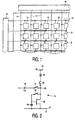
Organic electroluminescent materials offer advantages in that they are very efficient and require relatively low (DC) drive voltages. Moreover, in contrast to conventional LCDs, no backlight is required. In a simple matrix display device, the material is provided between sets of row and column address conductors at their intersections thereby forming a row and column array of electroluminescent display elements. By virtue of the diode-like I-V characteristic of the organic electroluminescent display elements, each element is capable of providing both a display and a switching function enabling multiplexed drive operation. However, when driving this simple matrix arrangement on a conventional row at a time scanning basis each display element is driven to emit light for only a small fraction of the overall field time, corresponding to a row address period. In the case of an array having N rows for example, each display element can emit light for a period equal to f/N at most where f is the field period. In order then to obtain a desired mean brightness from the display, it is necessary that the peak brightness produced by each element must be at least N times the required mean brightness and the peak display element current will be at least N times the mean current. The resulting high peak currents cause problems, notably with the more rapid degradation of the display element lifetime and with voltage drops caused along the row address conductors.
Claims (9)
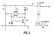
- An active matrix electroluminescent display device comprising a matrix array of electroluminescent display elements (10) each of which has an associated switching means for controlling the current through the display element in accordance with an applied current drive signal (35) and in which the switch means comprises a drive transistor (30) whose first current - carrying terminal is connected to a first potential supply line (31), whose second current - carrying terminal is connected via the display element (20) to a second potential supply line (34) and whose gate is connected to its first current - carrying terminal via a capacitance (38) characterised in that the second current - carrying terminal of the drive transistor is connected to an input terminal for inputting the current drive signal and in that a first switch device (32) is connected between the second current - carrying terminal and the gate of the transistor which is closed during the application of the current drive signal so as to store a gate voltage on the capacitance determined by the current drive signal.
- An active matrix electroluminescent display device according to Claim 1, wherein the display elements are arranged in rows and columns, and the switch devices of the switching means for a row of display elements are connected to a respective, common, row address conductor (12) via which a selection signal for closing the switch devices in that row is supplied, and each row address conductor is arranged to receive the selection signal in turn, whereby the rows of display elements are addressed one at a time in sequence.
- An active matrix electroluminescent display device according to Claim 2, wherein the drive signals for the display elements in a column are supplied via a respective column address conductor (14) common to the display elements in the column, there being a second switch device (37) connected between the input terminal of the switching means of a display element and its associated column address conductor which is closed to transfer a drive signal on the column address conductor to the input terminal when the first switch device is closed.
- An active matrix electroluminescent display device according to Claim 3, wherein the second switch device is connected to the same row address conductor as the first switch device and closed simultaneously with the first switch device by a selection signal applied to the row address conductor.
- An active matrix electroluminescent display device according to any one of Claims 2 to 4, wherein the first supply line is shared by all the display elements in the same row or column with the first supply line being provided for each row or column of display elements.
- An active matrix electroluminescent display device according to Claim 5, wherein the first supply line is associated with, and shared by, a row of display elements and comprises the row address conductor associated with a different row of display elements via which the selection signal is applied to the switch devices of the switching means of that different row.
- An active matrix electroluminescent display device accordingto any one of the preceding claims, wherein a third switch device (33) is connected between the second current - carrying terminal of the drive transistor and the display element which is opened to isolate the display element from the drive transistor when the first switch device connected between that terminal and the gate of the drive transistor is closed.
- An active matrix electroluminescent display device according to any one of Claims 1 to 6, wherein the first supply line is arranged to receive a potential pulse signal during the application of the current drive signal such as to reverse bias the display element.
- An active matrix electroluminescent display device according to any one of the preceding claims, wherein the drive transistors and the switch devices comprise thin film transistors carried on an insulating substrate.
Applications Claiming Priority (3)
| Application Number | Priority Date | Filing Date | Title |
|---|---|---|---|
| GBGB9812742.6A GB9812742D0 (en) | 1998-06-12 | 1998-06-12 | Active matrix electroluminescent display devices |
| GB9812742 | 1998-06-12 | ||
| PCT/IB1999/001041 WO1999065011A2 (en) | 1998-06-12 | 1999-06-07 | Active matrix electroluminescent display devices |
Publications (2)
| Publication Number | Publication Date |
|---|---|
| EP1034530A2 EP1034530A2 (en) | 2000-09-13 |
| EP1034530B1 true EP1034530B1 (en) | 2004-01-21 |
Family
ID=10833684
Family Applications (1)
| Application Number | Title | Priority Date | Filing Date |
|---|---|---|---|
| EP99922419A Expired - Lifetime EP1034530B1 (en) | 1998-06-12 | 1999-06-07 | Active matrix electroluminescent display devices |
Country Status (6)
| Country | Link |
|---|---|
| US (1) | US6373454B1 (en) |
| EP (1) | EP1034530B1 (en) |
| JP (1) | JP4965023B2 (en) |
| DE (1) | DE69914302T2 (en) |
| GB (1) | GB9812742D0 (en) |
| WO (1) | WO1999065011A2 (en) |
Cited By (1)
| Publication number | Priority date | Publication date | Assignee | Title |
|---|---|---|---|---|
| US8629817B2 (en) | 2006-03-10 | 2014-01-14 | Canon Kabushiki Kaisha | Driving circuit of display element and image display apparatus |
Families Citing this family (310)
| Publication number | Priority date | Publication date | Assignee | Title |
|---|---|---|---|---|
| US8115729B2 (en) | 1999-05-03 | 2012-02-14 | E Ink Corporation | Electrophoretic display element with filler particles |
| JP4079198B2 (en) * | 1999-06-17 | 2008-04-23 | ソニー株式会社 | Image display apparatus and driving method thereof |
| US7379039B2 (en) | 1999-07-14 | 2008-05-27 | Sony Corporation | Current drive circuit and display device using same pixel circuit, and drive method |
| JP4126909B2 (en) * | 1999-07-14 | 2008-07-30 | ソニー株式会社 | Current drive circuit, display device using the same, pixel circuit, and drive method |
| AU6365900A (en) * | 1999-07-21 | 2001-02-13 | E-Ink Corporation | Use of a storage capacitor to enhance the performance of an active matrix drivenelectronic display |
| JP2001109432A (en) * | 1999-10-06 | 2001-04-20 | Pioneer Electronic Corp | Driving device for active matrix type light emitting panel |
| TW587239B (en) * | 1999-11-30 | 2004-05-11 | Semiconductor Energy Lab | Electric device |
| JP4831862B2 (en) * | 1999-11-30 | 2011-12-07 | 株式会社半導体エネルギー研究所 | Electronic equipment |
| JP2001250680A (en) * | 2000-03-07 | 2001-09-14 | Pioneer Electronic Corp | Light emission element and its manufacturing method |
| JP4954380B2 (en) * | 2000-03-27 | 2012-06-13 | 株式会社半導体エネルギー研究所 | Light emitting device, semiconductor device |
| TW521226B (en) | 2000-03-27 | 2003-02-21 | Semiconductor Energy Lab | Electro-optical device |
| JP2003531487A (en) * | 2000-04-18 | 2003-10-21 | イー−インク コーポレイション | Process for manufacturing thin film transistor |
| TW521237B (en) * | 2000-04-18 | 2003-02-21 | Semiconductor Energy Lab | Light emitting device |
| US7893435B2 (en) | 2000-04-18 | 2011-02-22 | E Ink Corporation | Flexible electronic circuits and displays including a backplane comprising a patterned metal foil having a plurality of apertures extending therethrough |
| US7633471B2 (en) | 2000-05-12 | 2009-12-15 | Semiconductor Energy Laboratory Co., Ltd. | Light-emitting device and electric appliance |
| US6507156B2 (en) * | 2000-05-16 | 2003-01-14 | Planar Systems, Inc. | Display |
| TW493153B (en) * | 2000-05-22 | 2002-07-01 | Koninkl Philips Electronics Nv | Display device |
| JP3822029B2 (en) * | 2000-06-07 | 2006-09-13 | シャープ株式会社 | Light emitter, light emitting device, and display panel |
| US6738034B2 (en) | 2000-06-27 | 2004-05-18 | Hitachi, Ltd. | Picture image display device and method of driving the same |
| JP3877049B2 (en) * | 2000-06-27 | 2007-02-07 | 株式会社日立製作所 | Image display apparatus and driving method thereof |
| FR2810983B1 (en) * | 2000-06-28 | 2004-05-21 | Solvay | PROCESS FOR THE MANUFACTURE OF OXIRANNE USING A PEROXIDE COMPOUND |
| ATE470923T1 (en) * | 2000-07-07 | 2010-06-15 | Seiko Epson Corp | CURRENT SENSING CIRCUIT FOR ORGANIC ELECTROLUMINESCENCE DISPLAY |
| CN1658266A (en) | 2000-07-07 | 2005-08-24 | 精工爱普生株式会社 | Driver circuit of current driven element, and method for driving a circuit |
| AU2001280585A1 (en) * | 2000-07-18 | 2002-09-19 | Emagin Corporation | A current-type driver for organic light emitting diode displays |
| JP4925528B2 (en) * | 2000-09-29 | 2012-04-25 | 三洋電機株式会社 | Display device |
| KR100823047B1 (en) | 2000-10-02 | 2008-04-18 | 가부시키가이샤 한도오따이 에네루기 켄큐쇼 | Self light emitting device and driving method thereof |
| JP4556957B2 (en) * | 2000-10-12 | 2010-10-06 | セイコーエプソン株式会社 | Electro-optical device and electronic apparatus |
| JP3937789B2 (en) * | 2000-10-12 | 2007-06-27 | セイコーエプソン株式会社 | DRIVE CIRCUIT, ELECTRONIC DEVICE, AND ELECTRO-OPTICAL DEVICE INCLUDING ORGANIC ELECTROLUMINESCENCE ELEMENT |
| JP3594126B2 (en) * | 2000-10-13 | 2004-11-24 | 日本電気株式会社 | Current drive circuit |
| SG114502A1 (en) | 2000-10-24 | 2005-09-28 | Semiconductor Energy Lab | Light emitting device and method of driving the same |
| JP3757797B2 (en) * | 2001-01-09 | 2006-03-22 | 株式会社日立製作所 | Organic LED display and driving method thereof |
| US6912021B2 (en) * | 2001-01-22 | 2005-06-28 | Seiko Epson Corporation | Electro-optical device, method for driving electro-optical device, electronic apparatus, and method for driving electronic apparatus |
| JP2002215095A (en) * | 2001-01-22 | 2002-07-31 | Pioneer Electronic Corp | Pixel driving circuit of light emitting display |
| JP4831874B2 (en) * | 2001-02-26 | 2011-12-07 | 株式会社半導体エネルギー研究所 | LIGHT EMITTING DEVICE AND ELECTRONIC DEVICE |
| US6661180B2 (en) | 2001-03-22 | 2003-12-09 | Semiconductor Energy Laboratory Co., Ltd. | Light emitting device, driving method for the same and electronic apparatus |
| US6693385B2 (en) | 2001-03-22 | 2004-02-17 | Semiconductor Energy Laboratory Co., Ltd. | Method of driving a display device |
| AU2002309691A1 (en) * | 2001-05-09 | 2002-11-18 | Clare Micronix Integrated Systems, Inc. | Method and system for current matching in integrated circuits |
| WO2002091032A2 (en) * | 2001-05-09 | 2002-11-14 | Clare Micronix Integrated Systems, Inc. | Method and system for current balancing in visual display devices |
| US6963321B2 (en) | 2001-05-09 | 2005-11-08 | Clare Micronix Integrated Systems, Inc. | Method of providing pulse amplitude modulation for OLED display drivers |
| US7009590B2 (en) * | 2001-05-15 | 2006-03-07 | Sharp Kabushiki Kaisha | Display apparatus and display method |
| US6975304B1 (en) * | 2001-06-11 | 2005-12-13 | Handspring, Inc. | Interface for processing of an alternate symbol in a computer device |
| WO2003001496A1 (en) * | 2001-06-22 | 2003-01-03 | Ibm Corporation | Oled current drive pixel circuit |
| KR100743103B1 (en) * | 2001-06-22 | 2007-07-27 | 엘지.필립스 엘시디 주식회사 | Electro Luminescence Panel |
| JP2003005710A (en) | 2001-06-25 | 2003-01-08 | Nec Corp | Current driving circuit and image display device |
| JP4556354B2 (en) * | 2001-07-09 | 2010-10-06 | セイコーエプソン株式会社 | Drive circuit, device, and electronic device |
| JP2003043994A (en) * | 2001-07-27 | 2003-02-14 | Canon Inc | Active matrix type display |
| US6967640B2 (en) * | 2001-07-27 | 2005-11-22 | E Ink Corporation | Microencapsulated electrophoretic display with integrated driver |
| JP2003043995A (en) * | 2001-07-31 | 2003-02-14 | Matsushita Electric Ind Co Ltd | Active matrix type oled display device and its driving circuit |
| JP3951687B2 (en) * | 2001-08-02 | 2007-08-01 | セイコーエプソン株式会社 | Driving data lines used to control unit circuits |
| JP2003114646A (en) * | 2001-08-03 | 2003-04-18 | Semiconductor Energy Lab Co Ltd | Display device and its driving method |
| US6876350B2 (en) * | 2001-08-10 | 2005-04-05 | Semiconductor Energy Laboratory Co., Ltd. | Display device and electronic equipment using the same |
| US7227517B2 (en) * | 2001-08-23 | 2007-06-05 | Seiko Epson Corporation | Electronic device driving method, electronic device, semiconductor integrated circuit, and electronic apparatus |
| JP5636147B2 (en) * | 2001-08-28 | 2014-12-03 | パナソニック株式会社 | Active matrix display device |
| CN101257743B (en) | 2001-08-29 | 2011-05-25 | 株式会社半导体能源研究所 | Light emitting device, method of driving a light emitting device |
| DE60239582D1 (en) * | 2001-08-29 | 2011-05-12 | Nec Corp | Driver for a TFT display matrix |
| US7209101B2 (en) * | 2001-08-29 | 2007-04-24 | Nec Corporation | Current load device and method for driving the same |
| JP4603233B2 (en) * | 2001-08-29 | 2010-12-22 | 日本電気株式会社 | Current load element drive circuit |
| JP4650601B2 (en) * | 2001-09-05 | 2011-03-16 | 日本電気株式会社 | Current drive element drive circuit, drive method, and image display apparatus |
| US11302253B2 (en) | 2001-09-07 | 2022-04-12 | Joled Inc. | El display apparatus |
| EP3716257B1 (en) | 2001-09-07 | 2021-01-20 | Joled Inc. | El display panel, method of driving the same, and el display device |
| JP4452076B2 (en) * | 2001-09-07 | 2010-04-21 | パナソニック株式会社 | EL display device. |
| JP4581893B2 (en) * | 2001-09-10 | 2010-11-17 | セイコーエプソン株式会社 | Electronic device and electronic device |
| JP4075505B2 (en) | 2001-09-10 | 2008-04-16 | セイコーエプソン株式会社 | Electronic circuit, electronic device, and electronic apparatus |
| JP2010122700A (en) * | 2001-09-10 | 2010-06-03 | Seiko Epson Corp | Electro-optical device and electronic equipment |
| TW563088B (en) * | 2001-09-17 | 2003-11-21 | Semiconductor Energy Lab | Light emitting device, method of driving a light emitting device, and electronic equipment |
| WO2003034381A2 (en) * | 2001-09-20 | 2003-04-24 | Pioneer Corporation | Drive circuit for light emitting elements |
| SG120075A1 (en) | 2001-09-21 | 2006-03-28 | Semiconductor Energy Lab | Semiconductor device |
| CN102290005B (en) | 2001-09-21 | 2017-06-20 | 株式会社半导体能源研究所 | The driving method of organic LED display device |
| JP3810725B2 (en) | 2001-09-21 | 2006-08-16 | 株式会社半導体エネルギー研究所 | LIGHT EMITTING DEVICE AND ELECTRONIC DEVICE |
| JP2006338042A (en) * | 2001-09-21 | 2006-12-14 | Semiconductor Energy Lab Co Ltd | Light emitting device, and driving method of light emitting device |
| WO2003027998A1 (en) * | 2001-09-25 | 2003-04-03 | Matsushita Electric Industrial Co., Ltd. | El display panel and el display apparatus comprising it |
| JP5470668B2 (en) * | 2001-09-28 | 2014-04-16 | パナソニック株式会社 | Active matrix display device |
| US6777885B2 (en) * | 2001-10-12 | 2004-08-17 | Semiconductor Energy Laboratory Co., Ltd. | Drive circuit, display device using the drive circuit and electronic apparatus using the display device |
| US7365713B2 (en) | 2001-10-24 | 2008-04-29 | Semiconductor Energy Laboratory Co., Ltd. | Semiconductor device and driving method thereof |
| US7456810B2 (en) | 2001-10-26 | 2008-11-25 | Semiconductor Energy Laboratory Co., Ltd. | Light-emitting device and driving method thereof |
| US7742064B2 (en) | 2001-10-30 | 2010-06-22 | Semiconductor Energy Laboratory Co., Ltd | Signal line driver circuit, light emitting device and driving method thereof |
| US7576734B2 (en) | 2001-10-30 | 2009-08-18 | Semiconductor Energy Laboratory Co., Ltd. | Signal line driving circuit, light emitting device, and method for driving the same |
| US7180479B2 (en) | 2001-10-30 | 2007-02-20 | Semiconductor Energy Laboratory Co., Ltd. | Signal line drive circuit and light emitting device and driving method therefor |
| JP4498669B2 (en) | 2001-10-30 | 2010-07-07 | 株式会社半導体エネルギー研究所 | Semiconductor device, display device, and electronic device including the same |
| TWI261217B (en) | 2001-10-31 | 2006-09-01 | Semiconductor Energy Lab | Driving circuit of signal line and light emitting apparatus |
| US7193619B2 (en) * | 2001-10-31 | 2007-03-20 | Semiconductor Energy Laboratory Co., Ltd. | Signal line driving circuit and light emitting device |
| JP4202012B2 (en) | 2001-11-09 | 2008-12-24 | 株式会社半導体エネルギー研究所 | Light emitting device and current memory circuit |
| US7202847B2 (en) | 2002-06-28 | 2007-04-10 | E Ink Corporation | Voltage modulated driver circuits for electro-optic displays |
| US7483001B2 (en) * | 2001-11-21 | 2009-01-27 | Seiko Epson Corporation | Active matrix substrate, electro-optical device, and electronic device |
| TW529006B (en) * | 2001-11-28 | 2003-04-21 | Ind Tech Res Inst | Array circuit of light emitting diode display |
| JP2003195810A (en) | 2001-12-28 | 2003-07-09 | Casio Comput Co Ltd | Driving circuit, driving device and driving method for optical method |
| GB2384100B (en) * | 2002-01-09 | 2005-10-26 | Seiko Epson Corp | An electronic circuit for controlling the current supply to an element |
| JP2003216100A (en) * | 2002-01-21 | 2003-07-30 | Matsushita Electric Ind Co Ltd | El (electroluminescent) display panel and el display device and its driving method and method for inspecting the same device and driver circuit for the same device |
| GB0205859D0 (en) * | 2002-03-13 | 2002-04-24 | Koninkl Philips Electronics Nv | Electroluminescent display device |
| JP2004004788A (en) | 2002-04-24 | 2004-01-08 | Seiko Epson Corp | Method and circuit for controlling electron device, electronic circuit, electro-optical device, driving method for the same, and electronic equipment |
| JP3637911B2 (en) | 2002-04-24 | 2005-04-13 | セイコーエプソン株式会社 | Electronic device, electronic apparatus, and driving method of electronic device |
| CN1983365B (en) * | 2002-04-26 | 2011-05-18 | 东芝松下显示技术有限公司 | Drive circuit for electroluminescence display screen |
| WO2003092165A1 (en) | 2002-04-26 | 2003-11-06 | Toshiba Matsushita Display Technology Co., Ltd. | Semiconductor circuits for driving current-driven display and display |
| JP4357413B2 (en) * | 2002-04-26 | 2009-11-04 | 東芝モバイルディスプレイ株式会社 | EL display device |
| CN1662946A (en) | 2002-04-26 | 2005-08-31 | 东芝松下显示技术有限公司 | Drive method of EL display apparatus |
| JP2008003620A (en) * | 2002-04-26 | 2008-01-10 | Toshiba Matsushita Display Technology Co Ltd | El display device |
| US7184034B2 (en) | 2002-05-17 | 2007-02-27 | Semiconductor Energy Laboratory Co., Ltd. | Display device |
| TWI360098B (en) | 2002-05-17 | 2012-03-11 | Semiconductor Energy Lab | Display apparatus and driving method thereof |
| SG119186A1 (en) | 2002-05-17 | 2006-02-28 | Semiconductor Energy Lab | Display apparatus and driving method thereof |
| US7474285B2 (en) * | 2002-05-17 | 2009-01-06 | Semiconductor Energy Laboratory Co., Ltd. | Display apparatus and driving method thereof |
| US7170479B2 (en) | 2002-05-17 | 2007-01-30 | Semiconductor Energy Laboratory Co., Ltd. | Display device and driving method thereof |
| JP3972359B2 (en) * | 2002-06-07 | 2007-09-05 | カシオ計算機株式会社 | Display device |
| JP3918642B2 (en) | 2002-06-07 | 2007-05-23 | カシオ計算機株式会社 | Display device and driving method thereof |
| JP4610843B2 (en) * | 2002-06-20 | 2011-01-12 | カシオ計算機株式会社 | Display device and driving method of display device |
| TW594628B (en) * | 2002-07-12 | 2004-06-21 | Au Optronics Corp | Cell pixel driving circuit of OLED |
| GB0218170D0 (en) * | 2002-08-06 | 2002-09-11 | Koninkl Philips Electronics Nv | Electroluminescent display devices |
| WO2004019310A2 (en) * | 2002-08-21 | 2004-03-04 | Koninklijke Philips Electronics N.V. | Display device |
| JP4103500B2 (en) * | 2002-08-26 | 2008-06-18 | カシオ計算機株式会社 | Display device and display panel driving method |
| JP2004145278A (en) | 2002-08-30 | 2004-05-20 | Seiko Epson Corp | Electronic circuit, method for driving electronic circuit, electrooptical device, method for driving electrooptical device, and electronic apparatus |
| JP3984938B2 (en) * | 2002-09-02 | 2007-10-03 | キヤノン株式会社 | Shift register, display device, and information display device |
| JP4416456B2 (en) * | 2002-09-02 | 2010-02-17 | キヤノン株式会社 | Electroluminescence device |
| JP4350463B2 (en) * | 2002-09-02 | 2009-10-21 | キヤノン株式会社 | Input circuit, display device, and information display device |
| JP4194451B2 (en) * | 2002-09-02 | 2008-12-10 | キヤノン株式会社 | Drive circuit, display device, and information display device |
| GB0220614D0 (en) * | 2002-09-05 | 2002-10-16 | Koninkl Philips Electronics Nv | Electroluminescent display devices |
| JP2006072385A (en) * | 2002-10-03 | 2006-03-16 | Seiko Epson Corp | Electronic device and electronic equipment |
| JP2004145300A (en) | 2002-10-03 | 2004-05-20 | Seiko Epson Corp | Electronic circuit, method for driving electronic circuit, electronic device, electrooptical device, method for driving electrooptical device, and electronic apparatus |
| CN100472596C (en) | 2002-10-09 | 2009-03-25 | 三菱电机株式会社 | Constant current circuit,drive circuit and image display device |
| JP2004138773A (en) * | 2002-10-17 | 2004-05-13 | Tohoku Pioneer Corp | Active type light emission display device |
| CN100375144C (en) * | 2002-11-06 | 2008-03-12 | 三菱电机株式会社 | Sample hold circuit and image display device using the same |
| US7423617B2 (en) * | 2002-11-06 | 2008-09-09 | Tpo Displays Corp. | Light emissive element having pixel sensing circuit |
| US20050212448A1 (en) * | 2002-11-20 | 2005-09-29 | Makoto Shibusawa | Organic EL display and active matrix substrate |
| EP1571643A4 (en) * | 2002-11-20 | 2009-11-25 | Toshiba Matsushita Display Tec | Organic el display and active matrix substrate |
| US8035626B2 (en) | 2002-11-29 | 2011-10-11 | Semiconductor Energy Laboratory Co., Ltd. | Current driving circuit and display device using the current driving circuit |
| JP4566528B2 (en) | 2002-12-05 | 2010-10-20 | シャープ株式会社 | Display device |
| US7573442B2 (en) | 2002-12-06 | 2009-08-11 | Toshiba Matsushita Display Technology Co., Ltd. | Display, active matrix substrate, and driving method |
| WO2004054114A1 (en) | 2002-12-10 | 2004-06-24 | Semiconductor Energy Laboratory Co., Ltd. | Semiconductor device, digital-analog conversion circuit, and display device using them |
| CN100565637C (en) | 2002-12-27 | 2009-12-02 | 株式会社半导体能源研究所 | Semiconductor device and the display device of having used this device |
| JP4170293B2 (en) | 2003-01-17 | 2008-10-22 | 株式会社半導体エネルギー研究所 | Semiconductor device |
| JP4550372B2 (en) * | 2003-05-16 | 2010-09-22 | 東芝モバイルディスプレイ株式会社 | Active matrix display device |
| KR100732106B1 (en) | 2003-01-22 | 2007-06-27 | 도시바 마쯔시따 디스플레이 테크놀로지 컴퍼니, 리미티드 | Organic el display and active matrix substrate |
| JP4048969B2 (en) * | 2003-02-12 | 2008-02-20 | セイコーエプソン株式会社 | Electro-optical device driving method and electronic apparatus |
| JP4378087B2 (en) * | 2003-02-19 | 2009-12-02 | 奇美電子股▲ふん▼有限公司 | Image display device |
| JP3952965B2 (en) | 2003-02-25 | 2007-08-01 | カシオ計算機株式会社 | Display device and driving method of display device |
| JP4663327B2 (en) | 2003-02-28 | 2011-04-06 | 株式会社半導体エネルギー研究所 | Semiconductor device |
| JP4703103B2 (en) * | 2003-03-05 | 2011-06-15 | 東芝モバイルディスプレイ株式会社 | Driving method of active matrix type EL display device |
| TWI228696B (en) * | 2003-03-21 | 2005-03-01 | Ind Tech Res Inst | Pixel circuit for active matrix OLED and driving method |
| WO2004086344A1 (en) | 2003-03-26 | 2004-10-07 | Semiconductor Energy Laboratory Co. Ltd. | Display device and drive method thereof |
| CN102709478B (en) * | 2003-03-26 | 2016-08-17 | 株式会社半导体能源研究所 | Light-emitting device |
| JP4197287B2 (en) | 2003-03-28 | 2008-12-17 | シャープ株式会社 | Display device |
| EP1619570B1 (en) | 2003-04-25 | 2015-07-15 | Semiconductor Energy Laboratory Co., Ltd. | Semiconductor device |
| CN1820295A (en) * | 2003-05-07 | 2006-08-16 | 东芝松下显示技术有限公司 | El display and its driving method |
| KR100812846B1 (en) * | 2003-05-07 | 2008-03-11 | 도시바 마쯔시따 디스플레이 테크놀로지 컴퍼니, 리미티드 | Current output type of semiconductor device, source driver for display drive, display device, and signal input output method |
| US7453427B2 (en) | 2003-05-09 | 2008-11-18 | Semiconductor Energy Laboratory Co., Ltd. | Semiconductor device and driving method thereof |
| CN1788301A (en) * | 2003-05-13 | 2006-06-14 | 东芝松下显示技术有限公司 | Active matrix display device |
| EP2299429B1 (en) | 2003-05-14 | 2012-05-16 | Semiconductor Energy Laboratory Co., Ltd. | Semiconductor device |
| JP4467910B2 (en) * | 2003-05-16 | 2010-05-26 | 東芝モバイルディスプレイ株式会社 | Active matrix display device |
| US7566902B2 (en) | 2003-05-16 | 2009-07-28 | Semiconductor Energy Laboratory Co., Ltd. | Light-emitting device and electronic device |
| JP2004341353A (en) * | 2003-05-16 | 2004-12-02 | Toshiba Matsushita Display Technology Co Ltd | Active matrix type display device |
| JP4016962B2 (en) | 2003-05-19 | 2007-12-05 | セイコーエプソン株式会社 | Electro-optical device and driving method of electro-optical device |
| JP2004361737A (en) * | 2003-06-05 | 2004-12-24 | Nippon Hoso Kyokai <Nhk> | Organic light emitting diode driving circuit and display device using the same |
| JP2004361753A (en) * | 2003-06-05 | 2004-12-24 | Chi Mei Electronics Corp | Image display device |
| JP4727232B2 (en) | 2003-06-06 | 2011-07-20 | 株式会社半導体エネルギー研究所 | Semiconductor device |
| TW200500926A (en) * | 2003-06-17 | 2005-01-01 | Darfon Electronics Corp | Light emitting module and keyboard using the same |
| JP4662698B2 (en) * | 2003-06-25 | 2011-03-30 | ルネサスエレクトロニクス株式会社 | Current source circuit and current setting method |
| GB0315929D0 (en) * | 2003-07-08 | 2003-08-13 | Koninkl Philips Electronics Nv | Display device |
| US8378939B2 (en) | 2003-07-11 | 2013-02-19 | Semiconductor Energy Laboratory Co., Ltd. | Semiconductor device |
| US7961160B2 (en) * | 2003-07-31 | 2011-06-14 | Semiconductor Energy Laboratory Co., Ltd. | Display device, a driving method of a display device, and a semiconductor integrated circuit incorporated in a display device |
| US8085226B2 (en) | 2003-08-15 | 2011-12-27 | Semiconductor Energy Laboratory Co., Ltd. | Semiconductor device |
| WO2005027085A1 (en) | 2003-09-12 | 2005-03-24 | Semiconductor Energy Laboratory Co., Ltd. | Semiconductor device and driving method of the same |
| CA2443206A1 (en) | 2003-09-23 | 2005-03-23 | Ignis Innovation Inc. | Amoled display backplanes - pixel driver circuits, array architecture, and external compensation |
| US7193588B2 (en) * | 2003-09-29 | 2007-03-20 | Wintek Corporation | Active matrix organic electroluminescence display driving circuit |
| JP4297438B2 (en) * | 2003-11-24 | 2009-07-15 | 三星モバイルディスプレイ株式會社 | Light emitting display device, display panel, and driving method of light emitting display device |
| KR100599726B1 (en) * | 2003-11-27 | 2006-07-12 | 삼성에스디아이 주식회사 | Light emitting display device, and display panel and driving method thereof |
| JP4054794B2 (en) * | 2003-12-04 | 2008-03-05 | キヤノン株式会社 | DRIVE DEVICE, DISPLAY DEVICE, AND RECORDING DEVICE |
| JP4203656B2 (en) | 2004-01-16 | 2009-01-07 | カシオ計算機株式会社 | Display device and display panel driving method |
| JP4263153B2 (en) | 2004-01-30 | 2009-05-13 | Necエレクトロニクス株式会社 | Display device, drive circuit for display device, and semiconductor device for drive circuit |
| US7339560B2 (en) * | 2004-02-12 | 2008-03-04 | Au Optronics Corporation | OLED pixel |
| US7173585B2 (en) | 2004-03-10 | 2007-02-06 | Wintek Corporation | Active matrix display driving circuit |
| JP2005275315A (en) * | 2004-03-26 | 2005-10-06 | Semiconductor Energy Lab Co Ltd | Display device, driving method therefor, and electronic equipment using the same |
| JP4665419B2 (en) | 2004-03-30 | 2011-04-06 | カシオ計算機株式会社 | Pixel circuit board inspection method and inspection apparatus |
| US20050224197A1 (en) * | 2004-04-12 | 2005-10-13 | Cheng Wen P | Combining device for tightly fixing screen to wall |
| US6977470B2 (en) * | 2004-04-28 | 2005-12-20 | Au Optronics Corp. | Current-driven OLED pixel |
| TWI288900B (en) | 2004-04-30 | 2007-10-21 | Fujifilm Corp | Active matrix type display device |
| US20050258867A1 (en) * | 2004-05-21 | 2005-11-24 | Seiko Epson Corporation | Electronic circuit, electro-optical device, electronic device and electronic apparatus |
| US8355015B2 (en) | 2004-05-21 | 2013-01-15 | Semiconductor Energy Laboratory Co., Ltd. | Semiconductor device, display device and electronic device including a diode electrically connected to a signal line |
| JP2005352063A (en) | 2004-06-09 | 2005-12-22 | Mitsubishi Electric Corp | Image display apparatus |
| US20050275352A1 (en) * | 2004-06-14 | 2005-12-15 | Au Optronics Corporation. | Redundant storage capacitor and method for repairing OLED pixels and driving circuits |
| US7608861B2 (en) | 2004-06-24 | 2009-10-27 | Canon Kabushiki Kaisha | Active matrix type display having two transistors of opposite conductivity acting as a single switch for the driving transistor of a display element |
| EP1610292B1 (en) | 2004-06-25 | 2016-06-15 | Semiconductor Energy Laboratory Co., Ltd. | Display device, driving method thereof and electronic device |
| CA2472671A1 (en) | 2004-06-29 | 2005-12-29 | Ignis Innovation Inc. | Voltage-programming scheme for current-driven amoled displays |
| TWI280534B (en) * | 2004-09-14 | 2007-05-01 | Toshiba Matsushita Display Tec | Display, array substrate, and display manufacturing method |
| JP4192133B2 (en) * | 2004-09-28 | 2008-12-03 | 東芝松下ディスプレイテクノロジー株式会社 | Display device and driving method thereof |
| JP4501785B2 (en) | 2004-09-30 | 2010-07-14 | セイコーエプソン株式会社 | Pixel circuit and electronic device |
| KR100602352B1 (en) * | 2004-11-22 | 2006-07-18 | 삼성에스디아이 주식회사 | Pixel and Light Emitting Display Using The Same |
| JP4438066B2 (en) * | 2004-11-26 | 2010-03-24 | キヤノン株式会社 | Active matrix display device and current programming method thereof |
| US7502040B2 (en) * | 2004-12-06 | 2009-03-10 | Semiconductor Energy Laboratory Co., Ltd. | Display device, driving method thereof and electronic appliance |
| US9171500B2 (en) | 2011-05-20 | 2015-10-27 | Ignis Innovation Inc. | System and methods for extraction of parasitic parameters in AMOLED displays |
| US8576217B2 (en) | 2011-05-20 | 2013-11-05 | Ignis Innovation Inc. | System and methods for extraction of threshold and mobility parameters in AMOLED displays |
| US10012678B2 (en) | 2004-12-15 | 2018-07-03 | Ignis Innovation Inc. | Method and system for programming, calibrating and/or compensating, and driving an LED display |
| US10013907B2 (en) | 2004-12-15 | 2018-07-03 | Ignis Innovation Inc. | Method and system for programming, calibrating and/or compensating, and driving an LED display |
| US20140111567A1 (en) | 2005-04-12 | 2014-04-24 | Ignis Innovation Inc. | System and method for compensation of non-uniformities in light emitting device displays |
| US9280933B2 (en) | 2004-12-15 | 2016-03-08 | Ignis Innovation Inc. | System and methods for extraction of threshold and mobility parameters in AMOLED displays |
| US9799246B2 (en) | 2011-05-20 | 2017-10-24 | Ignis Innovation Inc. | System and methods for extraction of threshold and mobility parameters in AMOLED displays |
| US9275579B2 (en) | 2004-12-15 | 2016-03-01 | Ignis Innovation Inc. | System and methods for extraction of threshold and mobility parameters in AMOLED displays |
| US8599191B2 (en) | 2011-05-20 | 2013-12-03 | Ignis Innovation Inc. | System and methods for extraction of threshold and mobility parameters in AMOLED displays |
| JP5128287B2 (en) | 2004-12-15 | 2013-01-23 | イグニス・イノベイション・インコーポレーテッド | Method and system for performing real-time calibration for display arrays |
| JP2006184576A (en) * | 2004-12-27 | 2006-07-13 | Toshiba Matsushita Display Technology Co Ltd | Luminous type display device and array substrate |
| JP2006184577A (en) * | 2004-12-27 | 2006-07-13 | Toshiba Matsushita Display Technology Co Ltd | Display device, array substrate, and method of manufacturing display device |
| US20060139265A1 (en) * | 2004-12-28 | 2006-06-29 | Semiconductor Energy Laboratory Co., Ltd. | Driving method of display device |
| US20060158399A1 (en) | 2005-01-14 | 2006-07-20 | Semiconductor Energy Laboratory Co., Ltd. | Driving method of display device |
| JP4987310B2 (en) * | 2005-01-31 | 2012-07-25 | 株式会社ジャパンディスプレイセントラル | Display device, array substrate, and driving method of display device |
| US7746299B2 (en) * | 2005-01-31 | 2010-06-29 | Toshiba Matsushita Display Technology Co., Ltd. | Display, array substrate, and method of driving display |
| CA2496642A1 (en) | 2005-02-10 | 2006-08-10 | Ignis Innovation Inc. | Fast settling time driving method for organic light-emitting diode (oled) displays based on current programming |
| EP1854088A4 (en) * | 2005-02-28 | 2009-12-09 | Toshiba Matsushita Display Tec | Display and method of manufacturing the same |
| JP2006251049A (en) * | 2005-03-08 | 2006-09-21 | Toshiba Matsushita Display Technology Co Ltd | Display apparatus and array substrate |
| US20060221005A1 (en) * | 2005-03-31 | 2006-10-05 | Kazuyoshi Omata | Display, array substrate, and method of driving display |
| US7355220B2 (en) * | 2005-03-31 | 2008-04-08 | Toshiba Matsushita Display Technology Co., Ltd. | Array substrate |
| JP2006309110A (en) * | 2005-03-31 | 2006-11-09 | Toshiba Matsushita Display Technology Co Ltd | Display, array substrate, and method of manufacturing display |
| JP2006284916A (en) * | 2005-03-31 | 2006-10-19 | Toshiba Matsushita Display Technology Co Ltd | Display device, array substrate, and method of driving display device |
| JP2006284914A (en) * | 2005-03-31 | 2006-10-19 | Toshiba Matsushita Display Technology Co Ltd | Display device and driving method therefor |
| JP2006284945A (en) * | 2005-03-31 | 2006-10-19 | Toshiba Matsushita Display Technology Co Ltd | Display device and driving method therefor |
| JP2006284944A (en) * | 2005-03-31 | 2006-10-19 | Toshiba Matsushita Display Technology Co Ltd | Display device, array substrate, and driving method of display device |
| US7719526B2 (en) | 2005-04-14 | 2010-05-18 | Semiconductor Energy Laboratory Co., Ltd. | Display device, and driving method and electronic apparatus of the display device |
| US8633919B2 (en) * | 2005-04-14 | 2014-01-21 | Semiconductor Energy Laboratory Co., Ltd. | Display device, driving method of the display device, and electronic device |
| EP1720148A3 (en) | 2005-05-02 | 2007-09-05 | Semiconductor Energy Laboratory Co., Ltd. | Display device and gray scale driving method with subframes thereof |
| US7852298B2 (en) | 2005-06-08 | 2010-12-14 | Ignis Innovation Inc. | Method and system for driving a light emitting device display |
| JP2007003792A (en) * | 2005-06-23 | 2007-01-11 | Toshiba Matsushita Display Technology Co Ltd | Display apparatus and array substrate |
| TW200707385A (en) * | 2005-07-15 | 2007-02-16 | Seiko Epson Corp | Electronic device, method of driving the same, electro-optical device, and electronic apparatus |
| JP4826158B2 (en) * | 2005-07-25 | 2011-11-30 | セイコーエプソン株式会社 | Electro-optic device |
| TWI485681B (en) * | 2005-08-12 | 2015-05-21 | Semiconductor Energy Lab | Display device |
| CA2518276A1 (en) | 2005-09-13 | 2007-03-13 | Ignis Innovation Inc. | Compensation technique for luminance degradation in electro-luminance devices |
| EP1764770A3 (en) * | 2005-09-16 | 2012-03-14 | Semiconductor Energy Laboratory Co., Ltd. | Display device and driving method of display device |
| JP4556814B2 (en) * | 2005-09-16 | 2010-10-06 | セイコーエプソン株式会社 | Device, device driving method, and electronic apparatus |
| JP2006072377A (en) * | 2005-09-16 | 2006-03-16 | Seiko Epson Corp | Circuit, device, and electronic equipment |
| JP2007133351A (en) * | 2005-10-12 | 2007-05-31 | Canon Inc | Display unit, active matrix device, and driving method thereof |
| EP1777690B1 (en) | 2005-10-18 | 2012-08-01 | Semiconductor Energy Laboratory Co., Ltd. | Display device |
| JP4991138B2 (en) * | 2005-10-20 | 2012-08-01 | 株式会社ジャパンディスプレイセントラル | Driving method and driving apparatus for active matrix display device |
| JP2007121629A (en) * | 2005-10-27 | 2007-05-17 | Canon Inc | Active matrix type display device and camera |
| US20070126667A1 (en) * | 2005-12-01 | 2007-06-07 | Toshiba Matsushita Display Technology Co., Ltd. | El display apparatus and method for driving el display apparatus |
| EP1793367A3 (en) | 2005-12-02 | 2009-08-26 | Semiconductor Energy Laboratory Co., Ltd. | Semiconductor device |
| KR101404582B1 (en) * | 2006-01-20 | 2014-06-09 | 가부시키가이샤 한도오따이 에네루기 켄큐쇼 | Driving method of display device |
| KR100965022B1 (en) * | 2006-02-20 | 2010-06-21 | 도시바 모바일 디스플레이 가부시키가이샤 | El display apparatus and method for driving el display apparatus |
| TWI279763B (en) * | 2006-03-13 | 2007-04-21 | Himax Tech Ltd | Light emitting display, pixel circuit and driving method thereof |
| JP5224702B2 (en) | 2006-03-13 | 2013-07-03 | キヤノン株式会社 | Pixel circuit and image display device having the pixel circuit |
| US7616179B2 (en) * | 2006-03-31 | 2009-11-10 | Canon Kabushiki Kaisha | Organic EL display apparatus and driving method therefor |
| KR100784014B1 (en) * | 2006-04-17 | 2007-12-07 | 삼성에스디아이 주식회사 | Organic Light Emitting Display Device and Driving Method Thereof |
| WO2007118332A1 (en) | 2006-04-19 | 2007-10-25 | Ignis Innovation Inc. | Stable driving scheme for active matrix displays |
| JP4208902B2 (en) * | 2006-06-30 | 2009-01-14 | キヤノン株式会社 | Active matrix display device and driving method thereof |
| JP5196744B2 (en) * | 2006-06-30 | 2013-05-15 | キヤノン株式会社 | Active matrix display device |
| JP4208903B2 (en) * | 2006-06-30 | 2009-01-14 | キヤノン株式会社 | Active matrix display device and information processing device using the same |
| CA2556961A1 (en) | 2006-08-15 | 2008-02-15 | Ignis Innovation Inc. | Oled compensation technique based on oled capacitance |
| WO2008029717A1 (en) * | 2006-09-05 | 2008-03-13 | Canon Kabushiki Kaisha | Organic light emitting display device |
| JP5665256B2 (en) * | 2006-12-20 | 2015-02-04 | キヤノン株式会社 | Luminescent display device |
| US7355574B1 (en) * | 2007-01-24 | 2008-04-08 | Eastman Kodak Company | OLED display with aging and efficiency compensation |
| JP5361139B2 (en) * | 2007-03-09 | 2013-12-04 | キヤノン株式会社 | Display device |
| JP2008298970A (en) * | 2007-05-30 | 2008-12-11 | Canon Inc | Organic el pixel circuit and its driving method |
| JP2009104104A (en) * | 2007-05-30 | 2009-05-14 | Canon Inc | Active matrix display and its driving method |
| JP4969322B2 (en) * | 2007-06-01 | 2012-07-04 | 三菱電機株式会社 | Voltage generating circuit and image display device including the same |
| JP5495510B2 (en) * | 2007-06-19 | 2014-05-21 | キヤノン株式会社 | Display device and electronic apparatus using the same |
| US20090006198A1 (en) * | 2007-06-29 | 2009-01-01 | David George Walsh | Product displays for retail stores |
| JP2009014836A (en) * | 2007-07-02 | 2009-01-22 | Canon Inc | Active matrix type display and driving method therefor |
| JP2009037123A (en) * | 2007-08-03 | 2009-02-19 | Canon Inc | Active matrix display device and its driving method |
| CN101779229B (en) * | 2007-08-21 | 2012-11-07 | 佳能株式会社 | Display apparatus and drive method thereof |
| US20090066615A1 (en) * | 2007-09-11 | 2009-03-12 | Canon Kabushiki Kaisha | Display apparatus and driving method thereof |
| JP2009080272A (en) * | 2007-09-26 | 2009-04-16 | Canon Inc | Active matrix type display device |
| JP2009109641A (en) * | 2007-10-29 | 2009-05-21 | Canon Inc | Driving circuit and active matrix type display device |
| JP2008146051A (en) * | 2007-11-22 | 2008-06-26 | Toshiba Matsushita Display Technology Co Ltd | El display device |
| EP2227512A1 (en) * | 2007-12-18 | 2010-09-15 | Lumimove, Inc., Dba Crosslink | Flexible electroluminescent devices and systems |
| JP2009265410A (en) * | 2008-04-25 | 2009-11-12 | Toshiba Mobile Display Co Ltd | Active matrix type display apparatus |
| JP2010008987A (en) * | 2008-06-30 | 2010-01-14 | Canon Inc | Drive circuit |
| CA2688870A1 (en) | 2009-11-30 | 2011-05-30 | Ignis Innovation Inc. | Methode and techniques for improving display uniformity |
| US9311859B2 (en) | 2009-11-30 | 2016-04-12 | Ignis Innovation Inc. | Resetting cycle for aging compensation in AMOLED displays |
| US10319307B2 (en) | 2009-06-16 | 2019-06-11 | Ignis Innovation Inc. | Display system with compensation techniques and/or shared level resources |
| US9384698B2 (en) | 2009-11-30 | 2016-07-05 | Ignis Innovation Inc. | System and methods for aging compensation in AMOLED displays |
| CA2669367A1 (en) | 2009-06-16 | 2010-12-16 | Ignis Innovation Inc | Compensation technique for color shift in displays |
| JP5284198B2 (en) * | 2009-06-30 | 2013-09-11 | キヤノン株式会社 | Display device and driving method thereof |
| JP2011013415A (en) * | 2009-07-01 | 2011-01-20 | Canon Inc | Active matrix type display apparatus |
| US8786526B2 (en) | 2009-07-28 | 2014-07-22 | Sharp Kabushiki Kaisha | Active matrix substrate, display device, and organic EL display device |
| JP2011028135A (en) * | 2009-07-29 | 2011-02-10 | Canon Inc | Display device and driving method of the same |
| US10996258B2 (en) | 2009-11-30 | 2021-05-04 | Ignis Innovation Inc. | Defect detection and correction of pixel circuits for AMOLED displays |
| US8803417B2 (en) | 2009-12-01 | 2014-08-12 | Ignis Innovation Inc. | High resolution pixel architecture |
| CA2687631A1 (en) | 2009-12-06 | 2011-06-06 | Ignis Innovation Inc | Low power driving scheme for display applications |
| JP2010134471A (en) * | 2010-01-12 | 2010-06-17 | Hitachi Displays Ltd | Image display apparatus |
| US10089921B2 (en) | 2010-02-04 | 2018-10-02 | Ignis Innovation Inc. | System and methods for extracting correlation curves for an organic light emitting device |
| US9881532B2 (en) | 2010-02-04 | 2018-01-30 | Ignis Innovation Inc. | System and method for extracting correlation curves for an organic light emitting device |
| US20140313111A1 (en) | 2010-02-04 | 2014-10-23 | Ignis Innovation Inc. | System and methods for extracting correlation curves for an organic light emitting device |
| CA2692097A1 (en) | 2010-02-04 | 2011-08-04 | Ignis Innovation Inc. | Extracting correlation curves for light emitting device |
| US10163401B2 (en) | 2010-02-04 | 2018-12-25 | Ignis Innovation Inc. | System and methods for extracting correlation curves for an organic light emitting device |
| US10176736B2 (en) | 2010-02-04 | 2019-01-08 | Ignis Innovation Inc. | System and methods for extracting correlation curves for an organic light emitting device |
| CA2696778A1 (en) | 2010-03-17 | 2011-09-17 | Ignis Innovation Inc. | Lifetime, uniformity, parameter extraction methods |
| US8513897B2 (en) * | 2010-10-01 | 2013-08-20 | Winstar Display Co., Ltd | OLED display with a current stabilizing device and its driving method |
| US8907991B2 (en) | 2010-12-02 | 2014-12-09 | Ignis Innovation Inc. | System and methods for thermal compensation in AMOLED displays |
| US9530349B2 (en) | 2011-05-20 | 2016-12-27 | Ignis Innovations Inc. | Charged-based compensation and parameter extraction in AMOLED displays |
| US9466240B2 (en) | 2011-05-26 | 2016-10-11 | Ignis Innovation Inc. | Adaptive feedback system for compensating for aging pixel areas with enhanced estimation speed |
| CN106910464B (en) | 2011-05-27 | 2020-04-24 | 伊格尼斯创新公司 | System for compensating pixels in a display array and pixel circuit for driving light emitting devices |
| US10089924B2 (en) | 2011-11-29 | 2018-10-02 | Ignis Innovation Inc. | Structural and low-frequency non-uniformity compensation |
| US9324268B2 (en) | 2013-03-15 | 2016-04-26 | Ignis Innovation Inc. | Amoled displays with multiple readout circuits |
| JP6124573B2 (en) | 2011-12-20 | 2017-05-10 | キヤノン株式会社 | Display device |
| US8937632B2 (en) | 2012-02-03 | 2015-01-20 | Ignis Innovation Inc. | Driving system for active-matrix displays |
| US9747834B2 (en) | 2012-05-11 | 2017-08-29 | Ignis Innovation Inc. | Pixel circuits including feedback capacitors and reset capacitors, and display systems therefore |
| US8922544B2 (en) | 2012-05-23 | 2014-12-30 | Ignis Innovation Inc. | Display systems with compensation for line propagation delay |
| US9786223B2 (en) | 2012-12-11 | 2017-10-10 | Ignis Innovation Inc. | Pixel circuits for AMOLED displays |
| US9336717B2 (en) | 2012-12-11 | 2016-05-10 | Ignis Innovation Inc. | Pixel circuits for AMOLED displays |
| US9830857B2 (en) | 2013-01-14 | 2017-11-28 | Ignis Innovation Inc. | Cleaning common unwanted signals from pixel measurements in emissive displays |
| WO2014108879A1 (en) | 2013-01-14 | 2014-07-17 | Ignis Innovation Inc. | Driving scheme for emissive displays providing compensation for driving transistor variations |
| EP3043338A1 (en) | 2013-03-14 | 2016-07-13 | Ignis Innovation Inc. | Re-interpolation with edge detection for extracting an aging pattern for amoled displays |
| WO2014174427A1 (en) | 2013-04-22 | 2014-10-30 | Ignis Innovation Inc. | Inspection system for oled display panels |
| DE112014003719T5 (en) | 2013-08-12 | 2016-05-19 | Ignis Innovation Inc. | compensation accuracy |
| US9083320B2 (en) | 2013-09-20 | 2015-07-14 | Maofeng YANG | Apparatus and method for electrical stability compensation |
| US9741282B2 (en) | 2013-12-06 | 2017-08-22 | Ignis Innovation Inc. | OLED display system and method |
| US9761170B2 (en) | 2013-12-06 | 2017-09-12 | Ignis Innovation Inc. | Correction for localized phenomena in an image array |
| US9806098B2 (en) | 2013-12-10 | 2017-10-31 | Semiconductor Energy Laboratory Co., Ltd. | Light-emitting device |
| US9502653B2 (en) | 2013-12-25 | 2016-11-22 | Ignis Innovation Inc. | Electrode contacts |
| DE102015206281A1 (en) | 2014-04-08 | 2015-10-08 | Ignis Innovation Inc. | Display system with shared level resources for portable devices |
| JP5752295B2 (en) * | 2014-05-29 | 2015-07-22 | 株式会社半導体エネルギー研究所 | Display device |
| CA2879462A1 (en) | 2015-01-23 | 2016-07-23 | Ignis Innovation Inc. | Compensation for color variation in emissive devices |
| CA2889870A1 (en) | 2015-05-04 | 2016-11-04 | Ignis Innovation Inc. | Optical feedback system |
| CA2892714A1 (en) | 2015-05-27 | 2016-11-27 | Ignis Innovation Inc | Memory bandwidth reduction in compensation system |
| CA2900170A1 (en) | 2015-08-07 | 2017-02-07 | Gholamreza Chaji | Calibration of pixel based on improved reference values |
| CN105489165B (en) | 2016-01-29 | 2018-05-11 | 深圳市华星光电技术有限公司 | Pixel compensation circuit, method, scan drive circuit and flat display apparatus |
Family Cites Families (15)
| Publication number | Priority date | Publication date | Assignee | Title |
|---|---|---|---|---|
| JPH0542488Y2 (en) * | 1986-01-28 | 1993-10-26 | ||
| US4967140A (en) * | 1988-09-12 | 1990-10-30 | U.S. Philips Corporation | Current-source arrangement |
| US4996523A (en) * | 1988-10-20 | 1991-02-26 | Eastman Kodak Company | Electroluminescent storage display with improved intensity driver circuits |
| JPH04161984A (en) * | 1990-10-26 | 1992-06-05 | Opt Tec Corp | Large-sized picture display board system having multiple gray level |
| US5302966A (en) * | 1992-06-02 | 1994-04-12 | David Sarnoff Research Center, Inc. | Active matrix electroluminescent display and method of operation |
| GB9301463D0 (en) * | 1993-01-26 | 1993-03-17 | Philips Electronics Uk Ltd | Current memory |
| JP2821347B2 (en) * | 1993-10-12 | 1998-11-05 | 日本電気株式会社 | Current control type light emitting element array |
| JP2689916B2 (en) * | 1994-08-09 | 1997-12-10 | 日本電気株式会社 | Active matrix type current control type light emitting element drive circuit |
| US5652600A (en) * | 1994-11-17 | 1997-07-29 | Planar Systems, Inc. | Time multiplexed gray scale approach |
| US5684365A (en) * | 1994-12-14 | 1997-11-04 | Eastman Kodak Company | TFT-el display panel using organic electroluminescent media |
| WO1996036959A2 (en) | 1995-05-19 | 1996-11-21 | Philips Electronics N.V. | Display device |
| KR20050084509A (en) * | 1997-04-23 | 2005-08-26 | 사르노프 코포레이션 | Active matrix light emitting diode pixel structure and method |
| US6229506B1 (en) * | 1997-04-23 | 2001-05-08 | Sarnoff Corporation | Active matrix light emitting diode pixel structure and concomitant method |
| US6034659A (en) * | 1998-02-02 | 2000-03-07 | Wald; Steven F. | Active matrix electroluminescent grey scale display |
| JP3252897B2 (en) * | 1998-03-31 | 2002-02-04 | 日本電気株式会社 | Element driving device and method, image display device |
-
1998
- 1998-06-12 GB GBGB9812742.6A patent/GB9812742D0/en not_active Ceased
-
1999
- 1999-06-07 WO PCT/IB1999/001041 patent/WO1999065011A2/en active IP Right Grant
- 1999-06-07 JP JP2000553938A patent/JP4965023B2/en not_active Expired - Lifetime
- 1999-06-07 EP EP99922419A patent/EP1034530B1/en not_active Expired - Lifetime
- 1999-06-07 DE DE1999614302 patent/DE69914302T2/en not_active Expired - Lifetime
- 1999-06-09 US US09/329,027 patent/US6373454B1/en not_active Expired - Lifetime
Cited By (1)
| Publication number | Priority date | Publication date | Assignee | Title |
|---|---|---|---|---|
| US8629817B2 (en) | 2006-03-10 | 2014-01-14 | Canon Kabushiki Kaisha | Driving circuit of display element and image display apparatus |
Also Published As
| Publication number | Publication date |
|---|---|
| US6373454B1 (en) | 2002-04-16 |
| EP1034530A2 (en) | 2000-09-13 |
| DE69914302T2 (en) | 2004-11-18 |
| JP4965023B2 (en) | 2012-07-04 |
| DE69914302D1 (en) | 2004-02-26 |
| GB9812742D0 (en) | 1998-08-12 |
| JP2002517806A (en) | 2002-06-18 |
| WO1999065011A2 (en) | 1999-12-16 |
| WO1999065011A3 (en) | 2000-03-09 |
Similar Documents
| Publication | Publication Date | Title |
|---|---|---|
| EP1034530B1 (en) | Active matrix electroluminescent display devices | |
| EP1034529B1 (en) | Active matrix electroluminescent display devices | |
| US7221342B2 (en) | Electroluminescent display device | |
| US6498438B1 (en) | Current source and display device using the same | |
| US7619593B2 (en) | Active matrix display device | |
| DE102006057537B4 (en) | OLED display device and driving method | |
| US7564433B2 (en) | Active matrix display devices | |
| KR100593276B1 (en) | Oled current drive pixel circuit | |
| EP1704554B1 (en) | Electroluminescent display devices with an active matrix | |
| US20060022204A1 (en) | Electroluminescent display devices | |
| KR20070000422A (en) | Threshold voltage compensation method for electroluminescent display devices | |
| KR20060136392A (en) | Threshold voltage compensation method for electroluminescent display devices | |
| EP1459284A1 (en) | Active matrix electroluminescent display device | |
| US20030117347A1 (en) | Active matrix electroluminescent display device |
Legal Events
| Date | Code | Title | Description |
|---|---|---|---|
| PUAI | Public reference made under article 153(3) epc to a published international application that has entered the european phase |
Free format text: ORIGINAL CODE: 0009012 |
|
| 17P | Request for examination filed |
Effective date: 20000313 |
|
| AK | Designated contracting states |
Kind code of ref document: A2 Designated state(s): DE FR GB NL |
|
| GRAH | Despatch of communication of intention to grant a patent |
Free format text: ORIGINAL CODE: EPIDOS IGRA |
|
| GRAS | Grant fee paid |
Free format text: ORIGINAL CODE: EPIDOSNIGR3 |
|
| GRAA | (expected) grant |
Free format text: ORIGINAL CODE: 0009210 |
|
| AK | Designated contracting states |
Kind code of ref document: B1 Designated state(s): DE FR GB NL |
|
| PG25 | Lapsed in a contracting state [announced via postgrant information from national office to epo] |
Ref country code: NL Free format text: LAPSE BECAUSE OF FAILURE TO SUBMIT A TRANSLATION OF THE DESCRIPTION OR TO PAY THE FEE WITHIN THE PRESCRIBED TIME-LIMIT Effective date: 20040121 |
|
| REG | Reference to a national code |
Ref country code: GB Ref legal event code: FG4D |
|
| REG | Reference to a national code |
Ref country code: GB Ref legal event code: 746 Effective date: 20040202 |
|
| REF | Corresponds to: |
Ref document number: 69914302 Country of ref document: DE Date of ref document: 20040226 Kind code of ref document: P |
|
| NLV1 | Nl: lapsed or annulled due to failure to fulfill the requirements of art. 29p and 29m of the patents act | ||
| ET | Fr: translation filed | ||
| REG | Reference to a national code |
Ref country code: FR Ref legal event code: D6 |
|
| PLBE | No opposition filed within time limit |
Free format text: ORIGINAL CODE: 0009261 |
|
| STAA | Information on the status of an ep patent application or granted ep patent |
Free format text: STATUS: NO OPPOSITION FILED WITHIN TIME LIMIT |
|
| 26N | No opposition filed |
Effective date: 20041022 |
|
| REG | Reference to a national code |
Ref country code: DE Ref legal event code: R081 Ref document number: 69914302 Country of ref document: DE Owner name: KONINKLIJKE PHILIPS N.V., NL Free format text: FORMER OWNER: KONINKLIJKE PHILIPS ELECTRONICS N.V., EINDHOVEN, NL Effective date: 20140328 |
|
| REG | Reference to a national code |
Ref country code: FR Ref legal event code: CD Owner name: KONINKLIJKE PHILIPS N.V., NL Effective date: 20141126 Ref country code: FR Ref legal event code: CA Effective date: 20141126 |
|
| REG | Reference to a national code |
Ref country code: FR Ref legal event code: PLFP Year of fee payment: 18 |
|
| REG | Reference to a national code |
Ref country code: FR Ref legal event code: PLFP Year of fee payment: 19 |
|
| REG | Reference to a national code |
Ref country code: DE Ref legal event code: R082 Ref document number: 69914302 Country of ref document: DE Representative=s name: DOMPATENT VON KREISLER SELTING WERNER - PARTNE, DE |
|
| REG | Reference to a national code |
Ref country code: FR Ref legal event code: PLFP Year of fee payment: 20 |
|
| PGFP | Annual fee paid to national office [announced via postgrant information from national office to epo] |
Ref country code: FR Payment date: 20180620 Year of fee payment: 20 |
|
| REG | Reference to a national code |
Ref country code: GB Ref legal event code: 732E Free format text: REGISTERED BETWEEN 20180809 AND 20180815 |
|
| PGFP | Annual fee paid to national office [announced via postgrant information from national office to epo] |
Ref country code: GB Payment date: 20180620 Year of fee payment: 20 Ref country code: DE Payment date: 20180625 Year of fee payment: 20 |
|
| REG | Reference to a national code |
Ref country code: DE Ref legal event code: R071 Ref document number: 69914302 Country of ref document: DE |
|
| REG | Reference to a national code |
Ref country code: GB Ref legal event code: PE20 Expiry date: 20190606 |
|
| REG | Reference to a national code |
Ref country code: DE Ref legal event code: R082 Ref document number: 69914302 Country of ref document: DE Representative=s name: DOMPATENT VON KREISLER SELTING WERNER - PARTNE, DE Ref country code: DE Ref legal event code: R081 Ref document number: 69914302 Country of ref document: DE Owner name: BEIJING XIAOMI MOBILE SOFTWARE CO., LTD., CN Free format text: FORMER OWNER: KONINKLIJKE PHILIPS N.V., EINDHOVEN, NL |
|
| PG25 | Lapsed in a contracting state [announced via postgrant information from national office to epo] |
Ref country code: GB Free format text: LAPSE BECAUSE OF EXPIRATION OF PROTECTION Effective date: 20190606 |