EP1041624A1 - Method of transferring ultra-thin substrates and application of the method to the manufacture of a multilayer thin film device - Google Patents
Method of transferring ultra-thin substrates and application of the method to the manufacture of a multilayer thin film device Download PDFInfo
- Publication number
- EP1041624A1 EP1041624A1 EP99201061A EP99201061A EP1041624A1 EP 1041624 A1 EP1041624 A1 EP 1041624A1 EP 99201061 A EP99201061 A EP 99201061A EP 99201061 A EP99201061 A EP 99201061A EP 1041624 A1 EP1041624 A1 EP 1041624A1
- Authority
- EP
- European Patent Office
- Prior art keywords
- substrate
- layer
- planar
- semiconductor device
- attaching
- Prior art date
- Legal status (The legal status is an assumption and is not a legal conclusion. Google has not performed a legal analysis and makes no representation as to the accuracy of the status listed.)
- Withdrawn
Links
Images


Classifications
-
- H—ELECTRICITY
- H01—ELECTRIC ELEMENTS
- H01L—SEMICONDUCTOR DEVICES NOT COVERED BY CLASS H10
- H01L25/00—Assemblies consisting of a plurality of individual semiconductor or other solid state devices ; Multistep manufacturing processes thereof
- H01L25/50—Multistep manufacturing processes of assemblies consisting of devices, each device being of a type provided for in group H01L27/00 or H01L29/00
-
- H—ELECTRICITY
- H01—ELECTRIC ELEMENTS
- H01L—SEMICONDUCTOR DEVICES NOT COVERED BY CLASS H10
- H01L21/00—Processes or apparatus adapted for the manufacture or treatment of semiconductor or solid state devices or of parts thereof
- H01L21/67—Apparatus specially adapted for handling semiconductor or electric solid state devices during manufacture or treatment thereof; Apparatus specially adapted for handling wafers during manufacture or treatment of semiconductor or electric solid state devices or components ; Apparatus not specifically provided for elsewhere
- H01L21/683—Apparatus specially adapted for handling semiconductor or electric solid state devices during manufacture or treatment thereof; Apparatus specially adapted for handling wafers during manufacture or treatment of semiconductor or electric solid state devices or components ; Apparatus not specifically provided for elsewhere for supporting or gripping
- H01L21/6835—Apparatus specially adapted for handling semiconductor or electric solid state devices during manufacture or treatment thereof; Apparatus specially adapted for handling wafers during manufacture or treatment of semiconductor or electric solid state devices or components ; Apparatus not specifically provided for elsewhere for supporting or gripping using temporarily an auxiliary support
-
- H—ELECTRICITY
- H01—ELECTRIC ELEMENTS
- H01L—SEMICONDUCTOR DEVICES NOT COVERED BY CLASS H10
- H01L23/00—Details of semiconductor or other solid state devices
- H01L23/52—Arrangements for conducting electric current within the device in operation from one component to another, i.e. interconnections, e.g. wires, lead frames
- H01L23/538—Arrangements for conducting electric current within the device in operation from one component to another, i.e. interconnections, e.g. wires, lead frames the interconnection structure between a plurality of semiconductor chips being formed on, or in, insulating substrates
- H01L23/5385—Assembly of a plurality of insulating substrates
-
- H—ELECTRICITY
- H01—ELECTRIC ELEMENTS
- H01L—SEMICONDUCTOR DEVICES NOT COVERED BY CLASS H10
- H01L23/00—Details of semiconductor or other solid state devices
- H01L23/52—Arrangements for conducting electric current within the device in operation from one component to another, i.e. interconnections, e.g. wires, lead frames
- H01L23/538—Arrangements for conducting electric current within the device in operation from one component to another, i.e. interconnections, e.g. wires, lead frames the interconnection structure between a plurality of semiconductor chips being formed on, or in, insulating substrates
- H01L23/5389—Arrangements for conducting electric current within the device in operation from one component to another, i.e. interconnections, e.g. wires, lead frames the interconnection structure between a plurality of semiconductor chips being formed on, or in, insulating substrates the chips being integrally enclosed by the interconnect and support structures
-
- H—ELECTRICITY
- H01—ELECTRIC ELEMENTS
- H01L—SEMICONDUCTOR DEVICES NOT COVERED BY CLASS H10
- H01L24/00—Arrangements for connecting or disconnecting semiconductor or solid-state bodies; Methods or apparatus related thereto
- H01L24/01—Means for bonding being attached to, or being formed on, the surface to be connected, e.g. chip-to-package, die-attach, "first-level" interconnects; Manufacturing methods related thereto
- H01L24/18—High density interconnect [HDI] connectors; Manufacturing methods related thereto
- H01L24/23—Structure, shape, material or disposition of the high density interconnect connectors after the connecting process
- H01L24/24—Structure, shape, material or disposition of the high density interconnect connectors after the connecting process of an individual high density interconnect connector
-
- H—ELECTRICITY
- H01—ELECTRIC ELEMENTS
- H01L—SEMICONDUCTOR DEVICES NOT COVERED BY CLASS H10
- H01L24/00—Arrangements for connecting or disconnecting semiconductor or solid-state bodies; Methods or apparatus related thereto
- H01L24/80—Methods for connecting semiconductor or other solid state bodies using means for bonding being attached to, or being formed on, the surface to be connected
- H01L24/82—Methods for connecting semiconductor or other solid state bodies using means for bonding being attached to, or being formed on, the surface to be connected by forming build-up interconnects at chip-level, e.g. for high density interconnects [HDI]
-
- H—ELECTRICITY
- H01—ELECTRIC ELEMENTS
- H01L—SEMICONDUCTOR DEVICES NOT COVERED BY CLASS H10
- H01L25/00—Assemblies consisting of a plurality of individual semiconductor or other solid state devices ; Multistep manufacturing processes thereof
- H01L25/03—Assemblies consisting of a plurality of individual semiconductor or other solid state devices ; Multistep manufacturing processes thereof all the devices being of a type provided for in the same subgroup of groups H01L27/00 - H01L33/00, or in a single subclass of H10K, H10N, e.g. assemblies of rectifier diodes
- H01L25/04—Assemblies consisting of a plurality of individual semiconductor or other solid state devices ; Multistep manufacturing processes thereof all the devices being of a type provided for in the same subgroup of groups H01L27/00 - H01L33/00, or in a single subclass of H10K, H10N, e.g. assemblies of rectifier diodes the devices not having separate containers
- H01L25/065—Assemblies consisting of a plurality of individual semiconductor or other solid state devices ; Multistep manufacturing processes thereof all the devices being of a type provided for in the same subgroup of groups H01L27/00 - H01L33/00, or in a single subclass of H10K, H10N, e.g. assemblies of rectifier diodes the devices not having separate containers the devices being of a type provided for in group H01L27/00
- H01L25/0652—Assemblies consisting of a plurality of individual semiconductor or other solid state devices ; Multistep manufacturing processes thereof all the devices being of a type provided for in the same subgroup of groups H01L27/00 - H01L33/00, or in a single subclass of H10K, H10N, e.g. assemblies of rectifier diodes the devices not having separate containers the devices being of a type provided for in group H01L27/00 the devices being arranged next and on each other, i.e. mixed assemblies
-
- H—ELECTRICITY
- H01—ELECTRIC ELEMENTS
- H01L—SEMICONDUCTOR DEVICES NOT COVERED BY CLASS H10
- H01L25/00—Assemblies consisting of a plurality of individual semiconductor or other solid state devices ; Multistep manufacturing processes thereof
- H01L25/03—Assemblies consisting of a plurality of individual semiconductor or other solid state devices ; Multistep manufacturing processes thereof all the devices being of a type provided for in the same subgroup of groups H01L27/00 - H01L33/00, or in a single subclass of H10K, H10N, e.g. assemblies of rectifier diodes
- H01L25/04—Assemblies consisting of a plurality of individual semiconductor or other solid state devices ; Multistep manufacturing processes thereof all the devices being of a type provided for in the same subgroup of groups H01L27/00 - H01L33/00, or in a single subclass of H10K, H10N, e.g. assemblies of rectifier diodes the devices not having separate containers
- H01L25/065—Assemblies consisting of a plurality of individual semiconductor or other solid state devices ; Multistep manufacturing processes thereof all the devices being of a type provided for in the same subgroup of groups H01L27/00 - H01L33/00, or in a single subclass of H10K, H10N, e.g. assemblies of rectifier diodes the devices not having separate containers the devices being of a type provided for in group H01L27/00
- H01L25/0657—Stacked arrangements of devices
-
- H—ELECTRICITY
- H01—ELECTRIC ELEMENTS
- H01L—SEMICONDUCTOR DEVICES NOT COVERED BY CLASS H10
- H01L2221/00—Processes or apparatus adapted for the manufacture or treatment of semiconductor or solid state devices or of parts thereof covered by H01L21/00
- H01L2221/67—Apparatus for handling semiconductor or electric solid state devices during manufacture or treatment thereof; Apparatus for handling wafers during manufacture or treatment of semiconductor or electric solid state devices or components; Apparatus not specifically provided for elsewhere
- H01L2221/683—Apparatus for handling semiconductor or electric solid state devices during manufacture or treatment thereof; Apparatus for handling wafers during manufacture or treatment of semiconductor or electric solid state devices or components; Apparatus not specifically provided for elsewhere for supporting or gripping
- H01L2221/68304—Apparatus for handling semiconductor or electric solid state devices during manufacture or treatment thereof; Apparatus for handling wafers during manufacture or treatment of semiconductor or electric solid state devices or components; Apparatus not specifically provided for elsewhere for supporting or gripping using temporarily an auxiliary support
- H01L2221/68354—Apparatus for handling semiconductor or electric solid state devices during manufacture or treatment thereof; Apparatus for handling wafers during manufacture or treatment of semiconductor or electric solid state devices or components; Apparatus not specifically provided for elsewhere for supporting or gripping using temporarily an auxiliary support used to support diced chips prior to mounting
-
- H—ELECTRICITY
- H01—ELECTRIC ELEMENTS
- H01L—SEMICONDUCTOR DEVICES NOT COVERED BY CLASS H10
- H01L2221/00—Processes or apparatus adapted for the manufacture or treatment of semiconductor or solid state devices or of parts thereof covered by H01L21/00
- H01L2221/67—Apparatus for handling semiconductor or electric solid state devices during manufacture or treatment thereof; Apparatus for handling wafers during manufacture or treatment of semiconductor or electric solid state devices or components; Apparatus not specifically provided for elsewhere
- H01L2221/683—Apparatus for handling semiconductor or electric solid state devices during manufacture or treatment thereof; Apparatus for handling wafers during manufacture or treatment of semiconductor or electric solid state devices or components; Apparatus not specifically provided for elsewhere for supporting or gripping
- H01L2221/68304—Apparatus for handling semiconductor or electric solid state devices during manufacture or treatment thereof; Apparatus for handling wafers during manufacture or treatment of semiconductor or electric solid state devices or components; Apparatus not specifically provided for elsewhere for supporting or gripping using temporarily an auxiliary support
- H01L2221/68359—Apparatus for handling semiconductor or electric solid state devices during manufacture or treatment thereof; Apparatus for handling wafers during manufacture or treatment of semiconductor or electric solid state devices or components; Apparatus not specifically provided for elsewhere for supporting or gripping using temporarily an auxiliary support used as a support during manufacture of interconnect decals or build up layers
-
- H—ELECTRICITY
- H01—ELECTRIC ELEMENTS
- H01L—SEMICONDUCTOR DEVICES NOT COVERED BY CLASS H10
- H01L2221/00—Processes or apparatus adapted for the manufacture or treatment of semiconductor or solid state devices or of parts thereof covered by H01L21/00
- H01L2221/67—Apparatus for handling semiconductor or electric solid state devices during manufacture or treatment thereof; Apparatus for handling wafers during manufacture or treatment of semiconductor or electric solid state devices or components; Apparatus not specifically provided for elsewhere
- H01L2221/683—Apparatus for handling semiconductor or electric solid state devices during manufacture or treatment thereof; Apparatus for handling wafers during manufacture or treatment of semiconductor or electric solid state devices or components; Apparatus not specifically provided for elsewhere for supporting or gripping
- H01L2221/68304—Apparatus for handling semiconductor or electric solid state devices during manufacture or treatment thereof; Apparatus for handling wafers during manufacture or treatment of semiconductor or electric solid state devices or components; Apparatus not specifically provided for elsewhere for supporting or gripping using temporarily an auxiliary support
- H01L2221/68363—Apparatus for handling semiconductor or electric solid state devices during manufacture or treatment thereof; Apparatus for handling wafers during manufacture or treatment of semiconductor or electric solid state devices or components; Apparatus not specifically provided for elsewhere for supporting or gripping using temporarily an auxiliary support used in a transfer process involving transfer directly from an origin substrate to a target substrate without use of an intermediate handle substrate
-
- H—ELECTRICITY
- H01—ELECTRIC ELEMENTS
- H01L—SEMICONDUCTOR DEVICES NOT COVERED BY CLASS H10
- H01L2221/00—Processes or apparatus adapted for the manufacture or treatment of semiconductor or solid state devices or of parts thereof covered by H01L21/00
- H01L2221/67—Apparatus for handling semiconductor or electric solid state devices during manufacture or treatment thereof; Apparatus for handling wafers during manufacture or treatment of semiconductor or electric solid state devices or components; Apparatus not specifically provided for elsewhere
- H01L2221/683—Apparatus for handling semiconductor or electric solid state devices during manufacture or treatment thereof; Apparatus for handling wafers during manufacture or treatment of semiconductor or electric solid state devices or components; Apparatus not specifically provided for elsewhere for supporting or gripping
- H01L2221/68304—Apparatus for handling semiconductor or electric solid state devices during manufacture or treatment thereof; Apparatus for handling wafers during manufacture or treatment of semiconductor or electric solid state devices or components; Apparatus not specifically provided for elsewhere for supporting or gripping using temporarily an auxiliary support
- H01L2221/68368—Apparatus for handling semiconductor or electric solid state devices during manufacture or treatment thereof; Apparatus for handling wafers during manufacture or treatment of semiconductor or electric solid state devices or components; Apparatus not specifically provided for elsewhere for supporting or gripping using temporarily an auxiliary support used in a transfer process involving at least two transfer steps, i.e. including an intermediate handle substrate
-
- H—ELECTRICITY
- H01—ELECTRIC ELEMENTS
- H01L—SEMICONDUCTOR DEVICES NOT COVERED BY CLASS H10
- H01L2224/00—Indexing scheme for arrangements for connecting or disconnecting semiconductor or solid-state bodies and methods related thereto as covered by H01L24/00
- H01L2224/01—Means for bonding being attached to, or being formed on, the surface to be connected, e.g. chip-to-package, die-attach, "first-level" interconnects; Manufacturing methods related thereto
- H01L2224/18—High density interconnect [HDI] connectors; Manufacturing methods related thereto
- H01L2224/23—Structure, shape, material or disposition of the high density interconnect connectors after the connecting process
- H01L2224/24—Structure, shape, material or disposition of the high density interconnect connectors after the connecting process of an individual high density interconnect connector
- H01L2224/241—Disposition
- H01L2224/24151—Connecting between a semiconductor or solid-state body and an item not being a semiconductor or solid-state body, e.g. chip-to-substrate, chip-to-passive
- H01L2224/24221—Connecting between a semiconductor or solid-state body and an item not being a semiconductor or solid-state body, e.g. chip-to-substrate, chip-to-passive the body and the item being stacked
- H01L2224/24225—Connecting between a semiconductor or solid-state body and an item not being a semiconductor or solid-state body, e.g. chip-to-substrate, chip-to-passive the body and the item being stacked the item being non-metallic, e.g. insulating substrate with or without metallisation
- H01L2224/24226—Connecting between a semiconductor or solid-state body and an item not being a semiconductor or solid-state body, e.g. chip-to-substrate, chip-to-passive the body and the item being stacked the item being non-metallic, e.g. insulating substrate with or without metallisation the HDI interconnect connecting to the same level of the item at which the semiconductor or solid-state body is mounted, e.g. the item being planar
-
- H—ELECTRICITY
- H01—ELECTRIC ELEMENTS
- H01L—SEMICONDUCTOR DEVICES NOT COVERED BY CLASS H10
- H01L2224/00—Indexing scheme for arrangements for connecting or disconnecting semiconductor or solid-state bodies and methods related thereto as covered by H01L24/00
- H01L2224/01—Means for bonding being attached to, or being formed on, the surface to be connected, e.g. chip-to-package, die-attach, "first-level" interconnects; Manufacturing methods related thereto
- H01L2224/26—Layer connectors, e.g. plate connectors, solder or adhesive layers; Manufacturing methods related thereto
- H01L2224/31—Structure, shape, material or disposition of the layer connectors after the connecting process
- H01L2224/32—Structure, shape, material or disposition of the layer connectors after the connecting process of an individual layer connector
- H01L2224/321—Disposition
- H01L2224/32151—Disposition the layer connector connecting between a semiconductor or solid-state body and an item not being a semiconductor or solid-state body, e.g. chip-to-substrate, chip-to-passive
- H01L2224/32221—Disposition the layer connector connecting between a semiconductor or solid-state body and an item not being a semiconductor or solid-state body, e.g. chip-to-substrate, chip-to-passive the body and the item being stacked
- H01L2224/32225—Disposition the layer connector connecting between a semiconductor or solid-state body and an item not being a semiconductor or solid-state body, e.g. chip-to-substrate, chip-to-passive the body and the item being stacked the item being non-metallic, e.g. insulating substrate with or without metallisation
-
- H—ELECTRICITY
- H01—ELECTRIC ELEMENTS
- H01L—SEMICONDUCTOR DEVICES NOT COVERED BY CLASS H10
- H01L2224/00—Indexing scheme for arrangements for connecting or disconnecting semiconductor or solid-state bodies and methods related thereto as covered by H01L24/00
- H01L2224/73—Means for bonding being of different types provided for in two or more of groups H01L2224/10, H01L2224/18, H01L2224/26, H01L2224/34, H01L2224/42, H01L2224/50, H01L2224/63, H01L2224/71
- H01L2224/732—Location after the connecting process
- H01L2224/73251—Location after the connecting process on different surfaces
- H01L2224/73267—Layer and HDI connectors
-
- H—ELECTRICITY
- H01—ELECTRIC ELEMENTS
- H01L—SEMICONDUCTOR DEVICES NOT COVERED BY CLASS H10
- H01L2224/00—Indexing scheme for arrangements for connecting or disconnecting semiconductor or solid-state bodies and methods related thereto as covered by H01L24/00
- H01L2224/80—Methods for connecting semiconductor or other solid state bodies using means for bonding being attached to, or being formed on, the surface to be connected
- H01L2224/83—Methods for connecting semiconductor or other solid state bodies using means for bonding being attached to, or being formed on, the surface to be connected using a layer connector
- H01L2224/83001—Methods for connecting semiconductor or other solid state bodies using means for bonding being attached to, or being formed on, the surface to be connected using a layer connector involving a temporary auxiliary member not forming part of the bonding apparatus
- H01L2224/83005—Methods for connecting semiconductor or other solid state bodies using means for bonding being attached to, or being formed on, the surface to be connected using a layer connector involving a temporary auxiliary member not forming part of the bonding apparatus being a temporary or sacrificial substrate
-
- H—ELECTRICITY
- H01—ELECTRIC ELEMENTS
- H01L—SEMICONDUCTOR DEVICES NOT COVERED BY CLASS H10
- H01L2224/00—Indexing scheme for arrangements for connecting or disconnecting semiconductor or solid-state bodies and methods related thereto as covered by H01L24/00
- H01L2224/80—Methods for connecting semiconductor or other solid state bodies using means for bonding being attached to, or being formed on, the surface to be connected
- H01L2224/83—Methods for connecting semiconductor or other solid state bodies using means for bonding being attached to, or being formed on, the surface to be connected using a layer connector
- H01L2224/8319—Arrangement of the layer connectors prior to mounting
- H01L2224/83192—Arrangement of the layer connectors prior to mounting wherein the layer connectors are disposed only on another item or body to be connected to the semiconductor or solid-state body
-
- H—ELECTRICITY
- H01—ELECTRIC ELEMENTS
- H01L—SEMICONDUCTOR DEVICES NOT COVERED BY CLASS H10
- H01L2224/00—Indexing scheme for arrangements for connecting or disconnecting semiconductor or solid-state bodies and methods related thereto as covered by H01L24/00
- H01L2224/91—Methods for connecting semiconductor or solid state bodies including different methods provided for in two or more of groups H01L2224/80 - H01L2224/90
- H01L2224/92—Specific sequence of method steps
- H01L2224/922—Connecting different surfaces of the semiconductor or solid-state body with connectors of different types
- H01L2224/9222—Sequential connecting processes
- H01L2224/92242—Sequential connecting processes the first connecting process involving a layer connector
- H01L2224/92244—Sequential connecting processes the first connecting process involving a layer connector the second connecting process involving a build-up interconnect
-
- H—ELECTRICITY
- H01—ELECTRIC ELEMENTS
- H01L—SEMICONDUCTOR DEVICES NOT COVERED BY CLASS H10
- H01L2225/00—Details relating to assemblies covered by the group H01L25/00 but not provided for in its subgroups
- H01L2225/03—All the devices being of a type provided for in the same subgroup of groups H01L27/00 - H01L33/648 and H10K99/00
- H01L2225/04—All the devices being of a type provided for in the same subgroup of groups H01L27/00 - H01L33/648 and H10K99/00 the devices not having separate containers
- H01L2225/065—All the devices being of a type provided for in the same subgroup of groups H01L27/00 - H01L33/648 and H10K99/00 the devices not having separate containers the devices being of a type provided for in group H01L27/00
- H01L2225/06503—Stacked arrangements of devices
- H01L2225/06513—Bump or bump-like direct electrical connections between devices, e.g. flip-chip connection, solder bumps
-
- H—ELECTRICITY
- H01—ELECTRIC ELEMENTS
- H01L—SEMICONDUCTOR DEVICES NOT COVERED BY CLASS H10
- H01L2225/00—Details relating to assemblies covered by the group H01L25/00 but not provided for in its subgroups
- H01L2225/03—All the devices being of a type provided for in the same subgroup of groups H01L27/00 - H01L33/648 and H10K99/00
- H01L2225/04—All the devices being of a type provided for in the same subgroup of groups H01L27/00 - H01L33/648 and H10K99/00 the devices not having separate containers
- H01L2225/065—All the devices being of a type provided for in the same subgroup of groups H01L27/00 - H01L33/648 and H10K99/00 the devices not having separate containers the devices being of a type provided for in group H01L27/00
- H01L2225/06503—Stacked arrangements of devices
- H01L2225/06517—Bump or bump-like direct electrical connections from device to substrate
-
- H—ELECTRICITY
- H01—ELECTRIC ELEMENTS
- H01L—SEMICONDUCTOR DEVICES NOT COVERED BY CLASS H10
- H01L2225/00—Details relating to assemblies covered by the group H01L25/00 but not provided for in its subgroups
- H01L2225/03—All the devices being of a type provided for in the same subgroup of groups H01L27/00 - H01L33/648 and H10K99/00
- H01L2225/04—All the devices being of a type provided for in the same subgroup of groups H01L27/00 - H01L33/648 and H10K99/00 the devices not having separate containers
- H01L2225/065—All the devices being of a type provided for in the same subgroup of groups H01L27/00 - H01L33/648 and H10K99/00 the devices not having separate containers the devices being of a type provided for in group H01L27/00
- H01L2225/06503—Stacked arrangements of devices
- H01L2225/06524—Electrical connections formed on device or on substrate, e.g. a deposited or grown layer
-
- H—ELECTRICITY
- H01—ELECTRIC ELEMENTS
- H01L—SEMICONDUCTOR DEVICES NOT COVERED BY CLASS H10
- H01L2225/00—Details relating to assemblies covered by the group H01L25/00 but not provided for in its subgroups
- H01L2225/03—All the devices being of a type provided for in the same subgroup of groups H01L27/00 - H01L33/648 and H10K99/00
- H01L2225/04—All the devices being of a type provided for in the same subgroup of groups H01L27/00 - H01L33/648 and H10K99/00 the devices not having separate containers
- H01L2225/065—All the devices being of a type provided for in the same subgroup of groups H01L27/00 - H01L33/648 and H10K99/00 the devices not having separate containers the devices being of a type provided for in group H01L27/00
- H01L2225/06503—Stacked arrangements of devices
- H01L2225/06541—Conductive via connections through the device, e.g. vertical interconnects, through silicon via [TSV]
-
- H—ELECTRICITY
- H01—ELECTRIC ELEMENTS
- H01L—SEMICONDUCTOR DEVICES NOT COVERED BY CLASS H10
- H01L2225/00—Details relating to assemblies covered by the group H01L25/00 but not provided for in its subgroups
- H01L2225/03—All the devices being of a type provided for in the same subgroup of groups H01L27/00 - H01L33/648 and H10K99/00
- H01L2225/04—All the devices being of a type provided for in the same subgroup of groups H01L27/00 - H01L33/648 and H10K99/00 the devices not having separate containers
- H01L2225/065—All the devices being of a type provided for in the same subgroup of groups H01L27/00 - H01L33/648 and H10K99/00 the devices not having separate containers the devices being of a type provided for in group H01L27/00
- H01L2225/06503—Stacked arrangements of devices
- H01L2225/06551—Conductive connections on the side of the device
-
- H—ELECTRICITY
- H01—ELECTRIC ELEMENTS
- H01L—SEMICONDUCTOR DEVICES NOT COVERED BY CLASS H10
- H01L2225/00—Details relating to assemblies covered by the group H01L25/00 but not provided for in its subgroups
- H01L2225/03—All the devices being of a type provided for in the same subgroup of groups H01L27/00 - H01L33/648 and H10K99/00
- H01L2225/04—All the devices being of a type provided for in the same subgroup of groups H01L27/00 - H01L33/648 and H10K99/00 the devices not having separate containers
- H01L2225/065—All the devices being of a type provided for in the same subgroup of groups H01L27/00 - H01L33/648 and H10K99/00 the devices not having separate containers the devices being of a type provided for in group H01L27/00
- H01L2225/06503—Stacked arrangements of devices
- H01L2225/06593—Mounting aids permanently on device; arrangements for alignment
-
- H—ELECTRICITY
- H01—ELECTRIC ELEMENTS
- H01L—SEMICONDUCTOR DEVICES NOT COVERED BY CLASS H10
- H01L2924/00—Indexing scheme for arrangements or methods for connecting or disconnecting semiconductor or solid-state bodies as covered by H01L24/00
- H01L2924/01—Chemical elements
- H01L2924/01004—Beryllium [Be]
-
- H—ELECTRICITY
- H01—ELECTRIC ELEMENTS
- H01L—SEMICONDUCTOR DEVICES NOT COVERED BY CLASS H10
- H01L2924/00—Indexing scheme for arrangements or methods for connecting or disconnecting semiconductor or solid-state bodies as covered by H01L24/00
- H01L2924/01—Chemical elements
- H01L2924/01005—Boron [B]
-
- H—ELECTRICITY
- H01—ELECTRIC ELEMENTS
- H01L—SEMICONDUCTOR DEVICES NOT COVERED BY CLASS H10
- H01L2924/00—Indexing scheme for arrangements or methods for connecting or disconnecting semiconductor or solid-state bodies as covered by H01L24/00
- H01L2924/01—Chemical elements
- H01L2924/01006—Carbon [C]
-
- H—ELECTRICITY
- H01—ELECTRIC ELEMENTS
- H01L—SEMICONDUCTOR DEVICES NOT COVERED BY CLASS H10
- H01L2924/00—Indexing scheme for arrangements or methods for connecting or disconnecting semiconductor or solid-state bodies as covered by H01L24/00
- H01L2924/01—Chemical elements
- H01L2924/01013—Aluminum [Al]
-
- H—ELECTRICITY
- H01—ELECTRIC ELEMENTS
- H01L—SEMICONDUCTOR DEVICES NOT COVERED BY CLASS H10
- H01L2924/00—Indexing scheme for arrangements or methods for connecting or disconnecting semiconductor or solid-state bodies as covered by H01L24/00
- H01L2924/01—Chemical elements
- H01L2924/01019—Potassium [K]
-
- H—ELECTRICITY
- H01—ELECTRIC ELEMENTS
- H01L—SEMICONDUCTOR DEVICES NOT COVERED BY CLASS H10
- H01L2924/00—Indexing scheme for arrangements or methods for connecting or disconnecting semiconductor or solid-state bodies as covered by H01L24/00
- H01L2924/01—Chemical elements
- H01L2924/01029—Copper [Cu]
-
- H—ELECTRICITY
- H01—ELECTRIC ELEMENTS
- H01L—SEMICONDUCTOR DEVICES NOT COVERED BY CLASS H10
- H01L2924/00—Indexing scheme for arrangements or methods for connecting or disconnecting semiconductor or solid-state bodies as covered by H01L24/00
- H01L2924/01—Chemical elements
- H01L2924/01033—Arsenic [As]
-
- H—ELECTRICITY
- H01—ELECTRIC ELEMENTS
- H01L—SEMICONDUCTOR DEVICES NOT COVERED BY CLASS H10
- H01L2924/00—Indexing scheme for arrangements or methods for connecting or disconnecting semiconductor or solid-state bodies as covered by H01L24/00
- H01L2924/01—Chemical elements
- H01L2924/01039—Yttrium [Y]
-
- H—ELECTRICITY
- H01—ELECTRIC ELEMENTS
- H01L—SEMICONDUCTOR DEVICES NOT COVERED BY CLASS H10
- H01L2924/00—Indexing scheme for arrangements or methods for connecting or disconnecting semiconductor or solid-state bodies as covered by H01L24/00
- H01L2924/01—Chemical elements
- H01L2924/01075—Rhenium [Re]
-
- H—ELECTRICITY
- H01—ELECTRIC ELEMENTS
- H01L—SEMICONDUCTOR DEVICES NOT COVERED BY CLASS H10
- H01L2924/00—Indexing scheme for arrangements or methods for connecting or disconnecting semiconductor or solid-state bodies as covered by H01L24/00
- H01L2924/01—Chemical elements
- H01L2924/01077—Iridium [Ir]
-
- H—ELECTRICITY
- H01—ELECTRIC ELEMENTS
- H01L—SEMICONDUCTOR DEVICES NOT COVERED BY CLASS H10
- H01L2924/00—Indexing scheme for arrangements or methods for connecting or disconnecting semiconductor or solid-state bodies as covered by H01L24/00
- H01L2924/01—Chemical elements
- H01L2924/01078—Platinum [Pt]
-
- H—ELECTRICITY
- H01—ELECTRIC ELEMENTS
- H01L—SEMICONDUCTOR DEVICES NOT COVERED BY CLASS H10
- H01L2924/00—Indexing scheme for arrangements or methods for connecting or disconnecting semiconductor or solid-state bodies as covered by H01L24/00
- H01L2924/013—Alloys
- H01L2924/014—Solder alloys
-
- H—ELECTRICITY
- H01—ELECTRIC ELEMENTS
- H01L—SEMICONDUCTOR DEVICES NOT COVERED BY CLASS H10
- H01L2924/00—Indexing scheme for arrangements or methods for connecting or disconnecting semiconductor or solid-state bodies as covered by H01L24/00
- H01L2924/10—Details of semiconductor or other solid state devices to be connected
- H01L2924/102—Material of the semiconductor or solid state bodies
- H01L2924/1025—Semiconducting materials
- H01L2924/10251—Elemental semiconductors, i.e. Group IV
- H01L2924/10253—Silicon [Si]
-
- H—ELECTRICITY
- H01—ELECTRIC ELEMENTS
- H01L—SEMICONDUCTOR DEVICES NOT COVERED BY CLASS H10
- H01L2924/00—Indexing scheme for arrangements or methods for connecting or disconnecting semiconductor or solid-state bodies as covered by H01L24/00
- H01L2924/10—Details of semiconductor or other solid state devices to be connected
- H01L2924/11—Device type
- H01L2924/14—Integrated circuits
-
- H—ELECTRICITY
- H01—ELECTRIC ELEMENTS
- H01L—SEMICONDUCTOR DEVICES NOT COVERED BY CLASS H10
- H01L2924/00—Indexing scheme for arrangements or methods for connecting or disconnecting semiconductor or solid-state bodies as covered by H01L24/00
- H01L2924/19—Details of hybrid assemblies other than the semiconductor or other solid state devices to be connected
- H01L2924/1901—Structure
- H01L2924/1904—Component type
- H01L2924/19041—Component type being a capacitor
-
- H—ELECTRICITY
- H01—ELECTRIC ELEMENTS
- H01L—SEMICONDUCTOR DEVICES NOT COVERED BY CLASS H10
- H01L2924/00—Indexing scheme for arrangements or methods for connecting or disconnecting semiconductor or solid-state bodies as covered by H01L24/00
- H01L2924/19—Details of hybrid assemblies other than the semiconductor or other solid state devices to be connected
- H01L2924/1901—Structure
- H01L2924/1904—Component type
- H01L2924/19043—Component type being a resistor
-
- H—ELECTRICITY
- H01—ELECTRIC ELEMENTS
- H01L—SEMICONDUCTOR DEVICES NOT COVERED BY CLASS H10
- H01L2924/00—Indexing scheme for arrangements or methods for connecting or disconnecting semiconductor or solid-state bodies as covered by H01L24/00
- H01L2924/30—Technical effects
- H01L2924/301—Electrical effects
- H01L2924/3025—Electromagnetic shielding
-
- H—ELECTRICITY
- H01—ELECTRIC ELEMENTS
- H01L—SEMICONDUCTOR DEVICES NOT COVERED BY CLASS H10
- H01L2924/00—Indexing scheme for arrangements or methods for connecting or disconnecting semiconductor or solid-state bodies as covered by H01L24/00
- H01L2924/30—Technical effects
- H01L2924/35—Mechanical effects
- H01L2924/351—Thermal stress
Definitions
- the present invention relates to a method of transferring ultra-thin substrates, in particular, semiconductor substrates including active devices as well as a multi-layer thin film device manufacturable using the transfer method.
- a so called "cube" package consisting of a number of passivated device chips glued together in a stacked configuration. Conventionally these devices are connected via one of the side surfaces of the cube which is perpendicular to the layers of chips.
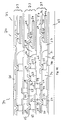
- One such known connection method is shown in Fig. 1 which is described in EP 631 310. It includes a cube of glued chips 1 with connections on one of the sides of the cube which is perpendicular to the layers of chips. The side connection connects through to the output pins 3 of a carrier 2.
- the cube is manufactured in the following way. Integrated circuit chips are formed on the upper surface of a wafer.
- each layer of the stack includes both a chip and also a carrier (semiconductor wafer) for that chip.
- a three-dimensional memory packaging is known from the article by Robert Burns, Warren Chase and Dean Frew, entitled “Utilising three-dimensional memory packaging and silicon on silicon technology for next generation recording devices", ICMCM Proceedings 1992, pages 34 to 40.
- the known device is shown schematically in Fig. 2 and includes a 3D memory 5 connected by solder to the X and Y wiring or “routing", 6, 7 and the ground and source potential, 8, 9 of an MCM substrate 10 which may be built up on a silicon substrate 11.
- the individual layers of the 3D memory 5 are stacked perpendicularly to the substrate 10 so that the complete assembly takes up quite a lot of space in the direction perpendicular to the substrate 10.
- a semiconductor package stack module is known from EP 729 184 in which a large scale integrated circuit (LSI) is mounted via fine bumps on a ceramic carrier substrate or a flexible carrier film on which wiring conductors are formed.
- LSI large scale integrated circuit
- a plurality of such carrier substrates or carrier films are connected to each other by bumps via through holes which are electrically connected to the wiring conductors, thereby completing a three-dimensional stack module.
- This stack takes up quite a lot of room as each layer is relatively thick as it includes both a carrier layer and a chip. Further, the connections are made on one side of the cube resulting in the layers of chips being perpendicular to the substrate.
- ultra-thin substrates in particular semiconductor substrates such as semiconductor grade silicon
- semiconductor substrates such as semiconductor grade silicon
- transfer of more than one layer to form a stack is particularly difficult as the previous transferred layer does not provide a perfectly flat base such that any attempt to transfer the next ultra-thin substrate may result in damage to this layer.
- a removable epoxy is used to attach the glass carrier and this is removed by subjecting the epoxy adhesive to UV or microwave radiation, or chemicals (not specified) to destroy the adhesive properties of the epoxy layer.
- the epoxy layer is then removed by one of the methods described above.
- This known technique makes use of aggressive chemicals and complex procedures which means that the TFT's have to be protected by special layers. This makes the method inconvenient for commercial production. Further, no method is described of how to stack one layer of TFT's on another to form a three-dimensional structure of active devices. In fact, due to the use of aggressive chemicals the procedure is unsuitable for forming three-dimensional active structures.
- the present invention may provide a method of transfer of a first planar substrate with two major surfaces to a second substrate, comprising the steps of: forming the first planar substrate; attaching one of the major surfaces of the first planar substrate to a carrier by means of a release layer; attaching the other major surface of the first substrate to the second substrate with a curable polymer adhesive layer; partly curing the polymer adhesive layer, and disconnecting the release layer from the first substrate to separate the first substrate from the carrier followed by curing the polymer adhesive layer.
- the method may include the step of the curable adhesive being applied to the second substrate before the attaching step.
- the first substrate is preferably an ultra-thin semiconductor substrate formed by thinning a semiconductor substrate which is supported by the carrier and the release layer during the thinning operation.
- the present invention may also provide a multi-layer thin film device comprising: a plurality of layers, each layer including a planar three-dimensional interconnect portion having "X", "Y” and “Z” connection routings and adjacent thereto a planar semiconductor device portion, the semiconductor device portion being connected to the interconnect portion in each layer, the "X" and “Y” routings lying in the plane of the interconnect portion and the "Z” routing being perpendicular thereto, the "Z" routing in each interconnect portion being selectably distributed throughout the interconnect portion.
- the present invention also includes a method of forming a multi-layer thin film device; comprising the steps of
- the present invention may also include a multi-layer thin film device comprising: a plurality of layers forming a stack of layers, each layer including a planar semiconductor device portion on an ultra-thin substrate, the planar semiconductor device portion having a metallisation layer, each layer being adhered to the next layer by a cross-linked polymeric adhesive layer; and a groove within the stack, the metallisation layer of each semicoductor device portion being exposed in said groove.
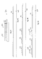
- Figs. 1 and 2 show prior art devices.
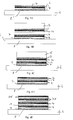
- Figs. 3A to 3G show schematically manufacturing steps for transferring an ultra-thin substrate in accordance with an embodiment of the present invention.
- Figs. 4A to 4E show schematically manufacturing steps to form a multi-layer stack of thin substrates in accordance with another embodiment of the present invention.
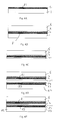
- Figs. 5A to 5F show schematic manufacturing steps for transferring ultrathin substrates in accordance with another embodiment of the present invention.
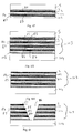
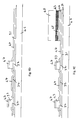
- Figs. 6A to 6I show schematic manufacturing steps for transferring ultrathin substrates in accordance with another embodiment of the present invention.
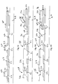
- Figs. 7A to 7I show schematic manufacturing steps for transferring ultrathin substrates in accordance with another embodiment of the present invention.
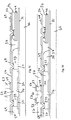
- Fig. 8 is a schematic cross-sectional representation of a multi-layer thin film device in accordance with an embodiment of the present invention.
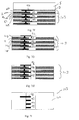
- Figs. 9A to 9K show schematic manufacturing steps for manufacturing the multi-layer thin film device shown in Fig. 8.
- Figs. 10A and B are schematic top- and side views of a multi-layer thin film device as shown in Fig. 8.
- Fig. 3A shows a planar first substrate 1.
- Substrate 1 may be one of a variety of suitable substrates, e.g. single crystal semiconductor silicon, semiconductor amorphous silicon, silicon on glass, silicon on sapphire or quartz.
- Active devices and/or passive devices 2 are formed in or on one major surface of the substrate 1 by conventional means such as, but not limited to, conventional semiconductor processing techniques, for example epitaxy.
- the devices 2 may be any suitable active or passive devices which may include a plurality of active and passive elements, e.g.
- Substrate 1 may be a semiconductor wafer and the active devices 2 may be a plurality of integrated circuits or dies arranged on the wafer 1 in a pattern as is well known to the skilled person and which will be described in more details with reference to the second embodiment.
- Substrate 1 is next attached to a carrier substrate 5 by means of a release layer 3 as shown schematically in Fig. 3B.
- Release layer 3 is preferably a layer which may be removed easily thermally and/or by solvents or by any other technique which provides low chemical, mechanical and thermal stress to the active devices 2.
- a thermal removal technique for release layer 3 should preferably not involve heating the devices 2 above 250°C, more preferably not above 200 °C, and most preferably not above 150°C.
- Release layer 3 may be a photoresist layer having a good thermal stability, e.g. a melting point of 120°C or more and preferably being soluble in a common solvent such as acetone.
- a suitable material for release layer 3 is photoresist A24562, available from Hoechst, Germany.
- the release layer 3 may be applied by spin-coating from a solvent solution. Alternatively, release layer 3 may be made of a wax.
- Carrier 5 may be any suitable substrate, e.g. a further semiconductor substrate such as a single crystal silicon substrate, silicon on sapphire, silicon on glass, an alumina, a glass or a quartz substrate or a metal substrate such as aluminium.
- a further semiconductor substrate such as a single crystal silicon substrate, silicon on sapphire, silicon on glass, an alumina, a glass or a quartz substrate or a metal substrate such as aluminium.
- the other major surface of the substrate 1 is now optionally thinned by conventional grinding and polishing techniques, by reactive ion etching, by chemical-mechanical polishing (CMP) or similar to form an ultra-thin planar substrate 1,2 as shown schematically in Fig. 3C composed of the active devices 2 and what is left of the substrate 1.
- Substrate 1 may also be cleaved from the active devices 2 using any conventional technique, such as the mechanical separation technique using porous silicon as is known from EP 797 258, and substrate 1 may be re-used.
- the ultra-thin substrate 1,2 may have a thickness in the range 5-25 micron, and is mechanically supported and protected by the carrier 5.
- the substrate thinning process may result in a thinned substrate 1,2 which from now on will be called a die 4, glued upside down on a supporting silicon chip carrier 5 using the spin-on release layer 3.
- a die 4 glued upside down on a supporting silicon chip carrier 5 using the spin-on release layer 3.
- the thinning step may be omitted or may be terminated before an ultra-thin die 4 is obtained.
- the die 4 with its devices 2 are attached to a second substrate 6 as shown schematically in Fig. 3E.
- Accurate placement of the die 4 on the second substrate 6 is preferable and may include the steps of:
- the adhesive layer 7 should preferably have a high adhesion strength, in particular sheer strength, low thermal resistance and be a highly uniform layer in order to allow stacking of further substrates on the top thereof.
- a flip-chip aligner/bonder may be used, for example as an FCG machine supplied by Karl Suss, France.
- FCG machine supplied by Karl Suss, France.
- Such a bonder has an alignment accuracy better than +/- 3 ⁇ m.
- the stated machine is precise enough to get an overall accuracy of placement of +/- 10 ⁇ m, taking into account possible movements of the die 4 after placement, e.g. during the removal of the carrier or the curing of the adhesive layer.
- Another advantage of this known machine is the good controllability of the die and second substrate temperature, as well as the applied force during bonding. Furthermore, temperature and force may be varied as a function of time in a rather general fashion.
- an adhesive layer 7 is preferred which is planarisable, is preferably easily applied, e.g. by spin-coating, is preferably resistant to any chemicals or thermal conditions used to remove or weaken the release layer 3, and is preferably insulating and has a high thermal conductivity.
- the adhesive layer 7 is crosslinkable, i.e. curable, and that on-cure shrinkage is not excessive and there is no outgassing of gasses or water vapour or any bubble formation.
- adhesive layer 7 is preferably a polymer adhesive layer.
- a BCB material is preferred. In particular, CycloteneTM grades supplied by Dow of Dow, Midland, USA are preferred.
- BCB may be applied in thin layers by spin-coating with excellent control on uniformity as shown schematically in Fig. 3D and explained below.
- the planarisation achievable with BCB is better than or equal to 80% and is usually better than 85%. If two layers of BCB are applied, planarisation better than 90% can be achieved.
- Second substrate 6 may have an uneven upper surface as shown schematically in Fig. 3D as indicated by the irregularities 8.
- the adhesive layer 7 is preferably sufficiently planarisable to cover such irregularities 8 while providing a flat upper surface.
- One disadvantage of BCB is the poor thermal properties of the polymer. This may be overcome by using a very thin layer and optionally by the use of thermal conductors 8 in the layer 7 of BCB as shown schematically in Figs. 3D and E. These thermal conductors are of such a height that they extend through a substantial portion of the thickness of the BCB layer 7 but not completely so that an insulating layer of BCB is still provided over the conductors 8.
- the purpose of the conductors 8 is to reduce the thermal resistance of the adhesive layer 7, thus improving the thermal properties of the die 4 when it is attached and operating.
- the BCB layer 7 is kept tacky and soft until the die attach process is finalised. Further, it is preferred to remove the carrier 5 and the release layer 3, without damage to the BCB layer 7.
- a suitable procedure to meet these requirements is:
- the above process may be repeated to produce a three dimensional stack 9 of dies 4 as shown schematically in Figs. 4A to E.
- the starting point is the product of Fig. 3F onto which a further thin layer 17 of BCB is spun-coated (Fig. 4A) in order to planarise the surface and to provide an adhesive layer 17 for the next die 14 as shown schematically in Fig. 4B.
- Die 14 is applied to the adhesive layer 17 having been pre-attached to a carrier 15 using a release layer 13 such as soluble photoresist as described above for carrier 5, release layer 3 and die 4 (Fig. 4C).
- the carrier 15 and the photoresist 13 are then removed as described above and the adhesive layer 17 baked to complete cure (Fig. 4D).
- Each individual layer of stack 9 (each made up of a die including active devices and an adhesive layer) may be thin, e.g. less than 300 microns, preferably less than 150 microns and more preferably less than 100 microns thick and typically 25 microns thick resulting in a very compact device in comparison with conventional stacks as well as having excellent thermal properties.
- Thermal bridges 8 may be placed in any of the adhesive layers 7, 17, etc. to improve the thermal characteristics of the stack 9.
- the adhesive polymer layer 7 was applied to the second substrate 6 in step S3 however the present invention also includes applying the adhesive layer 7 (e.g. by spin-coating) to the surface of die 4 which has been exposed by thinning.
- the transfer of the die 4 to the second substrate 6 may then be carried out in accordance with steps S4 to S9 above.
- the application of the adhesive as described for step S3 is preferred as it planarises the surface of substrate 6.
- the planarisation of the thinned surface of the die 4 is normally achieved adequately during the thinning process of substrate 1 and therefore a further planarisation is not necessary. If necessary a polishing step may be applied after thinning substrate 1 in order to improve the planarisation of the surface of the die 4.
- a plurality of devices 22 are formed in a wafer 21 as shown schematically in Fig. 5A.
- Devices 22 may be similar to any of the devices 2 described above with respect to the first embodiment.
- Wafer 21 may be any suitable wafer such as, for example, a single crystal silicon wafer, a silicon on glass or a silicon on sapphire wafer or a quartz wafer.
- the wafer 21 may be diced to produce individual thick dies 24 (Fig. 5B). Each die 24 may be processed as above by attaching a carrier 5 with a release layer 3 and transferred and attached to a second substrate 6 and optionally to form a stack 9 as described above for the first embodiment.
- all the dies 24 may be attached to a carrier 25 using a release layer 23, e.g. photoresist, as shown schematically in Fig. 5C.
- Substrate 21 may then be thinned by any conventional technique (Fig. SE).
- the laminate may then be sawn into die laminates 25, 23, 21 as shown in Fig. 5E.
- Each of these die laminates 25, 23, 21 is then cleaned to remove any debris caused by the sawing operation and attached to a second substrate 26 by the methods described above using a polymer adhesive layer 27 (Fig. 5F) including removal of the carrier 25 and release layer 23.
- the wafer of Fig. 5C may be sawn into die laminates and the substrate 21 of each laminate thinned individually before attachment to a further substrate 26 using an adhesive layer 27 and removal of the carrier 25 and release layer 23 (not shown).
- the starting material is a substrate 1, e.g. a semiconductor substrate, onto which is formed or deposited a layer 2 including active or passive devices (Fig. 6A), e.g. memory cells.
- a metallisation layer may be applied to the surface of the layer 2 of active and/or passive devices and may include one or more bonding pads 81.
- Substrate 1 is attached to a carrier 5 by a release layer, e.g. solvent removable photoresist, as described above (Fig. 6B).
- Substrate 1 is then thinned by conventional techniques, such as chemical or mechanical grinding and/or polishing, to form an ultra-thin substrate 101 which may have a thickness of about 5 to 25 micron (Fig. 6C).
- a second substrate 82 e.g. a semiconductor substrate, is prepared with a layer 83 of active or passive devices (Fig. 6D).
- An optional metallisation layer with one or more bonding pads 85 may also be provided.
- This substrate 82 is attached to the thinned side of substrate 101 using an adhesive layer 84, e.g. a polymer adhesive layer such as BCB (Fig. 6E) which is softened by heating before adhesion.
- Substrate 82 is then thinned to form a second ultra-thin substrate 102 (Fig.
- each device layer in the stack 103 may include one or more bonding pads 81, 85, 86, 87.
- the adhesive layers 84...105 in the stack are now baked at a suitable temperature, e.g. about 120°C, to make them resistant to solvents such as acetone.
- the carrier 5 is then removed from the stack by dissolving away the release layer 3 in a suitable solvent, e.g. acetone (Fig. 6H).
- the stack 103 is then baked to completely cross-link the adhesive layers 84...105.
- the stack 103 may be etched or grooved to form a groove 106 through all the layers of stack 103 (Fig. 6I).
- This groove 106 may allow access to all the metallisation device layers in stack 103, e.g. the bonding pads 81, 85, 86, 87 may be exposed.
- Contact metallisation (not shown) may be applied to the surfaces of the groove 106 to make contacts with the metallisations of the device layers.
- the starting material is a substrate 1 with a layer 2 deposited or formed thereon or therein which may include active or passive devices.
- the layer 2 may also include a metallisation layer including one or more bonding pads 81.
- a trench 91 is then formed, e.g. by etching, ion milling or similar through device layer 2 into substrate 1 (Fig. 7A).
- a layer 107 of insulating material, e.g. a BCB layer is then deposited over the complete surface of the device layer 2 filling the trench 91 (Fig. 7B).
- the insulating layer 107 is then patterned by conventional techniques to form a via hole above the bonding pad 81.
- a metallisation layer is then deposited and patterned to form a metallisation strip 92 (Fig. 7C).
- the strip 92 extends so that it overlaps the trench 91.
- the top surface of insulating layer 107 is then adhered to a carrier 5 by a release layer 3 such as a solvent release layer, e.g. photoresist (Fig. 7D).
- Substrate 1 is then thinned by conventional techniques to form an ultra-thin substrate 101. The thinning should be sufficient to make contact with the bottom of the trench of the insulating layer 107 (Fig. 7E).
- a further substrate is prepared with a device layer 83, an insulating layer 108 and a metallisation strip 92 which is attached to the under side of the substrate 101 by a polymeric adhesive layer, e.g. BCB, 84 (Fig. 7F).
- the substrate is thinned to an ultra-thin substrate 109.
- a stack 103 of device layers 2, 83..., thinned substrates 101, 109... and insulating layers 107, 108... is obtained (Fig. 7F).
- Each layer may have one or more metallisation strips 92-95.
- the trenches of the insulating layers 107, 108 are preferably aligned one above the other.
- the adhesive layers 84.. are partially cross-linked by raising the temperature of the stack 103, e.g. to 120°C. After partial cross-linking the carrier 5 is removed by a solvent such as acetone (Fig. 7G).
- the aligned trenches are then etched or ion milled to expose the metallisation strips 92-95 (Fig. 7H).
- Fig. 7I which is a top view of the device, the metallisation strips 92-95 may be offset from each other, so that each may be accessed separately. A suitable metallisation may then be applied (not shown).
- the above method of attaching ultra-thin dies to a substrate to form a stack may be used to form a multi-layer thin film device 70 including a three-dimensional structure which includes a three-dimensional interconnect 71 for connecting to the semiconductor device portion 72 which may include a stack of semiconductor device layers 73 as shown schematically in Fig. 8.
- the multi-layer thin film device 70 is very compact and has excellent thermal properties.
- the three-dimensional interconnect 71 in accordance with the present invention includes connection paths or wiring layers or connections in all three orthogonal space filling dimensions, i.e. X, Y and Z routing, for interconnecting the semiconductor devices in the device layers 73 among themselves and to external.
- a substrate 46 is first prepared.
- This substrate 46 may be any suitable substrate, in particular, any substrate which may be used for MCM processing such as single crystal silicon, silicon on glass, silicon on sapphire, alumina, aluminium.
- An insulating layer 31 is then optionally deposited (Fig. 9A).
- Layer 31 may be any suitable insulating layer such as, for example, an oxide layer or a spin-coated BCB layer or layers which has (have) a high level of planarisation, e.g. 80% or better, more preferably 85% or better.
- the insulating layer 31 may have a thickness of between 1 and 5.
- a first interconnection metallisation 32 is deposited onto the insulating layer 31 and patterned in accordance with conventional techniques (Fig. 9B).
- the first interconnection metallisation 32 may include a 2 micron Ti/Cu/Ti laminate.
- the first metallisation 32 may be produced by magnetron sputtering of a 30 nm/2 micron/30 nm Ti/Cu/Ti wiring layer with a wiring line thickness of 10 micron and a wiring line spacing of 20 micron.
- the first metallisation may be formed by pattern plating copper wiring lines. First a tin seed layer is sputtered followed by the deposition and patterning of a 15 micron thick resist. The resist is patterned and the copper metal is plated in the resist openings using a jet-plating method.
- the wiring lines may be a small as 10 micron in width and 10 micron in thickness.
- the first interconnection metallisation 32 forms part of the X and Y routing of the interconnect 71 (the dimensions X and Y are orthogonal and lie in the plane of the substrate 46. The Z direction is perpendicular to this plane.).
- the X and Y routing 32 may be applied typically with a pitch of 50 microns or less and the position of the individual metallisation elements may be freely selected.
- Next metal, e.g. copper, studs 33 are plated onto at least a part of the first interconnection metallisation 32 (Fig. 9C).
- the height of the metals studs 33 is preferably chosen to be approximately the same thickness as the thinned die 44 which will be applied in the next steps.
- the studs 33 form part of the Z routing of the interconnect 71 in accordance with the present invention.
- the Z routing in accordance with the present invention may typically have a pitch of 100 micron or less.
- the studs 33 may be produced in a jet-plating cell. Alternatively a conventional parallel plate plating cell may be used. Between the anode of the cell and a substrate 46 an anode shield may be placed. This anode may be a solid plate with holes approximately the size of the substrate to be plated. This is done to obtain a more homogeneous plating.
- the obtained plating results obtained in this bath may be summarised as :
- the plating may be performed using a thick photoresist such as AZ4562.
- This resist is applied as a 15 to 20 ⁇ m thick layer. It has an excellent resolution and a high resistance to plating solutions.
- Studs 33 may be in the range 10 to 80 ⁇ m in diameter with a thickness of between 5 ⁇ m and 12 ⁇ m in height.
- a thin coating of a polymer adhesive layer 47 is now applied to the complete surface of the substrate 46 (Fig. 9D).
- the adhesive layer 47 is preferably a thin polymer layer such as a spin-coated BCB layer.
- the BCB layer 47 preferably has a thickness of 1 to 5 micron.
- CycloteneTM 3202 from Dow is used for the layer 47.
- the BCB layer 47 is now pre-baked for 30 min at 30C.
- a thinned die 44 is now transferred to, aligned with and attached to the BCB layer 47 by any of the techniques for transfer of ultra-thin substrates as described above (Fig. 9E).
- the thinned die 44 is attached onto the soft BCB layer 47 using carrier 45 as a support attached to the die 44 by a release layer 43, e.g. photoresist.
- Die 44 is preferably an integrated circuit having die bond pads 48 for electrical connection thereto.
- the temperature at BCB - die interface is preferably maintained at about 70°C, and the applied pressure to the die 44 is preferably about 80 kPa.
- the BCB layer 47 is now post-baked the for 2 hours at 120C (below the melting temperature of the release layer 43) in a nitrogen atmosphere. After this thermal treatment, the adhesive layer 47 is partly hardened and it is resistant to solvents such as acetone.
- the carrier 45 may be removed by placing the laminate 43, 44, 45, 46, 47 in a solvent such as acetone but the present invention is not limited thereto.
- the carrier 45 may be removed with a vacuum pipette. Any remaining photoresist on the surface of the die 44 may be removed by dipping in an acetone bath at room temperature.
- the BCB layer 47 is completely cured using the BCB curing profile recommended by the supplier of the BCB (Fig. 9F).
- a thick photo-BCB layer 34 is now applied to the complete surface of substrate 46, e.g. by spin-coating.
- Photo-BCB is a photosensitive BCB material available, for instance, from Dow (CycloteneTM 4202 is particularly preferred).
- the photo-BCB layer 34 is patterned and vias 35 opened on studs 33 and a cavity 36 opened on and around the die 44 (Fig. 9G).
- a second thin photo-BCB layer 37 is deposited on the complete surface of the substrate 46 and patterned to open the vias 35 on the studs 33 again and to open vias 38 on the die bond pads 48 (Fig. 9H).
- the upper surface of the substrate 46 is now dry etched to remove any BCB residues in the via holes 35, 38 and to remove any adhesive layer residues on the studs 33. Because of the height of the studs 33, the adhesive layer 47 on top of the studs 33 will be significantly thinner than below the die 44.
- a second metallisation layer 49 is applied which contacts the studs 33 and the die pads 48 (Fig. 9I).
- This metallisation layer may be a Ti/Cu/Ti layer, e.g. 30nm/2 micron/30 nm respectively.
- the second metallisation layer 49 forms part of the X and Y routing of the interconnect 71 in accordance with the present invention.
- the X and Y routing may have a pitch of 50 microns or less.
- Interlayer studs 53 are now plated onto the second metallisation layer 49 to provide a part of the Z routing of the interconnect 71 between the layers 73 of the final device 70. Studs 53 do not have to be aligned with studs 33 and their position may be chosen freely.
- the Z routing may have a pitch of 100 microns or less.
- the upper surface of the substrate 46 is planarised with a spun-coated BCB layer 57 (Fig. 9J) which will also form the planarised base for placing the next die 54
- the sequence of operations described above may now repeated with the next layer of the semiconductor device portion 72 and the interconnect 71 which includes a third metallisation layer 52, a thin polymer adhesive layer (BCB) 67, a thinned die 54 with die pads 59, studs 63, first photo-BCB layer 64, a second photo-BCB layer 65 and a fourth interconnect metallisation 69.
- the thinned die 54 need not be in alignment with the die 44. Instead its position may be freely chosen.
- the studs 63 need not be aligned with the studs 53 or 33, their position may be freely chosen. More layers can be added to form a final three dimensional structure of a multilayer thin film device 70 as shown schematically in Fig. 9K.
- the final layer 75 may be a passivation layer to protect the complete device 70 and to reduce stresses therein.
- Each layer 73 of the device 70 may have a thickness of less than 300 microns, preferably less than 150 microns and most preferably less than 100 microns.
- a multi-layer thin film device 70 according to the fourth embodiment is shown schematically in top view in Fig. 10A and side-view in Fig. 10B.
- the device layers 73 are connected electrically to power and ground lines 112, 113 as well as to X, Y, and Z routings 114, e.g. signal wiring typically in the form of one or more busses. To avoid cross-talk it is preferred if the signal routings 114 are microstrip lines or striplines. Both the upper surface and the lower surface of each device layer 73 may be provided with metallisation layers 111 for connection to the power or ground wires 112, 113 and signal routings 114.
- the above multi-layer thin film device 70 has an interconnect 71 in which the X, Y and Z routing a freely selectable in their position. Further, the semiconductor devices, e.g. the dies 44, 54 of a layer 73 are ultra-thin and may be safely transferred by the transfer method described with reference to the above embodiments. This provides for a very compact design. Further, the compact design provides a multi-thin film device 70 with excellent thermal properties.
- the multi-layer thin film device 70 has been described above with reference to only one die per device layer 73.
- the present invention also includes a plurality of dies in one or more layers of device 70.
- thermal bridges 8 have benn described with reference to the stack and manufacturing method shown in Fig. 4 but the present invention specifically includes using thermal bridges 8 in any of the polymeric adhesive layers in each or any of the embodiments of the present invention.
Abstract
The present invention provides a method of transfer of a first planar substrate with two
major surfaces to a second substrate, comprising the steps of: forming the first planar
substrate, attaching one of the major surfaces of the first planar substrate to a carrier by
means of a release layer; attaching the other major surface of the first substrate to the
second substrate with a curable polymer adhesive layer; partly curing the polymer adhesive
layer, disconnecting the release layer from the first substrate to separate the first substrate
from the carrier, followed by curing the polymer adhesive layer.
The method may be used to form a stack of dies (4, 14...) which are adhered together by
cured polymeric layers (7, 17). Each die (4, 14 ...) may include a device layer and an ultrathin
substrate manufactured and assembled by the method described above.
Description
- The present invention relates to a method of transferring ultra-thin substrates, in particular, semiconductor substrates including active devices as well as a multi-layer thin film device manufacturable using the transfer method.
- In order to try and increase density of packing of integrated circuits and semiconductor chips it is known to form a so called "cube" package consisting of a number of passivated device chips glued together in a stacked configuration. Conventionally these devices are connected via one of the side surfaces of the cube which is perpendicular to the layers of chips. One such known connection method is shown in Fig. 1 which is described in EP 631 310. It includes a cube of glued chips 1 with connections on one of the sides of the cube which is perpendicular to the layers of chips. The side connection connects through to the
output pins 3 of acarrier 2. The cube is manufactured in the following way. Integrated circuit chips are formed on the upper surface of a wafer. Next a polymer adhesive material is applied to the top of the completed chips. The wafer is then diced and the plurality of integrated circuit chips are then stacked, one on top of another, using the adhesive to bond them together. The resulting cube structure is rather bulky as each layer of the stack includes both a chip and also a carrier (semiconductor wafer) for that chip. - A three-dimensional memory packaging is known from the article by Robert Burns, Warren Chase and Dean Frew, entitled "Utilising three-dimensional memory packaging and silicon on silicon technology for next generation recording devices", ICMCM Proceedings 1992,
pages 34 to 40. The known device is shown schematically in Fig. 2 and includes a3D memory 5 connected by solder to the X and Y wiring or "routing", 6, 7 and the ground and source potential, 8, 9 of anMCM substrate 10 which may be built up on a silicon substrate 11. As with the device known from EP-631 310 the individual layers of the3D memory 5 are stacked perpendicularly to thesubstrate 10 so that the complete assembly takes up quite a lot of space in the direction perpendicular to thesubstrate 10. - A semiconductor package stack module is known from EP 729 184 in which a large scale integrated circuit (LSI) is mounted via fine bumps on a ceramic carrier substrate or a flexible carrier film on which wiring conductors are formed. A plurality of such carrier substrates or carrier films are connected to each other by bumps via through holes which are electrically connected to the wiring conductors, thereby completing a three-dimensional stack module. This stack takes up quite a lot of room as each layer is relatively thick as it includes both a carrier layer and a chip. Further, the connections are made on one side of the cube resulting in the layers of chips being perpendicular to the substrate.
- The above devices suffer from the problem that the cube packages are formed from relatively thick layers which not only makes them bulky but also negatively affects their thermal properties.
- The handling of ultra-thin substrates, in particular semiconductor substrates such as semiconductor grade silicon, is difficult as such layers are brittle and are easily damaged. In addition the transfer of more than one layer to form a stack is particularly difficult as the previous transferred layer does not provide a perfectly flat base such that any attempt to transfer the next ultra-thin substrate may result in damage to this layer.
- One method of transferring thin semiconductor substrates including active devices is described in US 5,256,562. The method is not described in detail but it includes formation of thin film transistors on a first substrate. The transistor side of the substrate is then glued to a carrier substrate using an epoxy adhesive. The carrier may be glass. The first substrate would then appear to be removed although this step is not described and the carrier and the TFT's is transferred to a second substrate and adhered thereto with another adhesive (not specified). The glass carrier is then removed using hydrofluoric acid and the epoxy adhesive removed by oxygen plasma, sulphuric acid or boiling trichlorethylene. Alternatively, a removable epoxy is used to attach the glass carrier and this is removed by subjecting the epoxy adhesive to UV or microwave radiation, or chemicals (not specified) to destroy the adhesive properties of the epoxy layer. The epoxy layer is then removed by one of the methods described above. This known technique makes use of aggressive chemicals and complex procedures which means that the TFT's have to be protected by special layers. This makes the method inconvenient for commercial production. Further, no method is described of how to stack one layer of TFT's on another to form a three-dimensional structure of active devices. In fact, due to the use of aggressive chemicals the procedure is unsuitable for forming three-dimensional active structures.
- It is an object of the present invention to provide a method of assembly of integrated circuit chips which allows the production of the stack of such chips with high density.
- It is a further object of the present invention to provide a semiconductor device and a method of making the same which includes a three-dimensional structure of active and passive electronic devices which takes up less room than the known three-dimensional structures.
- It is still a further object of the present invention to provide a method of safe transfer of very thin substrates, especially semiconductor substrates.
- It is yet a further object of the present invention to provide a semiconductor device and a method of making the same having a three-dimensional structure of active and passive electronic devices which has better thermal and/or electrical properties than conventional devices.
- The present invention may provide a method of transfer of a first planar substrate with two major surfaces to a second substrate, comprising the steps of: forming the first planar substrate; attaching one of the major surfaces of the first planar substrate to a carrier by means of a release layer; attaching the other major surface of the first substrate to the second substrate with a curable polymer adhesive layer; partly curing the polymer adhesive layer, and disconnecting the release layer from the first substrate to separate the first substrate from the carrier followed by curing the polymer adhesive layer.
- The method may include the step of the curable adhesive being applied to the second substrate before the attaching step. The first substrate is preferably an ultra-thin semiconductor substrate formed by thinning a semiconductor substrate which is supported by the carrier and the release layer during the thinning operation.
- The present invention may also provide a multi-layer thin film device comprising: a plurality of layers, each layer including a planar three-dimensional interconnect portion having "X", "Y" and "Z" connection routings and adjacent thereto a planar semiconductor device portion, the semiconductor device portion being connected to the interconnect portion in each layer, the "X" and "Y" routings lying in the plane of the interconnect portion and the "Z" routing being perpendicular thereto, the "Z" routing in each interconnect portion being selectably distributed throughout the interconnect portion.
- The present invention also includes a method of forming a multi-layer thin film device; comprising the steps of
- step 1: attaching a semiconductor device to a substrate;
- step 2: providing a planar three-dimensional interconnect portion on the substrate
having "X", "Y" and "Z" connection routings adjacent to the semiconductor device, the
semiconductor device being connected to the interconnect portion, the "X" and "Y"
routings lying in the plane of the interconnect portion and the "Z" routing being
perpendicular thereto, the "Z" routing in each interconnect portion being selectably
distributed throughout the interconnect portion; and repeating
steps 1 and 2 for each layer. -
- The present invention may also include a multi-layer thin film device comprising: a plurality of layers forming a stack of layers, each layer including a planar semiconductor device portion on an ultra-thin substrate, the planar semiconductor device portion having a metallisation layer, each layer being adhered to the next layer by a cross-linked polymeric adhesive layer; and a groove within the stack, the metallisation layer of each semicoductor device portion being exposed in said groove.
- The dependent claims define further individual embodiments of the present invention.
- The present invention its advantages and embodiments will now be described with reference to the following drawings.
- Figs. 1 and 2 show prior art devices.
- Figs. 3A to 3G show schematically manufacturing steps for transferring an ultra-thin substrate in accordance with an embodiment of the present invention.
- Figs. 4A to 4E show schematically manufacturing steps to form a multi-layer stack of thin substrates in accordance with another embodiment of the present invention.
- Figs. 5A to 5F show schematic manufacturing steps for transferring ultrathin substrates in accordance with another embodiment of the present invention.
- Figs. 6A to 6I show schematic manufacturing steps for transferring ultrathin substrates in accordance with another embodiment of the present invention.
- Figs. 7A to 7I show schematic manufacturing steps for transferring ultrathin substrates in accordance with another embodiment of the present invention.
- Fig. 8 is a schematic cross-sectional representation of a multi-layer thin film device in accordance with an embodiment of the present invention.
- Figs. 9A to 9K show schematic manufacturing steps for manufacturing the multi-layer thin film device shown in Fig. 8.
- Figs. 10A and B are schematic top- and side views of a multi-layer thin film device as shown in Fig. 8.
- The present invention will be described with reference to certain embodiments and to certain drawings but the present invention is not limited thereto but only by the claims. The drawings are schematic and non-limiting and certain dimensions have been exaggerated for clarity purposes. In particular, methods of transferring thin substrates will be described with reference to the fabrication of a three-dimensional structure of active devices but the present invention is not limited thereto but only by the attached claims.
- A method of forming and transferring an ultra-thin substrate in accordance with a first embodiment of the present invention will be described with reference to Figs. 3A to 3F which show cross-sectional representations of the manufacturing steps required. Fig. 3A shows a planar first substrate 1. Substrate 1 may be one of a variety of suitable substrates, e.g. single crystal semiconductor silicon, semiconductor amorphous silicon, silicon on glass, silicon on sapphire or quartz. Active devices and/or
passive devices 2 are formed in or on one major surface of the substrate 1 by conventional means such as, but not limited to, conventional semiconductor processing techniques, for example epitaxy. Thedevices 2 may be any suitable active or passive devices which may include a plurality of active and passive elements, e.g. an integrated circuit, CMOS transistors, thin film transistors, capacitors, resistors, memory arrays, micro- or nano-engineered devices such as UV or IR sensors, accelerometers, chemical or gas sensors, opto-electronic switches and circuits or similar. Substrate 1 may be a semiconductor wafer and theactive devices 2 may be a plurality of integrated circuits or dies arranged on the wafer 1 in a pattern as is well known to the skilled person and which will be described in more details with reference to the second embodiment. - Substrate 1 is next attached to a
carrier substrate 5 by means of arelease layer 3 as shown schematically in Fig. 3B.Release layer 3 is preferably a layer which may be removed easily thermally and/or by solvents or by any other technique which provides low chemical, mechanical and thermal stress to theactive devices 2. A thermal removal technique forrelease layer 3 should preferably not involve heating thedevices 2 above 250°C, more preferably not above 200 °C, and most preferably not above 150°C. Release layer 3 may be a photoresist layer having a good thermal stability, e.g. a melting point of 120°C or more and preferably being soluble in a common solvent such as acetone. A suitable material forrelease layer 3 is photoresist A24562, available from Hoechst, Germany. Therelease layer 3 may be applied by spin-coating from a solvent solution. Alternatively,release layer 3 may be made of a wax. -
Carrier 5 may be any suitable substrate, e.g. a further semiconductor substrate such as a single crystal silicon substrate, silicon on sapphire, silicon on glass, an alumina, a glass or a quartz substrate or a metal substrate such as aluminium. - The other major surface of the substrate 1 is now optionally thinned by conventional grinding and polishing techniques, by reactive ion etching, by chemical-mechanical polishing (CMP) or similar to form an ultra-thin
planar substrate 1,2 as shown schematically in Fig. 3C composed of theactive devices 2 and what is left of the substrate 1. Substrate 1 may also be cleaved from theactive devices 2 using any conventional technique, such as the mechanical separation technique using porous silicon as is known from EP 797 258, and substrate 1 may be re-used. Theultra-thin substrate 1,2 may have a thickness in the range 5-25 micron, and is mechanically supported and protected by thecarrier 5. For example, the substrate thinning process may result in a thinnedsubstrate 1,2 which from now on will be called adie 4, glued upside down on a supportingsilicon chip carrier 5 using the spin-onrelease layer 3. When anultra-thin die 4 is not required the thinning step may be omitted or may be terminated before anultra-thin die 4 is obtained. - In the next step the
die 4 with itsdevices 2 are attached to asecond substrate 6 as shown schematically in Fig. 3E. Accurate placement of thedie 4 on thesecond substrate 6 is preferable and may include the steps of: - S1. Accurate alignment of the
die 4 to the second substrate 6 (e.g. preferably < +/-10 µm). - S2. Application of a thin
adhesive layer 7 betweendie 4 and the second substrate 6 (e.g. preferably < 5 µm). Theadhesive layer 7 should preferably have a high adhesion strength, in particular sheer strength, low thermal resistance and be a highly uniform layer in order to allow stacking of further substrates on the top thereof. - In order to realise the first requirement, a flip-chip aligner/bonder may be used, for example as an FCG machine supplied by Karl Suss, France. Such a bonder has an alignment accuracy better than +/- 3 µm. The stated machine is precise enough to get an overall accuracy of placement of +/- 10 µm, taking into account possible movements of the
die 4 after placement, e.g. during the removal of the carrier or the curing of the adhesive layer. Another advantage of this known machine is the good controllability of the die and second substrate temperature, as well as the applied force during bonding. Furthermore, temperature and force may be varied as a function of time in a rather general fashion. - For the second requirement, an
adhesive layer 7 is preferred which is planarisable, is preferably easily applied, e.g. by spin-coating, is preferably resistant to any chemicals or thermal conditions used to remove or weaken therelease layer 3, and is preferably insulating and has a high thermal conductivity. Preferably, theadhesive layer 7 is crosslinkable, i.e. curable, and that on-cure shrinkage is not excessive and there is no outgassing of gasses or water vapour or any bubble formation. Further,adhesive layer 7 is preferably a polymer adhesive layer. For theadhesive layer 7, a BCB material is preferred. In particular, Cyclotene™ grades supplied by Dow of Dow, Midland, USA are preferred. One potential advantage of using BCB material is the reduction of the number of materials in the final structure, avoiding any non-compatibility problems as BCB may find use as a general insulating material in other parts of the final device. BCB may be applied in thin layers by spin-coating with excellent control on uniformity as shown schematically in Fig. 3D and explained below. The planarisation achievable with BCB is better than or equal to 80% and is usually better than 85%. If two layers of BCB are applied, planarisation better than 90% can be achieved. -
Second substrate 6 may have an uneven upper surface as shown schematically in Fig. 3D as indicated by theirregularities 8. Theadhesive layer 7 is preferably sufficiently planarisable to coversuch irregularities 8 while providing a flat upper surface. One disadvantage of BCB is the poor thermal properties of the polymer. This may be overcome by using a very thin layer and optionally by the use ofthermal conductors 8 in thelayer 7 of BCB as shown schematically in Figs. 3D and E. These thermal conductors are of such a height that they extend through a substantial portion of the thickness of theBCB layer 7 but not completely so that an insulating layer of BCB is still provided over theconductors 8. The purpose of theconductors 8 is to reduce the thermal resistance of theadhesive layer 7, thus improving the thermal properties of thedie 4 when it is attached and operating. In accordance with the present invention, theBCB layer 7 is kept tacky and soft until the die attach process is finalised. Further, it is preferred to remove thecarrier 5 and therelease layer 3, without damage to theBCB layer 7. A suitable procedure to meet these requirements is: - S3. Spin coat a thin (3 µm)
BCB layer 7 on the surface of thesecond substrate 6 covering anyirregularities 8 and planarising the surface (Fig. 3D). - S4. Pre-bake the
BCB layer 7 for 30 min at 30C to soften the BCB. - S5. "Flip-chip" attach the thinned die 4 (using
carrier 5 as a support) on the soft BCB layer 7 (Fig. 3E). The temperature at BCB - die interface is preferably maintained at about 70°C, and the applied pressure to thedie 4 is preferably about 80 kPa. - S6. Post-bake the
BCB layer 7 for 2 hours at 120C (below the melting temperature of the release layer 3) in a nitrogen atmosphere. After this thermal treatment theadhesive layer 7 is partly hardened and it is resistant to solvents such as acetone. - S7. Remove the
carrier 5 by placing thelaminate release layer 3. Thecarrier 5 may be removed with a vacuum pipette. - S8. Remove any remaining photoresist on the surface of the
die 4 by dipping in an acetone bath at room temperature. - S9. Finally, completely curing the
BCB layer 7 using the BCB curing profile recommended by the supplier of the BCB (Fig. 3F). - In order to test the adhesion strength of this method, some dummy 5x5 mm dies 4 were attached to a
thin BCB layer 7, following the procedure described above. Then, a standard die-shear test was performed. An adhesion force in excess of 100 N was measured for the 5x5 mm device (>4 MPa). Sometimes after removing thecarrier 5 from the thinneddie 4, cracks may appear in thethin BCB layer 7. These disappear, however, after curing of theBCB layer 7 in step S9. This may be explained by the occurrence of some flow of the BCB during the temperature ramp-up of the curing process. - The above process may be repeated to produce a three
dimensional stack 9 of dies 4 as shown schematically in Figs. 4A to E. The starting point is the product of Fig. 3F onto which a furtherthin layer 17 of BCB is spun-coated (Fig. 4A) in order to planarise the surface and to provide anadhesive layer 17 for thenext die 14 as shown schematically in Fig. 4B.Die 14 is applied to theadhesive layer 17 having been pre-attached to acarrier 15 using arelease layer 13 such as soluble photoresist as described above forcarrier 5,release layer 3 and die 4 (Fig. 4C). Thecarrier 15 and thephotoresist 13 are then removed as described above and theadhesive layer 17 baked to complete cure (Fig. 4D). This process may be repeated many times to produce astack 9 of dies 4 as shown in schematically in Fig. 4E. Each individual layer of stack 9 (each made up of a die including active devices and an adhesive layer) may be thin, e.g. less than 300 microns, preferably less than 150 microns and more preferably less than 100 microns thick and typically 25 microns thick resulting in a very compact device in comparison with conventional stacks as well as having excellent thermal properties.Thermal bridges 8 may be placed in any of theadhesive layers stack 9. - In the above description of the first embodiment the
adhesive polymer layer 7 was applied to thesecond substrate 6 in step S3 however the present invention also includes applying the adhesive layer 7 (e.g. by spin-coating) to the surface ofdie 4 which has been exposed by thinning. The transfer of thedie 4 to thesecond substrate 6 may then be carried out in accordance with steps S4 to S9 above. Note, however, that the application of the adhesive as described for step S3 is preferred as it planarises the surface ofsubstrate 6. The planarisation of the thinned surface of thedie 4 is normally achieved adequately during the thinning process of substrate 1 and therefore a further planarisation is not necessary. If necessary a polishing step may be applied after thinning substrate 1 in order to improve the planarisation of the surface of thedie 4. - In accordance with a second embodiment a plurality of
devices 22 are formed in awafer 21 as shown schematically in Fig. 5A.Devices 22 may be similar to any of thedevices 2 described above with respect to the first embodiment.Wafer 21 may be any suitable wafer such as, for example, a single crystal silicon wafer, a silicon on glass or a silicon on sapphire wafer or a quartz wafer. Thewafer 21 may be diced to produce individual thick dies 24 (Fig. 5B). Each die 24 may be processed as above by attaching acarrier 5 with arelease layer 3 and transferred and attached to asecond substrate 6 and optionally to form astack 9 as described above for the first embodiment. Alternatively, all the dies 24 may be attached to acarrier 25 using arelease layer 23, e.g. photoresist, as shown schematically in Fig. 5C.Substrate 21 may then be thinned by any conventional technique (Fig. SE). The laminate may then be sawn intodie laminates laminates second substrate 26 by the methods described above using a polymer adhesive layer 27 (Fig. 5F) including removal of thecarrier 25 andrelease layer 23. Alternatively, the wafer of Fig. 5C may be sawn into die laminates and thesubstrate 21 of each laminate thinned individually before attachment to afurther substrate 26 using anadhesive layer 27 and removal of thecarrier 25 and release layer 23 (not shown). - A third embodiment of the present invention will be described with reference to Figs. 6A to I which is particularly useful for the production of three dimensional memory units. The starting material is a substrate 1, e.g. a semiconductor substrate, onto which is formed or deposited a
layer 2 including active or passive devices (Fig. 6A), e.g. memory cells. A metallisation layer may be applied to the surface of thelayer 2 of active and/or passive devices and may include one ormore bonding pads 81. Substrate 1 is attached to acarrier 5 by a release layer, e.g. solvent removable photoresist, as described above (Fig. 6B). Substrate 1 is then thinned by conventional techniques, such as chemical or mechanical grinding and/or polishing, to form anultra-thin substrate 101 which may have a thickness of about 5 to 25 micron (Fig. 6C). Asecond substrate 82, e.g. a semiconductor substrate, is prepared with alayer 83 of active or passive devices (Fig. 6D). An optional metallisation layer with one ormore bonding pads 85 may also be provided. Thissubstrate 82 is attached to the thinned side ofsubstrate 101 using anadhesive layer 84, e.g. a polymer adhesive layer such as BCB (Fig. 6E) which is softened by heating before adhesion.Substrate 82 is then thinned to form a second ultra-thin substrate 102 (Fig. 6F), e.g. 5 to 25 micron thickness. The above processes are repeated to form astack 103 of device layers attached to asubstrate 104 by anadhesive layer 105 and attached to thecarrier 5 via a release layer 3 (Fig. 6G). Each device layer in thestack 103 may include one ormore bonding pads carrier 5 is then removed from the stack by dissolving away therelease layer 3 in a suitable solvent, e.g. acetone (Fig. 6H). Thestack 103 is then baked to completely cross-link theadhesive layers 84...105. Finally, thestack 103 may be etched or grooved to form agroove 106 through all the layers of stack 103 (Fig. 6I). Thisgroove 106 may allow access to all the metallisation device layers instack 103, e.g. thebonding pads groove 106 to make contacts with the metallisations of the device layers. - A fourth embodiment of the present invention will be described with reference to Figs. 7A to I. The starting material is a substrate 1 with a
layer 2 deposited or formed thereon or therein which may include active or passive devices. Thelayer 2 may also include a metallisation layer including one ormore bonding pads 81. Atrench 91 is then formed, e.g. by etching, ion milling or similar throughdevice layer 2 into substrate 1 (Fig. 7A). Alayer 107 of insulating material, e.g. a BCB layer is then deposited over the complete surface of thedevice layer 2 filling the trench 91 (Fig. 7B). The insulatinglayer 107 is then patterned by conventional techniques to form a via hole above thebonding pad 81. A metallisation layer is then deposited and patterned to form a metallisation strip 92 (Fig. 7C). Thestrip 92 extends so that it overlaps the trench 91.The top surface of insulatinglayer 107 is then adhered to acarrier 5 by arelease layer 3 such as a solvent release layer, e.g. photoresist (Fig. 7D). Substrate 1 is then thinned by conventional techniques to form anultra-thin substrate 101. The thinning should be sufficient to make contact with the bottom of the trench of the insulating layer 107 (Fig. 7E). A further substrate is prepared with adevice layer 83, an insulatinglayer 108 and ametallisation strip 92 which is attached to the under side of thesubstrate 101 by a polymeric adhesive layer, e.g. BCB, 84 (Fig. 7F). The substrate is thinned to anultra-thin substrate 109. - The above process is repeated and continued until a
stack 103 ofdevice layers substrates layers layers stack 103, e.g. to 120°C. After partial cross-linking thecarrier 5 is removed by a solvent such as acetone (Fig. 7G). - The aligned trenches are then etched or ion milled to expose the metallisation strips 92-95 (Fig. 7H). As shown in Fig. 7I which is a top view of the device, the metallisation strips 92-95 may be offset from each other, so that each may be accessed separately. A suitable metallisation may then be applied (not shown).
- In accordance with a fifth embodiment of the present invention the above method of attaching ultra-thin dies to a substrate to form a stack may be used to form a multi-layer
thin film device 70 including a three-dimensional structure which includes a three-dimensional interconnect 71 for connecting to thesemiconductor device portion 72 which may include a stack of semiconductor device layers 73 as shown schematically in Fig. 8. The multi-layerthin film device 70 is very compact and has excellent thermal properties. The three-dimensional interconnect 71 in accordance with the present invention includes connection paths or wiring layers or connections in all three orthogonal space filling dimensions, i.e. X, Y and Z routing, for interconnecting the semiconductor devices in the device layers 73 among themselves and to external. - A preferred method and multi-layer
thin film device 70 in accordance with the fifth embodiment will be described with reference to Figs. 9A toK. A substrate 46 is first prepared. Thissubstrate 46 may be any suitable substrate, in particular, any substrate which may be used for MCM processing such as single crystal silicon, silicon on glass, silicon on sapphire, alumina, aluminium. An insulatinglayer 31 is then optionally deposited (Fig. 9A).Layer 31 may be any suitable insulating layer such as, for example, an oxide layer or a spin-coated BCB layer or layers which has (have) a high level of planarisation, e.g. 80% or better, more preferably 85% or better. The insulatinglayer 31 may have a thickness of between 1 and 5. Afirst interconnection metallisation 32 is deposited onto the insulatinglayer 31 and patterned in accordance with conventional techniques (Fig. 9B). For instance, thefirst interconnection metallisation 32 may include a 2 micron Ti/Cu/Ti laminate. Thefirst metallisation 32 may be produced by magnetron sputtering of a 30 nm/2 micron/30 nm Ti/Cu/Ti wiring layer with a wiring line thickness of 10 micron and a wiring line spacing of 20 micron. Alternatively, the first metallisation may be formed by pattern plating copper wiring lines. First a tin seed layer is sputtered followed by the deposition and patterning of a 15 micron thick resist. The resist is patterned and the copper metal is plated in the resist openings using a jet-plating method. The wiring lines may be a small as 10 micron in width and 10 micron in thickness. - The
first interconnection metallisation 32 forms part of the X and Y routing of the interconnect 71 (the dimensions X and Y are orthogonal and lie in the plane of thesubstrate 46. The Z direction is perpendicular to this plane.). The X and Y routing 32 may be applied typically with a pitch of 50 microns or less and the position of the individual metallisation elements may be freely selected. Next metal, e.g. copper,studs 33 are plated onto at least a part of the first interconnection metallisation 32 (Fig. 9C). The height of themetals studs 33 is preferably chosen to be approximately the same thickness as the thinned die 44 which will be applied in the next steps. Thestuds 33 form part of the Z routing of theinterconnect 71 in accordance with the present invention. The Z routing in accordance with the present invention may typically have a pitch of 100 micron or less. - The
studs 33 may be produced in a jet-plating cell. Alternatively a conventional parallel plate plating cell may be used. Between the anode of the cell and asubstrate 46 an anode shield may be placed. This anode may be a solid plate with holes approximately the size of the substrate to be plated. This is done to obtain a more homogeneous plating. The obtained plating results obtained in this bath may be summarised as : - Plating current 1 A/dm2 : +/- 0.16 µm/min : uniformity over wafer = +/- 6 %
- Plating current 3 A/dm2 : +/- 0.50 µm/min : uniformity over wafer = +/- 15% The plating uniformity between neighbouring features of different size is typically better than 3%. A plating non-uniformity up to 10 % is acceptable for the
-
- In order to realise the
small studs 33, the plating may be performed using a thick photoresist such as AZ4562. This resist is applied as a 15 to 20 µm thick layer. It has an excellent resolution and a high resistance to plating solutions.Studs 33 may be in therange 10 to 80 µm in diameter with a thickness of between 5 µm and 12 µm in height. - A thin coating of a
polymer adhesive layer 47 is now applied to the complete surface of the substrate 46 (Fig. 9D). For instance, theadhesive layer 47 is preferably a thin polymer layer such as a spin-coated BCB layer. TheBCB layer 47 preferably has a thickness of 1 to 5 micron. Preferably, Cyclotene™ 3202 from Dow is used for thelayer 47. TheBCB layer 47 is now pre-baked for 30 min at 30C. A thinneddie 44 is now transferred to, aligned with and attached to theBCB layer 47 by any of the techniques for transfer of ultra-thin substrates as described above (Fig. 9E). For example the thinneddie 44 is attached onto thesoft BCB layer 47 usingcarrier 45 as a support attached to the die 44 by arelease layer 43, e.g. photoresist.Die 44 is preferably an integrated circuit havingdie bond pads 48 for electrical connection thereto. The temperature at BCB - die interface is preferably maintained at about 70°C, and the applied pressure to thedie 44 is preferably about 80 kPa. TheBCB layer 47 is now post-baked the for 2 hours at 120C (below the melting temperature of the release layer 43) in a nitrogen atmosphere. After this thermal treatment, theadhesive layer 47 is partly hardened and it is resistant to solvents such as acetone. Thecarrier 45 may be removed by placing the laminate 43, 44, 45, 46, 47 in a solvent such as acetone but the present invention is not limited thereto. Thecarrier 45 may be removed with a vacuum pipette. Any remaining photoresist on the surface of the die 44 may be removed by dipping in an acetone bath at room temperature. Finally, theBCB layer 47 is completely cured using the BCB curing profile recommended by the supplier of the BCB (Fig. 9F). - A thick photo-
BCB layer 34 is now applied to the complete surface ofsubstrate 46, e.g. by spin-coating. Photo-BCB is a photosensitive BCB material available, for instance, from Dow (Cyclotene™ 4202 is particularly preferred). The photo-BCB layer 34 is patterned andvias 35 opened onstuds 33 and a cavity 36 opened on and around the die 44 (Fig. 9G). A second thin photo-BCB layer 37 is deposited on the complete surface of thesubstrate 46 and patterned to open the vias 35 on thestuds 33 again and to openvias 38 on the die bond pads 48 (Fig. 9H). The upper surface of thesubstrate 46 is now dry etched to remove any BCB residues in the via holes 35, 38 and to remove any adhesive layer residues on thestuds 33. Because of the height of thestuds 33, theadhesive layer 47 on top of thestuds 33 will be significantly thinner than below thedie 44. - Next a
second metallisation layer 49 is applied which contacts thestuds 33 and the die pads 48 (Fig. 9I). This metallisation layer may be a Ti/Cu/Ti layer, e.g. 30nm/2 micron/30 nm respectively. Thesecond metallisation layer 49 forms part of the X and Y routing of theinterconnect 71 in accordance with the present invention. The X and Y routing may have a pitch of 50 microns or less.Interlayer studs 53 are now plated onto thesecond metallisation layer 49 to provide a part of the Z routing of theinterconnect 71 between thelayers 73 of thefinal device 70.Studs 53 do not have to be aligned withstuds 33 and their position may be chosen freely. The Z routing may have a pitch of 100 microns or less. Finally, the upper surface of thesubstrate 46 is planarised with a spun-coated BCB layer 57 (Fig. 9J) which will also form the planarised base for placing the next die 54. - The sequence of operations described above may now repeated with the next layer of the
semiconductor device portion 72 and theinterconnect 71 which includes athird metallisation layer 52, a thin polymer adhesive layer (BCB) 67, a thinned die 54 withdie pads 59,studs 63, first photo-BCB layer 64, a second photo-BCB layer 65 and afourth interconnect metallisation 69. The thinned die 54 need not be in alignment with thedie 44. Instead its position may be freely chosen. Thestuds 63 need not be aligned with thestuds thin film device 70 as shown schematically in Fig. 9K. Thefinal layer 75 may be a passivation layer to protect thecomplete device 70 and to reduce stresses therein. Eachlayer 73 of thedevice 70 may have a thickness of less than 300 microns, preferably less than 150 microns and most preferably less than 100 microns. - A multi-layer
thin film device 70 according to the fourth embodiment is shown schematically in top view in Fig. 10A and side-view in Fig. 10B. The device layers 73 are connected electrically to power andground lines signal routings 114 are microstrip lines or striplines. Both the upper surface and the lower surface of eachdevice layer 73 may be provided with metallisation layers 111 for connection to the power orground wires signal routings 114. The above multi-layerthin film device 70 has aninterconnect 71 in which the X, Y and Z routing a freely selectable in their position. Further, the semiconductor devices, e.g. the dies 44, 54 of alayer 73 are ultra-thin and may be safely transferred by the transfer method described with reference to the above embodiments. This provides for a very compact design. Further, the compact design provides amulti-thin film device 70 with excellent thermal properties. - While the invention has been shown and described with reference to preferred embodiments, it will be understood by those skilled in the art that various changes or modifications in form and detail may be made without departing from the scope and spirit of this invention as defined in the attached claims. For instance, the multi-layer
thin film device 70 has been described above with reference to only one die perdevice layer 73. The present invention also includes a plurality of dies in one or more layers ofdevice 70. - Further, the
thermal bridges 8 have benn described with reference to the stack and manufacturing method shown in Fig. 4 but the present invention specifically includes usingthermal bridges 8 in any of the polymeric adhesive layers in each or any of the embodiments of the present invention.
Claims (15)
- A method of transfer of a first planar substrate with two major surfaces to a second substrate, comprising the steps of:forming the first planar substrate,attaching one of the major surfaces of the first planar substrate to a carrier by means of a release layer;attaching the other major surface of the first substrate to the second substrate with a curable polymer adhesive layer;partly curing the polymer adhesive layer,disconnecting the release layer from the first substrate to separate the first substrate from the carrier, followed bycuring the polymer adhesive layer.
- The method according to claim 1, wherein the curable adhesive is applied to the second substrate before the attaching step.
- The method according to claim 1 or 2, further comprising the step of thinning the first substrate after the attaching step and before the disconnecting step.
- The method according to claim 3, wherein the thinned first substrate has a thickness of 5 to 25 micron.
- The method according to claim 3 or 4, further comprising the step of attaching a second substrate to the thinned exposed surface of the first substrate before the disconnecting step.
- The method according to any previous claim, further comprising the step of attaching a third substrate to the exposed surface of the first substrate after the disconnecting step.
- The method according to any previous claim wherein the first substrate includes active and/or passive electronic devices.
- The method according to any previous claim, wherein the release layer includes a solvent removable layer.
- The method according to any of the previous claims, wherein the first substrate includes a semiconductor substrate.
- The method according to any previous claim, wherein the polymer release layer is BCB.
- A multi-layer thin film device comprising: a plurality of layers, each layer including a planar three-dimensional interconnect portion having "X", "Y" and "Z" connection routings and adjacent thereto a planar semiconductor device portion, the semiconductor device portion being connected to the interconnect portion in each layer, the "X" and "Y" routings lying in the plane of the interconnect portion and the "Z" routing being perpendicular thereto, the "Z" routing in each interconnect portion being selectably distributed throughout the interconnect portion.
- The multi-layer thin film device according to claim 11, wherein the thickness of each layer is 300 microns or less, preferably 150 microns or less, more preferably 100 microns or less and most preferably 50 microns or less.
- A method of forming a multi-layer thin film device; comprising the steps ofstep 1: attaching a semiconductor device to a substrate;step 2: providing a planar three-dimensional interconnect portion on the substrate having "X", "Y" and "Z" connection routings adjacent to the semiconductor device, the semiconductor device being connected to the interconnect portion, the "X" and "Y" routings lying in the plane of the interconnect portion and the "Z" routing being perpendicular thereto, the "Z" routing in each interconnect portion being selectably distributed throughout the interconnect portion; andrepeating steps 1 and 2 for each layer.
- A multi-layer thin film device comprising:a plurality of layers forming a stack of layers, each layer including a planar semiconductor device portion on an ultra-thin substrate, the planar semiconductor device portion having a metallisation layer, each layer of the stack being adhered to the next layer by a cross-linked polymeric adhesive layer; anda groove within the stack, the metallisation layer of each semiconductor device portion being exposed in said groove.
- The multi-layer thin film device according to claim 14 which is a memory.
Priority Applications (5)
| Application Number | Priority Date | Filing Date | Title |
|---|---|---|---|
| EP99201061A EP1041624A1 (en) | 1999-04-02 | 1999-04-02 | Method of transferring ultra-thin substrates and application of the method to the manufacture of a multilayer thin film device |
| EP00201186A EP1041620A3 (en) | 1999-04-02 | 2000-03-31 | Method of transferring ultrathin substrates and application of the method to the manufacture of a multi-layer thin film device |
| JP2000098051A JP4906994B2 (en) | 1999-04-02 | 2000-03-31 | Method for transferring ultrathin substrate and method for manufacturing multilayer thin film device using the method |
| US09/541,995 US6506664B1 (en) | 1999-04-02 | 2000-04-03 | Method of transferring ultra-thin substrates and application of the method to the manufacture of a multi-layer thin film device |
| US10/207,624 US6730997B2 (en) | 1999-04-02 | 2002-07-25 | Method of transferring ultra-thin substrates and application of the method to the manufacture of a multi-layered thin film device |
Applications Claiming Priority (1)
| Application Number | Priority Date | Filing Date | Title |
|---|---|---|---|
| EP99201061A EP1041624A1 (en) | 1999-04-02 | 1999-04-02 | Method of transferring ultra-thin substrates and application of the method to the manufacture of a multilayer thin film device |
Publications (1)
| Publication Number | Publication Date |
|---|---|
| EP1041624A1 true EP1041624A1 (en) | 2000-10-04 |
Family
ID=8240064
Family Applications (1)
| Application Number | Title | Priority Date | Filing Date |
|---|---|---|---|
| EP99201061A Withdrawn EP1041624A1 (en) | 1999-04-02 | 1999-04-02 | Method of transferring ultra-thin substrates and application of the method to the manufacture of a multilayer thin film device |
Country Status (3)
| Country | Link |
|---|---|
| US (2) | US6506664B1 (en) |
| EP (1) | EP1041624A1 (en) |
| JP (1) | JP4906994B2 (en) |
Cited By (40)
| Publication number | Priority date | Publication date | Assignee | Title |
|---|---|---|---|---|
| WO2001056079A2 (en) * | 2000-01-28 | 2001-08-02 | Interuniversitair Micro-Elektronica Centrum | A method for transferring and stacking of semiconductor devices |
| EP1267390A2 (en) * | 2001-06-15 | 2002-12-18 | Philips Corporate Intellectual Property GmbH | Method of transferring a substantially disk-shaped workpiece and apparatus for carrying out such a transfer |
| WO2003036712A1 (en) * | 2001-10-19 | 2003-05-01 | Applied Materials, Inc. | Method and apparatus for dicing a semiconductor wafer |
| FR2837620A1 (en) * | 2002-03-25 | 2003-09-26 | Commissariat Energie Atomique | Transfer of elements from one substrate to another substrate using a carrying substrate with an adhesive layer that can then be degraded to release the element after the transfer is completed |
| WO2004003991A2 (en) * | 2002-06-26 | 2004-01-08 | Infineon Technologies Ag | Electronic component with a housing packaging |
| US6737297B2 (en) | 2000-09-26 | 2004-05-18 | International Business Machines Corporation | Process for making fine pitch connections between devices and structure made by the process |
| WO2004061953A2 (en) * | 2002-12-31 | 2004-07-22 | Massachusetts Institute Of Technology | Method of forming a multi-layer semiconductor structure incorporating a processing handle member |
| US7064055B2 (en) | 2002-12-31 | 2006-06-20 | Massachusetts Institute Of Technology | Method of forming a multi-layer semiconductor structure having a seamless bonding interface |
| US7169248B1 (en) * | 2005-07-19 | 2007-01-30 | Micron Technology, Inc. | Methods for releasably attaching support members to microfeature workpieces and microfeature assemblies formed using such methods |
| FR2895562A1 (en) * | 2005-12-27 | 2007-06-29 | Commissariat Energie Atomique | Method for relaxation of forced thin layer constraint, comprises supplying an intermediate support having relaxing polymer layer, principal face and contact face, and setting in adherent contact of the contact face of the thin layer |
| WO2008045422A2 (en) * | 2006-10-10 | 2008-04-17 | Tessera, Inc. | Edge connect wafer level stacking |
| WO2009017758A2 (en) * | 2007-07-27 | 2009-02-05 | Tessera, Inc. | Reconstituted wafer stack packaging with after-applied pad extensions |
| WO2009020572A2 (en) * | 2007-08-03 | 2009-02-12 | Tessera Technologies Hungary Kft. | Stack packages using reconstituted wafers |
| US7749349B2 (en) | 2006-03-14 | 2010-07-06 | Micron Technology, Inc. | Methods and systems for releasably attaching support members to microfeature workpieces |
| US7759166B2 (en) | 2006-10-17 | 2010-07-20 | Tessera, Inc. | Microelectronic packages fabricated at the wafer level and methods therefor |
| WO2010116662A1 (en) * | 2009-04-06 | 2010-10-14 | Canon Kabushiki Kaisha | Semiconductor device and method for manufacturing semiconductor device |
| US7901989B2 (en) | 2006-10-10 | 2011-03-08 | Tessera, Inc. | Reconstituted wafer level stacking |
| US7952195B2 (en) | 2006-12-28 | 2011-05-31 | Tessera, Inc. | Stacked packages with bridging traces |
| EP2339614A1 (en) * | 2009-12-22 | 2011-06-29 | Imec | Method for stacking semiconductor chips |
| US8043895B2 (en) | 2007-08-09 | 2011-10-25 | Tessera, Inc. | Method of fabricating stacked assembly including plurality of stacked microelectronic elements |
| US8431435B2 (en) | 2006-10-10 | 2013-04-30 | Tessera, Inc. | Edge connect wafer level stacking |
| EP1432032A3 (en) * | 2002-12-19 | 2013-05-22 | Semiconductor Energy Laboratory Co., Ltd. | Semiconductor chip stack and method for manufacturing the same |
| US8466542B2 (en) | 2009-03-13 | 2013-06-18 | Tessera, Inc. | Stacked microelectronic assemblies having vias extending through bond pads |
| US8629543B2 (en) | 2007-06-11 | 2014-01-14 | Invensas Corporation | Electrically interconnected stacked die assemblies |
| US8680662B2 (en) | 2008-06-16 | 2014-03-25 | Tessera, Inc. | Wafer level edge stacking |
| US8680687B2 (en) | 2009-06-26 | 2014-03-25 | Invensas Corporation | Electrical interconnect for die stacked in zig-zag configuration |
| US8704379B2 (en) | 2007-09-10 | 2014-04-22 | Invensas Corporation | Semiconductor die mount by conformal die coating |
| US8729690B2 (en) | 2004-04-13 | 2014-05-20 | Invensas Corporation | Assembly having stacked die mounted on substrate |
| US8884403B2 (en) | 2008-06-19 | 2014-11-11 | Iinvensas Corporation | Semiconductor die array structure |
| US8912661B2 (en) | 2009-11-04 | 2014-12-16 | Invensas Corporation | Stacked die assembly having reduced stress electrical interconnects |
| US9147583B2 (en) | 2009-10-27 | 2015-09-29 | Invensas Corporation | Selective die electrical insulation by additive process |
| US9153517B2 (en) | 2008-05-20 | 2015-10-06 | Invensas Corporation | Electrical connector between die pad and z-interconnect for stacked die assemblies |
| US9305862B2 (en) | 2008-03-12 | 2016-04-05 | Invensas Corporation | Support mounted electrically interconnected die assembly |
| US9490195B1 (en) | 2015-07-17 | 2016-11-08 | Invensas Corporation | Wafer-level flipped die stacks with leadframes or metal foil interconnects |
| US9508691B1 (en) | 2015-12-16 | 2016-11-29 | Invensas Corporation | Flipped die stacks with multiple rows of leadframe interconnects |
| US9595511B1 (en) | 2016-05-12 | 2017-03-14 | Invensas Corporation | Microelectronic packages and assemblies with improved flyby signaling operation |
| US9728524B1 (en) | 2016-06-30 | 2017-08-08 | Invensas Corporation | Enhanced density assembly having microelectronic packages mounted at substantial angle to board |
| US9825002B2 (en) | 2015-07-17 | 2017-11-21 | Invensas Corporation | Flipped die stack |
| US9871019B2 (en) | 2015-07-17 | 2018-01-16 | Invensas Corporation | Flipped die stack assemblies with leadframe interconnects |
| US10566310B2 (en) | 2016-04-11 | 2020-02-18 | Invensas Corporation | Microelectronic packages having stacked die and wire bond interconnects |
Families Citing this family (263)
| Publication number | Priority date | Publication date | Assignee | Title |
|---|---|---|---|---|
| US6287891B1 (en) * | 2000-04-05 | 2001-09-11 | Hrl Laboratories, Llc | Method for transferring semiconductor device layers to different substrates |
| JP3768069B2 (en) * | 2000-05-16 | 2006-04-19 | 信越半導体株式会社 | Thinning method of semiconductor wafer |
| JP2002237515A (en) * | 2001-02-07 | 2002-08-23 | Mitsubishi Gas Chem Co Inc | Peeling device and peeling method for making semiconductor substrate into thin sheet |
| JP5057619B2 (en) * | 2001-08-01 | 2012-10-24 | 株式会社半導体エネルギー研究所 | Method for manufacturing semiconductor device |
| SG139508A1 (en) * | 2001-09-10 | 2008-02-29 | Micron Technology Inc | Wafer dicing device and method |
| SG102639A1 (en) * | 2001-10-08 | 2004-03-26 | Micron Technology Inc | Apparatus and method for packing circuits |
| TW594947B (en) | 2001-10-30 | 2004-06-21 | Semiconductor Energy Lab | Semiconductor device and method of manufacturing the same |
| TWI264121B (en) | 2001-11-30 | 2006-10-11 | Semiconductor Energy Lab | A display device, a method of manufacturing a semiconductor device, and a method of manufacturing a display device |
| US6953735B2 (en) | 2001-12-28 | 2005-10-11 | Semiconductor Energy Laboratory Co., Ltd. | Method for fabricating a semiconductor device by transferring a layer to a support with curvature |
| SG142115A1 (en) * | 2002-06-14 | 2008-05-28 | Micron Technology Inc | Wafer level packaging |
| US6964881B2 (en) * | 2002-08-27 | 2005-11-15 | Micron Technology, Inc. | Multi-chip wafer level system packages and methods of forming same |
| US20040124538A1 (en) * | 2002-12-31 | 2004-07-01 | Rafael Reif | Multi-layer integrated semiconductor structure |
| US7135780B2 (en) | 2003-02-12 | 2006-11-14 | Micron Technology, Inc. | Semiconductor substrate for build-up packages |
| KR20050116844A (en) * | 2003-04-02 | 2005-12-13 | 코닌클리케 필립스 일렉트로닉스 엔.브이. | Method of manufacturing a flexible electronic device and flexible device |
| JP2004311576A (en) * | 2003-04-03 | 2004-11-04 | Toshiba Corp | Method of manufacturing semiconductor device |
| SG119185A1 (en) | 2003-05-06 | 2006-02-28 | Micron Technology Inc | Method for packaging circuits and packaged circuits |
| US6790707B1 (en) * | 2003-05-09 | 2004-09-14 | Applied Materials, Inc. | Method of preparing a sample of a semiconductor structure for adhesion testing |
| US7069528B2 (en) * | 2003-08-27 | 2006-06-27 | Nec Electronics America, Inc. | System and method for reducing timing violations due to crosstalk in an integrated circuit design |
| US7612443B1 (en) | 2003-09-04 | 2009-11-03 | University Of Notre Dame Du Lac | Inter-chip communication |
| JP2005122678A (en) * | 2003-09-26 | 2005-05-12 | Toshiba Corp | Portable electronic device |
| US6972243B2 (en) * | 2003-09-30 | 2005-12-06 | International Business Machines Corporation | Fabrication of semiconductor dies with micro-pins and structures produced therewith |
| US20050104027A1 (en) * | 2003-10-17 | 2005-05-19 | Lazarev Pavel I. | Three-dimensional integrated circuit with integrated heat sinks |
| JP4340517B2 (en) | 2003-10-30 | 2009-10-07 | Okiセミコンダクタ株式会社 | Semiconductor device and manufacturing method thereof |
| TWI233170B (en) * | 2004-02-05 | 2005-05-21 | United Microelectronics Corp | Ultra-thin wafer level stack packaging method and structure using thereof |
| US7601649B2 (en) * | 2004-08-02 | 2009-10-13 | Micron Technology, Inc. | Zirconium-doped tantalum oxide films |
| US20060035406A1 (en) * | 2004-08-16 | 2006-02-16 | Harvatek Corporation | Method of forming a composite polymer material inside trenches of a semiconductor substrate to form a composite polymer structure |
| US20060099733A1 (en) * | 2004-11-09 | 2006-05-11 | Geefay Frank S | Semiconductor package and fabrication method |
| US7547609B2 (en) * | 2004-11-24 | 2009-06-16 | Silicon Genesis Corporation | Method and structure for implanting bonded substrates for electrical conductivity |
| ATE412251T1 (en) * | 2005-03-02 | 2008-11-15 | Koninkl Philips Electronics Nv | PRODUCTION PROCESS FOR SEMICONDUCTOR HOUSINGS AND HOUSINGS PRODUCED BY THIS METHOD |
| US7682935B2 (en) * | 2005-06-08 | 2010-03-23 | International Rectifier Corporation | Process of manufacture of ultra thin semiconductor wafers with bonded conductive hard carrier |
| JP2009500821A (en) * | 2005-07-01 | 2009-01-08 | コーニンクレッカ フィリップス エレクトロニクス エヌ ヴィ | Electronic element |
| JP2007109758A (en) * | 2005-10-12 | 2007-04-26 | Mitsubishi Electric Corp | Method of manufacturing compound semiconductor element |
| EP1949441A2 (en) * | 2005-11-11 | 2008-07-30 | Koninklijke Philips Electronics N.V. | Chip assembly and method of manufacturing thereof |
| US7759167B2 (en) * | 2005-11-23 | 2010-07-20 | Imec | Method for embedding dies |
| CN1992173B (en) * | 2005-11-30 | 2010-04-21 | 硅起源股份有限公司 | Method and structure for implanting bonded substrates for electrical conductivity |
| US20070207592A1 (en) * | 2006-03-03 | 2007-09-06 | Lu James J | Wafer bonding of damascene-patterned metal/adhesive redistribution layers |
| US20070279053A1 (en) * | 2006-05-12 | 2007-12-06 | Taylor William P | Integrated current sensor |
| EP1883107A3 (en) * | 2006-07-07 | 2014-04-09 | Imec | Method for forming packaged microelectronic devices and devices thus obtained |
| US7999383B2 (en) * | 2006-07-21 | 2011-08-16 | Bae Systems Information And Electronic Systems Integration Inc. | High speed, high density, low power die interconnect system |
| JP2008130866A (en) * | 2006-11-22 | 2008-06-05 | Seiko Epson Corp | Surface reforming method and pattern formation method |
| EP1936678A3 (en) | 2006-12-21 | 2013-10-02 | Imec | A method for bonding and releasing a die or substrate to/from a carrier and corresponding intermediate product |
| US20080277778A1 (en) * | 2007-05-10 | 2008-11-13 | Furman Bruce K | Layer Transfer Process and Functionally Enhanced Integrated Circuits Products Thereby |
| US8258624B2 (en) | 2007-08-10 | 2012-09-04 | Intel Mobile Communications GmbH | Method for fabricating a semiconductor and semiconductor package |
| US7781238B2 (en) * | 2007-12-06 | 2010-08-24 | Robert Gideon Wodnicki | Methods of making and using integrated and testable sensor array |
| US8017451B2 (en) * | 2008-04-04 | 2011-09-13 | The Charles Stark Draper Laboratory, Inc. | Electronic modules and methods for forming the same |
| US8273603B2 (en) * | 2008-04-04 | 2012-09-25 | The Charles Stark Draper Laboratory, Inc. | Interposers, electronic modules, and methods for forming the same |
| US7960247B2 (en) * | 2008-04-04 | 2011-06-14 | The Charles Stark Draper Laboratory, Inc. | Die thinning processes and structures |
| US7767494B2 (en) * | 2008-06-30 | 2010-08-03 | Headway Technologies, Inc. | Method of manufacturing layered chip package |
| KR102549916B1 (en) * | 2008-07-10 | 2023-06-29 | 가부시키가이샤 한도오따이 에네루기 켄큐쇼 | Light-emitting device and electronic device using the same |
| JP5216716B2 (en) | 2008-08-20 | 2013-06-19 | 株式会社半導体エネルギー研究所 | Light emitting device and manufacturing method thereof |
| KR101548173B1 (en) * | 2008-09-18 | 2015-08-31 | 삼성전자주식회사 | Wafer temporary bonding method using Si direct bondingSDB and semiconductor device and fabricating method thereof using the same bonding method |
| EP2178133B1 (en) | 2008-10-16 | 2019-09-18 | Semiconductor Energy Laboratory Co., Ltd. | Flexible Light-Emitting Device, Electronic Device, and Method for Manufacturing Flexible-Light Emitting Device |
| FR2938970A1 (en) | 2008-11-26 | 2010-05-28 | St Microelectronics Rousset | METHOD FOR STACKING AND INTERCONNECTING INTEGRATED CIRCUITS |
| JP5489512B2 (en) * | 2009-04-06 | 2014-05-14 | キヤノン株式会社 | Manufacturing method of semiconductor device |
| US8647923B2 (en) | 2009-04-06 | 2014-02-11 | Canon Kabushiki Kaisha | Method of manufacturing semiconductor device |
| US8058137B1 (en) | 2009-04-14 | 2011-11-15 | Monolithic 3D Inc. | Method for fabrication of a semiconductor device and structure |
| US9577642B2 (en) | 2009-04-14 | 2017-02-21 | Monolithic 3D Inc. | Method to form a 3D semiconductor device |
| US8378715B2 (en) | 2009-04-14 | 2013-02-19 | Monolithic 3D Inc. | Method to construct systems |
| US8362482B2 (en) | 2009-04-14 | 2013-01-29 | Monolithic 3D Inc. | Semiconductor device and structure |
| US8754533B2 (en) | 2009-04-14 | 2014-06-17 | Monolithic 3D Inc. | Monolithic three-dimensional semiconductor device and structure |
| US9509313B2 (en) | 2009-04-14 | 2016-11-29 | Monolithic 3D Inc. | 3D semiconductor device |
| US8427200B2 (en) | 2009-04-14 | 2013-04-23 | Monolithic 3D Inc. | 3D semiconductor device |
| US8395191B2 (en) | 2009-10-12 | 2013-03-12 | Monolithic 3D Inc. | Semiconductor device and structure |
| US8405420B2 (en) * | 2009-04-14 | 2013-03-26 | Monolithic 3D Inc. | System comprising a semiconductor device and structure |
| US8669778B1 (en) | 2009-04-14 | 2014-03-11 | Monolithic 3D Inc. | Method for design and manufacturing of a 3D semiconductor device |
| US8362800B2 (en) | 2010-10-13 | 2013-01-29 | Monolithic 3D Inc. | 3D semiconductor device including field repairable logics |
| US8373439B2 (en) | 2009-04-14 | 2013-02-12 | Monolithic 3D Inc. | 3D semiconductor device |
| US8384426B2 (en) * | 2009-04-14 | 2013-02-26 | Monolithic 3D Inc. | Semiconductor device and structure |
| US9711407B2 (en) * | 2009-04-14 | 2017-07-18 | Monolithic 3D Inc. | Method of manufacturing a three dimensional integrated circuit by transfer of a mono-crystalline layer |
| US7986042B2 (en) | 2009-04-14 | 2011-07-26 | Monolithic 3D Inc. | Method for fabrication of a semiconductor device and structure |
| US8476145B2 (en) | 2010-10-13 | 2013-07-02 | Monolithic 3D Inc. | Method of fabricating a semiconductor device and structure |
| US10354995B2 (en) | 2009-10-12 | 2019-07-16 | Monolithic 3D Inc. | Semiconductor memory device and structure |
| US8742476B1 (en) | 2012-11-27 | 2014-06-03 | Monolithic 3D Inc. | Semiconductor device and structure |
| US10366970B2 (en) | 2009-10-12 | 2019-07-30 | Monolithic 3D Inc. | 3D semiconductor device and structure |
| US10043781B2 (en) | 2009-10-12 | 2018-08-07 | Monolithic 3D Inc. | 3D semiconductor device and structure |
| US8581349B1 (en) | 2011-05-02 | 2013-11-12 | Monolithic 3D Inc. | 3D memory semiconductor device and structure |
| US10157909B2 (en) | 2009-10-12 | 2018-12-18 | Monolithic 3D Inc. | 3D semiconductor device and structure |
| US10910364B2 (en) | 2009-10-12 | 2021-02-02 | Monolitaic 3D Inc. | 3D semiconductor device |
| US11374118B2 (en) | 2009-10-12 | 2022-06-28 | Monolithic 3D Inc. | Method to form a 3D integrated circuit |
| US8536023B2 (en) * | 2010-11-22 | 2013-09-17 | Monolithic 3D Inc. | Method of manufacturing a semiconductor device and structure |
| US8450804B2 (en) | 2011-03-06 | 2013-05-28 | Monolithic 3D Inc. | Semiconductor device and structure for heat removal |
| US11018133B2 (en) | 2009-10-12 | 2021-05-25 | Monolithic 3D Inc. | 3D integrated circuit |
| US9099424B1 (en) | 2012-08-10 | 2015-08-04 | Monolithic 3D Inc. | Semiconductor system, device and structure with heat removal |
| US10388863B2 (en) | 2009-10-12 | 2019-08-20 | Monolithic 3D Inc. | 3D memory device and structure |
| US8294159B2 (en) | 2009-10-12 | 2012-10-23 | Monolithic 3D Inc. | Method for fabrication of a semiconductor device and structure |
| US9041790B2 (en) | 2009-10-28 | 2015-05-26 | Alentic Microscience Inc. | Microscopy imaging |
| US9075225B2 (en) | 2009-10-28 | 2015-07-07 | Alentic Microscience Inc. | Microscopy imaging |
| KR101089649B1 (en) | 2009-12-01 | 2011-12-06 | 삼성전기주식회사 | Metallic laminate and manufacturing method of core substrate thereof using the same |
| US9000442B2 (en) * | 2010-01-20 | 2015-04-07 | Semiconductor Energy Laboratory Co., Ltd. | Light-emitting device, flexible light-emitting device, electronic device, and method for manufacturing light-emitting device and flexible-light emitting device |
| TWI589042B (en) | 2010-01-20 | 2017-06-21 | 半導體能源研究所股份有限公司 | Light-emitting device, flexible light-emitting device, electronic device, lighting apparatus, and method of manufacturing light-emitting device and flexible-light emitting device |
| WO2011096265A1 (en) * | 2010-02-04 | 2011-08-11 | シャープ株式会社 | Transfer method, method for manufacturing semiconductor device, and semiconductor device |
| US8541819B1 (en) | 2010-12-09 | 2013-09-24 | Monolithic 3D Inc. | Semiconductor device and structure |
| US8026521B1 (en) | 2010-10-11 | 2011-09-27 | Monolithic 3D Inc. | Semiconductor device and structure |
| US8373230B1 (en) | 2010-10-13 | 2013-02-12 | Monolithic 3D Inc. | Method for fabrication of a semiconductor device and structure |
| US8492886B2 (en) | 2010-02-16 | 2013-07-23 | Monolithic 3D Inc | 3D integrated circuit with logic |
| US8461035B1 (en) | 2010-09-30 | 2013-06-11 | Monolithic 3D Inc. | Method for fabrication of a semiconductor device and structure |
| US9099526B2 (en) | 2010-02-16 | 2015-08-04 | Monolithic 3D Inc. | Integrated circuit device and structure |
| US8901613B2 (en) | 2011-03-06 | 2014-12-02 | Monolithic 3D Inc. | Semiconductor device and structure for heat removal |
| US9953925B2 (en) | 2011-06-28 | 2018-04-24 | Monolithic 3D Inc. | Semiconductor system and device |
| US9219005B2 (en) | 2011-06-28 | 2015-12-22 | Monolithic 3D Inc. | Semiconductor system and device |
| US10217667B2 (en) | 2011-06-28 | 2019-02-26 | Monolithic 3D Inc. | 3D semiconductor device, fabrication method and system |
| US8642416B2 (en) | 2010-07-30 | 2014-02-04 | Monolithic 3D Inc. | Method of forming three dimensional integrated circuit devices using layer transfer technique |
| US8273610B2 (en) | 2010-11-18 | 2012-09-25 | Monolithic 3D Inc. | Method of constructing a semiconductor device and structure |
| US11482440B2 (en) | 2010-12-16 | 2022-10-25 | Monolithic 3D Inc. | 3D semiconductor device and structure with a built-in test circuit for repairing faulty circuits |
| US10497713B2 (en) | 2010-11-18 | 2019-12-03 | Monolithic 3D Inc. | 3D semiconductor memory device and structure |
| US8163581B1 (en) | 2010-10-13 | 2012-04-24 | Monolith IC 3D | Semiconductor and optoelectronic devices |
| US8114757B1 (en) * | 2010-10-11 | 2012-02-14 | Monolithic 3D Inc. | Semiconductor device and structure |
| US11018191B1 (en) | 2010-10-11 | 2021-05-25 | Monolithic 3D Inc. | 3D semiconductor device and structure |
| US10896931B1 (en) | 2010-10-11 | 2021-01-19 | Monolithic 3D Inc. | 3D semiconductor device and structure |
| US11024673B1 (en) | 2010-10-11 | 2021-06-01 | Monolithic 3D Inc. | 3D semiconductor device and structure |
| US10290682B2 (en) | 2010-10-11 | 2019-05-14 | Monolithic 3D Inc. | 3D IC semiconductor device and structure with stacked memory |
| US11158674B2 (en) | 2010-10-11 | 2021-10-26 | Monolithic 3D Inc. | Method to produce a 3D semiconductor device and structure |
| US11227897B2 (en) | 2010-10-11 | 2022-01-18 | Monolithic 3D Inc. | Method for producing a 3D semiconductor memory device and structure |
| US11315980B1 (en) | 2010-10-11 | 2022-04-26 | Monolithic 3D Inc. | 3D semiconductor device and structure with transistors |
| US11600667B1 (en) | 2010-10-11 | 2023-03-07 | Monolithic 3D Inc. | Method to produce 3D semiconductor devices and structures with memory |
| US11257867B1 (en) | 2010-10-11 | 2022-02-22 | Monolithic 3D Inc. | 3D semiconductor device and structure with oxide bonds |
| US11469271B2 (en) | 2010-10-11 | 2022-10-11 | Monolithic 3D Inc. | Method to produce 3D semiconductor devices and structures with memory |
| US9197804B1 (en) | 2011-10-14 | 2015-11-24 | Monolithic 3D Inc. | Semiconductor and optoelectronic devices |
| US11164898B2 (en) | 2010-10-13 | 2021-11-02 | Monolithic 3D Inc. | Multilevel semiconductor device and structure |
| US11404466B2 (en) | 2010-10-13 | 2022-08-02 | Monolithic 3D Inc. | Multilevel semiconductor device and structure with image sensors |
| US11869915B2 (en) | 2010-10-13 | 2024-01-09 | Monolithic 3D Inc. | Multilevel semiconductor device and structure with image sensors and wafer bonding |
| US11327227B2 (en) | 2010-10-13 | 2022-05-10 | Monolithic 3D Inc. | Multilevel semiconductor device and structure with electromagnetic modulators |
| US11043523B1 (en) | 2010-10-13 | 2021-06-22 | Monolithic 3D Inc. | Multilevel semiconductor device and structure with image sensors |
| US11929372B2 (en) | 2010-10-13 | 2024-03-12 | Monolithic 3D Inc. | Multilevel semiconductor device and structure with image sensors and wafer bonding |
| US10978501B1 (en) | 2010-10-13 | 2021-04-13 | Monolithic 3D Inc. | Multilevel semiconductor device and structure with waveguides |
| US11437368B2 (en) | 2010-10-13 | 2022-09-06 | Monolithic 3D Inc. | Multilevel semiconductor device and structure with oxide bonding |
| US10833108B2 (en) | 2010-10-13 | 2020-11-10 | Monolithic 3D Inc. | 3D microdisplay device and structure |
| US10679977B2 (en) | 2010-10-13 | 2020-06-09 | Monolithic 3D Inc. | 3D microdisplay device and structure |
| US8379458B1 (en) | 2010-10-13 | 2013-02-19 | Monolithic 3D Inc. | Semiconductor device and structure |
| US11163112B2 (en) | 2010-10-13 | 2021-11-02 | Monolithic 3D Inc. | Multilevel semiconductor device and structure with electromagnetic modulators |
| US11063071B1 (en) | 2010-10-13 | 2021-07-13 | Monolithic 3D Inc. | Multilevel semiconductor device and structure with waveguides |
| US11605663B2 (en) | 2010-10-13 | 2023-03-14 | Monolithic 3D Inc. | Multilevel semiconductor device and structure with image sensors and wafer bonding |
| US11694922B2 (en) | 2010-10-13 | 2023-07-04 | Monolithic 3D Inc. | Multilevel semiconductor device and structure with oxide bonding |
| US10943934B2 (en) | 2010-10-13 | 2021-03-09 | Monolithic 3D Inc. | Multilevel semiconductor device and structure |
| US11855100B2 (en) | 2010-10-13 | 2023-12-26 | Monolithic 3D Inc. | Multilevel semiconductor device and structure with oxide bonding |
| US11133344B2 (en) | 2010-10-13 | 2021-09-28 | Monolithic 3D Inc. | Multilevel semiconductor device and structure with image sensors |
| US11855114B2 (en) | 2010-10-13 | 2023-12-26 | Monolithic 3D Inc. | Multilevel semiconductor device and structure with image sensors and wafer bonding |
| US10998374B1 (en) | 2010-10-13 | 2021-05-04 | Monolithic 3D Inc. | Multilevel semiconductor device and structure |
| US11615977B2 (en) | 2010-11-18 | 2023-03-28 | Monolithic 3D Inc. | 3D semiconductor memory device and structure |
| US11610802B2 (en) | 2010-11-18 | 2023-03-21 | Monolithic 3D Inc. | Method for producing a 3D semiconductor device and structure with single crystal transistors and metal gate electrodes |
| US11901210B2 (en) | 2010-11-18 | 2024-02-13 | Monolithic 3D Inc. | 3D semiconductor device and structure with memory |
| US11107721B2 (en) | 2010-11-18 | 2021-08-31 | Monolithic 3D Inc. | 3D semiconductor device and structure with NAND logic |
| US11164770B1 (en) | 2010-11-18 | 2021-11-02 | Monolithic 3D Inc. | Method for producing a 3D semiconductor memory device and structure |
| US11121021B2 (en) | 2010-11-18 | 2021-09-14 | Monolithic 3D Inc. | 3D semiconductor device and structure |
| US11862503B2 (en) | 2010-11-18 | 2024-01-02 | Monolithic 3D Inc. | Method for producing a 3D semiconductor device and structure with memory cells and multiple metal layers |
| US11094576B1 (en) | 2010-11-18 | 2021-08-17 | Monolithic 3D Inc. | Methods for producing a 3D semiconductor memory device and structure |
| US11031275B2 (en) | 2010-11-18 | 2021-06-08 | Monolithic 3D Inc. | 3D semiconductor device and structure with memory |
| US11355381B2 (en) | 2010-11-18 | 2022-06-07 | Monolithic 3D Inc. | 3D semiconductor memory device and structure |
| US11018042B1 (en) | 2010-11-18 | 2021-05-25 | Monolithic 3D Inc. | 3D semiconductor memory device and structure |
| US11784082B2 (en) | 2010-11-18 | 2023-10-10 | Monolithic 3D Inc. | 3D semiconductor device and structure with bonding |
| US11508605B2 (en) | 2010-11-18 | 2022-11-22 | Monolithic 3D Inc. | 3D semiconductor memory device and structure |
| US11804396B2 (en) | 2010-11-18 | 2023-10-31 | Monolithic 3D Inc. | Methods for producing a 3D semiconductor device and structure with memory cells and multiple metal layers |
| US11521888B2 (en) | 2010-11-18 | 2022-12-06 | Monolithic 3D Inc. | 3D semiconductor device and structure with high-k metal gate transistors |
| US11211279B2 (en) | 2010-11-18 | 2021-12-28 | Monolithic 3D Inc. | Method for processing a 3D integrated circuit and structure |
| US11004719B1 (en) | 2010-11-18 | 2021-05-11 | Monolithic 3D Inc. | Methods for producing a 3D semiconductor memory device and structure |
| US11923230B1 (en) | 2010-11-18 | 2024-03-05 | Monolithic 3D Inc. | 3D semiconductor device and structure with bonding |
| US11854857B1 (en) | 2010-11-18 | 2023-12-26 | Monolithic 3D Inc. | Methods for producing a 3D semiconductor device and structure with memory cells and multiple metal layers |
| US11443971B2 (en) | 2010-11-18 | 2022-09-13 | Monolithic 3D Inc. | 3D semiconductor device and structure with memory |
| US11482438B2 (en) | 2010-11-18 | 2022-10-25 | Monolithic 3D Inc. | Methods for producing a 3D semiconductor memory device and structure |
| US11355380B2 (en) | 2010-11-18 | 2022-06-07 | Monolithic 3D Inc. | Methods for producing 3D semiconductor memory device and structure utilizing alignment marks |
| US11735462B2 (en) | 2010-11-18 | 2023-08-22 | Monolithic 3D Inc. | 3D semiconductor device and structure with single-crystal layers |
| US11495484B2 (en) | 2010-11-18 | 2022-11-08 | Monolithic 3D Inc. | 3D semiconductor devices and structures with at least two single-crystal layers |
| US11482439B2 (en) | 2010-11-18 | 2022-10-25 | Monolithic 3D Inc. | Methods for producing a 3D semiconductor memory device comprising charge trap junction-less transistors |
| US11569117B2 (en) | 2010-11-18 | 2023-01-31 | Monolithic 3D Inc. | 3D semiconductor device and structure with single-crystal layers |
| JP5943544B2 (en) * | 2010-12-20 | 2016-07-05 | 株式会社ディスコ | Manufacturing method of laminated device and laminated device |
| US8975670B2 (en) | 2011-03-06 | 2015-03-10 | Monolithic 3D Inc. | Semiconductor device and structure for heat removal |
| US10388568B2 (en) | 2011-06-28 | 2019-08-20 | Monolithic 3D Inc. | 3D semiconductor device and system |
| US9035390B2 (en) * | 2011-07-08 | 2015-05-19 | Sharp Kabushiki Kaisha | Thin film transistor substrate and method for producing same |
| US8687399B2 (en) | 2011-10-02 | 2014-04-01 | Monolithic 3D Inc. | Semiconductor device and structure |
| US9029173B2 (en) | 2011-10-18 | 2015-05-12 | Monolithic 3D Inc. | Method for fabrication of a semiconductor device and structure |
| US9000557B2 (en) | 2012-03-17 | 2015-04-07 | Zvi Or-Bach | Semiconductor device and structure |
| US11881443B2 (en) | 2012-04-09 | 2024-01-23 | Monolithic 3D Inc. | 3D semiconductor device and structure with metal layers and a connective path |
| US11616004B1 (en) | 2012-04-09 | 2023-03-28 | Monolithic 3D Inc. | 3D semiconductor device and structure with metal layers and a connective path |
| US11410912B2 (en) | 2012-04-09 | 2022-08-09 | Monolithic 3D Inc. | 3D semiconductor device with vias and isolation layers |
| US11088050B2 (en) | 2012-04-09 | 2021-08-10 | Monolithic 3D Inc. | 3D semiconductor device with isolation layers |
| US11594473B2 (en) | 2012-04-09 | 2023-02-28 | Monolithic 3D Inc. | 3D semiconductor device and structure with metal layers and a connective path |
| US8557632B1 (en) | 2012-04-09 | 2013-10-15 | Monolithic 3D Inc. | Method for fabrication of a semiconductor device and structure |
| US11476181B1 (en) | 2012-04-09 | 2022-10-18 | Monolithic 3D Inc. | 3D semiconductor device and structure with metal layers |
| US10600888B2 (en) | 2012-04-09 | 2020-03-24 | Monolithic 3D Inc. | 3D semiconductor device |
| US11694944B1 (en) | 2012-04-09 | 2023-07-04 | Monolithic 3D Inc. | 3D semiconductor device and structure with metal layers and a connective path |
| US11735501B1 (en) | 2012-04-09 | 2023-08-22 | Monolithic 3D Inc. | 3D semiconductor device and structure with metal layers and a connective path |
| US11164811B2 (en) | 2012-04-09 | 2021-11-02 | Monolithic 3D Inc. | 3D semiconductor device with isolation layers and oxide-to-oxide bonding |
| KR102079188B1 (en) | 2012-05-09 | 2020-02-19 | 가부시키가이샤 한도오따이 에네루기 켄큐쇼 | Light-emitting device and electronic device |
| US9040390B2 (en) | 2012-05-30 | 2015-05-26 | International Business Machines Corporation | Releasable buried layer for 3-D fabrication and methods of manufacturing |
| US8574929B1 (en) | 2012-11-16 | 2013-11-05 | Monolithic 3D Inc. | Method to form a 3D semiconductor device and structure |
| US8686428B1 (en) | 2012-11-16 | 2014-04-01 | Monolithic 3D Inc. | Semiconductor device and structure |
| US11063024B1 (en) | 2012-12-22 | 2021-07-13 | Monlithic 3D Inc. | Method to form a 3D semiconductor device and structure |
| US8674470B1 (en) | 2012-12-22 | 2014-03-18 | Monolithic 3D Inc. | Semiconductor device and structure |
| US11309292B2 (en) | 2012-12-22 | 2022-04-19 | Monolithic 3D Inc. | 3D semiconductor device and structure with metal layers |
| US11217565B2 (en) | 2012-12-22 | 2022-01-04 | Monolithic 3D Inc. | Method to form a 3D semiconductor device and structure |
| US11784169B2 (en) | 2012-12-22 | 2023-10-10 | Monolithic 3D Inc. | 3D semiconductor device and structure with metal layers |
| US11916045B2 (en) | 2012-12-22 | 2024-02-27 | Monolithic 3D Inc. | 3D semiconductor device and structure with metal layers |
| US11018116B2 (en) | 2012-12-22 | 2021-05-25 | Monolithic 3D Inc. | Method to form a 3D semiconductor device and structure |
| JP6170672B2 (en) * | 2012-12-27 | 2017-07-26 | 富士フイルム株式会社 | Temporary adhesive for manufacturing semiconductor device, adhesive support using the same, and method for manufacturing semiconductor device |
| US10115663B2 (en) | 2012-12-29 | 2018-10-30 | Monolithic 3D Inc. | 3D semiconductor device and structure |
| US11177140B2 (en) | 2012-12-29 | 2021-11-16 | Monolithic 3D Inc. | 3D semiconductor device and structure |
| US9385058B1 (en) | 2012-12-29 | 2016-07-05 | Monolithic 3D Inc. | Semiconductor device and structure |
| US10903089B1 (en) | 2012-12-29 | 2021-01-26 | Monolithic 3D Inc. | 3D semiconductor device and structure |
| US10600657B2 (en) | 2012-12-29 | 2020-03-24 | Monolithic 3D Inc | 3D semiconductor device and structure |
| US11087995B1 (en) | 2012-12-29 | 2021-08-10 | Monolithic 3D Inc. | 3D semiconductor device and structure |
| US11430668B2 (en) | 2012-12-29 | 2022-08-30 | Monolithic 3D Inc. | 3D semiconductor device and structure with bonding |
| US10892169B2 (en) | 2012-12-29 | 2021-01-12 | Monolithic 3D Inc. | 3D semiconductor device and structure |
| US9871034B1 (en) | 2012-12-29 | 2018-01-16 | Monolithic 3D Inc. | Semiconductor device and structure |
| US11004694B1 (en) | 2012-12-29 | 2021-05-11 | Monolithic 3D Inc. | 3D semiconductor device and structure |
| US10651054B2 (en) | 2012-12-29 | 2020-05-12 | Monolithic 3D Inc. | 3D semiconductor device and structure |
| US11430667B2 (en) | 2012-12-29 | 2022-08-30 | Monolithic 3D Inc. | 3D semiconductor device and structure with bonding |
| US9620473B1 (en) | 2013-01-18 | 2017-04-11 | University Of Notre Dame Du Lac | Quilt packaging system with interdigitated interconnecting nodules for inter-chip alignment |
| KR102046534B1 (en) | 2013-01-25 | 2019-11-19 | 삼성전자주식회사 | Methods for processing substrates |
| US10502666B2 (en) | 2013-02-06 | 2019-12-10 | Alentic Microscience Inc. | Sample processing improvements for quantitative microscopy |
| KR20150120376A (en) | 2013-02-20 | 2015-10-27 | 가부시키가이샤 한도오따이 에네루기 켄큐쇼 | Peeling method, semiconductor device, and peeling apparatus |
| US8902663B1 (en) | 2013-03-11 | 2014-12-02 | Monolithic 3D Inc. | Method of maintaining a memory state |
| US10325651B2 (en) | 2013-03-11 | 2019-06-18 | Monolithic 3D Inc. | 3D semiconductor device with stacked memory |
| US11869965B2 (en) | 2013-03-11 | 2024-01-09 | Monolithic 3D Inc. | 3D semiconductor device and structure with metal layers and memory cells |
| US11935949B1 (en) | 2013-03-11 | 2024-03-19 | Monolithic 3D Inc. | 3D semiconductor device and structure with metal layers and memory cells |
| US11088130B2 (en) | 2014-01-28 | 2021-08-10 | Monolithic 3D Inc. | 3D semiconductor device and structure |
| US8994404B1 (en) | 2013-03-12 | 2015-03-31 | Monolithic 3D Inc. | Semiconductor device and structure |
| US10840239B2 (en) | 2014-08-26 | 2020-11-17 | Monolithic 3D Inc. | 3D semiconductor device and structure |
| US11398569B2 (en) | 2013-03-12 | 2022-07-26 | Monolithic 3D Inc. | 3D semiconductor device and structure |
| US11923374B2 (en) | 2013-03-12 | 2024-03-05 | Monolithic 3D Inc. | 3D semiconductor device and structure with metal layers |
| US9117749B1 (en) | 2013-03-15 | 2015-08-25 | Monolithic 3D Inc. | Semiconductor device and structure |
| US10224279B2 (en) | 2013-03-15 | 2019-03-05 | Monolithic 3D Inc. | Semiconductor device and structure |
| US11030371B2 (en) | 2013-04-15 | 2021-06-08 | Monolithic 3D Inc. | Automation for monolithic 3D devices |
| US11487928B2 (en) | 2013-04-15 | 2022-11-01 | Monolithic 3D Inc. | Automation for monolithic 3D devices |
| US11270055B1 (en) | 2013-04-15 | 2022-03-08 | Monolithic 3D Inc. | Automation for monolithic 3D devices |
| US11341309B1 (en) | 2013-04-15 | 2022-05-24 | Monolithic 3D Inc. | Automation for monolithic 3D devices |
| US9021414B1 (en) | 2013-04-15 | 2015-04-28 | Monolithic 3D Inc. | Automation for monolithic 3D devices |
| US11574109B1 (en) | 2013-04-15 | 2023-02-07 | Monolithic 3D Inc | Automation methods for 3D integrated circuits and devices |
| US11720736B2 (en) | 2013-04-15 | 2023-08-08 | Monolithic 3D Inc. | Automation methods for 3D integrated circuits and devices |
| CN110058005A (en) | 2013-06-26 | 2019-07-26 | 阿兰蒂克微科学股份有限公司 | It is improved for micro- sample treatment |
| CN105793957B (en) | 2013-12-12 | 2019-05-03 | 株式会社半导体能源研究所 | Stripping means and stripping off device |
| US11031394B1 (en) | 2014-01-28 | 2021-06-08 | Monolithic 3D Inc. | 3D semiconductor device and structure |
| US10297586B2 (en) | 2015-03-09 | 2019-05-21 | Monolithic 3D Inc. | Methods for processing a 3D semiconductor device |
| US11107808B1 (en) | 2014-01-28 | 2021-08-31 | Monolithic 3D Inc. | 3D semiconductor device and structure |
| JP6318016B2 (en) * | 2014-06-10 | 2018-04-25 | 株式会社ディスコ | Manufacturing method of laminated device |
| US9478453B2 (en) * | 2014-09-17 | 2016-10-25 | International Business Machines Corporation | Sacrificial carrier dicing of semiconductor wafers |
| US10825779B2 (en) | 2015-04-19 | 2020-11-03 | Monolithic 3D Inc. | 3D semiconductor device and structure |
| US11056468B1 (en) | 2015-04-19 | 2021-07-06 | Monolithic 3D Inc. | 3D semiconductor device and structure |
| US10381328B2 (en) | 2015-04-19 | 2019-08-13 | Monolithic 3D Inc. | Semiconductor device and structure |
| US11011507B1 (en) | 2015-04-19 | 2021-05-18 | Monolithic 3D Inc. | 3D semiconductor device and structure |
| CN108401468A (en) | 2015-09-21 | 2018-08-14 | 莫诺利特斯3D有限公司 | 3D semiconductor devices and structure |
| US10522225B1 (en) | 2015-10-02 | 2019-12-31 | Monolithic 3D Inc. | Semiconductor device with non-volatile memory |
| US11114464B2 (en) | 2015-10-24 | 2021-09-07 | Monolithic 3D Inc. | 3D semiconductor device and structure |
| US11296115B1 (en) | 2015-10-24 | 2022-04-05 | Monolithic 3D Inc. | 3D semiconductor device and structure |
| US10847540B2 (en) | 2015-10-24 | 2020-11-24 | Monolithic 3D Inc. | 3D semiconductor memory device and structure |
| US10418369B2 (en) | 2015-10-24 | 2019-09-17 | Monolithic 3D Inc. | Multi-level semiconductor memory device and structure |
| US11937422B2 (en) | 2015-11-07 | 2024-03-19 | Monolithic 3D Inc. | Semiconductor memory device and structure |
| US11114427B2 (en) | 2015-11-07 | 2021-09-07 | Monolithic 3D Inc. | 3D semiconductor processor and memory device and structure |
| US10444076B2 (en) * | 2015-11-26 | 2019-10-15 | Sensirion Ag | Infrared device |
| US11251149B2 (en) | 2016-10-10 | 2022-02-15 | Monolithic 3D Inc. | 3D memory device and structure |
| US11869591B2 (en) | 2016-10-10 | 2024-01-09 | Monolithic 3D Inc. | 3D memory devices and structures with control circuits |
| US11329059B1 (en) | 2016-10-10 | 2022-05-10 | Monolithic 3D Inc. | 3D memory devices and structures with thinned single crystal substrates |
| US11812620B2 (en) | 2016-10-10 | 2023-11-07 | Monolithic 3D Inc. | 3D DRAM memory devices and structures with control circuits |
| US11930648B1 (en) | 2016-10-10 | 2024-03-12 | Monolithic 3D Inc. | 3D memory devices and structures with metal layers |
| US11711928B2 (en) | 2016-10-10 | 2023-07-25 | Monolithic 3D Inc. | 3D memory devices and structures with control circuits |
| GB2566309B (en) * | 2017-09-08 | 2021-06-16 | Xaar Technology Ltd | A method for the manufacture of a MEMS device |
| EP3462149B1 (en) | 2017-09-28 | 2023-10-25 | Sensirion AG | Infrared device |
| US11018156B2 (en) | 2019-04-08 | 2021-05-25 | Monolithic 3D Inc. | 3D memory semiconductor devices and structures |
| US11158652B1 (en) | 2019-04-08 | 2021-10-26 | Monolithic 3D Inc. | 3D memory semiconductor devices and structures |
| US11296106B2 (en) | 2019-04-08 | 2022-04-05 | Monolithic 3D Inc. | 3D memory semiconductor devices and structures |
| US10892016B1 (en) | 2019-04-08 | 2021-01-12 | Monolithic 3D Inc. | 3D memory semiconductor devices and structures |
| US11763864B2 (en) | 2019-04-08 | 2023-09-19 | Monolithic 3D Inc. | 3D memory semiconductor devices and structures with bit-line pillars |
| US11610993B2 (en) * | 2019-12-06 | 2023-03-21 | Tokyo Electron Limited | 3D semiconductor apparatus manufactured with a plurality of substrates and method of manufacture thereof |
| CN112133667B (en) * | 2020-11-25 | 2021-03-16 | 武汉大学 | Micro device transfer device and method |
Citations (9)
| Publication number | Priority date | Publication date | Assignee | Title |
|---|---|---|---|---|
| EP0075945A2 (en) * | 1981-09-30 | 1983-04-06 | Kabushiki Kaisha Toshiba | Stacked semiconductor device and method for manufacturing the device |
| JPS60206058A (en) * | 1984-03-30 | 1985-10-17 | Fujitsu Ltd | Manufacture of multilayer semiconductor device |
| EP0209173A1 (en) * | 1985-06-20 | 1987-01-21 | Koninklijke Philips Electronics N.V. | Method of manufacturing semiconductor devices comprising the mechanical connection of two bodies |
| WO1992017045A1 (en) * | 1991-03-25 | 1992-10-01 | Richard Hiram Womack | Multi-level/multi-layered hybrid package |
| US5324687A (en) * | 1992-10-16 | 1994-06-28 | General Electric Company | Method for thinning of integrated circuit chips for lightweight packaged electronic systems |
| EP0611129A2 (en) * | 1993-02-08 | 1994-08-17 | General Electric Company | Embedded substrate for integrated circuit modules |
| US5422513A (en) * | 1992-10-16 | 1995-06-06 | Martin Marietta Corporation | Integrated circuit chip placement in a high density interconnect structure |
| EP0658929A1 (en) * | 1993-12-16 | 1995-06-21 | Nec Corporation | Process for delaminating organic resin from board and process for manufacturating organic resin multi-layer wiring board |
| DE19702121C1 (en) * | 1997-01-22 | 1998-06-18 | Siemens Ag | Vertical chip interconnection production |
Family Cites Families (14)
| Publication number | Priority date | Publication date | Assignee | Title |
|---|---|---|---|---|
| JPS63237408A (en) * | 1987-03-26 | 1988-10-03 | Sumitomo Metal Mining Co Ltd | Substrate for semiconductor device |
| JPS6423564A (en) * | 1987-07-17 | 1989-01-26 | Sharp Kk | Space type semiconductor device |
| JPS6430251A (en) * | 1987-07-24 | 1989-02-01 | Sharp Kk | Three-dimensional semiconductor device |
| JPH0344067A (en) * | 1989-07-11 | 1991-02-25 | Nec Corp | Laminating method of semiconductor substrate |
| US5256562A (en) | 1990-12-31 | 1993-10-26 | Kopin Corporation | Method for manufacturing a semiconductor device using a circuit transfer film |
| US5227013A (en) * | 1991-07-25 | 1993-07-13 | Microelectronics And Computer Technology Corporation | Forming via holes in a multilevel substrate in a single step |
| US5455202A (en) * | 1993-01-19 | 1995-10-03 | Hughes Aircraft Company | Method of making a microelectric device using an alternate substrate |
| CA2118994A1 (en) | 1993-06-21 | 1994-12-22 | Claude L. Bertin | Polyimide-insulated cube package of stacked semiconductor device chips |
| DE4433833A1 (en) * | 1994-09-22 | 1996-03-28 | Fraunhofer Ges Forschung | Method for producing a three-dimensional integrated circuit while achieving high system yields |
| JP2944449B2 (en) | 1995-02-24 | 1999-09-06 | 日本電気株式会社 | Semiconductor package and manufacturing method thereof |
| DE19543540C1 (en) * | 1995-11-22 | 1996-11-21 | Siemens Ag | Vertically integrated semiconductor component |
| US5656552A (en) * | 1996-06-24 | 1997-08-12 | Hudak; John James | Method of making a thin conformal high-yielding multi-chip module |
| US5936280A (en) * | 1997-04-21 | 1999-08-10 | Advanced Micro Devices, Inc. | Multilayer quadruple gate field effect transistor structure for use in integrated circuit devices |
| DE19813239C1 (en) * | 1998-03-26 | 1999-12-23 | Fraunhofer Ges Forschung | Wiring method for manufacturing a vertical integrated circuit structure and vertical integrated circuit structure |
-
1999
- 1999-04-02 EP EP99201061A patent/EP1041624A1/en not_active Withdrawn
-
2000
- 2000-03-31 JP JP2000098051A patent/JP4906994B2/en not_active Expired - Lifetime
- 2000-04-03 US US09/541,995 patent/US6506664B1/en not_active Expired - Lifetime
-
2002
- 2002-07-25 US US10/207,624 patent/US6730997B2/en not_active Expired - Lifetime
Patent Citations (9)
| Publication number | Priority date | Publication date | Assignee | Title |
|---|---|---|---|---|
| EP0075945A2 (en) * | 1981-09-30 | 1983-04-06 | Kabushiki Kaisha Toshiba | Stacked semiconductor device and method for manufacturing the device |
| JPS60206058A (en) * | 1984-03-30 | 1985-10-17 | Fujitsu Ltd | Manufacture of multilayer semiconductor device |
| EP0209173A1 (en) * | 1985-06-20 | 1987-01-21 | Koninklijke Philips Electronics N.V. | Method of manufacturing semiconductor devices comprising the mechanical connection of two bodies |
| WO1992017045A1 (en) * | 1991-03-25 | 1992-10-01 | Richard Hiram Womack | Multi-level/multi-layered hybrid package |
| US5324687A (en) * | 1992-10-16 | 1994-06-28 | General Electric Company | Method for thinning of integrated circuit chips for lightweight packaged electronic systems |
| US5422513A (en) * | 1992-10-16 | 1995-06-06 | Martin Marietta Corporation | Integrated circuit chip placement in a high density interconnect structure |
| EP0611129A2 (en) * | 1993-02-08 | 1994-08-17 | General Electric Company | Embedded substrate for integrated circuit modules |
| EP0658929A1 (en) * | 1993-12-16 | 1995-06-21 | Nec Corporation | Process for delaminating organic resin from board and process for manufacturating organic resin multi-layer wiring board |
| DE19702121C1 (en) * | 1997-01-22 | 1998-06-18 | Siemens Ag | Vertical chip interconnection production |
Non-Patent Citations (1)
| Title |
|---|
| PATENT ABSTRACTS OF JAPAN vol. 010, no. 050 (E - 384) 27 February 1986 (1986-02-27) * |
Cited By (85)
| Publication number | Priority date | Publication date | Assignee | Title |
|---|---|---|---|---|
| US6576505B2 (en) | 1999-11-25 | 2003-06-10 | Imec, Vzw | Method for transferring and stacking of semiconductor devices |
| WO2001056079A3 (en) * | 2000-01-28 | 2002-04-04 | Imec Inter Uni Micro Electr | A method for transferring and stacking of semiconductor devices |
| WO2001056079A2 (en) * | 2000-01-28 | 2001-08-02 | Interuniversitair Micro-Elektronica Centrum | A method for transferring and stacking of semiconductor devices |
| US6812078B2 (en) | 2000-01-28 | 2004-11-02 | Imec, Vzw | Method for transferring and stacking of semiconductor devices |
| US6737297B2 (en) | 2000-09-26 | 2004-05-18 | International Business Machines Corporation | Process for making fine pitch connections between devices and structure made by the process |
| EP1267390A3 (en) * | 2001-06-15 | 2004-08-25 | Philips Intellectual Property & Standards GmbH | Method of transferring a substantially disk-shaped workpiece and apparatus for carrying out such a transfer |
| EP1267390A2 (en) * | 2001-06-15 | 2002-12-18 | Philips Corporate Intellectual Property GmbH | Method of transferring a substantially disk-shaped workpiece and apparatus for carrying out such a transfer |
| WO2003036712A1 (en) * | 2001-10-19 | 2003-05-01 | Applied Materials, Inc. | Method and apparatus for dicing a semiconductor wafer |
| FR2837620A1 (en) * | 2002-03-25 | 2003-09-26 | Commissariat Energie Atomique | Transfer of elements from one substrate to another substrate using a carrying substrate with an adhesive layer that can then be degraded to release the element after the transfer is completed |
| WO2003081664A2 (en) * | 2002-03-25 | 2003-10-02 | Commissariat A L'energie Atomique | Method for transferring elements between substrates |
| WO2003081664A3 (en) * | 2002-03-25 | 2004-04-01 | Commissariat Energie Atomique | Method for transferring elements between substrates |
| US7319598B2 (en) | 2002-06-26 | 2008-01-15 | Infineon Technologies Ag | Electronic component with a housing package |
| WO2004003991A3 (en) * | 2002-06-26 | 2004-04-01 | Infineon Technologies Ag | Electronic component with a housing packaging |
| WO2004003991A2 (en) * | 2002-06-26 | 2004-01-08 | Infineon Technologies Ag | Electronic component with a housing packaging |
| EP1432032A3 (en) * | 2002-12-19 | 2013-05-22 | Semiconductor Energy Laboratory Co., Ltd. | Semiconductor chip stack and method for manufacturing the same |
| US7307003B2 (en) | 2002-12-31 | 2007-12-11 | Massachusetts Institute Of Technology | Method of forming a multi-layer semiconductor structure incorporating a processing handle member |
| WO2004061953A3 (en) * | 2002-12-31 | 2005-06-23 | Massachusetts Inst Technology | Method of forming a multi-layer semiconductor structure incorporating a processing handle member |
| US7067909B2 (en) | 2002-12-31 | 2006-06-27 | Massachusetts Institute Of Technology | Multi-layer integrated semiconductor structure having an electrical shielding portion |
| WO2004061953A2 (en) * | 2002-12-31 | 2004-07-22 | Massachusetts Institute Of Technology | Method of forming a multi-layer semiconductor structure incorporating a processing handle member |
| US7064055B2 (en) | 2002-12-31 | 2006-06-20 | Massachusetts Institute Of Technology | Method of forming a multi-layer semiconductor structure having a seamless bonding interface |
| US8729690B2 (en) | 2004-04-13 | 2014-05-20 | Invensas Corporation | Assembly having stacked die mounted on substrate |
| US7169248B1 (en) * | 2005-07-19 | 2007-01-30 | Micron Technology, Inc. | Methods for releasably attaching support members to microfeature workpieces and microfeature assemblies formed using such methods |
| US7833601B2 (en) | 2005-07-19 | 2010-11-16 | Micron Technology, Inc. | Methods for releasably attaching support members to microfeature workpieces and microfeature assemblies formed using such methods |
| WO2007074153A2 (en) * | 2005-12-27 | 2007-07-05 | Commissariat A L'energie Atomique | Method for relaxing a stressed thin film |
| WO2007074153A3 (en) * | 2005-12-27 | 2008-01-17 | Commissariat Energie Atomique | Method for relaxing a stressed thin film |
| FR2895562A1 (en) * | 2005-12-27 | 2007-06-29 | Commissariat Energie Atomique | Method for relaxation of forced thin layer constraint, comprises supplying an intermediate support having relaxing polymer layer, principal face and contact face, and setting in adherent contact of the contact face of the thin layer |
| US7981238B2 (en) | 2005-12-27 | 2011-07-19 | Commissariat A L'energie Atomique | Method for relaxing a stressed thin film |
| US8999498B2 (en) | 2006-03-14 | 2015-04-07 | Micron Technology, Inc. | Methods and systems for releasably attaching support members to microfeature workpieces |
| US9595504B2 (en) | 2006-03-14 | 2017-03-14 | Micron Technology, Inc. | Methods and systems for releasably attaching support members to microfeature workpieces |
| US8361604B2 (en) | 2006-03-14 | 2013-01-29 | Micron Technology, Inc. | Methods and systems for releasably attaching support members to microfeature workpieces |
| US7749349B2 (en) | 2006-03-14 | 2010-07-06 | Micron Technology, Inc. | Methods and systems for releasably attaching support members to microfeature workpieces |
| CN101553923B (en) * | 2006-10-10 | 2012-01-18 | 泰塞拉公司 | Edge connect wafer level stacking and manufacturing method thereof |
| US8076788B2 (en) | 2006-10-10 | 2011-12-13 | Tessera, Inc. | Off-chip vias in stacked chips |
| US9899353B2 (en) | 2006-10-10 | 2018-02-20 | Tessera, Inc. | Off-chip vias in stacked chips |
| US7901989B2 (en) | 2006-10-10 | 2011-03-08 | Tessera, Inc. | Reconstituted wafer level stacking |
| US8513789B2 (en) | 2006-10-10 | 2013-08-20 | Tessera, Inc. | Edge connect wafer level stacking with leads extending along edges |
| WO2008045422A2 (en) * | 2006-10-10 | 2008-04-17 | Tessera, Inc. | Edge connect wafer level stacking |
| US8476774B2 (en) | 2006-10-10 | 2013-07-02 | Tessera, Inc. | Off-chip VIAS in stacked chips |
| US8022527B2 (en) | 2006-10-10 | 2011-09-20 | Tessera, Inc. | Edge connect wafer level stacking |
| US9378967B2 (en) | 2006-10-10 | 2016-06-28 | Tessera, Inc. | Method of making a stacked microelectronic package |
| KR101433777B1 (en) * | 2006-10-10 | 2014-08-25 | 테세라, 인코포레이티드 | A stacked microelectronic package, an assembly including thereof, and method of manufacturing thereof, and a stacked microelectronic assembly |
| US9048234B2 (en) | 2006-10-10 | 2015-06-02 | Tessera, Inc. | Off-chip vias in stacked chips |
| US7829438B2 (en) | 2006-10-10 | 2010-11-09 | Tessera, Inc. | Edge connect wafer level stacking |
| WO2008045422A3 (en) * | 2006-10-10 | 2008-10-02 | Tessera Inc | Edge connect wafer level stacking |
| US8426957B2 (en) | 2006-10-10 | 2013-04-23 | Tessera, Inc. | Edge connect wafer level stacking |
| US8431435B2 (en) | 2006-10-10 | 2013-04-30 | Tessera, Inc. | Edge connect wafer level stacking |
| US8999810B2 (en) | 2006-10-10 | 2015-04-07 | Tessera, Inc. | Method of making a stacked microelectronic package |
| US8461673B2 (en) | 2006-10-10 | 2013-06-11 | Tessera, Inc. | Edge connect wafer level stacking |
| US7759166B2 (en) | 2006-10-17 | 2010-07-20 | Tessera, Inc. | Microelectronic packages fabricated at the wafer level and methods therefor |
| US8349654B2 (en) | 2006-12-28 | 2013-01-08 | Tessera, Inc. | Method of fabricating stacked packages with bridging traces |
| US7952195B2 (en) | 2006-12-28 | 2011-05-31 | Tessera, Inc. | Stacked packages with bridging traces |
| US8629543B2 (en) | 2007-06-11 | 2014-01-14 | Invensas Corporation | Electrically interconnected stacked die assemblies |
| US8723332B2 (en) | 2007-06-11 | 2014-05-13 | Invensas Corporation | Electrically interconnected stacked die assemblies |
| WO2009017758A2 (en) * | 2007-07-27 | 2009-02-05 | Tessera, Inc. | Reconstituted wafer stack packaging with after-applied pad extensions |
| US8461672B2 (en) | 2007-07-27 | 2013-06-11 | Tessera, Inc. | Reconstituted wafer stack packaging with after-applied pad extensions |
| US8883562B2 (en) | 2007-07-27 | 2014-11-11 | Tessera, Inc. | Reconstituted wafer stack packaging with after-applied pad extensions |
| WO2009017758A3 (en) * | 2007-07-27 | 2009-04-02 | Tessera Inc | Reconstituted wafer stack packaging with after-applied pad extensions |
| WO2009020572A3 (en) * | 2007-08-03 | 2009-05-22 | Tessera Tech Hungary Kft | Stack packages using reconstituted wafers |
| US8551815B2 (en) | 2007-08-03 | 2013-10-08 | Tessera, Inc. | Stack packages using reconstituted wafers |
| WO2009020572A2 (en) * | 2007-08-03 | 2009-02-12 | Tessera Technologies Hungary Kft. | Stack packages using reconstituted wafers |
| US8513794B2 (en) | 2007-08-09 | 2013-08-20 | Tessera, Inc. | Stacked assembly including plurality of stacked microelectronic elements |
| US8043895B2 (en) | 2007-08-09 | 2011-10-25 | Tessera, Inc. | Method of fabricating stacked assembly including plurality of stacked microelectronic elements |
| US9824999B2 (en) | 2007-09-10 | 2017-11-21 | Invensas Corporation | Semiconductor die mount by conformal die coating |
| US8704379B2 (en) | 2007-09-10 | 2014-04-22 | Invensas Corporation | Semiconductor die mount by conformal die coating |
| US9252116B2 (en) | 2007-09-10 | 2016-02-02 | Invensas Corporation | Semiconductor die mount by conformal die coating |
| US9305862B2 (en) | 2008-03-12 | 2016-04-05 | Invensas Corporation | Support mounted electrically interconnected die assembly |
| US9508689B2 (en) | 2008-05-20 | 2016-11-29 | Invensas Corporation | Electrical connector between die pad and z-interconnect for stacked die assemblies |
| US9153517B2 (en) | 2008-05-20 | 2015-10-06 | Invensas Corporation | Electrical connector between die pad and z-interconnect for stacked die assemblies |
| US8680662B2 (en) | 2008-06-16 | 2014-03-25 | Tessera, Inc. | Wafer level edge stacking |
| US8884403B2 (en) | 2008-06-19 | 2014-11-11 | Iinvensas Corporation | Semiconductor die array structure |
| US8466542B2 (en) | 2009-03-13 | 2013-06-18 | Tessera, Inc. | Stacked microelectronic assemblies having vias extending through bond pads |
| WO2010116662A1 (en) * | 2009-04-06 | 2010-10-14 | Canon Kabushiki Kaisha | Semiconductor device and method for manufacturing semiconductor device |
| US8680687B2 (en) | 2009-06-26 | 2014-03-25 | Invensas Corporation | Electrical interconnect for die stacked in zig-zag configuration |
| US9490230B2 (en) | 2009-10-27 | 2016-11-08 | Invensas Corporation | Selective die electrical insulation by additive process |
| US9147583B2 (en) | 2009-10-27 | 2015-09-29 | Invensas Corporation | Selective die electrical insulation by additive process |
| US8912661B2 (en) | 2009-11-04 | 2014-12-16 | Invensas Corporation | Stacked die assembly having reduced stress electrical interconnects |
| EP2339614A1 (en) * | 2009-12-22 | 2011-06-29 | Imec | Method for stacking semiconductor chips |
| US9666513B2 (en) | 2015-07-17 | 2017-05-30 | Invensas Corporation | Wafer-level flipped die stacks with leadframes or metal foil interconnects |
| US9490195B1 (en) | 2015-07-17 | 2016-11-08 | Invensas Corporation | Wafer-level flipped die stacks with leadframes or metal foil interconnects |
| US9825002B2 (en) | 2015-07-17 | 2017-11-21 | Invensas Corporation | Flipped die stack |
| US9871019B2 (en) | 2015-07-17 | 2018-01-16 | Invensas Corporation | Flipped die stack assemblies with leadframe interconnects |
| US9508691B1 (en) | 2015-12-16 | 2016-11-29 | Invensas Corporation | Flipped die stacks with multiple rows of leadframe interconnects |
| US10566310B2 (en) | 2016-04-11 | 2020-02-18 | Invensas Corporation | Microelectronic packages having stacked die and wire bond interconnects |
| US9595511B1 (en) | 2016-05-12 | 2017-03-14 | Invensas Corporation | Microelectronic packages and assemblies with improved flyby signaling operation |
| US9728524B1 (en) | 2016-06-30 | 2017-08-08 | Invensas Corporation | Enhanced density assembly having microelectronic packages mounted at substantial angle to board |
Also Published As
| Publication number | Publication date |
|---|---|
| JP2001015683A (en) | 2001-01-19 |
| US6506664B1 (en) | 2003-01-14 |
| US6730997B2 (en) | 2004-05-04 |
| JP4906994B2 (en) | 2012-03-28 |
| US20030060034A1 (en) | 2003-03-27 |
Similar Documents
| Publication | Publication Date | Title |
|---|---|---|
| US6506664B1 (en) | Method of transferring ultra-thin substrates and application of the method to the manufacture of a multi-layer thin film device | |
| US6673698B1 (en) | Thin film semiconductor package utilizing a glass substrate with composite polymer/metal interconnect layers | |
| US5373627A (en) | Method of forming multi-chip module with high density interconnections | |
| US5481133A (en) | Three-dimensional multichip package | |
| US7875481B2 (en) | Semiconductor apparatus and method for manufacturing the same | |
| US8383460B1 (en) | Method for fabricating through substrate vias in semiconductor substrate | |
| US20070045836A1 (en) | Stacked chip package using warp preventing insulative material and manufacturing method thereof | |
| WO2022012538A1 (en) | Multi-chip 3d package structure and manufacturing method therefor | |
| EP0284624A1 (en) | Method of forming a multichip integrated circuit package. | |
| TWI409923B (en) | Substrate structure with die embedded inside and dual build-up layers over both side surfaces and method of the same | |
| US8810012B2 (en) | Chip package, method for forming the same, and package wafer | |
| US5151388A (en) | Flip interconnect | |
| WO2004057662A2 (en) | Electronic device and method of manufacturing same | |
| JP2005005632A (en) | Chip-like electronic component, its manufacturing method, and its packaging structure | |
| EP1041620A2 (en) | Method of transferring ultrathin substrates and application of the method to the manufacture of a multi-layer thin film device | |
| WO2022095695A1 (en) | Mcm encapsulation structure and manufacturing method therefor | |
| CN115332214B (en) | Interposer for chip packaging and manufacturing method | |
| CN217933781U (en) | Wiring layer structure | |
| WO2022012498A1 (en) | Chip packaging structure and manufacturing method therefor | |
| CN114446921A (en) | MCM encapsulation structure and manufacturing method thereof | |
| TWI233672B (en) | High density substrate for flip chip | |
| CN114446919A (en) | MCM encapsulation structure and manufacturing method thereof | |
| JPH07183455A (en) | Semiconductor device and its manufacture | |
| JP2005011856A (en) | Chip-like electronic part, its manufacturing method, and its mounting structure | |
| CN115101514A (en) | High-density 3D stacked fan-out type packaging structure and manufacturing process thereof |
Legal Events
| Date | Code | Title | Description |
|---|---|---|---|
| PUAI | Public reference made under article 153(3) epc to a published international application that has entered the european phase |
Free format text: ORIGINAL CODE: 0009012 |
|
| AK | Designated contracting states |
Kind code of ref document: A1 Designated state(s): AT BE CH CY DE DK ES FI FR GB GR IE IT LI LU MC NL PT SE |
|
| AX | Request for extension of the european patent |
Free format text: AL;LT;LV;MK;RO;SI |
|
| AKX | Designation fees paid | ||
| REG | Reference to a national code |
Ref country code: DE Ref legal event code: 8566 |
|
| STAA | Information on the status of an ep patent application or granted ep patent |
Free format text: STATUS: THE APPLICATION IS DEEMED TO BE WITHDRAWN |
|
| 18D | Application deemed to be withdrawn |
Effective date: 20010405 |