EP1052484A2 - Improved stepped etalon - Google Patents
Improved stepped etalon Download PDFInfo
- Publication number
- EP1052484A2 EP1052484A2 EP00303992A EP00303992A EP1052484A2 EP 1052484 A2 EP1052484 A2 EP 1052484A2 EP 00303992 A EP00303992 A EP 00303992A EP 00303992 A EP00303992 A EP 00303992A EP 1052484 A2 EP1052484 A2 EP 1052484A2
- Authority
- EP
- European Patent Office
- Prior art keywords
- etalon
- steps
- transition region
- masking material
- transition
- Prior art date
- Legal status (The legal status is an assumption and is not a legal conclusion. Google has not performed a legal analysis and makes no representation as to the accuracy of the status listed.)
- Withdrawn
Links
- BJQHLKABXJIVAM-UHFFFAOYSA-N bis(2-ethylhexyl) phthalate Chemical compound CCCCC(CC)COC(=O)C1=CC=CC=C1C(=O)OCC(CC)CCCC BJQHLKABXJIVAM-UHFFFAOYSA-N 0.000 title claims abstract description 129
- 230000007704 transition Effects 0.000 claims abstract description 93
- 238000000034 method Methods 0.000 claims abstract description 38
- 239000000463 material Substances 0.000 claims description 29
- 238000000576 coating method Methods 0.000 claims description 25
- 238000005530 etching Methods 0.000 claims description 25
- 239000011248 coating agent Substances 0.000 claims description 24
- 230000000873 masking effect Effects 0.000 claims description 18
- 239000002019 doping agent Substances 0.000 claims description 12
- 238000012545 processing Methods 0.000 claims description 8
- 230000002829 reductive effect Effects 0.000 claims description 8
- 229910052691 Erbium Inorganic materials 0.000 claims description 3
- UYAHIZSMUZPPFV-UHFFFAOYSA-N erbium Chemical compound [Er] UYAHIZSMUZPPFV-UHFFFAOYSA-N 0.000 claims description 3
- 239000007787 solid Substances 0.000 claims description 3
- 238000000137 annealing Methods 0.000 claims description 2
- 230000003247 decreasing effect Effects 0.000 claims description 2
- 238000000151 deposition Methods 0.000 claims 7
- 230000005540 biological transmission Effects 0.000 abstract description 8
- 238000005259 measurement Methods 0.000 abstract description 5
- 238000009499 grossing Methods 0.000 abstract 1
- 239000011521 glass Substances 0.000 description 8
- 230000008569 process Effects 0.000 description 7
- VYPSYNLAJGMNEJ-UHFFFAOYSA-N Silicium dioxide Chemical compound O=[Si]=O VYPSYNLAJGMNEJ-UHFFFAOYSA-N 0.000 description 6
- 238000004519 manufacturing process Methods 0.000 description 6
- 238000002844 melting Methods 0.000 description 5
- 230000008018 melting Effects 0.000 description 5
- 239000000203 mixture Substances 0.000 description 5
- 230000003287 optical effect Effects 0.000 description 5
- 229920002120 photoresistant polymer Polymers 0.000 description 4
- 229910052681 coesite Inorganic materials 0.000 description 3
- 238000004891 communication Methods 0.000 description 3
- 229910052906 cristobalite Inorganic materials 0.000 description 3
- 239000000377 silicon dioxide Substances 0.000 description 3
- 229910052682 stishovite Inorganic materials 0.000 description 3
- 229910052905 tridymite Inorganic materials 0.000 description 3
- 239000004593 Epoxy Substances 0.000 description 2
- KRHYYFGTRYWZRS-UHFFFAOYSA-N Fluorane Chemical compound F KRHYYFGTRYWZRS-UHFFFAOYSA-N 0.000 description 2
- 230000000694 effects Effects 0.000 description 2
- 238000001020 plasma etching Methods 0.000 description 2
- 230000009467 reduction Effects 0.000 description 2
- 238000000926 separation method Methods 0.000 description 2
- 239000000758 substrate Substances 0.000 description 2
- 238000004458 analytical method Methods 0.000 description 1
- 239000013043 chemical agent Substances 0.000 description 1
- 238000003486 chemical etching Methods 0.000 description 1
- 230000001010 compromised effect Effects 0.000 description 1
- 230000001419 dependent effect Effects 0.000 description 1
- 238000013461 design Methods 0.000 description 1
- 238000001514 detection method Methods 0.000 description 1
- 239000006185 dispersion Substances 0.000 description 1
- 238000005516 engineering process Methods 0.000 description 1
- 230000003628 erosive effect Effects 0.000 description 1
- 238000002474 experimental method Methods 0.000 description 1
- 239000000835 fiber Substances 0.000 description 1
- 230000006872 improvement Effects 0.000 description 1
- 238000002955 isolation Methods 0.000 description 1
- 238000000059 patterning Methods 0.000 description 1
- 238000012805 post-processing Methods 0.000 description 1
- 238000007639 printing Methods 0.000 description 1
- 238000012546 transfer Methods 0.000 description 1
Images


Classifications
-
- G—PHYSICS
- G01—MEASURING; TESTING
- G01J—MEASUREMENT OF INTENSITY, VELOCITY, SPECTRAL CONTENT, POLARISATION, PHASE OR PULSE CHARACTERISTICS OF INFRARED, VISIBLE OR ULTRAVIOLET LIGHT; COLORIMETRY; RADIATION PYROMETRY
- G01J3/00—Spectrometry; Spectrophotometry; Monochromators; Measuring colours
- G01J3/12—Generating the spectrum; Monochromators
- G01J3/26—Generating the spectrum; Monochromators using multiple reflection, e.g. Fabry-Perot interferometer, variable interference filters
-
- Y—GENERAL TAGGING OF NEW TECHNOLOGICAL DEVELOPMENTS; GENERAL TAGGING OF CROSS-SECTIONAL TECHNOLOGIES SPANNING OVER SEVERAL SECTIONS OF THE IPC; TECHNICAL SUBJECTS COVERED BY FORMER USPC CROSS-REFERENCE ART COLLECTIONS [XRACs] AND DIGESTS
- Y10—TECHNICAL SUBJECTS COVERED BY FORMER USPC
- Y10T—TECHNICAL SUBJECTS COVERED BY FORMER US CLASSIFICATION
- Y10T428/00—Stock material or miscellaneous articles
- Y10T428/24—Structurally defined web or sheet [e.g., overall dimension, etc.]
- Y10T428/24479—Structurally defined web or sheet [e.g., overall dimension, etc.] including variation in thickness
- Y10T428/24521—Structurally defined web or sheet [e.g., overall dimension, etc.] including variation in thickness with component conforming to contour of nonplanar surface
- Y10T428/24545—Containing metal or metal compound
Definitions
- This invention is related to an improved multi-wavelength stepped etalon.
- a widely used type of detector includes an etalon to filter specific frequencies of light.
- An etalon is a type of interference filter in which the intensity of transmitted light is dependent on its wavelength.
- an etalon is comprised of two partially reflective parallel surfaces a distance d apart and separated by a material with an index of refraction r.
- collimated light having a wavelength ⁇ is passed through the etalon, some of the light is reflected from the surfaces.
- the multiply reflected light beams interfere, either constructively or destructively, with each other, and thus alter the overall intensity of the light which passes through the etalon 10.
- a sensor which is sensitive to, and can discriminate among, several different frequencies of incident light at the same time.
- Such a sensor is particular useful for spectrographic analysis.
- several discrete etalons can be utilized for this purpose, in some implementations, a stepped etalon is used instead.
- one or both active surfaces of the etalon are stepped so that each step on the etalon provides a region of different thickness. By adjusting the thicknesses appropriately, each step can be configured to pass different frequencies of light. Stepped spectrographic etalon arrangements of this type are shown in U.S. Patent No. 4,822,998 to Yokota et al. and U.S. Patent No. 5,144,498 to Vincent.
- a newly developed application is the use of a specifically configured stepped etalon to tune the output frequency of a laser.
- accurate tuning of the communication lasers is necessary to permit adjacent transmission channels to be closely spaced, often at wavelengths differing by only 0.4 nanometers or less.
- a laser's wavelength must be tuned to the assigned channel with an accuracy of +/- 0.1 nanometers or less.
- thermal variations in the thickness of an etalon and slight variations in the angle of applied light from normal to the etalon surface can shift the light transfer function an unacceptable degree.
- the nominal thickness of the etalon can be chosen so that the periodicity of the etalon filter roughly matches the periodicity of a data communication channel spacing, i.e., 1500.12, 1550.52 nm for a system with a channel separation of substantially 0.4 nm.
- Two or more steps are formed on one side of the etalon.
- the step size is selected to be a fraction of the channel separation, on the order of 0.1 nm, and is substantially optimized so that a peak or trough in the transmission curve in the region of one step overlaps a steep portion of the transmission curve for one or more other steps.
- the stepped etalon 10 having partially reflective coatings 11a, 11b is positioned adjacent an appropriately configured array of photodetectors 14a, 14b, where each detector is aligned with a corresponding etalon step 12a, 12b.
- the intensity of the output signal attributed to each detector 14a, 14b indicates the intensity of light passing through the etalon in the region of the corresponding step, therefore providing a measure of the intensity of incident light, with the particular frequencies determined by the thickness of the etalon in that region.
- a significant drawback to a conventional stepped etalon is the interference caused by the abrupt transition between the lands of adjacent steps.
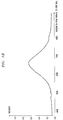
- the intensity within a collimated light beam transmitted through an etalon has the same intensity pattern as the incident beam, typically gaussian-like as shown in Fig. 1b.
- the incident and resonant light is diffracted, producing interference within the transmitted beam along the axis perpendicular to the step edge.
- the resulting fringe pattern is illustrated in Fig. 1c.
- the result of the diffraction is that in the vicinity of the step, there is substantial angular dispersion of the light which reduces the quality of the transmission function resulting in reduced signal amplitude, broadened peaks, as well as reduced ability.
- Fig. 1d Such an reduction in wavelength discrimination is illustrated in Fig. 1d for a two step etalon.
- Curves A1-A5 are measured on step A and curves B1-B5 are measured on step B.
- Curves A1 and B1 represent positions distant from the step transition.
- the remaining curves A2-A5 and B2-B5 are measurements made at locations progressively closer to the step transition.
- the input signal was provided by a temperature tuned laser and therefore increases in temperature represent increases in input signal wavelength.
- the peaks and troughs for curves close to the step transition lower and less defined than those measured far from the step transition, indicating that near the step transition, it is harder to discriminate between wavelengths that are close to each other.
- the size of the etalon can be increased to provide more area within each step land which is distant from the edge, this is often an undesirable solution.
- the detector array is commonly formed on an integrated circuit which may not be as easily increased in size without a relatively large increase in production cost.
- the width of the input light beam itself may not be variable and increasing the etalon width will introduce the additional problems of directing the beam to the desired portion of the etalon.
- a stepped etalon is formed where the transition between the lands of adjacent steps is "softened” or smoothed, i.e., non-abrupt, to thereby reduce diffraction banding, fringing, and other optical effects caused by the presence of sharp transition regions.
- Such softened or smoothed step transitions can be produced in several ways.
- the etalon steps can be formed by a directional "abrasive" etching process, such as reactive ion etching.
- the etching beam is applied to the etalon at an angle relative to the surface to be etched.
- the transition region between the resulting steps will have an angle substantially equal to the etch angle.
- Alternative fabrication techniques such as the use of an erodible photoresist mask in the region of the step transition, can also be used to produce a softer edge.
- preexisting abrupt or "hard” step transitions can be softened by post-processing techniques.
- the entire stepped surface of the etalon 30 is chemically etched. Because of the greater surface area and increased stresses associated with the step sharp corners, the corners will etch at a faster rate than the flat step lands, producing a softened transition region.
- the stepped region can be coated with a spin-on glass or other material, such as glass-laden epoxy, etc., which has an index of refraction similar to that of the etalon.
- the spin-on material forms a thin coating on the tops of the steps and a thicker coating in the step transitions regions. The coating thus fills in the abrupt inner corners and rounds the outer corners.
- the etalon is selectively annealed. Selective application of sufficient heat in the regions of the step transition to produce localized melting will produce a softened transition edge as the melted etalon glass flows and resolidifies.
- a stepped etalon in which the transition region between the lands of adjacent steps is not abrupt, but is instead "softened” or generally smoothed so as to reduce diffraction banding, fringing, and other optical effects caused by the presence of sharp transition regions.
- Softened or smoothed step transitions according to the invention can be produced in several ways, as are described below. Once steps with softened transition regions are formed, the stepped surface and the parallel opposing surface of the etalon are polished, if needed, to produce optically flat surfaces, and a partially reflective coating is applied, using techniques known to those of skill in the art, to form the completed etalon. Particular techniques for fabricating softened step etalons according to the invention are discussed below. It should be noted that while etalons having only two steps are discussed, the invention can be applied to etalons having any number of steps.
- a directional "abrasive" etching process such as reactive ion etching is used.
- Fig. 2a illustrates an etalon "blank" 20 comprised of a light transmitting material, such as SiO 2 glass.
- the blank 20 has a top surface 21 into which one or more steps are to be formed.
- a portion 26a of the surface 21 corresponding to the land of the highest step is coated with a layer of masking material 22, such as an appropriate photoresist or sacrificial material.
- a directed etching beam 24 is then applied to the etalon blank 20.
- the beam 24 is not applied normal to the surface 21, but instead is applied at an angle 25 which is less than 90 ⁇ relative to the surface 21.
- the portion 26a of the etalon surface 21 covered by the coating 22 is preserved. However, the exposed portion 26b of the surface 22 is etched. The etching depth depends on several factors, including the composition of the blank 20, the characteristics of the directed etching beam 24, and the duration of the etching process. Once the surface portion 26b is etched to the desired depth, the coating 22 is removed. Various techniques for coating and directional etching of an etalon blank will be known to those of skill in the art.
- the transition region 28 between the two steps is also angled.
- the angle of the transition region 28 between the protected portion 26a and the etched portion 26b will depend on the angle at which the etching beam 24 is applied. The smaller the angle, the less abrupt is the transition between the steps. However, as the angle is reduced, the width of the transition region 28 increases. Thus, the abruptness of the transition region is balanced with an increase in its width.
- the angle is selected to provide a non-abrupt transition region, i.e., resulting from a step transition having an angle less than approximately 75 ⁇ . In one embodiment, the angle is significantly less, preferably to provide a transition region which is between about 0.5 to 3 times the step height.
- an etalon with an abrupt step and having a height of approximately 2.0 um has a dead zone on the order of 600 to 800 um wide.
- a performance improvement can be obtained with a sloped transition region of width preferably up to about 400 um wide.
- the width of the transition region is between about 50 um and about 400 um.
- the etching beam is applied at a very shallow angle of between approximately 7 ⁇ and 0.3 ⁇ .
- the angle is preferably selected to be substantially equal to Brewster's angle (the angle at which all of the reflected ray is polarized) for the etalon material.
- this angle is approximately 38 ⁇ .
- narrower or significantly broader transition regions may be appropriate under various circumstances.
- softened transition steps are directly formed on an etalon blank by use of an erodible photoresist mask.
- an erodible mask is designed to erode at a known rate in a given etching environment. After the mask has eroded, erosion of the underlying substrate beings.
- the composition of the erodible mask is depending on the particular etching environment at issue and appropriate compositions will be known to those of skill in the art.
- various techniques are available for applying such an erodible mask, as will also be known to those of skill in the art.
- the resist can be applied with a "hard” edge and then reflowed after patterning by, .e.g., melting the resist or softening it with appropriate chemical agents.
- surface tension will provide for a softened edge in the form of a resist "tail” which extends past the masked edge approximately as far as the resist is high.
- the resist can be applied using "grey scale” printing techniques, wherein the edge of the resist is not abrupt, but instead is formed of a collection of resist "dots", spots, or other broken regions which become smaller and/or more widely spaced at distances further from the solid edge of the resist.
- the dots are configured such that the masking density, i.e., the average percentage of the etalon surface which is covered by the resist, drops across the transition region 28 from 100% over region 26a to 0% over region 26b.
- the grey scale resist dots can be reflowed to provide a solid resist layer with gradually reducing varying thicknesses, such as shown in Fig. 3a.
- Fig. 3a illustrates an etalon blank 20 having an erodible resist mask 30 applied over portion 26a of the etalon surface 21.
- the thickness of the mask 30 over portion 26a is preferably sufficient to survive the etching process. As illustrated, the mask thickness is reduced over the transition region 28 so that the mask has a sloped edge.
- the exposed portion 26b will begin to erode immediately.
- the transition region 28 will begin to erode as the overlying sloped mask erodes away and progressively exposes more of the underlying transition region.
- Fig. 3b illustrates the etalon 20 after etching, with the original surface 21 and mask area illustrated in broken line. As shown, the transition region 28 has a profile which corresponds generally to that of the original erodible mask 30. The remaining (non-eroded) portion of the mask 30' is then removed to provide an etalon similar to that shown in Fig. 2b.
- FIG. 4a Another embodiment of the invention begins with a partially fabricated conventional stepped etalon 40, such as shown in Fig. 4a.
- Surface 41 of the etalon 40 has step lands 42a and 42b which are separated by an abrupt transition region 44. Additional processing steps are applied to etalon blank to soften the transition region 44 between the steps.
- the entire stepped surface 41 of the etalon 40 is chemically etched with an appropriate etchant, such as buffered hydrofluoric acid.
- an appropriate etchant such as buffered hydrofluoric acid.
- the surface 41 of the stepped etalon 40 is coated with a spin-on glass or other material, such as glass-laden epoxy, etc.
- the coating has an index of refraction substantially equal to that of the etalon to avoid producing undesired diffraction at other places in the etalon.
- suitable coating materials will be known to those of skill in the art.
- An etalon 40 having such an applied additional layer 48 is shown in Fig. 4c.
- the spin-on material forms a thin coating on the majority of tops of the step lands 42a, 42b and a thicker coating in the step transitions region 44 and possibly adjacent areas of the step lands 42a, 42b.
- the thicker coating in the transition region 44 fills in the abrupt inner corners and rounds the outer corners and provides a softened transition 44'. If the coating does not cover the entire step lands, the application is preferably made in a manner which produces a smooth transition between the edge of the coating and the uncoated etalon surface to thereby avoid the introduction of additional steps on the etalon surface.
- the coating 48 can be deposited across the entire surface of the etalon using, e.g., plasma or epitaxial growth processes as shown in Fig. 4f.
- the coating can be of the same composition as the etalon since it does not need to flow, as is generally a requirement for spin-on application.
- a layer of SiO 2 can be deposited on top of a etalon comprised substantially of SiO 2 .
- the partially processed stepped etalon 40 is selectively annealed.
- heat sufficient to produced localized melting is selectively applied to the step transition regions.
- the localized melting produces a softened transition edge as the melted etalon glass flows and then resolidifies.
- Various techniques for selective annealing will be known to those of skill in the art, and include application of heat via directed laser beams.
- two or more laser beams are directed at the etalon so that they intersect at the transition region. The beam intensity is selected to that no single beam is of sufficient intensity to melt the etalon material, but that the combination of the beams introduces sufficient heat to produced localized melting where the beams intersect.
- the etalon 40 is treated not to reduce the abrupt transition between the steps, step, but instead to reduce the effect of abrupt transition. This is accomplished by masking the etalon surfaces 26a, 26b with a suitable material 47 while leaving the step transition region 44 exposed and then doping the etalon in the region of the step transition 44 with a dopant which absorbs the light in the frequency range of interest. Because of the mask 47, the dopant will only be implanted in a small region 49 surrounding the transition region 44.
- the dopant absorbs light that would otherwise be defracted, thus reducing the interference caused by an abrupt step.
- the dopant is implanted in a controlled manner which produces a non-abrupt doping gradient. There are many ways in which to produce such a gradual doping transition which will be known to those of skill in the art. This technique is particularly useful for fabrication of etalons which are to be used with generally monochromatic light, such as etalons used to tune lasers.
- an erbium dopant could be used in a stepped etalon which is used to detect light energy having a wavelength of approximately 980nm and the appropriate glass composition.
- Other dopants can be used, depending on the frequencies of light to be applied to the etalon and the etalon material.
- a combination of various dopants can be used to absorb a variety of different light frequencies.
- a stepped etalon having softened step transitions is produced, the stepped surface of the etalon and the surface opposing the steps is polished, if needed, to an optical flatness. Then, a partially reflecting coating is applied to the stepped and opposing surfaces using materials and techniques known to those of skill in the art.
- a softened step etalon 50 is illustrated in Fig. 5. As shown, the etalon 50 has an upper surface 51 comprising step lands 52a and 52b separated by a softened transition region 54. The etalon 50 has an opposing surface 56 which is preferably parallel to the step lands 52a, 52b. A partially reflective coating 58 covers surfaces 51 and 56.
- the transition region 54 between the steps is not abrupt, the optical interference produced by the step transition is reduced when compared to etalons having abrupt step transitions. This advantageously allows a greater portion of the light transmitted in the region of the steps to be used when determining transmitted light intensity, thereby providing a more sensitive device. Alternatively, for a given sensor size, the size of the etalon can be reduced. Other advantages will also be recognized by those of skill in the art.
Abstract
An improved stepped etalon comprises a transparent body having
a stepped surface. The lands of the steps are separated by a non-abrupt or
softened transition region. This reduces the diffraction of light caused by the
step transitions, thereby reducing the dead spot behind the step transition
portions where interference prevents accurate measurements of light
transmission from being made. Methods for producing a smoothly stepped
etalon and for smoothing the step transitions in an abruptly stepped etalon are
also disclosed.
Description
- This invention is related to an improved multi-wavelength stepped etalon.
- In many applications, it is necessary to accurately determine the wavelength(s) of light incident on a suitable detector. A widely used type of detector includes an etalon to filter specific frequencies of light. An etalon is a type of interference filter in which the intensity of transmitted light is dependent on its wavelength. In a conventional design, an etalon is comprised of two partially reflective parallel surfaces a distance d apart and separated by a material with an index of refraction r. When collimated light having a wavelength λ is passed through the etalon, some of the light is reflected from the surfaces. The multiply reflected light beams interfere, either constructively or destructively, with each other, and thus alter the overall intensity of the light which passes through the
etalon 10. Maximum transmission occurs when twice the distance between the reflective surfaces 12, 14 is an integral number of wavelengths λ in the etalon. In other words, - Often, it is desirable to provide a sensor which is sensitive to, and can discriminate among, several different frequencies of incident light at the same time. Such a sensor is particular useful for spectrographic analysis. Although several discrete etalons can be utilized for this purpose, in some implementations, a stepped etalon is used instead. In this arrangement, one or both active surfaces of the etalon are stepped so that each step on the etalon provides a region of different thickness. By adjusting the thicknesses appropriately, each step can be configured to pass different frequencies of light. Stepped spectrographic etalon arrangements of this type are shown in U.S. Patent No. 4,822,998 to Yokota et al. and U.S. Patent No. 5,144,498 to Vincent.
- A newly developed application is the use of a specifically configured stepped etalon to tune the output frequency of a laser. For fiber optic communications in particular, accurate tuning of the communication lasers is necessary to permit adjacent transmission channels to be closely spaced, often at wavelengths differing by only 0.4 nanometers or less. For such closely spaced channels, a laser's wavelength must be tuned to the assigned channel with an accuracy of +/- 0.1 nanometers or less. Although only a single wavelength of light needs to be detected to tune such a laser, at these high accuracies, thermal variations in the thickness of an etalon and slight variations in the angle of applied light from normal to the etalon surface can shift the light transfer function an unacceptable degree.
- According to the new application, the nominal thickness of the etalon can be chosen so that the periodicity of the etalon filter roughly matches the periodicity of a data communication channel spacing, i.e., 1500.12, 1550.52 nm for a system with a channel separation of substantially 0.4 nm. Two or more steps are formed on one side of the etalon. The step size is selected to be a fraction of the channel separation, on the order of 0.1 nm, and is substantially optimized so that a peak or trough in the transmission curve in the region of one step overlaps a steep portion of the transmission curve for one or more other steps. In this manner, as thermal changes in the etalon shift the transmission curve for one step beyond the desired range, the curve for a second step is shifted into the desired frequency. By selecting a particular step according to a measured temperature and etalon calibration information, and measuring the intensity of laser light transmitted through the selected step of the etalon, a feedback signal is provided which can be used to adjust the output wavelength of the laser. Similarly, different steps can be selected to compensate for tolerance errors in the angle of light incident the etalon. This configuration is more fully described in a co-pending patent application entitled "Controlled Multi-wavelength Etalon," filed concurrently with the present application and assigned to Lucent Technologies, Inc., and the entire contents of which is hereby incorporated by reference.
- With reference to Fig. 1a, in both types of stepped etalon configurations, the
stepped etalon 10 having partiallyreflective coatings photodetectors corresponding etalon step light 16 is directed onto theetalon 10, the intensity of the output signal attributed to eachdetector - A significant drawback to a conventional stepped etalon is the interference caused by the abrupt transition between the lands of adjacent steps. When no step is present, the intensity within a collimated light beam transmitted through an etalon has the same intensity pattern as the incident beam, typically gaussian-like as shown in Fig. 1b. However, when an abrupt step is present, the incident and resonant light is diffracted, producing interference within the transmitted beam along the axis perpendicular to the step edge. The resulting fringe pattern is illustrated in Fig. 1c. The result of the diffraction is that in the vicinity of the step, there is substantial angular dispersion of the light which reduces the quality of the transmission function resulting in reduced signal amplitude, broadened peaks, as well as reduced ability.
- Such an reduction in wavelength discrimination is illustrated in Fig. 1d for a two step etalon. Curves A1-A5 are measured on step A and curves B1-B5 are measured on step B. Curves A1 and B1 represent positions distant from the step transition. The remaining curves A2-A5 and B2-B5 are measurements made at locations progressively closer to the step transition. The input signal was provided by a temperature tuned laser and therefore increases in temperature represent increases in input signal wavelength. As indicated, the peaks and troughs for curves close to the step transition lower and less defined than those measured far from the step transition, indicating that near the step transition, it is harder to discriminate between wavelengths that are close to each other.
- The effect of the interference and overall reduction in etalon quality associated with abrupt steps creates a "dead spot" behind and near the step edge in which accurate intensity readings are compromised. Thus, there are portions of the etalon where a detector cannot be placed due to the reduced quality of the transmitted beam.
- For example, experiments using an etalon with a thickness of approximately 2mm and a step height of approximately 0.2 um reveal a "dead spot" approximately 600 to 800 um wide directly behind the step. Since input beam widths of between 0.5 to 5.0 mm are common, a significant portion of the transmitted beam will not have high quality etalon transmission characteristics and thus will not be suitable for detection. This reduces the available optical power for measurement and lowers the power-per-detector. Since a minimum signal-to-noise ratio is required for reliable measurements, decreasing the power-per-detector thus can decrease the accuracy of the detector and the stability of equipment which is adjusted according to the etalon measurements. The interference also limits the number of possible steps which can be placed on an etalon of a given size.
- Although the size of the etalon can be increased to provide more area within each step land which is distant from the edge, this is often an undesirable solution. First, the detector array is commonly formed on an integrated circuit which may not be as easily increased in size without a relatively large increase in production cost. Second, the width of the input light beam itself may not be variable and increasing the etalon width will introduce the additional problems of directing the beam to the desired portion of the etalon.
- According to the invention, a stepped etalon is formed where the transition between the lands of adjacent steps is "softened" or smoothed, i.e., non-abrupt, to thereby reduce diffraction banding, fringing, and other optical effects caused by the presence of sharp transition regions. Such softened or smoothed step transitions can be produced in several ways.
- During the step fabrication process, the etalon steps can be formed by a directional "abrasive" etching process, such as reactive ion etching. The etching beam is applied to the etalon at an angle relative to the surface to be etched. The transition region between the resulting steps will have an angle substantially equal to the etch angle. Alternative fabrication techniques, such as the use of an erodible photoresist mask in the region of the step transition, can also be used to produce a softer edge.
- Alternatively, preexisting abrupt or "hard" step transitions can be softened by post-processing techniques. In one method, the entire stepped surface of the
etalon 30 is chemically etched. Because of the greater surface area and increased stresses associated with the step sharp corners, the corners will etch at a faster rate than the flat step lands, producing a softened transition region. Alternatively, the stepped region can be coated with a spin-on glass or other material, such as glass-laden epoxy, etc., which has an index of refraction similar to that of the etalon. The spin-on material forms a thin coating on the tops of the steps and a thicker coating in the step transitions regions. The coating thus fills in the abrupt inner corners and rounds the outer corners. In yet another alternative, the etalon is selectively annealed. Selective application of sufficient heat in the regions of the step transition to produce localized melting will produce a softened transition edge as the melted etalon glass flows and resolidifies. - The foregoing and other features of the present invention will be more readily apparent from the following detailed description and drawings of illustrative embodiments of the invention in which:
- Fig. 1a is a representation of a conventional stepped etalon;
- Fig. 1b is a graph of the intensity of a light beam transmitted by an unstepped etalon;
- Fig. 1c is a graph of the intensity of a light beam transmitted by a stepped etalon and passing through the step transition region;
- Fig. 1d is a graph of the intensity of light beams transmitted by a stepped etalon measured at different lateral distances from the step;
- Figs. 2a and 2b illustrate the production of a softened step etalon by directed etching;
- Figs. 3a and 3b illustrate the production of a softened step etalon by use of an erodible mask;
- Fig. 4a is an illustration of a partially fabricated etalon having abrupt step transitions;
- Figs. 4b-4e illustrate methods of processing the etalon of Fig. 4a to provide softened step transitions; and
- Fig. 5 is an illustration of a softened stepped etalon according to the invention.
-
- According to the invention, a stepped etalon is provided in which the transition region between the lands of adjacent steps is not abrupt, but is instead "softened" or generally smoothed so as to reduce diffraction banding, fringing, and other optical effects caused by the presence of sharp transition regions. Softened or smoothed step transitions according to the invention can be produced in several ways, as are described below. Once steps with softened transition regions are formed, the stepped surface and the parallel opposing surface of the etalon are polished, if needed, to produce optically flat surfaces, and a partially reflective coating is applied, using techniques known to those of skill in the art, to form the completed etalon. Particular techniques for fabricating softened step etalons according to the invention are discussed below. It should be noted that while etalons having only two steps are discussed, the invention can be applied to etalons having any number of steps.
- According to a first embodiment of the invention, softened transition etalon steps are directly formed in an etalon blank. In one technique, a directional "abrasive" etching process, such as reactive ion etching is used. Fig. 2a illustrates an etalon "blank" 20 comprised of a light transmitting material, such as SiO2 glass. The blank 20 has a
top surface 21 into which one or more steps are to be formed. Aportion 26a of thesurface 21 corresponding to the land of the highest step is coated with a layer of maskingmaterial 22, such as an appropriate photoresist or sacrificial material. A directedetching beam 24 is then applied to theetalon blank 20. According to an embodiment of the invention, thebeam 24 is not applied normal to thesurface 21, but instead is applied at anangle 25 which is less than 90□ relative to thesurface 21. - The
portion 26a of theetalon surface 21 covered by thecoating 22 is preserved. However, the exposedportion 26b of thesurface 22 is etched. The etching depth depends on several factors, including the composition of the blank 20, the characteristics of the directedetching beam 24, and the duration of the etching process. Once thesurface portion 26b is etched to the desired depth, thecoating 22 is removed. Various techniques for coating and directional etching of an etalon blank will be known to those of skill in the art. - Because the
etching beam 24 is applied at an angle, thetransition region 28 between the two steps is also angled. As can be appreciated, the angle of thetransition region 28 between the protectedportion 26a and the etchedportion 26b will depend on the angle at which theetching beam 24 is applied. The smaller the angle, the less abrupt is the transition between the steps. However, as the angle is reduced, the width of thetransition region 28 increases. Thus, the abruptness of the transition region is balanced with an increase in its width. According to the invention, the angle is selected to provide a non-abrupt transition region, i.e., resulting from a step transition having an angle less than approximately 75□. In one embodiment, the angle is significantly less, preferably to provide a transition region which is between about 0.5 to 3 times the step height. - For example, an etalon with an abrupt step and having a height of approximately 2.0 um has a dead zone on the order of 600 to 800 um wide. A performance improvement can be obtained with a sloped transition region of width preferably up to about 400 um wide. Most preferably, for this step configuration, the width of the transition region is between about 50 um and about 400 um. To produce a transition region of this width, the etching beam is applied at a very shallow angle of between approximately 7□ and 0.3□.
- In another embodiment, providing a shorter non-abrupt transition region, the angle is preferably selected to be substantially equal to Brewster's angle (the angle at which all of the reflected ray is polarized) for the etalon material. For glass, this angle is approximately 38□. However, narrower or significantly broader transition regions may be appropriate under various circumstances.
- According to another technique, softened transition steps are directly formed on an etalon blank by use of an erodible photoresist mask. Unlike traditional photoresist masking materials, an erodible mask is designed to erode at a known rate in a given etching environment. After the mask has eroded, erosion of the underlying substrate beings. By varying the thickness of the erodible mask, different areas of the substrate will be exposed to the etching environment at different times, and thus will be etched to different depths. The composition of the erodible mask is depending on the particular etching environment at issue and appropriate compositions will be known to those of skill in the art. In addition, various techniques are available for applying such an erodible mask, as will also be known to those of skill in the art.
- For example, the resist can be applied with a "hard" edge and then reflowed after patterning by, .e.g., melting the resist or softening it with appropriate chemical agents. Generally, surface tension will provide for a softened edge in the form of a resist "tail" which extends past the masked edge approximately as far as the resist is high. To provide a longer tail, the resist can be applied using "grey scale" printing techniques, wherein the edge of the resist is not abrupt, but instead is formed of a collection of resist "dots", spots, or other broken regions which become smaller and/or more widely spaced at distances further from the solid edge of the resist. The dots are configured such that the masking density, i.e., the average percentage of the etalon surface which is covered by the resist, drops across the
transition region 28 from 100% overregion 26a to 0% overregion 26b. After application, the grey scale resist dots can be reflowed to provide a solid resist layer with gradually reducing varying thicknesses, such as shown in Fig. 3a. - Fig. 3a illustrates an etalon blank 20 having an erodible resist
mask 30 applied overportion 26a of theetalon surface 21. The thickness of themask 30 overportion 26a is preferably sufficient to survive the etching process. As illustrated, the mask thickness is reduced over thetransition region 28 so that the mask has a sloped edge. When theetalon 20 is placed in a suitable etching environment, the exposedportion 26b will begin to erode immediately. Thetransition region 28 will begin to erode as the overlying sloped mask erodes away and progressively exposes more of the underlying transition region. - Fig. 3b illustrates the
etalon 20 after etching, with theoriginal surface 21 and mask area illustrated in broken line. As shown, thetransition region 28 has a profile which corresponds generally to that of the originalerodible mask 30. The remaining (non-eroded) portion of the mask 30' is then removed to provide an etalon similar to that shown in Fig. 2b. - Another embodiment of the invention begins with a partially fabricated conventional stepped
etalon 40, such as shown in Fig. 4a.Surface 41 of theetalon 40 has step lands 42a and 42b which are separated by anabrupt transition region 44. Additional processing steps are applied to etalon blank to soften thetransition region 44 between the steps. - In a first method for this embodiment, the entire stepped
surface 41 of theetalon 40 is chemically etched with an appropriate etchant, such as buffered hydrofluoric acid. Although the entire exposed surface of the etalon will be etched to some degree, the corners will etch at a faster rate than the flat step lands because there are increased material stresses associated with sharp step corners and also because the corners have a greater surface area exposed to the etching environment. The difference in etching rates softens the transition region. Fig. 4b illustratesetalon 40 after such a chemical etching process has been applied. The material 46 removed by the additional etching is illustrated in broken lines - In a second method, the
surface 41 of the steppedetalon 40 is coated with a spin-on glass or other material, such as glass-laden epoxy, etc. Preferably, the coating has an index of refraction substantially equal to that of the etalon to avoid producing undesired diffraction at other places in the etalon. Various suitable coating materials will be known to those of skill in the art. Anetalon 40 having such an appliedadditional layer 48 is shown in Fig. 4c. The spin-on material forms a thin coating on the majority of tops of the step lands 42a, 42b and a thicker coating in the step transitionsregion 44 and possibly adjacent areas of the step lands 42a, 42b. The thicker coating in thetransition region 44 fills in the abrupt inner corners and rounds the outer corners and provides a softened transition 44'. If the coating does not cover the entire step lands, the application is preferably made in a manner which produces a smooth transition between the edge of the coating and the uncoated etalon surface to thereby avoid the introduction of additional steps on the etalon surface. - In a variant of the spin-on method, the
coating 48 can be deposited across the entire surface of the etalon using, e.g., plasma or epitaxial growth processes as shown in Fig. 4f. In such an arrangement the coating can be of the same composition as the etalon since it does not need to flow, as is generally a requirement for spin-on application. For example, a layer of SiO2 can be deposited on top of a etalon comprised substantially of SiO2. - In yet another alternative, the partially processed stepped
etalon 40 is selectively annealed. In particular, heat sufficient to produced localized melting is selectively applied to the step transition regions. The localized melting produces a softened transition edge as the melted etalon glass flows and then resolidifies. Various techniques for selective annealing will be known to those of skill in the art, and include application of heat via directed laser beams. In one embodiment, two or more laser beams are directed at the etalon so that they intersect at the transition region. The beam intensity is selected to that no single beam is of sufficient intensity to melt the etalon material, but that the combination of the beams introduces sufficient heat to produced localized melting where the beams intersect. - In a further embodiment, illustrated in Fig. 4e, the
etalon 40 is treated not to reduce the abrupt transition between the steps, step, but instead to reduce the effect of abrupt transition. This is accomplished by masking theetalon surfaces step transition region 44 exposed and then doping the etalon in the region of thestep transition 44 with a dopant which absorbs the light in the frequency range of interest. Because of the mask 47, the dopant will only be implanted in asmall region 49 surrounding thetransition region 44. - The dopant absorbs light that would otherwise be defracted, thus reducing the interference caused by an abrupt step. The dopant is implanted in a controlled manner which produces a non-abrupt doping gradient. There are many ways in which to produce such a gradual doping transition which will be known to those of skill in the art. This technique is particularly useful for fabrication of etalons which are to be used with generally monochromatic light, such as etalons used to tune lasers.
- For example, in a stepped etalon which is used to detect light energy having a wavelength of approximately 980nm and the appropriate glass composition, an erbium dopant could be used. Other dopants can be used, depending on the frequencies of light to be applied to the etalon and the etalon material. In addition, a combination of various dopants can be used to absorb a variety of different light frequencies.
- As discussed above, once a stepped etalon having softened step transitions is produced, the stepped surface of the etalon and the surface opposing the steps is polished, if needed, to an optical flatness. Then, a partially reflecting coating is applied to the stepped and opposing surfaces using materials and techniques known to those of skill in the art. Such a
softened step etalon 50 is illustrated in Fig. 5. As shown, theetalon 50 has anupper surface 51 comprising step lands 52a and 52b separated by a softenedtransition region 54. Theetalon 50 has an opposingsurface 56 which is preferably parallel to the step lands 52a, 52b. A partiallyreflective coating 58 covers surfaces 51 and 56. - Because the
transition region 54 between the steps is not abrupt, the optical interference produced by the step transition is reduced when compared to etalons having abrupt step transitions. This advantageously allows a greater portion of the light transmitted in the region of the steps to be used when determining transmitted light intensity, thereby providing a more sensitive device. Alternatively, for a given sensor size, the size of the etalon can be reduced. Other advantages will also be recognized by those of skill in the art. - While the invention has been particularly shown and described with reference to preferred embodiments thereof, it will be understood by those skilled in the art that various changes in form and details may be made therein without departing from the scope of the invention. In particular, the various processing steps disclosed above do not need to be used in isolation, but instead can be combined as desired. For example, an etalon can be fabricated using directed etching as shown in Figs. 2a and the resulting softened stepped etalon, shown in Fig. 2b, and then a spin-on glass coating can be applied, such as illustrated in Fig. 4, to further soften the transition. Other combinations of processing steps are also possible.
Claims (17)
- A stepped etalon comprising:a body which is transparent at least in a predetermined range of wavelengths and having first and second opposing sides;the first side having a surface;the second side having a plurality of steps, each step having a land substantially parallel to the surface,the lands of adjacent steps being separated by a non-abrupt transition region.
- A stepped etalon comprising:a body which is transparent at least in a predetermined range of wavelengths and having first and second opposing sides;the first side having a surface;the second side having a plurality of steps, each step having a land substantially parallel to the surface,the lands of adjacent steps being separated by a transition region;a coating substantially transparent to light having a wavelength within said predetermined range applied over said steps and transition regions;
wherein said coating smooths the transition region between lands of adjacent steps. - The stepped etalon of claim 2, wherein:the body has a predetermined index of refraction;said coating having an index of refraction substantially equal to said predetermined index of refraction.
- A stepped etalon comprising:a body which is transparent at least in a first range of wavelengths and having first and second opposing sides;the first side having a surface;the second side having a plurality of steps, each step having a land substantially parallel to the surface,the lands of adjacent steps being separated by a transition region;the body having a light-absorbing dopant implanted in said transition regions, said dopant absorbing light having a wavelength within said predetermined range.
- The etalon of claim 4, wherein said dopant comprises erbium.
- A method of producing a stepped etalon having softened step transitions comprising the steps of:providing an etalon body which is transparent at least in a first range of wavelengths and having first and second opposing sides;depositing a masking material over a first portion of said first side while leaving a second portion of said first side exposed;applying a directional abrasive etching beam to said first side at an angle less than ninety degrees relative to said first side for a predetermined amount of time; andremoving said masking material.
- A method of producing a stepped etalon having softened step transitions comprising the steps of:providing an etalon body which is transparent at least in a first range of wavelengths and having first and second opposing sides;depositing an erodible masking material of a predetermined thickness over a first portion of said first side while leaving a second portion of said first side exposed, the first and second portions being separated by a transition region, the masking material having a tail region of gradually decreasing thickness over the transition region;etching said first side and erodible masking material for a predetermined amount of time; andremoving any remaining masking material from the first side.
- The method of claim 7, wherein the step of depositing comprises the steps of:depositing said masking material over the first portion while leaving said transition region and said second portion exposed; andreflowing said masking material a sufficient degree for the masking material to flow over said transition region.
- The method of claim 7, wherein the step of depositing comprises the steps of:depositing said masking material over the first portion in a solid layer having said predetermined thickness; anddepositing said masking material over the transition region using grey scale techniques to provide an average masking density which drops to zero across the transition region from the first portion to the second portion.
- The method of claim 9, further comprising the steps of reflowing the masking material on the transition region.
- A method of producing a stepped etalon having softened step transitions comprising the steps of:providing an etalon body which is transparent at least in a first range of wavelengths and having first and second opposing sides, said first side having a plurality of steps, adjacent steps separated by a generally abrupt transition region; andfurther processing the etalon body to soften the abrupt nature of the transition region.
- The method of claim 11, wherein the step of further processing comprises the step of chemically etching the first side of the etalon.
- The method of claim 11, wherein the step of further processing comprises the step of applying to the first side of the etalon a coating which is substantially transparent to light having a wavelength within said predetermined range.
- The method of claim 13, wherein said etalon body has a predetermined index of refraction and said coating has an index of refraction substantially equal to said predetermined index of refraction.
- The method of claim 11, wherein the step of further processing comprises the step of selectively annealing at least the transition regions between said steps.
- A method of producing an etalon having a step transition with a reduced degree of unwanted interference comprising the steps of:providing an etalon body which is transparent at least in a first range of wavelengths and having first and second opposing sides, said first side having a plurality of steps, adjacent steps separated by a generally abrupt transition region;masking the steps on the first side of the etalon body while leaving the transition region substantially exposed; anddoping the exposed transition region with a light-absorbing dopant, said dopant absorbing light having a wavelength within said predetermined range.
- The method of claim 16, wherein the step of doping comprises the step of doping the exposed transition region with erbium.
Applications Claiming Priority (2)
| Application Number | Priority Date | Filing Date | Title |
|---|---|---|---|
| US09/312,386 US6500521B2 (en) | 1999-05-14 | 1999-05-14 | Stepped etalon |
| US312386 | 1999-05-14 |
Publications (1)
| Publication Number | Publication Date |
|---|---|
| EP1052484A2 true EP1052484A2 (en) | 2000-11-15 |
Family
ID=23211206
Family Applications (1)
| Application Number | Title | Priority Date | Filing Date |
|---|---|---|---|
| EP00303992A Withdrawn EP1052484A2 (en) | 1999-05-14 | 2000-05-11 | Improved stepped etalon |
Country Status (3)
| Country | Link |
|---|---|
| US (2) | US6500521B2 (en) |
| EP (1) | EP1052484A2 (en) |
| JP (1) | JP2001004827A (en) |
Cited By (3)
| Publication number | Priority date | Publication date | Assignee | Title |
|---|---|---|---|---|
| US6339603B1 (en) | 2000-10-25 | 2002-01-15 | Axsun Technologies, Inc. | Tunable laser with polarization anisotropic amplifier for fabry-perot filter reflection isolation |
| US6549548B2 (en) | 2000-10-25 | 2003-04-15 | Axsun Technologies, Inc. | Interferometric filter wavelength meter and controller |
| WO2014074254A1 (en) * | 2012-10-08 | 2014-05-15 | Si-Ware Systems | Fourier transform micro spectrometer based on spatially-shifted interferogram bursts |
Families Citing this family (14)
| Publication number | Priority date | Publication date | Assignee | Title |
|---|---|---|---|---|
| US7187447B1 (en) * | 2000-03-30 | 2007-03-06 | Lucent Technologies Inc. | Fabry-perot stepped etalon with improved transmittance characteristics |
| JP2002251793A (en) * | 2001-02-21 | 2002-09-06 | Sony Corp | Manufacturing method for master disk of optical recording medium |
| DE60100469T2 (en) * | 2001-10-22 | 2004-06-09 | Agilent Technologies, Inc. (n.d.Ges.d.Staates Delaware), Palo Alto | Wavelength meter with increased accuracy in a wide range of wavelengths |
| US8546082B2 (en) * | 2003-09-11 | 2013-10-01 | Ibis Biosciences, Inc. | Methods for identification of sepsis-causing bacteria |
| US8097416B2 (en) | 2003-09-11 | 2012-01-17 | Ibis Biosciences, Inc. | Methods for identification of sepsis-causing bacteria |
| US20120122096A1 (en) | 2003-09-11 | 2012-05-17 | Rangarajan Sampath | Compositions for use in identification of bacteria |
| NO322438B1 (en) * | 2005-04-15 | 2006-10-02 | Sinvent As | Adjustable interference filter |
| NO322368B1 (en) * | 2005-04-15 | 2006-09-25 | Sinvent As | Infrared gas detection - diffractive. |
| US20080264553A1 (en) * | 2007-04-27 | 2008-10-30 | Hewlett-Packard Development Company Lp | Embossing |
| JP2015149366A (en) * | 2014-02-05 | 2015-08-20 | キヤノン株式会社 | Semiconductor device manufacturing method |
| KR101624717B1 (en) * | 2014-12-24 | 2016-05-26 | 주식회사 토비스 | a delay etched member and a etching method of display panel using the same |
| WO2020113147A1 (en) * | 2018-11-29 | 2020-06-04 | Rydberg Technologies Inc. | A waveguide etalon |
| CN113692298B (en) | 2019-04-17 | 2024-02-13 | 巴德阿克塞斯系统股份有限公司 | Catheter securement devices including extended anchor pad and release liner snap-fit features |
| US11227790B1 (en) * | 2019-06-11 | 2022-01-18 | Ciena Corporation | Managing trench depth in integrated systems |
Family Cites Families (10)
| Publication number | Priority date | Publication date | Assignee | Title |
|---|---|---|---|---|
| US2769111A (en) * | 1951-07-25 | 1956-10-30 | Philco Corp | Optical system |
| US4822998A (en) | 1986-05-15 | 1989-04-18 | Minolta Camera Kabushiki Kaisha | Spectral sensor with interference filter |
| US5144498A (en) | 1990-02-14 | 1992-09-01 | Hewlett-Packard Company | Variable wavelength light filter and sensor system |
| EP0461042B1 (en) * | 1990-06-06 | 1995-08-23 | Fujitsu Limited | High speed optosemiconductor device having multiple quantum wells |
| US5128798A (en) | 1991-02-07 | 1992-07-07 | International Business Machines Corporation | Addressable wedge etalon filter |
| US5784507A (en) * | 1991-04-05 | 1998-07-21 | Holm-Kennedy; James W. | Integrated optical wavelength discrimination devices and methods for fabricating same |
| US5289314A (en) * | 1992-03-25 | 1994-02-22 | Hughes Aircraft Company | Coatings for laser detector etalons |
| US5293548A (en) * | 1992-03-25 | 1994-03-08 | Hughes Aircraft Company | Dispersive rugate coatings |
| DE69615721T2 (en) * | 1995-03-17 | 2002-08-08 | Ebara Corp | Manufacturing process with a bundle of energy |
| US6323987B1 (en) * | 1999-05-14 | 2001-11-27 | Agere Systems Optoelectronics Guardian Corp. | Controlled multi-wavelength etalon |
-
1999
- 1999-05-14 US US09/312,386 patent/US6500521B2/en not_active Expired - Lifetime
-
2000
- 2000-05-11 EP EP00303992A patent/EP1052484A2/en not_active Withdrawn
- 2000-05-15 JP JP2000142471A patent/JP2001004827A/en active Pending
-
2001
- 2001-08-21 US US09/934,283 patent/US6926841B2/en not_active Expired - Fee Related
Cited By (5)
| Publication number | Priority date | Publication date | Assignee | Title |
|---|---|---|---|---|
| US6339603B1 (en) | 2000-10-25 | 2002-01-15 | Axsun Technologies, Inc. | Tunable laser with polarization anisotropic amplifier for fabry-perot filter reflection isolation |
| US6549548B2 (en) | 2000-10-25 | 2003-04-15 | Axsun Technologies, Inc. | Interferometric filter wavelength meter and controller |
| US7095776B2 (en) | 2000-10-25 | 2006-08-22 | Axsun Technologies, Inc. | Interferometric filter wavelength meter and controller |
| WO2014074254A1 (en) * | 2012-10-08 | 2014-05-15 | Si-Ware Systems | Fourier transform micro spectrometer based on spatially-shifted interferogram bursts |
| US9429474B2 (en) | 2012-10-08 | 2016-08-30 | Si-Ware Systems | Fourier transform micro spectrometer based on spatially-shifted interferogram bursts |
Also Published As
| Publication number | Publication date |
|---|---|
| US20020150728A1 (en) | 2002-10-17 |
| US6500521B2 (en) | 2002-12-31 |
| JP2001004827A (en) | 2001-01-12 |
| US20020001331A1 (en) | 2002-01-03 |
| US6926841B2 (en) | 2005-08-09 |
Similar Documents
| Publication | Publication Date | Title |
|---|---|---|
| US6926841B2 (en) | Stepped etalon | |
| US6323987B1 (en) | Controlled multi-wavelength etalon | |
| EP0585094B1 (en) | An optical integrated circuit having light detector | |
| EP0461991B1 (en) | Spatial optical integrated monomode filter and method of manufacture | |
| US7412133B2 (en) | Wavelength selective optical focusing device using optical fiber and optical module using the same | |
| US6700664B1 (en) | Optical channel monitoring device | |
| US6246480B1 (en) | Stepped etalon | |
| US6778737B2 (en) | Optical waveguide with spot size changing core structure and method for manufacturing the same | |
| US7146074B2 (en) | Optical grating coupler | |
| US20060127819A1 (en) | Method for producing optical fiber | |
| US7672559B2 (en) | Optical waveguide device and fabricating method thereof | |
| EP0903596B1 (en) | Method of forming integrated optical circuit planar waveguide turning mirrors | |
| EP1591810A1 (en) | Grating apodization technique for diffused optical waveguides | |
| US5978532A (en) | Spectrographic multiplexer component having an array of waveguides | |
| US6650479B2 (en) | Multi-wavelength etalon | |
| JP2004523764A (en) | Integrated spectrometer with high spectral resolution, especially for high-speed communication and high-speed measurement, and method of manufacturing the same | |
| EP1402564B1 (en) | Integrated optical/electronic circuits and associated methods of simultaneous generation thereof | |
| CN103959116A (en) | Resonator optimization | |
| US10522975B2 (en) | Increasing accuracy in the wavelength of semiconductor lasers | |
| KR20070035913A (en) | Device for wavelength selective optical beam focusing using optical fiber and optical module unsing it | |
| Liu et al. | Hybrid optoelectronic digitally tunable receiver | |
| Peters et al. | Integrated optical devices with silicon oxynitride prepared by plasma-enhanced chemical vapor deposition (PECVD) on Si and GaAs substrates | |
| CA1298724C (en) | Reflectivity mirrors and transversely variable transmission apertures with an azimuthal symmetry | |
| Cohen et al. | SOI-based monolithic integration of SiON and Si planar optical circuits |
Legal Events
| Date | Code | Title | Description |
|---|---|---|---|
| PUAI | Public reference made under article 153(3) epc to a published international application that has entered the european phase |
Free format text: ORIGINAL CODE: 0009012 |
|
| AK | Designated contracting states |
Kind code of ref document: A2 Designated state(s): AT BE CH CY DE DK ES FI FR GB GR IE IT LI LU MC NL PT SE |
|
| AX | Request for extension of the european patent |
Free format text: AL;LT;LV;MK;RO;SI |
|
| STAA | Information on the status of an ep patent application or granted ep patent |
Free format text: STATUS: THE APPLICATION IS DEEMED TO BE WITHDRAWN |
|
| RIC1 | Information provided on ipc code assigned before grant |
Ipc: 7G 01J 3/26 A Ipc: 7G 02B 5/28 B |
|
| 18D | Application deemed to be withdrawn |
Effective date: 20021203 |