EP1052661A2 - Metal complex dye for a photoelectrochemical cell - Google Patents
Metal complex dye for a photoelectrochemical cell Download PDFInfo
- Publication number
- EP1052661A2 EP1052661A2 EP00110055A EP00110055A EP1052661A2 EP 1052661 A2 EP1052661 A2 EP 1052661A2 EP 00110055 A EP00110055 A EP 00110055A EP 00110055 A EP00110055 A EP 00110055A EP 1052661 A2 EP1052661 A2 EP 1052661A2
- Authority
- EP
- European Patent Office
- Prior art keywords
- group
- independently represent
- ring
- integer
- photoelectric conversion
- Prior art date
- Legal status (The legal status is an assumption and is not a legal conclusion. Google has not performed a legal analysis and makes no representation as to the accuracy of the status listed.)
- Granted
Links
- 0 CC(C=CN)I* Chemical compound CC(C=CN)I* 0.000 description 1
- RCMYNTKEGGWGTQ-UHFFFAOYSA-N CCC(C)C(N)[IH]C Chemical compound CCC(C)C(N)[IH]C RCMYNTKEGGWGTQ-UHFFFAOYSA-N 0.000 description 1
Images


Classifications
-
- C—CHEMISTRY; METALLURGY
- C09—DYES; PAINTS; POLISHES; NATURAL RESINS; ADHESIVES; COMPOSITIONS NOT OTHERWISE PROVIDED FOR; APPLICATIONS OF MATERIALS NOT OTHERWISE PROVIDED FOR
- C09B—ORGANIC DYES OR CLOSELY-RELATED COMPOUNDS FOR PRODUCING DYES, e.g. PIGMENTS; MORDANTS; LAKES
- C09B57/00—Other synthetic dyes of known constitution
- C09B57/10—Metal complexes of organic compounds not being dyes in uncomplexed form
-
- C—CHEMISTRY; METALLURGY
- C09—DYES; PAINTS; POLISHES; NATURAL RESINS; ADHESIVES; COMPOSITIONS NOT OTHERWISE PROVIDED FOR; APPLICATIONS OF MATERIALS NOT OTHERWISE PROVIDED FOR
- C09B—ORGANIC DYES OR CLOSELY-RELATED COMPOUNDS FOR PRODUCING DYES, e.g. PIGMENTS; MORDANTS; LAKES
- C09B57/00—Other synthetic dyes of known constitution
-
- H—ELECTRICITY
- H10—SEMICONDUCTOR DEVICES; ELECTRIC SOLID-STATE DEVICES NOT OTHERWISE PROVIDED FOR
- H10K—ORGANIC ELECTRIC SOLID-STATE DEVICES
- H10K85/00—Organic materials used in the body or electrodes of devices covered by this subclass
- H10K85/30—Coordination compounds
- H10K85/341—Transition metal complexes, e.g. Ru(II)polypyridine complexes
- H10K85/344—Transition metal complexes, e.g. Ru(II)polypyridine complexes comprising ruthenium
-
- H—ELECTRICITY
- H10—SEMICONDUCTOR DEVICES; ELECTRIC SOLID-STATE DEVICES NOT OTHERWISE PROVIDED FOR
- H10K—ORGANIC ELECTRIC SOLID-STATE DEVICES
- H10K85/00—Organic materials used in the body or electrodes of devices covered by this subclass
- H10K85/30—Coordination compounds
- H10K85/361—Polynuclear complexes, i.e. complexes comprising two or more metal centers
-
- H—ELECTRICITY
- H01—ELECTRIC ELEMENTS
- H01G—CAPACITORS; CAPACITORS, RECTIFIERS, DETECTORS, SWITCHING DEVICES OR LIGHT-SENSITIVE DEVICES, OF THE ELECTROLYTIC TYPE
- H01G9/00—Electrolytic capacitors, rectifiers, detectors, switching devices, light-sensitive or temperature-sensitive devices; Processes of their manufacture
- H01G9/20—Light-sensitive devices
- H01G9/2027—Light-sensitive devices comprising an oxide semiconductor electrode
- H01G9/2031—Light-sensitive devices comprising an oxide semiconductor electrode comprising titanium oxide, e.g. TiO2
-
- H—ELECTRICITY
- H01—ELECTRIC ELEMENTS
- H01G—CAPACITORS; CAPACITORS, RECTIFIERS, DETECTORS, SWITCHING DEVICES OR LIGHT-SENSITIVE DEVICES, OF THE ELECTROLYTIC TYPE
- H01G9/00—Electrolytic capacitors, rectifiers, detectors, switching devices, light-sensitive or temperature-sensitive devices; Processes of their manufacture
- H01G9/20—Light-sensitive devices
- H01G9/2059—Light-sensitive devices comprising an organic dye as the active light absorbing material, e.g. adsorbed on an electrode or dissolved in solution
-
- H—ELECTRICITY
- H01—ELECTRIC ELEMENTS
- H01G—CAPACITORS; CAPACITORS, RECTIFIERS, DETECTORS, SWITCHING DEVICES OR LIGHT-SENSITIVE DEVICES, OF THE ELECTROLYTIC TYPE
- H01G9/00—Electrolytic capacitors, rectifiers, detectors, switching devices, light-sensitive or temperature-sensitive devices; Processes of their manufacture
- H01G9/20—Light-sensitive devices
- H01G9/2068—Panels or arrays of photoelectrochemical cells, e.g. photovoltaic modules based on photoelectrochemical cells
- H01G9/2081—Serial interconnection of cells
Definitions
- the present invention relates to a metal complex dye, a photoelectric conversion device comprising semiconductor particles sensitized by the metal complex dye, and a photoelectric cell comprising the photoelectric conversion device.
- Solar cells for the solar power generation comprising a monocrystalline silicon, a polycrystalline silicon, an amorphous silicon, cadmium telluride, indium copper selenide, etc. have been the subject of practical use and a major object of research and development.
- problems for a widespread use of the solar cell as a home power source, etc., there are such problems as a high production cost, difficulty in security of raw materials, and a long energy payback time, therefore, these obstacles must be overcome.
- a variety of solar cells comprising organic materials are proposed with the objects of increasing the surface area of the cell, lowering the price thereof, etc. However, they generally have such defects as a low conversion efficiency and a poor durability.
- ruthenium complex dyes are disadvantageous in hardly absorbing an infrared ray with a wavelength of 700 nm or more. Consequently, a photoelectric conversion device comprising such a dye exhibits a low photoelectric conversion efficiency at infrared region. It has been desired to develop a dye having a high absorbancy at a large wave range containing visible region to infrared region.
- An object of the present invention is to provide a metal complex dye having a high absorbability not only at visible region but also at infrared region, which is able to efficiently sensitize semiconductor particles, a photoelectric conversion device comprising the metal complex dye which exhibits an excellent photoelectric conversion efficiency, and a photoelectric cell comprising the photoelectric conversion device.
- a metal complex dye comprising two or more metal atoms, a ligand having two or more moieties for bidentate or tridentate coordination to the metal atoms, and optional bidentate or tridentate ligand having nitrogen atoms for coordinating to the metal atom and monodentate or bidentate ligand(s) which coordinates to the metal atom via a dithiocarbamate group, a thiocyanate group, etc.
- the present invention has a high absorbancy in not only at visible region but also at long wavelength region and can efficiently sensitize semiconductor particles, and that a photoelectric conversion device comprising the metal complex dye exhibits an excellent photoelectric conversion efficiency, so that it is useful for a photoelectric cell.
- the present invention has been accomplished by the findings.
- the present invention provides the photoelectric conversion device comprising semiconductor particles sensitized by the metal complex dye represented by the following general formula (I): (LL 1 ) m1 (X 1 ) m2 M 1 (BL)M 2 (LL 2 ) m3 (X 2 ) m4 ⁇ CI wherein M 1 and M 2 independently represent a metal atom;
- the photoelectric cell of the present invention is characterized by the use of the photoelectric conversion device.
- the absorbancy at the long wavelength region and the photoelectric conversion efficiency are further improved by satisfying at least one of the following conditions (1) to (23).
- M 1 and M 2 independently represent a metal atom that is able to form four- or six-coordinated complex;
- BL represents a ligand having two or more moieties for bidentate coordination to the metal atoms, represented by any one of the general formulae B-1 to B-10;
- LL 1 and LL 2 independently represent a bidentate ligand represented by the general formulae (IV-1) or (IV-6);
- X 1 and X 2 independently represent a monodentate or bidentate ligand which coordinates to said metal atom via one or two groups selected from the group consisting of an acyloxy group, an acylthio group, a thioacyloxy group, a thioacylthio group, an acylaminooxy group, a thiocarbamate group, a dithiocarbamate group, a thiocarbonate group, a dithiocarbonate group, a tri
- M 1 and M 2 are Ru
- BL is represented by any one of the general formulae B-1 to B-4
- X 1 and X 2 independently represent a monodentate or bidentate ligand which coordinates to Ru via one or two groups selected from the group consisting of an acyloxy group, an acylaminooxy group, a dithiocarbamate group, a thiocyanate group, an isothiocyanate group, a cyanate group, an isocyanate group, an alkylthio group and an arylthio group.
- M 1 and M 2 are Ru;
- BL represents a ligand having two or more moieties for tridentate coordination to Ru, represented by any one of the general formulae B-12 to B-15;
- LL 1 and LL 2 independently represent a bidentate or tridentate ligand represented by any one of the general formulae (IV-1) to (IV-8);
- X 1 and X 2 independently represent a monodentate or bidentate ligand which coordinates to Ru via one or two groups selected from the group consisting of an acyloxy group, an acylthio group, a thioacyloxy group, a thioacylthio group, an acylaminooxy group, a thiocarbamate group, a dithiocarbamate group, a thiocarbonate group, a dithiocarbonate group, a trithiocarbonate group, an acyl group, a thiocyanate group,
- a metal complex dye for use in a photoelectric conversion device of the present invention is represented by the following general formula (I).
- (LL 1 ) m1 (X 1 ) m2 M 1 (BL)M 2 (LL 2 ) m3 (X 2 ) m4 ⁇ CI Constitutional components of the dye will be described in detail below.
- M 1 and M 2 independently represent a metal atom.
- M 1 and M 2 may be the same or different atoms.
- M 1 and M 2 are preferably a metal atom that is able to form four- or six-coordinated complex, more preferably Ru, Fe, Os, Cu, W, Cr, Mo, Ni, Pd, Pt, Co, Ir, Rh, Mn or Zn, particularly preferably Ru, Fe, Os or Cu, most preferably Ru, respectively.
- BL represents a ligand having two or more moieties for bidentate or tridentate coordination to the metal atoms.
- BL preferably has two moieties for bidentate or tridentate coordination.
- the metal complex dye represented by the general formula (I) may comprises metal atom(s) other than M 1 and M 2 , and ligand(s) coordinating thereto.
- BL preferably coordinates to the metal atoms via atoms selected from the group consisting of a nitrogen atom, a carbon atom, an oxygen atom and a sulfur atom. Among them, a nitrogen atom and carbon atom are more preferred, and a nitrogen atom is particularly preferred.
- BL is represented by any one of the following general formulae (III-1) to (III-3).
- Zd to Zk independently represent nonmetallic atoms forming a 5- or 6-membered ring, preferably composed of carbon, hydrogen, nitrogen, oxygen, sulfur, phosphorus and/or halogen atoms. They preferably form an aromatic ring, respectively.
- the 5- or 6-membered ring may be substituted or unsubstituted ring that may be a monocyclic or a condensed ring.
- These rings formed by Zd to Zk may be bonded together to form a condensed ring.
- such rings as a pyrazole ring, an imidazole ring, an oxazole ring, a thiazole ring, a triazole ring, a benzimidazole ring, a benzotriazole ring, a benzoxazole ring and a benzothiazole ring are preferred as a 5-membered ring, and such rings as a pyridine ring, a pyrimidine ring, a pyridazine ring and a pyrazine ring are preferred as a 6-membered ring.
- these rings more preferred are an imidazole ring and a pyridine ring, and particularly preferred is a pyridine ring.
- the rings independently formed by Ze and Zh in the general formulae (III-1) and (III-2) are preferably a pyrazine ring, a pyridazine ring or a tetradine ring, more preferably a pyrazine ring.
- b in the general formula (III-3) is 0 or 1, preferably 0.
- BL is represented by any one of the following general formulae B-1 to B-10.
- BL is furthermore preferably represented by any one of the general formulae B-1 to B-4, B-7 and B-10, particularly preferably represented by any one of the general formulae B-1 to B-4 and B-10, most preferably represented by any one of the general formulae B-1 to B-4.
- R 11 to R 20 independently represent a substituent that may be bonded to any carbon atom forming a ring. It is preferable that R 11 to R 20 independently represent an alkyl group, an alkenyl group, an aryl group, a hydroxyl group, an alkoxy group, an amino group, an alkoxycarbonyl group, a carboxyl group, a sulfonic acid group, a phosphoryl group, a phosphonyl group or a halogen atom.
- an alkyl group an alkenyl group, a hydroxyl group, an alkoxy group, a carboxyl group, a sulfonic acid group, a phosphoryl group and a phosphonyl group.
- c1 to c6 and c8 independently represent an integer of 0 to 8
- c7 and c9 independently represent an integer of 0 to 6
- c10 represents an integer of 0 to 4.
- c1 to c10 are preferably represent an integer of 0 to 2, respectively.
- BL a ligand represented by the following general formula B-11.
- L 1 represents a single bond, an oxygen atom, a sulfur atom, an alkenylene group preferably having 2 to 20 carbon atoms such as an ethenylene group, a butadienylene group, etc., an alkynylene group preferably having 2 to 20 carbon atoms such as an ethynylene group, a butadiynylene group, etc., an arylene group preferably having 6 to 26 carbon atoms such as a 1,4-phenylene group, a 1,2-phenylene group, a 1,3-phenylene group, a 1,4-naphtylene group, a 2,5-dimethoxy-1,4-phenylene group, a 4,4 -biphenylene group, etc.
- L 1 is more preferably a single bond, an alkenylene group, an alkynylene group or a divalent heterocyclic group, particularly preferably an ethenylene group, an ethynylene group, a butadiynylene group or a 2,5-thienylene group.
- R 21 independently represents a carboxyl group, a sulfonic acid group, a hydroxyl group, a hydroxamic acid group preferably having 1 to 20 carbon atoms such as -CONHOH, - CONCH 3 OH, etc., a phosphoryl group such as -OP(O)(OH) 2 , etc. or a phosphonyl group such as -P(O)(OH) 2 .
- a carboxyl group, a phosphonyl group and a phosphoryl group more preferred are a carboxyl group and a phosphonyl group, and the most preferred is a carboxyl group.
- R 22 represents a substituent.
- Preferred examples thereof include an alkyl group preferably having 1 to 20 carbon atoms such as a methyl group, an ethyl group, an isopropyl group, a t-butyl group, a pentyl group, a heptyl group, a 1-ethylpentyl group, a benzyl group, a 2-ethoxyethyl group, a 1-carboxymethyl group, etc., an alkenyl group preferably having 2 to 20 carbon atoms such as a vinyl group, an allyl group, an oleyl group, etc., an alkynyl group preferably having 2 to 20 carbon atoms such as an ethynyl group, a butadiynyl group, a phenylethynyl group, etc., a cycloalkyl group preferably having 3 to 20 carbon atoms such as a cyclopropy
- an alkyl group an alkenyl group, an alkynyl group, an alkoxy group, an aryloxy group, an amino group and an acylamino group
- an alkyl group an alkenyl group, an alkoxy group, an amino group and an acylamino group
- d1 indicating the number of R 21 represents an integer of 0 to 4.
- R 21 's may be the same or different groups when d1 is 2 or more.
- R 21 may be bonded to any carbon atom of a bipyridine ring.
- d1 is preferably an integer of 0 to 2, more preferably 0 or 1.
- d2 indicating the number of R 22 represents an integer of 0 to 4.
- R 22 's may be the same or different groups that may be bonded together to form a ring when d2 is 2 or more.
- the preferable ring formed by R 22 's is a benzene ring, a pyridine ring, a cyclohexane ring, a cyclopentane ring, etc.
- R 22 may be bonded to any carbon atom of a bipyridine ring.
- d2 is preferably an integer of 0 to 2, more preferably 0 or 1.
- e is an integer of 0 to 2, preferably 0.
- the ligand BL represented by the general formula B-11 is further represented by the following general formula B-11' or B-11''.
- L 1 , R 21 , R 22 , d1 and d2 are the same as those in the general formula B-11.
- a ligand represented by any one of the following general formulae B-12 to B-15 is also given as proffered example of BL. It is more preferably that BL is represented by the general formula B-13 or B-14.
- R 23 to R 26 independently represent a carboxyl group, a sulfonic acid group, a hydroxyl group, a hydroxamic acid group preferably having 1 to 20 carbon atoms such as - CONHOH, -CONCH 3 OH, etc., a phosphoryl group such as -OP(O)(OH) 2 , etc. or a phosphonyl group such as -P(O)(OH) 2 .
- R 23 to R 26 independently represent a carboxyl group, a sulfonic acid group, a hydroxyl group, a hydroxamic acid group preferably having 1 to 20 carbon atoms such as - CONHOH, -CONCH 3 OH, etc., a phosphoryl group such as -OP(O)(OH) 2 , etc. or a phosphonyl group such as -P(O)(OH) 2 .
- a carboxyl group, a phosphonyl group and a phosphoryl group more preferred
- R 27 to R 30 independently represent a substituent. It is preferable that R 27 to R 30 are independently an alkyl group, an alkenyl group, a cycloalkyl group, an aryl group, a heterocyclic group, an alkoxy group, an aryloxy group, an acyloxy group, an alkoxycarbonyl group, a carbamoyl group, an acylamino group, an amino group, an acyl group, a sulfonamido group, a cyano group, a hydroxyl group or a halogen atom. Preferable examples of these groups are equal to those of R 22 .
- R 27 to R 30 are more preferably an alkyl group, an alkenyl group, an aryl group, a heterocyclic group, an alkoxy group, an alkoxycarbonyl group, an amino group or a halogen atom, particularly preferably an alkyl group, an alkenyl group, an alkoxy group, an alkoxycarbonyl group or an amino group, respectively.
- f1 to f4 are independently an integer of 0 to 4, preferably an integer of 1 to 4.
- f5 to f8 are independently an integer of 0 to 10, preferably an integer of 0 to 4.
- R 23 to R 30 may be bonded to any carbon atom forming an aromatic ring.
- R 23 's to R 26 's may be the same or different groups when f1 to f4 are 2 or more, and R 27 's to R 30 's may be the same or different groups that may be bonded together to form a ring when f5 to f8 are 2 or more.
- L 2 in the general formula B-14 is a divalent linking group, preferably an oxygen atom, a sulfur atom, an alkenylene group preferably having 2 to 20 carbon atoms such as an ethenylene group, a 1,4-buta-1,3-dienylene group, etc., an alkynylene group preferably having 2 to 20 carbon atoms such as an ethynylene group, a 1,4-buta-1,3-diynylene group, etc., an arylene group preferably having 6 to 26 carbon atoms such as a 1,4-phenylene group, a 1,3-phenylene group, a 1,4-naphtylene group, a 1,4-biphenylene group, a 2,3-dimethoxy-1,4-phenylene group, etc.
- a divalent heterocyclic group preferably having 1 to 20 carbon atoms such as a 2,5-pyridilene group, a 1,3-imidazolylene group, a 2,5-thienylene group, etc., more preferably an oxygen atom, an arylene group, a 2,5-thienylene group, an alkenylene group or an alkynylene group, particularly preferably a 2,5-thienylene group, an ethenylene group, a 1,4-buta-1,3-dienylene group, an ethynylene group or a 1,4-buta-1,3-diynylene group.
- BL When BL contains an alkyl group, an alkenyl group, etc., they may be a substituted or unsubstituted group having a straight or branched structure. When BL contains an aryl group, a heterocyclic group, etc., they may be a substituted or unsubstituted group having a monocyclic or condensed ring structure.
- LL 1 and LL 2 independently represent a bidentate or tridentate ligand represented by the following general formula (II).
- LL 1 and LL 2 may be the same or different ligands, are preferably the same ligands.
- m1 and m3 each indicating the number of LL 1 and LL 2 are independently 0 or 1.
- Za, Zb and Zc independently represent nonmetallic atoms forming a 5- or 6-membered ring.
- the 5- or 6-membered ring may be substituted or unsubstituted ring that may be a monocyclic or a condensed ring.
- Za, Zb and Zc are preferably composed of carbon, hydrogen, nitrogen, oxygen, sulfur, phosphorus and/or halogen atoms, respectively. They preferably form an aromatic ring.
- aromatic ring such rings as an imidazole ring, a triazole ring, a thiazole ring, an oxazole ring, a pyrazole ring, a benzimidazole ring, a benzotriazole ring, a benzoxazole ring and a benzothiazole ring are preferred as a 5-membered ring, and such rings as a pyridine ring, a pyrimidine ring, a pyridazine ring and a pyrazine ring are preferred as a 6-membered ring.
- a benzimidazole ring an imidazole ring and a pyridine ring
- a in the general formula (II) is 0 or 1, preferably 0.
- LL 1 and LL 2 independently represent a bidentate or tridentate ligand represented by any one of the following general formulae (IV-1) to (IV-8).
- R 31 to R 38 independently represent a carboxyl group, a sulfonic acid group, a hydroxyl group, a hydroxamic acid group preferably having 1 to 20 carbon atoms such as - CONHOH, -CONCH 3 OH, etc., a phosphoryl group such as -OP(O)(OH) 2 , etc. or a phosphonyl group such as -P(O)(OH) 2 .
- R 31 to R 38 independently represent a carboxyl group, a sulfonic acid group, a hydroxyl group, a hydroxamic acid group preferably having 1 to 20 carbon atoms such as - CONHOH, -CONCH 3 OH, etc., a phosphoryl group such as -OP(O)(OH) 2 , etc. or a phosphonyl group such as -P(O)(OH) 2 .
- a carboxyl group, a phosphonyl group and a phosphoryl group more preferred
- R 39 to R 46 independently represent a substituent. It is preferable that R 39 to R 46 are independently an alkyl group, an alkenyl group, a cycloalkyl group, an aryl group, a heterocyclic group, an alkoxy group, an aryloxy group, an acyloxy group, an alkoxycarbonyl group, a carbamoyl group, an acylamino group, an amino group, an acyl group, a sulfonamido group, a cyano group, a hydroxyl group or a halogen atom. Preferable examples of these groups are equal to those of R 22 .
- R 39 to R 46 are more preferably an alkyl group, an alkenyl group, an aryl group, a heterocyclic group, an alkoxy group, an alkoxycarbonyl group, an amino group or a halogen atom, particularly preferably an alkyl group, an alkenyl group, an alkoxy group, an alkoxycarbonyl group or an amino group, respectively.
- LL 1 and LL 2 When LL 1 and LL 2 contain an alkyl group, an alkenyl group, etc., they may be a substituted or unsubstituted group having a straight or branched structure. When LL 1 and LL 2 contain an aryl group, a heterocyclic group, etc., they may be a substituted or unsubstituted group having a monocyclic or condensed ring structure.
- R 47 to R 51 independently represent a hydrogen atom, an alkyl group, an alkenyl group or an aryl group. Preferable examples of these groups are equal to those of R 22 .
- R 47 to R 51 are preferably a branched alkyl group or an alkyl group having a carboxyl group, independently.
- g1 to g8, g13, g14 and g16 independently represent an integer of 0 to 4, and g9 to g12 and g15 independently represent an integer of 0 to 6.
- g1 to g16 are preferably an integer of 0 to 2, respectively.
- R 31 to R 46 may be bonded to any carbon atom forming a ring.
- R 31 's to R 38 's may be the same or different groups when g1 to g8 are 2 or more, and R 39 's to R 46 's may be the same or different groups that may be bonded together to form a ring when g9 to g16 are 2 or more.
- R 39 's, R 40 's, and R 41 's are independently an alkyl group or an alkenyl group, and they are bonded together to form a ring when g9, g10 and g11 are 2 or more.
- LL 1 and LL 2 is more preferably represented by any one of the general formulae (IV-1) to (IV-6), particularly preferably represented by any one of the general formulae (IV-1) to (IV-4) and (IV-6), and the most preferably represented by the general formula (IV-1) or (IV-2).
- X 1 and X 2 independently represent a monodentate or bidentate ligand.
- X 1 and X 2 may be the same or different ligands, are preferably the same ligands.
- m2 and m4 each indicating the number of X 1 and X 2 independently represents an integer of 0 to 4.
- X 1 's may be the same or different ligands that may be bonded together when m2 is 2 or more
- X 2 's may be the same or different ligands that may be bonded together when m4 is 2 or more.
- X 1 and X 2 independently represent a monodentate or bidentate ligand which coordinates to a metal atom via one or two groups selected from the group consisting of an acyloxy group preferably having 1 to 20 carbon atoms such as an acetyloxy group, a benzoyloxy group, a salicyloyloxy group, a glycyloxy group, an N,N-dimethylglycyloxy group, a oxalylene group (-OC(O)C(O)O-), etc., an acylthio group preferably having 1 to 20 carbon atoms such as an acetylthio group, a benzoylthio group, etc., a thioacyloxy group preferably having 1 to 20 carbon atoms such as a thioacetyloxy group (CH 3 C(S)O-), a thiobenzoyloxy group, etc., a thioacylthio group preferably having 1
- X 1 and X 2 are more preferably a ligand which coordinates to a metal atom via one or two groups selected from the group consisting of an acyloxy group, a thioacylthio group, an acylaminooxy group, a dithiocarbamate group, a dithiocarbonate group, a trithiocarbonate group, a thiocyanate group, an isothiocyanate group, a cyanate group, an isocyanate group, a cyano group, an alkylthio group, an arylthio group, an alkoxy group and an aryloxy group, or a ligand selected from the group consisting of halogen atoms, carbonyl, 1,3-diketones and thioureas, respectively.
- X 1 and X 2 are furthermore preferably a ligand which coordinates to a metal atom via one or two groups selected from the group consisting of an acyloxy group, an acylaminooxy group, a dithiocarbamate group, a thiocyanate group, an isothiocyanate group, a cyanate group, an isocyanate group, a cyano group and an arylthio group, or a ligand selected from the group consisting of halogen atoms, 1,3-diketones and thioureas, respectively.
- They are particularly preferably a ligand that coordinates to a metal atom via one or two groups selected from the group consisting of a dithiocarbamate group, a thiocyanate group, an isothiocyanate group, a cyanate group and an isocyanate group, or a ligand selected from the group consisting of halogen atoms and 1,3-diketones, respectively. Further, they are most preferably a ligand that coordinates to a metal atom via one or two groups selected from the group consisting of a dithiocarbamate group, a thiocyanate group and an isothiocyanate group, or 1,3-diketone, respectively.
- X 1 and X 2 contain an alkyl group, an alkenyl group, an alkynyl group, an alkylene group, etc., they may be a substituted or unsubstituted group having a straight or branched structure.
- X 1 and X 2 contain an aryl group, a heterocyclic group, a cycloalkyl group, etc., they may be a substituted or unsubstituted group having a monocyclic or condensed ring structure.
- X 1 and X 2 are a bidentate ligand
- a ligand which coordinates to a metal atom via one or two groups selected from the group consisting of an acyloxy group, an acylthio group, a thioacyloxy group, a thioacylthio group, an acylaminooxy group, a thiocarbamate group, a dithiocarbamate group, a thiocarbonate group, a dithiocarbonate group, a trithiocarbonate group, an acyl group, an alkylthio group, an arylthio group, an alkoxy group and an aryloxy group, or a ligand selected from the group consisting of 1,3-diketones, carbonamides, thiocarbonamides and thioureas.
- X 1 and X 2 are a monodentate ligand
- a ligand which coordinates to a metal atom via one or two groups selected from the group consisting of an acyloxy group, an acylthio group, an acylaminooxy group, a dithiocarbamate group, an acyl group, a thiocyanate group, an isothiocyanate group, a cyanate group, an isocyanate group, a cyano group, an alkylthio group, an arylthio group, an alkoxy group and an aryloxy group, or a ligand selected from a member consisting of halogen atoms, carbonyl, dialkylketones, 1,3-diketones, carbonamides and thioureas.
- M 1 or M 2 is a metal atom that is tend to form a four-coordinated complex such as Cu, Ni, Pd, Pt, etc.
- m1 or m3 is 0, and m2 or m4 is 1.
- X 1 or X 2 is preferably a monodentate ligand.
- M 1 or M 2 is a metal atom that is tend to form a six-coordinated complex
- m1 or m3 is 1, m2 or m4 is 1, and X 1 or X 2 is a monodentate ligand.
- m1 or m3 is 0, and m2 or m4 is 2 or 3.
- CI represents a counter ion optionally contained in the metal complex dye to neutralize charge thereof.
- the metal complex dye is a cation or an anion and whether the dye has the net ionic charge or not depends on a metal atom, ligands and substituents therein.
- a substituent When a substituent has a dissociative group, it may dissociate the group to have charge. In this case, the charge of the whole complex is also neutralized by CI.
- Typical positive counter ions are inorganic or organic ammonium ions such as a tetraalkyl ammonium ion, a pyridinium ion, etc., proton and alkali metal ions.
- negative counter ions may be inorganic or organic, and examples thereof include a halide ion such as a fluoride ion, a chloride ion, a bromide ion, an iodide ion, etc., a substituted aryl sulfonate ion such as a p-toluene sulfonate ion, a p-chlorobenzene sulfonate ion, etc., an aryl disulfonate ion such as a 1,3-benzene disulfonate ion, a 1,5-naphthalene disulfonate ion, a 2,6-naphthalene disulfonate
- ionic polymers or other dyes having an opposite charge to the dye may be also used as a charge-balancing counter ion.
- metal complex such as bisbenzene-1,2-dithiolato nickel (III), etc. can be also used in the present invention.
- the dye represented by the general formula (I) has preferably at least one, more preferably a plurality of interlocking group suitable for the surface of semiconductor particles.
- Preferable interlocking groups are acidic groups having a dissociative proton. More preferable interlocking groups include a carboxyl group (-COOH), a sulfonic acid group (-SO 3 H), a hydroxyl group (-OH), a phsphonyl group (-P(O)(OH) 2 , etc.), a phosphoryl group (-OP(O)(OH) 2 , etc.), a hydroxamic acid group (-CONHOH, etc.), etc.
- ⁇ -conductive chelating group such as oxime, dioxime, hydroxyquinoline, salicylate, ⁇ -ketoenolate, etc. may also be used as the interlocking group in the present invention.
- oxime, dioxime, hydroxyquinoline, salicylate, ⁇ -ketoenolate, etc. may also be used as the interlocking group in the present invention.
- particularly preferred are a carboxyl group, a phosphoryl group and a phsphonyl group.
- the interlocking group may form a salt with alkali metal ion, etc., and may form an inner salt.
- the interlocking group is preferably contained in BL, LL 1 and/or LL 2 , more preferably contained at least in BL.
- M 1 and M 2 independently represent a metal atom that is able to form four- or six-coordinated complex;
- BL represents a ligand having two or more moieties for bidentate coordination to the metal atoms, represented by any one of the general formulae B-1 to B-10;
- LL 1 and LL 2 independently represent a bidentate ligand represented by the general formulae (IV-1) or (IV-6);
- X 1 and X 2 independently represent a monodentate or bidentate ligand which coordinates to said metal atom via one or two groups selected from the group consisting of an acyloxy group, an acylthio group, a thioacyloxy group, a thioacylthio group, an acylaminooxy group, a thiocarbamate group, a dithiocarbamate group, a thiocarbonate group, a dithiocarbonate group, a tri
- M 1 and M 2 are Ru
- BL is represented by any one of the general formulae B-1 to B-4
- X 1 and X 2 independently represent a monodentate or bidentate ligand which coordinates to Ru via one or two groups selected from the group consisting of an acyloxy group, an acylaminooxy group, a dithiocarbamate group, a thiocyanate group, an isothiocyanate group, a cyanate group, an isocyanate group, an alkylthio group and an arylthio group.
- M 1 and M 2 are Ru;
- BL represents a ligand having two or more moieties for tridentate coordination to Ru, represented by any one of the general formulae B-12 to B-15;
- LL 1 and LL 2 independently represent a bidentate or tridentate ligand represented by any one of the general formulae (IV-1) to (IV-8);
- X 1 and X 2 independently represent a monodentate or bidentate ligand which coordinates to Ru via one or two groups selected from the group consisting of an acyloxy group, an acylthio group, a thioacyloxy group, a thioacylthio group, an acylaminooxy group, a thiocarbamate group, a dithiocarbamate group, a thiocarbonate group, a dithiocarbonate group, a trithiocarbonate group, an acyl group, a thiocyanate group,
- Synthesis of the metal complex dye represented by the general formula (I) according to the present invention can be carried out based on methods described in literatures such as Chem. Eur. J., 1292 (1996), Angew. Chem. Int. Ed. Engl., 34, 1122 (1995), Inorg. Chem. Acta., 154, 77 (1988), Inorg. Chem., 28, 370 (1989), Inorg. Chem., 32, 194 (1993), Angew. Chem. Int. Ed. Engl., 33, 1884 (1994), J. Organometallic. Chem., 453, C19 (1993), Chem. Commun., 869 (1999), Inorg. Chem. Acta., 206, 69 (1993), Inorg.
- the metal complex dye represented by the general formula (I) when the metal complex dye represented by the general formula (I) contains an alkyl group, an alkenyl group, an alkynyl group, an alkylene group, etc., they may be a substituted or unsubstituted group having a straight or branched structure.
- the dye when the dye contains an aryl group, a heterocyclic group, a cycloalkyl group, etc., they may be a substituted or unsubstituted group having a monocyclic or condensed ring structure.
- the photoelectric conversion device of the present invention comprises a photosensitive layer containing semiconductor particles sensitized by the above-described metal complex dye.
- the photoelectric conversion device preferably comprises an electrically conductive layer 10, a photosensitive layer 20, a charge transfer layer 30 and a counter electrically conductive layer 40 each laminated in this order as shown in Fig. 1.
- the photosensitive layer 20 comprises the semiconductor particles 21 sensitized by a metal complex dye 22 and charge-transporting materials 23 penetrated into voids among the semiconductor particles.
- the charge-transporting material 23 is composed of the same components as materials for use in the charge transfer layer 30.
- a substrate 50 may be set on the electrically conductive layer 10 or the counter electrically conductive layer 40.
- a layer composed of the electrically conductive layer 10 and the substrate 50 optionally set thereon is referred to as "conductive support”, and a layer composed of the counter electrically conductive layer 40 and the substrate 50 optionally set thereon is referred to as "counter electrode”.
- An article comprising such a photoelectric conversion device connected to an outer circuit is a photoelectric cell.
- the electrically conductive layer 10, the counter electrically conductive layer 40, and the substrate 50 shown in Fig. 1 may be a transparent electrically conductive layer 10a, a transparent counter electrically conductive layer 40a, and a transparent substrate 50a, respectively.
- the photoelectric conversion device of the present invention shown in Fig. 1 In the photoelectric conversion device of the present invention shown in Fig. 1, light injected to the photosensitive layer 20 excites the metal complex dye 22, etc., electrons with high energy therein are transferred to a conduction band of the semiconductor particles 21, and they are diffused to reach to the electrically conductive layer 10. At this time, the dye 22, etc. are in the form of the oxidation product. In the photoelectric cell, the electrons in the electrically conductive layer 10 are returned to the oxidation product of the dye 22 etc. through the counter electrically conductive layer 40 and the charge transfer layer 30 while working in the outer circuit, so that the dye 22 is regenerated.
- the photosensitive layer 20 acts as an anode.
- each layer such as a boundary between the electrically conductive layer 10 and the photosensitive layer 20, a boundary between the photosensitive layer 20 and the charge transfer layer 30, a boundary between the charge transfer layer 30 and the counter electrically conductive layer 40, etc., components of each layer may be diffused and mixed each other.
- a boundary between the electrically conductive layer 10 and the photosensitive layer 20 and the photosensitive layer 20 and the charge transfer layer 30, a boundary between the charge transfer layer 30 and the counter electrically conductive layer 40, etc. components of each layer may be diffused and mixed each other.
- the conductive support is composed of: (1) a single layer of the electrically conductive layer; or (2) two layers of the electrically conductive layer and the substrate.
- the substrate is not necessary in the case where the electrically conductive layer has sufficient strength and can fully seal the photoelectric conversion device.
- the electrically conductive layer is made of a material having a sufficient strength and an electrical conductivity such as a metal, etc.
- the conductive support may be used the substrate having thereon the electrically conductive layer comprising an electrically conductive agent at the photosensitive layer side.
- the electrically conductive agent include metals such as platinum, gold, silver, copper, aluminum, rhodium, indium, etc., carbon and electrically conductive metal oxides such as indium-tin composite oxides, tin oxides doped with fluorine, etc.
- the thickness of the electrically conductive layer is preferably 0.02 to 10 ⁇ m.
- the surface resistance of the conductive support is as low as possible.
- the surface resistance is preferably 100 ⁇ /square or less, more preferably 40 ⁇ /square or less.
- the lowest limit of the surface resistance is not limited in particular, generally approximately 0.1 ⁇ /square.
- the conductive support is substantially transparent.
- the "substantially transparent" conductive support has a light transmittance of 10 % or more in the present invention.
- the light transmittance is preferably 50 % or more, particularly preferably 70 % or more.
- the transparent conductive support preferably composed of the transparent substrate such as a glass substrate, a plastic substrate, etc. and a transparent electrically conductive layer comprising an electrically conductive metal oxide formed by coating or vapor depositing on the surface thereof.
- a transparent electrically conductive glass in which an electrically conductive layer comprising a tin oxide doped with fluorine is deposited on a transparent substrate made of a low-cost soda-lime float glass is preferred.
- a transparent polymer film having an electrically conductive layer thereon is preferably used as the transparent conductive support.
- the transparent polymer examples include tetraacetylcellulose (TAC), polyethyleneterephthalate (PET), polyethylenenaphthalate (PEN), syndiotactic polystyrene (SPS), polyphenylenesulfide (PPS), polycarbonate (PC), polyarylate (PAr), polysulfone (PSF), polyestersulfone (PES), polyetherimide (PEI), cyclic polyolefin, brominated phenoxy, etc.
- TAC tetraacetylcellulose
- PET polyethyleneterephthalate
- PEN polyethylenenaphthalate
- SPS syndiotactic polystyrene
- PPS polyphenylenesulfide
- PC polycarbonate
- PAr polyarylate
- PSF polysulfone
- PET polyestersulfone
- PEI polyetherimide
- cyclic polyolefin brominated phenoxy, etc.
- a metal lead to reduce a resistance of the transparent conductive support.
- Material of the metal lead is preferably a metal such as aluminum, copper, silver, gold, platinum, nickel, etc., particularly preferably aluminum or silver. It is preferable that the metal lead is applied onto the transparent substrate by vapor deposition, sputtering, or the like, and the transparent electrically conductive layer composed of a tin oxide doped with fluorine or ITO film is applied thereon. It is also preferable that the transparent electrically conductive layer is formed on the transparent substrate, and then the metal lead is applied onto the transparent electrically conductive layer.
- the reduction in quantity of incident light owing to the metal lead is preferably 10 % or less, more preferably 1 to 5 %.
- the semiconductor particles act as a so-called photosensitive substance.
- the semiconductor particles absorb a light to conduct a charge separation, thereby generating electrons and positive holes.
- light-absorption and the generation of electrons and positive holes are primarily caused in the dye, and the semiconductor particles receive and then convey the electrons.
- semiconductor particles simple substances such as silicone and germanium, III-V series compound semiconductors, metal chalcogenides such as oxides, sulfides and selenides, compounds with perovskite structure such as strontium titanate, calcium titanate, sodium titanate, barium titanate and potassium niobate, etc. may be used.
- the metal chalcogenide include oxides of titanium, tin, zinc, iron, tungsten, zirconium, hafnium, strontium, indium, cerium, yttrium, lanthanum, vanadium, niobium or tantalum; sulfides of cadmium, zinc, lead, silver, antimony or bismuth; selenides of cadmium or lead; and cadmium telluride.
- Examples of other semiconductor compounds include phosphides of zinc, gallium, indium and cadmium; selenides of gallium-arsenic or copper-indium; and copper-indium sulfide, etc.
- the semiconductor used in the present invention include Si, TiO 2 , SnO 2 , Fe 2 O 3 , WO 3 , ZnO, Nb 2 O 5 , CdS, ZnS, PdS, Bi 2 S 3 , CdSe, CdTe, GaP, InP, GaAs, CuInS 2 , CuInSe 2 , etc.
- the semiconductor for use in the present invention may be a single crystal or a poly crystal.
- the single crystal semiconductor is preferred from a viewpoint of a conversion efficiency, while the poly crystal semiconductor is preferred from a viewpoints of a production cost, security of raw materials, a period of energy-payback time, etc.
- the particle size of the semiconductor particles is generally in the nm to ⁇ m level.
- the mean size of primary particles which is obtained from a diameter of a circle equivalent to a projected area, is preferably 5 to 200 nm, more preferably 8 to 100 nm.
- the mean size of the secondary semiconductor particles in a dispersion is preferably 0.01 to 100 ⁇ m.
- Two or more kinds of particles having a different particle size distribution from each other, may be mixed to use in the photosensitive layer.
- the average particle size of the smaller particles is preferably 5 nm or less.
- semiconductor particles each having a large particle size, e.g. approximately 300 nm, may be added to the mixture used for composing the semiconductor layer.
- Preferred as a method for producing the semiconductor particles are sol-gel methods described in Sumio Sakka, Science of a sol-gel method, Agune Shofusha (1998), Technical information Association, Thin film-coating technology by a sol-gel method (1995), etc. and gel-sol methods described in Tadao Sugimoto, Synthesis of mono-dispersion particles and control of their size and form by a novel gel-sol method, and MATERIA, Vol. 35, No. 9, pp. 1012 to 1018 (1996). Further, the method developed by Degussa Company, which comprises preparing oxides by subjecting chlorides to a high temperature hydrolysis in an oxyhydrogen salt is also preferred.
- any of the above-described sol-gel method, gel-sol method and high temperature hydrolysis method may be preferably used, and further a sulfuric acid method and a chlorine method described in Manabu Seino, Titanium oxide - properties and applied technique, Gihodo Shuppan, (1997) may be used.
- a sol-gel method are a method described in Christophe J. Barb'e, et al, Journal of American Ceramic Society, Vol. 80, No. 12, pp. 3157 to 3171 (1997) and a method described in Burnside, et al, Chemistry of Materials, Vol. 10, No. 9, pp. 2419 to 2425.
- the semiconductor particles may be coated on the conductive support by a method where a dispersion liquid or a colloid solution containing the particles is coated on the electrically conductive layer, the above-mentioned sol-gel method, etc.
- a wet-type film production method is relatively advantageous for the mass production of the photoelectric conversion device, improvement of properties of semiconductor particles and adaptability of the conductive support, etc.
- a coating method and a printing method are typical examples.
- the sol-gel method mentioned above may be used as a method for preparing a dispersion solution containing the semiconductor particles. Further, the dispersion solution may be prepared by crushing the semiconductor in a mortar, dispersing the semiconductor while grinding in a mill, or precipitating the semiconductor particles in a solvent when the semiconductor is synthesized.
- dispersion solvent water or various kinds of organic solvents such as methanol, ethanol, isopropyl alcohol, dichloromethane, acetone, acetonitrile, ethyl acetate, etc. may be used.
- a polymer, a surfactant, an acid or a chelating agent may be used as a dispersing agent, if necessary.
- Preferred coating methods are a roller method and a dip method as an application series, an air-knife method and a blade method as a metering series, etc. Further, preferable as a method where an application and metering can be performed at the same time are a wire-bar method disclosed in JP-B-58-4589, a slide-hopper method described in United States Patent Nos. 2,681,294, 2,761,419, 2,761,791, etc., an extrusion method, a curtain method, etc. Further, as for a wide use, a spin method and a spray method are preferred.
- a wet-type printing method three major printing methods comprising a relief printing, an offset printing and a gravure printing, and an intaglio printing, a gum-printing, a screen printing, etc. are preferred.
- a preferable film-production method is selected from the above-mentioned methods in accordance with viscosity of the solution and a wet thickness.
- the viscosity of the dispersion solution material ly depends on the kind and dispersion property of the semiconductor particles, the kind of a solvent and additives such as a surfactant and a binder.
- a high viscosity solution e.g. 0.01 to 500 Poise
- an extrusion method, a cast method, a screen-printing method, etc. are preferably used.
- a low viscosity solution e.g. 0.1 Poise or less
- a slide-hopper method, a wire-bar method and a spin method are preferably used to form a uniform film.
- an extrusion method may be used if the solution is coated to some extent.
- a wet-type film-production method may be properly selected in accordance with the viscosity of a coating solution, a coating amount, a support, a coating speed and so on.
- the layer of the semiconductor particles is not limited to a single layer.
- the dispersion solutions of semiconductor particles, each of which dispersion has a different particle size may be subjected to a multi-layer coating.
- alternatively coating solutions each containing different kinds of semiconductor particles (or different kinds of binder, or additives) may be subjected to a multi-layer coating.
- An extrusion method or a slide-hopper method is suitable for the multi-layer coating.
- multi-layers may be coated at the same time, or alternatively they may be coated one over the other from several times to ten-several times. In the latter case, a screen method is also preferably used.
- the thickness of the semiconductor particle layer same as the thickness of a photosensitive layer, becomes thicker, the amount of a dye incorporated therein per unit of the projected area increases, thereby making the light capturing rate higher.
- a preferable thickness of the semiconductor particle layer is 0.1 to 100 ⁇ m.
- the thickness of the semiconductor particle layer is preferably 1 to 30 ⁇ m, more preferably 2 to 25 ⁇ m.
- a coating amount of the semiconductor particles per 1 m 2 of the support is preferably 0.5 to 400 g, more preferably 5 to 100 g.
- the particles are preferably subjected to a heat treatment to electronically contact them with each other, and to increase a coating strength and an adherence thereof with the support.
- a heating temperature at the heat treatment is preferably 40 °C or more but less than 700 °C, more preferably 100 to 600 °C.
- a heating time is approximately 10 minutes to 10 hours. It is not preferred that a support having a low melting point or softening point such as a polymer film is subjected to a high temperature treatment because such a support tends to be deteriorated thereby.
- the heat treatment is preferably carried out at a temperature as low as possible from a viewpoint of the cost. The practice at such a low temperature can be realized by a combination use with the above-described small semiconductor particles having a size of 5 nm or less, a heat treatment in the presence of a mineral acid, etc.
- a chemical metal-plating using an titanium tetrachloride aqueous solution, etc. or an electrochemical metal-plating using an titanium trichloride aqueous solution may be carried out to increase a surface area of the semiconductor particles, or to enhance a purity in the vicinity of the semiconductor particles, thereby improving an efficiency of electron injection into the semiconductor particles from a dye.
- the semiconductor particles have a large surface area, so that they can adsorb lots of dyes. Therefore, the surface area in the state that the semiconductor particle layer have been coated on the support is preferably 10 times or more, more preferably 100 times or more of the projected area. The highest limit, even though it is not limited in particular, is generally a level of 1000 times.
- the metal complex dye may be adsorbed onto the semiconductor particles by soaking the conductive support having thereon the well-dried semiconductor particle layer in a solution of the metal complex dye, or by coating a solution of the metal complex dye onto the semiconductor particle layer.
- a soaking method, a dipping method a roller method, an air-knife method, etc. may be used.
- the dye may be adsorbed at a room temperature or while refluxing as described in JP-A-7-249790.
- a coating method of the latter a wire-bar method, a slide-hopper method, an extrusion method, a curtain method, a spin method, a spray method, etc. may be used.
- a relief printing, an offset printing, a gravure printing, a screen-printing, etc. may be used as a printing method.
- a solvent therefor may be properly selected in accordance with the solubility of the metal complex dye.
- the solvent include alcohols such as methanol, ethanol, t-butanol, benzyl alcohol, etc., nitriles such as acetonitrile, propionitrile, 3-methoxypropionitrile, etc., nitromethane, halogenated hydrocarbons such as dichloromethane, dichloroethane, chloroform, chlorobenzene, etc., ethers such as diethylether, tetrahydrofuran, etc., dimethylsulfoxide, amides such as N,N-dimethylformamide, N,N-dimethylacetamide, etc., N-methylpyrrolidone, 1,3-dimethylimidazolidinone, 3-methyloxazolidinone, esters
- various kinds of coating methods can be also selected in accordance with the viscosity of the metal complex dye solution.
- a high viscosity solution e.g. 0.01 to 500 Poise
- an extrusion method e.g. 0.01 to 500 Poise
- various kinds of printing methods are suitable.
- a low viscosity solution e.g. 0.1 Poise or less
- a slide-hopper method e.g. a wire bar method and a spin method are suitable.
- a uniform film can be made by any of them.
- adsorption method of the dye may be properly selected in accordance with the viscosity of the coating solution of the metal complex dye, the coating amount, the conductive support, the coating speed, etc. It is preferable that the time that is required to adsorb the dye after coating is as short as possible from a viewpoint of mass production.
- the unadsorbed metal complex dye causes disturbance of efficiency of the device, it is preferable that they are removed by washing immediately after adsorption.
- the washing is preferably carried out using a wet-type washing bath with a polar solvent such as acetonitrile, or an organic solvent such as an alcohol-based solvent.
- a polar solvent such as acetonitrile
- an organic solvent such as an alcohol-based solvent.
- a heat treatment before adsorption. After the heat treatment, it is preferable that the dye is quickly adsorbed at 40 to 800 °C without cooling to a room temperature in order to prevent adsorption of water onto the surface of the semiconductor particles.
- the total amount of the metal complex dye to be used is preferably 0.01 to 100 mmol per the unit surface area (1 m 2 ) of the conductive support. Further, the amount of the dye to be adsorbed onto semiconductor particles is preferably 0.01 to 1 mmol per g of the semiconductor particles. Such an adsorption amount of the metal complex dye effects a sufficient sensitization to the semiconductors. In contrast, if the amount of the dye is too small, the sensitization effect is not enough. On the other hand, if excessive, the dye unadsorbed onto the semiconductor particles floats, thereby reducing sensitization effect.
- two or more kinds of dyes may be mixed and used therein to extend the wave range of the photoelectric conversion and to increase a conversion efficiency.
- the dyes and their proportion are preferably selected in accordance with the wavelength region and the intensity distribution of a light source.
- two or more kinds of the metal complex dyes of the present invention may be used in combination, or the dye of the present invention and a prior art metal complex dye and/or a polymethine dye may be used in combination.
- a colorless compound may be co-adsorbed on the semiconductor particles together with the metal complex dye to weaken an interaction between the metal complex dyes, such as association.
- the hydrophobic compounds for the co-adsorption include steroid compounds having a carboxyl group such as chenodeoxycholic acid, etc.
- an UV-absorbing agent may be used together therewith.
- the surface of the semiconductor particles may be treated with amines after adsorbing the metal complex dye to accelerate to remove an excessive metal complex dye.
- the amines include pyridine, 4-t-butylpyridine, polyvinylpyridine, etc.
- the amine may be used as it is when it is liquid, and used as a solution with an organic solvent.
- the charge transfer layer replenishes electrons to the oxidized metal complex dye.
- Typical examples of materials for use in the charge transfer layer include a an electrolysis solution having a redox coupler dissolved in an organic solvent, a so-called gel electrolyte where a liquid composed of an organic solvent and a redox coupler dissolved therein is penetrated into a polymer matrix, a fused salt containing redox couple, etc. Further, a solid electrolyte and a hole-transporting material may be used for the charge transfer layer.
- the electrolysis solution used in the present invention preferably comprises an electrolyte, a solvent and additives.
- the electrolyte may be: (a) a combination of I 2 and iodides (e.g. metal iodides such as LiI, NaI, CsI, CaI 2 , quaternary ammonium iodides such as tetraalkyl ammonium iodide, pyridinium iodide, imidazolium iodide, etc.); (b) a combination of Br 2 and bromides (e.g.
- I 2 and iodides e.g. metal iodides such as LiI, NaI, CsI, CaI 2 , quaternary ammonium iodides such as tetraalkyl ammonium iodide, pyridinium iodide, imidazolium iodide, etc.
- Br 2 and bromides e.
- metal bromides such as LiBr, NaBr, KBr, CsBr, CaBr 2 , quaternary ammonium bromides such as tetraalkyl ammonium bromide, pyridinium bromide, etc.); (c) metal complexes comprising a ferrocyanide-ferricyanide, a ferrocene-ferricinium ion, etc.; (d) sulfur compounds such as sodium polysulfide, alkylthiol-alkyldisulfide, etc.; and (e) viologen dye, hydroquinone-quinone, etc.
- I 2 and iodide such as LiI and quaternary ammonium iodide is preferably used.
- the above-described electrolytes may be used as a mixture thereof.
- fused salts described in EP 718288, WO 95/18456, J. Electrochem. Soc., Vol. 143, No. 10, 3099 (1996), Inorg. Chem., 35, 1168 to 1178 (1996), etc. may be used as an electrolyte. When the fused salts are used as an electrolyte, no solvent is necessary to use, generally.
- the density of electrolyte in the electrolysis solution is preferably 0.1 to 15 M, more preferably 0.2 to 10 M.
- the iodine density therein is preferably 0.01 to 0.5 M.
- a solvent for the electrolyte is a compound that exhibits an excellent ionic conductibility. Such a compound exhibits a low viscosity and a high ionic mobility, and/or exhibits a high permittivity and a high actual carrier concentration.
- the following compounds are given as examples of the above-mentioned solvents.
- Ethylene carbonate, propylene carbonate, vinylene carbonate, butylene carbonate, dimethyl carbonate, diethyl carbonate, methylethyl carbonate, and dipropyl carbonate are preferred examples.
- ⁇ -butyrolactone, ⁇ -valerolactone, ⁇ -capryrolactone, crotolactone, ⁇ -caprolactone, and ⁇ -valerolactane are preferred examples.
- Ethyl ether, 1,2-dimethoxyethane, diethoxyethane, trimethoxymethane, ethyleneglycol dimethylether, polyethyleneglycol dimethylether, 1,3-dioxolan, and 1,4-dioxan are preferred examples.
- Methanol, ethanol, ethyleneglycol monomethylether, propyleneglycol monoethylether, polyethyleneglycol monoalkylether, and polypropyleneglycol monoalkylether are preferred examples.
- Ethyleneglycol, propyleneglycol, polyethyleneglycol, polypropylene glycol, and glycerin are preferred examples.
- Ethyleneglycol dialkylether, propyleneglycol dialkylether, polyethyleneglycol dialkylether, and polypropyleneglycol dialkylether are preferred examples.
- Tetrahydrofuran, and 2-methyltetrahydrofuran are preferred examples.
- Acetonitrile, glutarodinitrile, propionitrile, methoxyacetonitrile, and benzonitrile are preferred examples.
- Methyl formate, methyl acetate, ethyl acetate, and methyl propionate are preferred examples.
- Trimethyl phosphate and triethyl phosphate are preferred examples.
- N-methyl pyrrolidone 4-methyl-1,3-dioxane, 2-methyl-1,3-dioxolan, 3-methyl-2-oxazolidinone, 1,3-propansultone, and sulfolane are preferred examples.
- Aprotic organic solvents such as dimethylsulfoxide, formamide, N,N-dimethylformamide, nitromethane, etc. and water are preferred examples.
- solvents Of these compounds, carbonates, nitriles, and heterocyclic compounds are preferred as solvents.
- Mixed solvent composed of two or more kinds of the solvents may be used if necessary.
- a basic compound such as t-butylpyridine, 2-pycoline, 2,6-lutidine, etc. as described in J. Am. Ceram. Soc., 80 (12), 3157 to 3171 (1997) may be added.
- the concentration of the basic compound is preferably 0.05 to 2 M.
- An electrolyte may be gelled (solidified). Gelation may be carried out by: adding a polymer or an oil-gelling agent; polymerization of multifunctional monomers added to the electrolysis solution; or a cross-linking reaction with a polymer.
- a polymer or an oil-gelling agent When the electrolyte is gelled by adding the polymer, compounds described in Polymer Electrolyte Reviews-1, 2, (edited by J. R. MacCaLLum and C. A. Vincent, ELSEIVER APPLIED SCIENCE) may be used, and polyacrylonitrile or poly(vinylidene fluoride) is particularly preferably used.
- the electrolyte is gelled by adding the oil-gelling agent, compounds described in J. Chem. Soc. Japan, Ind. Chem.
- the electrolysis solution comprising the multifunctional monomers, a polymerization initiator, the electrolyte and a solvent is prepared, and coated on the dye-sensitized semiconductor particle layer (photosensitive layer 20) according to a method such as a casting method, a coating method, a soaking method and an impregnation method.
- the electrolysis solution is preferably gelled by filling voids among the semiconductor particles 21 with the solution in a sol state to form a sol electrolyte layer on the photosensitive layer 20 as shown in Fig. 1, followed by a radical polymerization.
- the multifunctional monomer has two or more ethylenycally unsaturated groups.
- ethylenycally unsaturated groups Preferable examples thereof include divinyl benzene, ethyleneglycol diacrylate, ethyleneglycol dimethacrylate, diethyleneglycol diacrylate, diethyleneglycol dimethacrylate, triethyleneglycol diacrylate, triethyleneglycol dimethacrylate, pentaerythritol triacrylate and trimethylolpropane triacrylate.
- the gel electrolyte may contain unifunctional monomers together with the above-described multifunctional monomers.
- the unifunctional monomers include esters or amides derived from an acrylic acid or an ⁇ -alkylacrylic acid such as methacrylic acid (e.g. N-isopropyl acrylamide, acrylamide, 2-acrylamido-2-methylpropane sulfonic acid, acrylamidopropyl trimethylammonium chloride, methyl acrylate, hydroxyethyl acrylate, N-propylacrylate, N-butylacrylate, 2-methoxyethylacrylate, cyclohexylacrylate, etc.), vinyl esters (e.g.
- vinyl acetate, etc. maleate or fumarate (e.g. dimethyl maleate, dibutyl maleate, diethyl fumarate, etc.), organic acid salts (e.g. sodium salts of maleic acid, fumaric acid or p-styrene sulfonic acid, etc.), nitriles (e.g. acrylonitrile, methacryronitrile, etc.), dienes (e.g. butadiene, cyclopentadiene, isoprene, etc.), aromatic vinyl compounds (e.g.
- maleate or fumarate e.g. dimethyl maleate, dibutyl maleate, diethyl fumarate, etc.
- organic acid salts e.g. sodium salts of maleic acid, fumaric acid or p-styrene sulfonic acid, etc.
- nitriles e.g. acrylonitrile, methacryronitrile, etc.
- the weight ratio of the multifunctional monomer to the total of the monomers is preferably 0.5 to 70 weight %, more preferably 1.0 to 50 weight %.
- the above-described monomers for a gelation can be polymerized by a general radical polymerization method described in Takayuki Otsu and Masaetsu Kinoshita, Kobunshi Gosei no Jikkenho (Kagaku Dojin), Takayuki Otsu, Koza Jugo Hannoron 1 Rajikaru Jugo (I) (Kagaku Dojin), etc.
- Radical polymerization of the monomers for a gelation can be carried out by heating, light, an ultraviolet ray or electron ray, or by an electro-chemical method. Radical polymerization by heating is particularly preferred.
- the polymerization initiator include azo initiators such as 2,2'-azobis(isobutyronitrile), 2,2'-azobis(dimethylvaleronitrile) and dimethyl 2,2'-azobis(2-methylpropionate), and peroxide initiators such as benzoyl peroxide, etc.
- the weight ratio of the initiator is preferably 0.01 to 20 weight %, more preferably 0.1 to 10 weight %, based on the total amount of monomers.
- the weight ratio of the monomers accounting for the gel electrolyte is preferably in the range of 0.5 to 70 weight %, more preferably 1.0 to 50 weight %.
- the gelation of the electrolyte is accomplished by a cross-linking reaction of polymers
- a polymer having a group with a cross-linking reactivity in combination with a cross-linking agent.
- the group with a cross-linking reactivity include nitrogen-containing groups having heterocyclic structure such as a pyridine ring, an imidazole ring, a thiazole ring, an oxazole ring, a triazole ring, a morpholine ring, a piperidine ring, a piperazine ring, etc.
- cross-linking agent examples include bi- or multi-functional electrophilic agents to be reacted with the nitrogen such as alkyl halide, aralkyl halide, sulfonate, acid anhydride, isocyanate, etc.).
- Organic hole-transporting materials and/or inorganic hole-transporting materials may be used in place of the electrolyte.
- Preferable examples of the organic hole-transporting material include the following compounds.
- aromatic diamine compounds composed of linked tertiary aromatic amine units of 1,1'-bis ⁇ 4-(di-p-tolylamino)phenyl ⁇ cyclohexane described in JP-A-59-194393, aromatic amines having 2 or more of tertiary amino groups in which 2 or more of condensed aromatic rings are bonded to nitrogen atom(s), such as 4,4'-bis[(N-1-naphthyl-N-phenylamino)] biphenyl described in JP-A-5-234681, aromatic triamines derived from triphenyl benzene, having a starburst structure described in United States Patent No.
- aromatic diamines such as N,N'-diphenyl-N,N'-bis(3-methylphenyl)-(1,1'-biphenyl)-4,4'-diamine described in United States Patent No.
- Polypyrrole (K. Murakoshi et al., Chem. Lett., 1997, p. 471), polyacetylene and derivatives thereof, poly(p-phenylene) and derivatives thereof, poly(p-phenylenevinylene) and derivatives thereof, polythienylenevinylene and derivatives thereof, polythiophene and derivatives thereof, polyaniline and derivatives thereof, and polytoluidine and derivatives thereof described in Handbook of Organic Conductive Molecules and Polymers, Vol. 1 to 4 (edited by NALWA, published by WILEY), etc.
- a compound containing cation radical such as tris(4-bromophenyl)aminium hexachloroantimonate to control a dopant level
- a salt such as Li[(CF 3 SO 2 ) 2 N] to carry out a potential-control of surface of the oxide semiconductor thereby compensating a space-charge layer.
- the organic hole-transporting materials may be introduced into the electrodes by a vacuum deposition method, a casting method, a coating method, a spin-coating method, a soaking method, an electrolytic polymerization method, a photo electrolytic polymerization method, etc.
- a titanium dioxide thin layer is coat as an undercoating layer to be shortproof by a spray pyrolysis described in Electrochim. Acta., 40, 643 to 652 (1995), etc.
- two methods as described below may be used.
- One is a method comprising the steps of laminating a counter electrode on the semiconductor particle layer through a spacer, and dipping open-ends of both layers into the electrolysis solution to spread the electrolysis solution into the interior of the semiconductor particle layer and voids between the semiconductor particle layer and the counter electrode.
- Another is a method comprising the steps of coating the electrolyte solution onto the semiconductor particle layer, thereby spreading the solution into the semiconductor particle layer and forming the charge transfer layer thereon, and setting the counter electrode on the charge transfer layer.
- a normal pressure method utilizing a capillarity may be used as a method for spreading the electrolyte solution into the voids between the semiconductor particle layer and the counter electrode.
- a reduced pressure method which comprises pumping up the solution from the upper open-ends between the semiconductor particle layer and the counter electrode, not soaked in the solution.
- an wet-type charge transfer layer may be applied the counter electrode thereon before drying, and then a treatment for preventing liquid-leakage is carried out at the edges thereof.
- charge transfer layer comprising a gel electrolyte may be coated in a liquid state, gelled by polymerization, etc., and applied the counter electrode thereon, or may be gelled after the application of the counter electrode thereon.
- Examples of a method for forming a charge transfer layer comprising an wet-type organic hole transporting material or a gel electrolyte include a soaking method, a roller method, a dip method, an air-knife method, an extrusion method, a slide-hopper method, a wire-bar method, a spin method, a spray method, a cast method, various printing methods, etc. similarly to the case of forming the semiconductor particle layer, or adsorbing a dye mentioned above.
- a charge transfer layer comprising a solid electrolyte or a solid hole transporting material may be formed by a dry film-forming method such as a vacuum deposition method and a CVD method, and followed by applying the counter electrode thereon.
- the charge transfer layer comprising an electrolysis solution or a wet-type hole transporting material that is difficult to be solidified, it is preferable that the edges of the layer is sealed rapidly after coating.
- the hole transfer layer comprising a hole transporting material which is able to be solidified, it is preferable that the hole transfer layer according to a wet-type application, and then the material is solidified by photo-polymerization, thermal radical polymerization, etc.
- a method for forming the charge transfer layer may be properly selected in accordance with physical properties of the electrolyte and production conditions.
- the water content of the charge transfer layer is preferably 10,000 ppm or less, more preferably 2,000 ppm or less, and particularly preferably 100 ppm or less.
- the counter electrode acts as an anode of the cell.
- the counter electrode may be a single layer structure of a counter conductive layer comprising an electrically conductive material, or composed of the counter electrically conductive layer and a support, similarly to the above-described conductive support.
- the material for the counter electrically conductive layer include metals such as platinum, gold, silver, copper, aluminum, rhodium and indium, carbon, electrically conductive metal oxides such as indium-tin composite oxides, fluorine-doped tin oxides, etc.
- the substrate for the counter electrode is preferably made of glass or plastic, and the electrically conductive layer is coated or vapor-deposited thereon.
- the thickness of the counter electrically conductive layer is not limited in particular, preferably 3 nm to 10 ⁇ m. In the case of the metal counter electrically conductive layer, the thickness thereof is preferably 5 ⁇ m or less, more preferably 5 nm to 3 ⁇ m.
- any one or both of the conductive support and the counter electrode may be irradiated, at least one of them may be substantially transparent to have light reached to the photosensitive layer.
- the conductive support is preferably transparent, and light is irradiated from the side thereof.
- the counter electrode preferably has a light-reflective property.
- Such a counter electrode may be made of glass or plastic having vapor-deposited metal or electrically conductive oxides thereon, or a metal.
- the counter electrode may be (i) applied on the charge transfer layer formed beforehand, or (ii) placed on the semiconductor particle layer through a spacer before forming the charge transfer layer.
- the electrically conductive material may be coated, metal-plated, or vapor-deposited (PVD, CVD, etc.) directly on the charge transfer layer, or the electrically conductive layer composing the counter electrode may be laminated on the charge transfer layer.
- the counter electrode may be settled on the semiconductor particle layer through the spacer, and the open ends between the electrode and the semiconductor layer is soaked in an electrolysis solution. The electrolysis solution penetrates into the voids between the counter electrode and the semiconductor particle layer, utilizing capillarity or reduced pressure.
- the electrolyte molecules may be cross-linked by heating, etc., if necessary. Similar to the case of the conductive support, it is preferable to use the metal lead for reducing resistance of the electrode particularly in the case where the counter electrode is transparent. Further, preferable materials of the metal lead, preferable methods for setting the metal lead, preferable reduced-degree of the incident light amount caused by the metal lead, etc. are the same as the case of the conductive support, mentioned above.
- Functional layers such as a protective layer and a reflection-preventing layer may be formed on one of or both of the conductive support and the counter electrode each acting as the electrode.
- they may be formed by a simultaneous multi-layer coating method or a successive coating method.
- the simultaneous multi-layer coating method is preferred from a viewpoint of productivity.
- a slide-hopper method and an extrusion method are suitable from the viewpoint of both productivity and homogeneity of a coated film for the simultaneous multi-layer coating method.
- the functional layers may be formed by a vapor-deposition method and a sticking method, and these methods may be selected in accordance with the materials for the layer.
- the photoelectric conversion device may have various interior structures in accordance with an end of use. These structures are classified into two major forms composed of a structure allowing incidence of light from both faces, and a structure allowing it from only one face.
- Fig. 2 to 9 illustrate examples of the interior structure of the photoelectric conversion device that can be preferably used in the present invention.
- Fig. 2 illustrates a preferable structure of a photoelectric conversion device of the present invention, where a photosensitive layer 20 and a charge transfer layer 30 formed between a transparent electrically conductive layer 10a and a transparent counter electrically conductive layer 40a. This structure allows incidence of light from both faces of the photoelectric conversion device.
- Fig. 3 illustrates a preferable structure of a photoelectric conversion device of the present invention, where on a transparent substrate 50a partially having a metal lead 11 is formed a transparent electrically conductive layer 10a, an undercoating layer 60, a photosensitive layer 20, a charge transfer layer 30 and a counter electrically conductive layer 40 are laminated thereon in this order, and a substrate 50 is further set thereon.
- This structure allows incidence of light from the electrically conductive layer side.
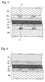
- Fig. 4 illustrates a preferable structure of a photoelectric conversion device of the present invention, where a photosensitive layer 20 is applied on a substrate 50 having an electrically conductive layer 10 thereon through an undercoating layer 60, a charge transfer layer 30 and a transparent counter electrically conductive layer 40a are formed thereon, and further a transparent substrate 50a locally having a metal lead 11 thereon is placed so that the metal lead 11 side orients inward.
- This structure allows incidence of light from the counter electrode side.
- Fig. 5 illustrates a preferable structure of a photoelectric conversion device of the present invention, where on two transparent substrates 50 each having a metal lead 11 partially are formed a transparent electrically conductive layer 10a or a transparent counter electrically conductive layer 40a, respectively, and an undercoating layer 60, a photosensitive layer 20 and a charge transfer layer 30 placed between the conductive layers.
- This structure allows incidence of light from both faces of the photoelectric conversion device.
- Fig. 6 illustrates a preferable structure of a photoelectric conversion device of the present invention, where on a transparent substrate 50a having a transparent electrically conductive layer 10a thereon is formed a photosensitive layer 20 through an undercoating layer 60, a charge transfer layer 30 and a counter electrically conductive layer 40 are applied thereon, and further a substrate 50 is placed thereon.
- This structure allows incidence of light from the electrically conductive layer side.
- Fig. 7 illustrates a preferable structure of a photoelectric conversion device of the present invention, where on a substrate 50 having an electrically conductive layer 10 thereon is applied a photosensitive layer 20 through an undercoating layer 60, a charge transfer layer 30 and a transparent counter electrically conductive layer 40a are applied thereon, and further a transparent substrate 50a is placed thereon.
- This structure allows incidence of light from the counter electrode side.
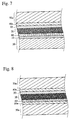
- Fig. 8 illustrates a preferable structure of a photoelectric conversion device of the present invention, where on a transparent substrate 50a having a transparent electrically conductive layer 10a thereon is applied a photosensitive layer 20 through an undercoating layer 60, a charge transfer layer 30 and a transparent counter electrically conductive layer 40a are applied thereon, and further a transparent substrate 50a is placed thereon.
- This structure allows incidence of light from both faces of the photoelectric conversion device.
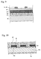
- Fig. 9 illustrates a preferable structure of a photoelectric conversion device of the present invention, where on a substrate 50 having an electrically conductive layer 10 thereon is applied a photosensitive layer 20 through an undercoating layer, a solid charge transfer layer 30 is applied thereon, and further a counter electrically conductive layer 40 or a metal lead 11 is locally applied thereon. This structure allows incidence of light from the counter electrode side.
- the photoelectric cell of the present invention comprises the above-described photoelectric conversion device that is designed to work in the outer circuit.
- the photoelectric cell having the charge transfer layer comprising ionic conductive electrolyte is characterized as a kind of so-called photo-electrochemical cell.
- the side face of the photoelectric cell is preferably sealed with a polymer or an adhesive agent, etc. to prevent deterioration of the compositions thereof and volatility of the content in the cell.
- the outer circuit is connected to the conductive support and the counter electrode via a lead.
- Various known circuits may be used in the present invention.
- the interior structure of the photoelectric conversion device may be essentially the same as above.
- Module structures of the solar cell comprising the photoelectric conversion device of the present invention will be explained below.
- the dye-sensitized solar cell of the present invention may have essentially the same module structure as that of prior art solar cells.
- the solar cell module generally has a structure where a cell is formed on a substrate made of metal, ceramic, etc., they are covered with a packing resin, a protective glass, etc., and light is introduced from an opposite side of the substrate.
- the solar cell module may have a structure where a cell is formed on a substrate made of a transparent material such as a tempered glass, and light is introduced from the transparent substrate side.
- a module structure are structures that are called "superstraight type", "substrate type” or "potting type", substrate-integrated type structure used for an amorphous silicon solar cell, etc.
- the dye-sensitized solar cell of the present invention may have a module structure properly selected from the above structures in accordance with ends, places and environment at use.
- the super straight type modules and the substrate type modules generally have a structure where cells are set at a regular intervals between substrates, adjoining cells are connected by a metal lead, a flexible wirering, etc., and collector electrodes are set at the outer marginal portion so that a generated electric power can be delivered to the outside.
- One or both side of the substrates is transparent and subjected to a reflection-preventing treatment.
- Various kinds of plastic material such as ethylene vinyl acetate (EVA) may be contained between the substrate and the cell to protect the cell or to improve a collector efficiency.
- EVA ethylene vinyl acetate
- Such a plastic material is may be used in a form of a film or a packing resin.
- the substrate of one side can be omitted by forming a surface protective layer composed of a transparent plastic film, or by hardening the above-described packing resin to give a protection function.
- the periphery of the substrates may be sandwiched and fixed by metallic flames, and the substrates and the flames may be sealed with a sealant.
- flexible materials may be used for the cell proper, the substrate, the packing agent and the sealant to constructing the solar cell on a curved surface.
- the super straight type solar cell module may be manufactured by the following steps of: placing cells on a front substrate sent out from a substrate-supplying device together with lead lines for connecting a sealant to the cells and a sealant for back surface while carrying the front substrate by a belt conveyer, etc.; placing a back substrate or a back cover thereon; and setting flames at the outer edge portion.
- the substrate type solar cell may be manufactured by the following steps of: placing cells on a substrate sent out from a substrate-supplying device together with lead lines for connecting the cells and a sealant, etc. while carrying the substrate by a belt conveyer, etc.; placing a front cover thereon; and setting flames at the outer edge portion.
- Fig. 10 shows structure of an embodiment of the substrate-integrated type solar cell produced by modularizing a photoelectric conversion device of the present invention.
- the solar cell shown in Fig. 10 has a structure where cells having a transparent electrically conductive layer 10a, a photosensitive layer 20 containing dye-adsorbed TiO 2 , a solid charge transfer layer 30 and a metal counter electrically conductive layer 40 are modularized on one surface of a transparent substrate 50a, and a reflection-preventing layer 70 is applied on the other surface of the substrate.
- a desired module structure can be obtained by patterning according to a semiconductor process technique such as selective metal plating, selective etching, CVD, PVD, etc., or a mechanical method such as laser scribing, plasma CVM, polishing, etc. so that the transparent electrically conductive layers, the photosensitive layers, the charge transfer layers and the counter electrode etc. are three-dimensionally arranged at a regular interval on the substrate.
- a semiconductor process technique such as selective metal plating, selective etching, CVD, PVD, etc.
- a mechanical method such as laser scribing, plasma CVM, polishing, etc.
- various materials such as a liquid EVA (ethylene vinyl acetate), an EVA film, a mixture of fluorinated vinylidene copolymer and an acrylic resin, etc. may be used in accordance with objects such as application of weather-resistance or electric insulation, improvement in light-condensing efficiency, protection of a cell (improvement in impact resistance), etc.
- the outer edge of the module and the frame surrounding the fringe are preferably sealed with the sealant having high weather-resistance and moisture permeability.
- the strength and light transmittance of the sealed cell can be enhanced by adding a transparent filter into the sealant.
- a method suited to a property of the sealant is preferably used.
- Various methods therefor may be used such as roll pressurization followed by thermal adherence, vacuum pressurization followed by thermal adherence, etc. for the film sealant, and roll coat, bar coat, spray coat, screen printing, etc. for the liquid or paste sealant.
- a flexible material such as PET and PEN is used for a substrate, because after constructing the cells on a roll-like support, the sealing layer can be successively laminated according to the above-described methods to obtain a high productivity.
- the light-taking surface of the substrate, generally a tempered glass substrate, of the module may be subjected to a reflection-preventing treatment.
- the reflection-preventing treatment may comprise laminating a reflection-preventing film, coating a reflection-preventing layer, etc.
- the surface of the solar cell may be grooved or textured, thereby enhancing efficiency of utilizing incident light.
- the light reflectance may be increased by vapor-depositing or metal-plating the substrate with Ag, Al, etc. after a mirror plane-polishing, applying a layer comprising an Al-Mg alloy, an Al-Ti alloy, etc. as reflective layer at the lowest layer in the solar cell, making the lowest layer to a texture structure by annealing.
- the cells are generally connected each other by a wire bonding method or using an electrically conductive flexible sheet.
- the cells may be connected by methods such as electrically connecting while fixing the cells by an electrically conductive adhesives, adhesive tapes, etc., and pattern-coating an electrically conductive hot melt at an intended position.
- a solar cell comprising a flexible support made of a polymer film, etc. may be manufactured by a method comprising the steps: forming cells in the same manner as described above while sending out a roll-like support; cutting it to an intended size; and sealing the marginal portion thereof with a flexible, moisture permeable material.
- the solar cell may have a module structure called "SCAF" described in Solar Energy Materials and Solar Cells, 48, p 383 to 391. Further, the solar cell comprising the flexible support may be used while adhered and fixed to a curved glass, etc.
- the solar cells comprising the photoelectric conversion device of the present invention may have various kinds of forms and functions in accordance with ends of use and environment of use.
- the resultant mixture was washed with water, and purified by column chromatography using Sephadex column LH-20 (developing solvent: methanol) to obtain 0.18 g of the metal complex dye D-1 (black crystal, 92 % yield).
- the structure of the product was identified by MS spectra and elemental analysis.
- the metal complex dye D-2 and D-8 were synthesized in the same manner as syntheses of D-1 and D-7 except that potassium oxalate 4 was used in place of sodium hydroxamate 3 in the same molar amount and that NH 4 PF 6 was not added to the reaction mixture.
- the structures of the products were identified by MS spectra and elemental analysis.
- the metal complex dye D-3 and D-9 were synthesized in the same manner as syntheses of D-1 and D-7 except for using sodium dithiocarbamate 5 in place of sodium hydroxamate 3 in the same molar amount.
- the structures of the products were identified by MS spectra and elemental analysis.
- the metal complex dye D-35 and D-39 were synthesized in the same manner as syntheses of D-2 and D-8 except for using BL-11 synthesized by a method described in J. Am. Chem. Soc., 109, 2691 (1987) in place of dipyridyl pyrazine BL-1 in the same molar amount.
- the structures of the products were identified by MS spectra and elemental analysis.
- the metal complex dyes represented by the general formula (I) according to the present invention can be also easily synthesized by using suitable ligands in a similar method to above.
- Compounds used for the ligands are commercially available, or can be easily synthesized referring to Inorg. Chim. Acta., 206, 69 (1993), Inorg. Chem., 29, 1888 (1990), J. Am. Chem. Soc., 109, 2691 (1987), Inorg. Chem., 29, 4750 (1990), Inorg. Chem., 28, 1520 (1989), Inorg. Chem., 29, 167 (1990), Inorg. Chem., 28, 2465 (1989), Chem. Eur.
- the metal complex dye used in the present invention had a maximum absorption wavelength longer than those of the comparative dyes 1 and 2. Accordingly, the photoelectric cell utilizing the metal complex dye of the present invention can efficiently convert in longer wavelength light into electricity as compared with a prior art.
- a stainless steel vessel coated with Teflon inside and having an inner volume of 200 ml was charged with 15 g of titanium dioxide Degussa P-25 manufactured by Nippon Aerosil K.K., 45 g of water, 1 g of dispersant Triton X-100 manufactured by Aldrich, and 30 g of zirconia beads having a diameter of 0.5 mm manufactured by Nikkato K.K. These contents were subjected to a dispersion treatment at 1500 rpm for 2 hours by means of a sand-grinder mill manufactured by Imex K.K. The zirconia beads were removed by filtration to obtain the titanium dioxide dispersion. The average particle diameter of the titanium dioxide particles in the dispersion was 2.5 ⁇ m. The particle diameter was measured by Master Sizer manufactured by MALVERN.
- the above-described dispersion was coated on an electrically conductive surface of a conductive glass having a fluorine-doped tin oxide layer thereon by a doctor blade.
- This conductive glass manufactured by Nippon Sheet Glass Co., Ltd. had a surface resistance of approximately 10 ⁇ /square.
- a coating thickness of the dispersion was 140 ⁇ m in wet state, and a coating amount of the semiconductor particles was 15 g/m 2 .
- the coated glasses were air-dried for 30 minutes at 25 °C. Then, the glasses were placed in an electric furnace (muffle furnace FP-32, manufactured by Yamato Science K.K.), followed by calcinating at 450 °C for 30 minutes to obtain TiO 2 electrodes.
- the electrodes were taken out of the furnace and cooled, they were immersed in the methanol solution comprising the metal complex dye shown in Table 2 for 3 hours to adsorbing the dye, respectively.
- the concentration of the dye in the methanol solution was 3 ⁇ 10 -4 mol/l.
- the dye-adsorbed TiO 2 electrodes were further immersed in 4-t-butylpyridine for 15 minutes, then washed with methanol and air-dried.
- the thickness of thus-obtained photosensitive layer was 10 ⁇ m, and an adsorbed amount of the metal complex dye was 0.1 to 10 mmol/m 2 .
- the 20 mm ⁇ 20 mm of dye-sensitized TiO 2 electrode glass substrate prepared as described above was put on platinum-vapor deposited glass having the same size as the TiO 2 electrode through a spacer.
- an electrolysis solution comprising N-methyl-2-oxazolydinone, and 0.65 mol/l of 1-butyl-3-methylimidazolium iodide and 0.05 mol/l of iodine as an electrolyte was permeated into a crevice between the glasses through capillarity to be introduced into the TiO 2 electrode, thereby obtaining a photoelectric cell.
- the photoelectric cell as shown in Fig.
- a stainless steel vessel coated with Teflon inside and having an inner volume of 200 ml was charged with 15 g of titanium dioxide Degussa P-25 manufactured by Nippon Aerosil K.K., 45 g of water, 1 g of dispersant Triton X-100 manufactured by Aldrich, and 30 g of zirconia beads having a diameter of 0.5 mm manufactured by Nikkato K.K. These contents were subjected to a dispersion treatment at 1500 rpm for 2 hours by means of a sand-grinder mill manufactured by Imex K.K. The zirconia beads were removed by filtration to obtain the titanium dioxide dispersion. The average particle diameter of the titanium dioxide particles in the dispersion was 2.5 ⁇ m. Incidentally, the particle diameter was measured by Master Sizer manufactured by MALVERN.
- the above-described dispersion was coated on an electrically conductive surface of a conductive glass having a fluorine-doped tin oxide layer thereon by a glass bar.
- a conductive glass Used as the conductive glass was 20 mm ⁇ 20 mm of TCO Glass-U manufactured by Asahi Glass K.K. with surface resistance of approximately 30 ⁇ /square.
- a coating amount of the semiconductor particles was 20 g/m 2 .
- the dispersion at once after adhesive tape was attached to a part of the conductive surface (3 mm from the edge) of each conductive glass as a spacer, and the glasses were arranged so that the adhesive tapes come to both edges thereof.
- the coated glasses were air-dried for one day at a room temperature after peeling the adhesive tapes.
- the glasses were placed in an electric furnace (muffle furnace FP-32, manufactured by Yamato Science K.K.), followed by calcinating at 450 °C for 30 minutes to obtain TiO 2 electrodes.
- the electrodes were taken out of the furnace and cooled, they were immersed in the methanol solutions comprising the metal complex dye shown in Table 3 for 15 hours to adsorbing the dyes, respectively.
- the concentration of the dye in the methanol solution was 3 ⁇ 10 -4 mol/l.
- the dye-adsorbed TiO 2 electrodes were further immersed in 4-t-butylpyridine for 15 minutes, then washed with ethanol and air-dried.
- the thickness of thus-obtained photosensitive layer was 10 ⁇ m.
- the 20 mm ⁇ 20 mm of dye-sensitized TiO 2 electrode glass substrate prepared as described above was put on platinum-vapor deposited glass having the same size as the TiO 2 electrode. Then, an electrolysis solution comprising 3-methoxypropionitrile, and 0.65 mol/l of 1-methyl-3-hexylimidazolium iodide and 0.05 mol/l of iodine as an electrolyte was permeated into a crevice between the glasses through capillarity to be introduced into the TiO 2 electrode, thereby obtaining a photoelectric cell. According to this example, the photoelectric cell as shown in Fig.
- the photoelectric cell using the dyes could not convert the light into electricity.
- the photoelectric cells utilizing the dyes represented by the general formula (I) of the present invention exhibited an excellent photoelectric conversion efficiency to such a long wavelength light.
- the metal complex dye represented by the general formula (I) according to the present invention has a high absorbability against light in a large wavelength region containing visible region to infrared region. Consequently, the photoelectric conversion device utilizing the dye exhibits a high photoelectric conversion efficiency to a light in the visible region to the infrared region.
- the photoelectric cell comprising the device of the present invention is extremely useful as a solar cell.
Abstract
Description
- The present invention relates to a metal complex dye, a photoelectric conversion device comprising semiconductor particles sensitized by the metal complex dye, and a photoelectric cell comprising the photoelectric conversion device.
- Solar cells for the solar power generation comprising a monocrystalline silicon, a polycrystalline silicon, an amorphous silicon, cadmium telluride, indium copper selenide, etc. have been the subject of practical use and a major object of research and development. However, for a widespread use of the solar cell as a home power source, etc., there are such problems as a high production cost, difficulty in security of raw materials, and a long energy payback time, therefore, these obstacles must be overcome. On the other hand, a variety of solar cells comprising organic materials are proposed with the objects of increasing the surface area of the cell, lowering the price thereof, etc. However, they generally have such defects as a low conversion efficiency and a poor durability.
- Under these circumstances, Nature, vol. 353, pp. 737 to 740 (1991), United States Patent No. 4,927,721 and WO 94/04497 proposed a wet-type photoelectric conversion device and a solar cell each comprising a titanium dioxide porous thin film spectrally sensitized with a ruthenium complex dye as a working electrode, and materials and a production technique for making the same. The primary advantage for the wet-type device is that a low-priced photoelectric conversion device can be provided because an inexpensive oxide semiconductor such as titanium dioxide can be used without purification thereof to a high purity. The secondary advantage therefor is that a light in almost whole visible wavelength region can be convened to electricity because the dye used therein exhibits a broad absorption spectrum.
- However, known ruthenium complex dyes are disadvantageous in hardly absorbing an infrared ray with a wavelength of 700 nm or more. Consequently, a photoelectric conversion device comprising such a dye exhibits a low photoelectric conversion efficiency at infrared region. It has been desired to develop a dye having a high absorbancy at a large wave range containing visible region to infrared region.
- An object of the present invention is to provide a metal complex dye having a high absorbability not only at visible region but also at infrared region, which is able to efficiently sensitize semiconductor particles, a photoelectric conversion device comprising the metal complex dye which exhibits an excellent photoelectric conversion efficiency, and a photoelectric cell comprising the photoelectric conversion device.
- As a result of intense research in view of the above object, the inventor has found that a metal complex dye comprising two or more metal atoms, a ligand having two or more moieties for bidentate or tridentate coordination to the metal atoms, and optional bidentate or tridentate ligand having nitrogen atoms for coordinating to the metal atom and monodentate or bidentate ligand(s) which coordinates to the metal atom via a dithiocarbamate group, a thiocyanate group, etc. has a high absorbancy in not only at visible region but also at long wavelength region and can efficiently sensitize semiconductor particles, and that a photoelectric conversion device comprising the metal complex dye exhibits an excellent photoelectric conversion efficiency, so that it is useful for a photoelectric cell. The present invention has been accomplished by the findings.
- Thus, the present invention provides the photoelectric conversion device comprising semiconductor particles sensitized by the metal complex dye represented by the following general formula (I):
- BL represents a ligand having two or more moieties for bidentate or tridentate coordination to the metal atoms;
- LL1 and LL2 independently represent a bidentate or tridentate ligand
represented by the following general formula (II):
wherein Za, Zb and Zc independently represent nonmetallic atoms forming a 5- or 6-membered ring, a being 0 or 1;

- X1 and X2 independently represent a monodentate or bidentate ligand which coordinates to said metal atom via one or two groups selected from the group consisting of an acyloxy group, an acylthio group, a thioacyloxy group, a thioacylthio group, an acylaminooxy group, a thiocarbamate group, a dithiocarbamate group, a thiocarbonate group, a dithiocarbonate group, a trithiocarbonate group, an acyl group, a thiocyanate group, an isothiocyanate group, a cyanate group, an isocyanate group, a cyano group, an alkylthio group, an arylthio group, an alkoxy group and an aryloxy group, or a monodentate or bidentate ligand selected from the group consisting of halogen atoms, carbonyl, dialkylketones, 1,3-diketones, carbonamides, thiocarbonamides and thioureas;
- m1 and m3 independently represent 0 or 1;
- m2 represents an integer of 0 to 4, and X1's may be the same or different ligands that may be bonded together when m2 is 2 or more;
- m4 represents an integer of 0 to 4, and X2's may be the same or different ligands that may be bonded together when m4 is 2 or more; and
- CI represents a counter ion optionally contained to neutralize charge of said metal complex dye.
-
- The photoelectric cell of the present invention is characterized by the use of the photoelectric conversion device.
- With respect to the metal complex dye, the photoelectric conversion device and the photoelectric cell of the present invention, the absorbancy at the long wavelength region and the photoelectric conversion efficiency are further improved by satisfying at least one of the following conditions (1) to (23).
- (1) M1 and M2 are preferably a metal atom that is able to form four- or six-coordinated complex, more preferably Ru, Fe, Os, Cu, W, Cr, Mo, Ni, Pd, Pt, Co, Ir, Rh, Mn or Zn, particularly preferably Ru, Fe, Os or Cu, most preferably Ru, respectively.
- (2) It is preferable that BL is represented by any one of the following
general formulae (III-1) to (III-3):
wherein Zd to Zk independently represent nonmetallic atoms forming a 5-or 6-membered ring, b being 0 or 1.

- (3) It is preferable that Ze and Zh in the general formulae (III-1) and (III-2) form a pyrazine ring.
- (4) It is more preferable that BL is represented by any one of the
following general formulae B-1 to B-10:
wherein R11 to R20 independently represent a substituent that may be bonded to any carbon atom forming a ring, c1 to c6 and c8 independently represent an integer of 0 to 8, c7 and c9 independently represent an integer of 0 to 6, and c10 represents an integer of 0 to 4.

- (5) It is furthermore preferable that BL is represented by any one of the general formulae B-1 to B-4.
- (6) It is preferable that R11 to R20 in the general formulae B-1 to B-10 independently represent an alkyl group, an alkenyl group, an aryl group, a hydroxyl group, an alkoxy group, an amino group, an alkoxycarbonyl group, a carboxyl group, a sulfonic acid group, a phosphoryl group, a phosphonyl group or a halogen atom.
- (7) It is preferable that BL is represented by the following general
formula B-11:
wherein L1 represents a single bond, an oxygen atom, a sulfur atom, an alkenylene group, an alkynylene group, an arylene group or a divalent heterocyclic group, R21 represents a carboxyl group, a sulfonic acid group, a hydroxyl group, a hydroxamic acid group, a phosphoryl group or a phosphonyl group, R22 represents a substituent, R21 and R22 may be bonded to any carbon atom of a bipyridine ring, d1 and d2 independently represent an integer of 0 to 4, R21's may be the same or different groups when d1 is 2 or more, R22's may be the same or different groups that may be bonded together to form a ring when d2 is 2 or more, and e represents an integer of 0 to 2.

- (8) It is preferable that BL is represented by any one of the following
general formulae B-12 to B-15:
wherein R23 to R26 independently represent a carboxyl group, a sulfonic acid group, a hydroxyl group, a hydroxamic acid group, a phosphoryl group or a phosphonyl group, R27 to R30 independently represent a substituent, R23 to R30 may be bonded to any carbon atom forming an aromatic ring, f1 to f4 independently represent an integer of 0 to 4, f5 to f8 independently represent an integer of 0 to 10, R23's to R26's may be the same or different groups when f1 to f4 are 2 or more, R27's to R30's may be the same or different groups that may be bonded together to form a ring when f5 to f8 are 2 or more, and L2 represents a divalent linking group.

- (9) It is more preferable that BL is represented by the general formula B-13 or B-14, and L2 represents an oxygen atom, a sulfur atom, an alkenylene group, an alkynylene group, an arylene group or a divalent heterocyclic group.
- (10) It is preferable that R23 to R26 in the general formulae B-12 to B-15 are independently a carboxyl group or a phosphonyl group.
- (11) It is preferable that R27 to R30 in the general formulae B-12 to B-15 independently represent an alkyl group, an alkenyl group, a cycloalkyl group, an aryl group, a heterocyclic group, an alkoxy group, an aryloxy group, an acyloxy group, an alkoxycarbonyl group, a carbamoyl group, an acylamino group, an amino group, an acyl group, a sulfonamido group, a cyano group, a hydroxyl group or a halogen atom.
- (12) It is preferable that f1 to f4 in the general formula B-12 to B-15 independently represent an integer of 1 to 4
- (13) Rings formed by Za, Zb and Zc in the general formula (II) are preferably a pyridine ring, a pyrimidine ring, a pyrazine ring, a pyridazine ring, a pyrazole ring, an imidazole ring, a triazole ring, a thiazole ring, an oxazole ring, a benzimidazole ring, a benzotriazole ring, a benzoxazole ring or a benzothiazole ring, particularly preferably a pyridine ring or an imidazole ring, respectively.
- (14) It is preferable that LL1 and LL2 independently represent a bidentate
or tridentate ligand represented by any one of the following general
formulae (IV-1) to (IV-8):
wherein R31 to R38 independently represent a carboxyl group, a sulfonic acid group, a hydroxyl group, a hydroxamic acid group, a phosphoryl group or a phosphonyl group, R39 to R46 independently represent a substituent, R47 to R51 independently represent a hydrogen atom, an alkyl group, an alkenyl group or an aryl group, R31 to R46 may be bonded to any carbon atom forming a ring, g1 to g8, g13, g14 and g16 independently represent an integer of 0 to 4, g9 to g12 and g15 independently represent an integer of 0 to 6, R31's to R38's may be the same or different groups when g1 to g8 are 2 or more, and R39's to R46's may be the same or different groups that may be bonded together to form a ring when g9 to g16 are 2 or more. LL1 and LL2 are more preferably represented by any one of the general formulae (IV-1) to (IV-6), respectively.

- (15) It is preferable that R31 to R38 in the general formulae (IV-1) to (IV-8) independently represent a carboxyl group or a phosphonyl group.
- (16) It is preferable that R39 to R46 in the general formulae (IV-1) to (IV-8) independently represent an alkyl group, an alkenyl group, a cycloalkyl group, an aryl group, a heterocyclic group, an alkoxy group, an aryloxy group, an acyloxy group, an alkoxycarbonyl group, a carbamoyl group, an acylamino group, an amino group, an acyl group, a sulfonamido group, a cyano group, a hydroxyl group or a halogen atom.
- (17) It is preferable that m1 and m3 are 0.
- (18) It is preferable that m1 and m3 are 0, and m2 and m4 are 2.
- (19) It is preferable that m1 and m3 are 0, and m2 and m4 are 3.
- (20) It is preferable that m1 and m3 are 1, and m2 and m4 are 1.
- (21) It is preferable that the metal complex dye comprises at least one acidic group.
- (22) It is more preferable that the metal complex dye comprises at least one group selected from the group consisting of a carboxyl group, a sulfonic acid group, a hydroxyl group, a hydroxamic acid group, a phosphoryl group and a phsphonyl group.
- (23) It is preferable that the semiconductor particles are titanium oxide particles.
-
- As for the metal complex dye according to a particularly preferable embodiment of the present invention, in the general formula (I), M1 and M2 independently represent a metal atom that is able to form four- or six-coordinated complex; BL represents a ligand having two or more moieties for bidentate coordination to the metal atoms, represented by any one of the general formulae B-1 to B-10; LL1 and LL2 independently represent a bidentate ligand represented by the general formulae (IV-1) or (IV-6); X1 and X2 independently represent a monodentate or bidentate ligand which coordinates to said metal atom via one or two groups selected from the group consisting of an acyloxy group, an acylthio group, a thioacyloxy group, a thioacylthio group, an acylaminooxy group, a thiocarbamate group, a dithiocarbamate group, a thiocarbonate group, a dithiocarbonate group, a trithiocarbonate group, an acyl group, a thiocyanate group, an isothiocyanate group, a cyanate group, an isocyanate group, a cyano group, an alkylthio group, an arylthio group, an alkoxy group and an aryloxy group, or a monodentate or bidentate ligand selected from the group consisting of halogen atoms, carbonyl, dialkylketones, 1,3-diketones, carbonamides, thiocarbonamides and thioureas; m1 and m3 independently represent 0 or 1; m2 represents an integer of 1 to 4, and X1's may be the same or different ligands that may be bonded together when m2 is 2 or more; m4 represents an integer of 1 to 4, and X2's may be the same or different ligands that may be bonded together when m4 is 2 or more; and CI represents a counter ion optionally contained to neutralize charge of said metal complex dye.
- In this embodiment, it is preferable that M1 and M2 are Ru, BL is represented by any one of the general formulae B-1 to B-4, and X1 and X2 independently represent a monodentate or bidentate ligand which coordinates to Ru via one or two groups selected from the group consisting of an acyloxy group, an acylaminooxy group, a dithiocarbamate group, a thiocyanate group, an isothiocyanate group, a cyanate group, an isocyanate group, an alkylthio group and an arylthio group.
- As for the metal complex dye according to another particularly preferable embodiment of the present invention, in the general formula (I), M1 and M2 are Ru; BL represents a ligand having two or more moieties for tridentate coordination to Ru, represented by any one of the general formulae B-12 to B-15; LL1 and LL2 independently represent a bidentate or tridentate ligand represented by any one of the general formulae (IV-1) to (IV-8); X1 and X2 independently represent a monodentate or bidentate ligand which coordinates to Ru via one or two groups selected from the group consisting of an acyloxy group, an acylthio group, a thioacyloxy group, a thioacylthio group, an acylaminooxy group, a thiocarbamate group, a dithiocarbamate group, a thiocarbonate group, a dithiocarbonate group, a trithiocarbonate group, an acyl group, a thiocyanate group, an isothiocyanate group, a cyanate group, an isocyanate group, a cyano group, an alkylthio group, an arylthio group, an alkoxy group and an aryloxy group, or a monodentate or bidentate ligand selected from the group consisting of halogen atoms, carbonyl, dialkylketones, 1,3-diketones, carbonamides, thiocarbonamides and thioureas; m1 and m3 independently represent 0 or 1; m2 represents an integer of 0 to 3, and X1's may be the same or different ligands that may be bonded together when m2 is 2 or more; m4 represents an integer of 0 to 3, and X2's may be the same or different ligands that may be bonded together when m4 is 2 or more; and CI represents a counter ion optionally contained to neutralize charge of said metal complex dye.
-
- Fig. 1 is a partial cross sectional view showing a preferable structure of a photoelectric conversion device of the present invention,
- Fig. 2 is a partial cross sectional view showing a preferable structure of a photoelectric conversion device of the present invention,
- Fig. 3 is a partial cross sectional view showing a preferable structure of a photoelectric conversion device of the present invention,
- Fig. 4 is a partial cross sectional view showing a preferable structure of a photoelectric conversion device of the present invention,
- Fig. 5 is a partial cross sectional view showing a preferable structure of a photoelectric conversion device of the present invention,
- Fig. 6 is a partial cross sectional view showing a preferable structure of a photoelectric conversion device of the present invention,
- Fig. 7 is a partial cross sectional view showing a preferable structure of a photoelectric conversion device of the present invention,
- Fig. 8 is a partial cross sectional view showing a preferable structure of a photoelectric conversion device of the present invention,
- Fig. 9 is a partial cross sectional view showing a preferable structure of a photoelectric conversion device of the present invention, and
- Fig. 10 is a partial cross sectional view showing an example of a structure of a substrate-integrated type solar cell module comprising a metal complex dye of the present invention.
-
- A metal complex dye for use in a photoelectric conversion device of the present invention is represented by the following general formula (I).
- M1 and M2 independently represent a metal atom. M1 and M2 may be the same or different atoms. M1 and M2 are preferably a metal atom that is able to form four- or six-coordinated complex, more preferably Ru, Fe, Os, Cu, W, Cr, Mo, Ni, Pd, Pt, Co, Ir, Rh, Mn or Zn, particularly preferably Ru, Fe, Os or Cu, most preferably Ru, respectively.
- In the general formula (I), BL represents a ligand having two or more moieties for bidentate or tridentate coordination to the metal atoms. BL preferably has two moieties for bidentate or tridentate coordination. When BL has three or more moieties for coordination, the metal complex dye represented by the general formula (I) may comprises metal atom(s) other than M1 and M2, and ligand(s) coordinating thereto. BL preferably coordinates to the metal atoms via atoms selected from the group consisting of a nitrogen atom, a carbon atom, an oxygen atom and a sulfur atom. Among them, a nitrogen atom and carbon atom are more preferred, and a nitrogen atom is particularly preferred.
- It is preferable that BL is represented by any one of the following general formulae (III-1) to (III-3).

- In the general formulae (III-1) to (III-3), Zd to Zk independently represent nonmetallic atoms forming a 5- or 6-membered ring, preferably composed of carbon, hydrogen, nitrogen, oxygen, sulfur, phosphorus and/or halogen atoms. They preferably form an aromatic ring, respectively. The 5- or 6-membered ring may be substituted or unsubstituted ring that may be a monocyclic or a condensed ring. These rings formed by Zd to Zk may be bonded together to form a condensed ring.
- As for the aromatic rings formed by Zd, Zf, Zg, Zi, Zj and Zk, such rings as a pyrazole ring, an imidazole ring, an oxazole ring, a thiazole ring, a triazole ring, a benzimidazole ring, a benzotriazole ring, a benzoxazole ring and a benzothiazole ring are preferred as a 5-membered ring, and such rings as a pyridine ring, a pyrimidine ring, a pyridazine ring and a pyrazine ring are preferred as a 6-membered ring. Of these rings, more preferred are an imidazole ring and a pyridine ring, and particularly preferred is a pyridine ring.
- The rings independently formed by Ze and Zh in the general formulae (III-1) and (III-2) are preferably a pyrazine ring, a pyridazine ring or a tetradine ring, more preferably a pyrazine ring.
- b in the general formula (III-3) is 0 or 1, preferably 0.
- It is more preferable that BL is represented by any one of the following general formulae B-1 to B-10. BL is furthermore preferably represented by any one of the general formulae B-1 to B-4, B-7 and B-10, particularly preferably represented by any one of the general formulae B-1 to B-4 and B-10, most preferably represented by any one of the general formulae B-1 to B-4.

- In the general formulae B-1 to B-10, R11 to R20 independently represent a substituent that may be bonded to any carbon atom forming a ring. It is preferable that R11 to R20 independently represent an alkyl group, an alkenyl group, an aryl group, a hydroxyl group, an alkoxy group, an amino group, an alkoxycarbonyl group, a carboxyl group, a sulfonic acid group, a phosphoryl group, a phosphonyl group or a halogen atom. Among them, more preferred are an alkyl group, an alkenyl group, a hydroxyl group, an alkoxy group, a carboxyl group, a sulfonic acid group, a phosphoryl group and a phosphonyl group.
- In the general formulae B-1 to B-10, c1 to c6 and c8 independently represent an integer of 0 to 8, c7 and c9 independently represent an integer of 0 to 6, and c10 represents an integer of 0 to 4. c1 to c10 are preferably represent an integer of 0 to 2, respectively.
- In addition, also given as preferred BL is a ligand represented by the following general formula B-11.

- In the general formula B-11, L1 represents a single bond, an oxygen atom, a sulfur atom, an alkenylene group preferably having 2 to 20 carbon atoms such as an ethenylene group, a butadienylene group, etc., an alkynylene group preferably having 2 to 20 carbon atoms such as an ethynylene group, a butadiynylene group, etc., an arylene group preferably having 6 to 26 carbon atoms such as a 1,4-phenylene group, a 1,2-phenylene group, a 1,3-phenylene group, a 1,4-naphtylene group, a 2,5-dimethoxy-1,4-phenylene group, a 4,4-biphenylene group, etc. or a divalent heterocyclic group preferably having 1 to 26 carbon atoms such as a 2,5-pyridilene group, a 2,5-thienylene group, a 2,5-furanylene group, a 2,5-pyrrolylene group, a 2,5-benzothienylene group, etc. L1 is more preferably a single bond, an alkenylene group, an alkynylene group or a divalent heterocyclic group, particularly preferably an ethenylene group, an ethynylene group, a butadiynylene group or a 2,5-thienylene group.

- In the general formula B-11, R21 independently represents a carboxyl group, a sulfonic acid group, a hydroxyl group, a hydroxamic acid group preferably having 1 to 20 carbon atoms such as -CONHOH, - CONCH3OH, etc., a phosphoryl group such as -OP(O)(OH)2, etc. or a phosphonyl group such as -P(O)(OH)2. Of these groups, preferred are a carboxyl group, a phosphonyl group and a phosphoryl group, more preferred are a carboxyl group and a phosphonyl group, and the most preferred is a carboxyl group.
- In the general formula B-11, R22 represents a substituent. Preferred examples thereof include an alkyl group preferably having 1 to 20 carbon atoms such as a methyl group, an ethyl group, an isopropyl group, a t-butyl group, a pentyl group, a heptyl group, a 1-ethylpentyl group, a benzyl group, a 2-ethoxyethyl group, a 1-carboxymethyl group, etc., an alkenyl group preferably having 2 to 20 carbon atoms such as a vinyl group, an allyl group, an oleyl group, etc., an alkynyl group preferably having 2 to 20 carbon atoms such as an ethynyl group, a butadiynyl group, a phenylethynyl group, etc., a cycloalkyl group preferably having 3 to 20 carbon atoms such as a cyclopropyl group, a cyclopentyl group, a cyclohexyl group, a 4-methylcyclohexyl group, etc., an aryl group preferably having 6 to 26 carbon atoms such as a phenyl group, a 1-naphthyl group, a 4-methoxyphenyl group, a 2-chlorophenyl group, a 3-methylphenyl group, etc., a heterocyclic group preferably having 2 to 20 carbon atoms such as a 4-pyridyl group, a 1-imidazolyl group, a 2-benzoimidazolyl group, a 2-thiazolyl group, a 2-oxazolyl group, etc., an alkoxy group preferably having 1 to 20 carbon atoms such as a methoxy group, an ethoxy group, an isopropyloxy group, a benzyloxy group, etc., an aryloxy group preferably having 6 to 26 carbon atoms such as a phenoxy group, a 1-naphthyloxy group, a 3-methylphenoxy group, a 4-methoxyphenoxy group, etc., an alkoxycarbonyl group preferably having 2 to 20 carbon atoms such as an ethoxycarbonyl group, a 2-ethylhexyloxycarbonyl group, etc., an amino group preferably having 0 to 20 carbon atoms such as an amino group, an N,N-dimethylamino group, an N,N-diethylamino group, an N-ethylamino group, an anilino group, etc., an acyl group preferably having 1 to 20 carbon atoms such as an acetyl group, a benzoyl group, etc., a sulfonamido group preferably having 0 to 20 carbon atoms such as an N,N-dimethylsulfonamido group, an N-phenylsulfonamido group, etc., an acyloxy group preferably having 1 to 20 carbon atoms such as an acetyloxy group, a benzoyloxy group, etc., a carbamoyl group preferably having 1 to 20 carbon atoms such as an N,N-dimethylcarbamoyl group, an N-phenylcarbamoyl group, etc., an acylamino group preferably having 1 to 20 carbon atoms such as an acetylamino group, a benzoylamino group, etc., a cyano group, or a halogen atom such as a fluorine atom, a chlorine atom, a bromine atom, an iodine atom, etc.
- Among them, more preferred are an alkyl group, an alkenyl group, an alkynyl group, an alkoxy group, an aryloxy group, an amino group and an acylamino group, furthermore preferred are an alkyl group, an alkenyl group, an alkoxy group, an amino group and an acylamino group, particularly preferred are an alkyl group, an alkoxy group and an amino group.
- In the general formula B-11, d1 indicating the number of R21 represents an integer of 0 to 4. R21's may be the same or different groups when d1 is 2 or more. R21 may be bonded to any carbon atom of a bipyridine ring. d1 is preferably an integer of 0 to 2, more preferably 0 or 1.
- In the general formula B-11, d2 indicating the number of R22 represents an integer of 0 to 4. R22's may be the same or different groups that may be bonded together to form a ring when d2 is 2 or more. The preferable ring formed by R22's is a benzene ring, a pyridine ring, a cyclohexane ring, a cyclopentane ring, etc. R22 may be bonded to any carbon atom of a bipyridine ring. d2 is preferably an integer of 0 to 2, more preferably 0 or 1.
- In the general formula B-11, e is an integer of 0 to 2, preferably 0.
- It is preferable that the ligand BL represented by the general formula B-11 is further represented by the following general formula B-11' or B-11''.In the general formula B-11' or B-11'', L1, R21, R22, d1 and d2 are the same as those in the general formula B-11.

- Further, a ligand represented by any one of the following general formulae B-12 to B-15 is also given as proffered example of BL. It is more preferably that BL is represented by the general formula B-13 or B-14.

- In the general formulae B-12 to B-15, R23 to R26 independently represent a carboxyl group, a sulfonic acid group, a hydroxyl group, a hydroxamic acid group preferably having 1 to 20 carbon atoms such as - CONHOH, -CONCH3OH, etc., a phosphoryl group such as -OP(O)(OH)2, etc. or a phosphonyl group such as -P(O)(OH)2. Of these groups, preferred are a carboxyl group, a phosphonyl group and a phosphoryl group, more preferred are a carboxyl group and a phosphonyl group, and the most preferred is a carboxyl group.
- In the general formulae B-12 to B-15, R27 to R30 independently represent a substituent. It is preferable that R27 to R30 are independently an alkyl group, an alkenyl group, a cycloalkyl group, an aryl group, a heterocyclic group, an alkoxy group, an aryloxy group, an acyloxy group, an alkoxycarbonyl group, a carbamoyl group, an acylamino group, an amino group, an acyl group, a sulfonamido group, a cyano group, a hydroxyl group or a halogen atom. Preferable examples of these groups are equal to those of R22. R27 to R30 are more preferably an alkyl group, an alkenyl group, an aryl group, a heterocyclic group, an alkoxy group, an alkoxycarbonyl group, an amino group or a halogen atom, particularly preferably an alkyl group, an alkenyl group, an alkoxy group, an alkoxycarbonyl group or an amino group, respectively.
- In the general formulae B-12 to B-15, f1 to f4 are independently an integer of 0 to 4, preferably an integer of 1 to 4. f5 to f8 are independently an integer of 0 to 10, preferably an integer of 0 to 4.
- R23 to R30 may be bonded to any carbon atom forming an aromatic ring. R23's to R26's may be the same or different groups when f1 to f4 are 2 or more, and R27's to R30's may be the same or different groups that may be bonded together to form a ring when f5 to f8 are 2 or more.
- L2 in the general formula B-14 is a divalent linking group, preferably an oxygen atom, a sulfur atom, an alkenylene group preferably having 2 to 20 carbon atoms such as an ethenylene group, a 1,4-buta-1,3-dienylene group, etc., an alkynylene group preferably having 2 to 20 carbon atoms such as an ethynylene group, a 1,4-buta-1,3-diynylene group, etc., an arylene group preferably having 6 to 26 carbon atoms such as a 1,4-phenylene group, a 1,3-phenylene group, a 1,4-naphtylene group, a 1,4-biphenylene group, a 2,3-dimethoxy-1,4-phenylene group, etc. or a divalent heterocyclic group preferably having 1 to 20 carbon atoms such as a 2,5-pyridilene group, a 1,3-imidazolylene group, a 2,5-thienylene group, etc., more preferably an oxygen atom, an arylene group, a 2,5-thienylene group, an alkenylene group or an alkynylene group, particularly preferably a 2,5-thienylene group, an ethenylene group, a 1,4-buta-1,3-dienylene group, an ethynylene group or a 1,4-buta-1,3-diynylene group.
- When BL contains an alkyl group, an alkenyl group, etc., they may be a substituted or unsubstituted group having a straight or branched structure. When BL contains an aryl group, a heterocyclic group, etc., they may be a substituted or unsubstituted group having a monocyclic or condensed ring structure.
- Specific examples BL-1 to BL-99 of the ligand BL will be illustrated below without intention of restricting the scope of the present invention defined by the claims attached hereto.


- In the general formula (I), LL1 and LL2 independently represent a bidentate or tridentate ligand represented by the following general formula (II).LL1 and LL2 may be the same or different ligands, are preferably the same ligands. m1 and m3 each indicating the number of LL1 and LL2 are independently 0 or 1.
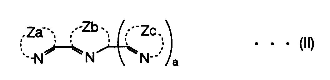
- In the general formula (II), Za, Zb and Zc independently represent nonmetallic atoms forming a 5- or 6-membered ring. The 5- or 6-membered ring may be substituted or unsubstituted ring that may be a monocyclic or a condensed ring. Za, Zb and Zc are preferably composed of carbon, hydrogen, nitrogen, oxygen, sulfur, phosphorus and/or halogen atoms, respectively. They preferably form an aromatic ring. As for the aromatic ring, such rings as an imidazole ring, a triazole ring, a thiazole ring, an oxazole ring, a pyrazole ring, a benzimidazole ring, a benzotriazole ring, a benzoxazole ring and a benzothiazole ring are preferred as a 5-membered ring, and such rings as a pyridine ring, a pyrimidine ring, a pyridazine ring and a pyrazine ring are preferred as a 6-membered ring. Of these rings, more preferred are a benzimidazole ring, an imidazole ring and a pyridine ring, and particularly preferred are an imidazole ring and a pyridine ring, a in the general formula (II) is 0 or 1, preferably 0.
- It is preferable that LL1 and LL2 independently represent a bidentate or tridentate ligand represented by any one of the following general formulae (IV-1) to (IV-8).

- In the general formulae (IV-1) to (IV-8), R31 to R38 independently represent a carboxyl group, a sulfonic acid group, a hydroxyl group, a hydroxamic acid group preferably having 1 to 20 carbon atoms such as - CONHOH, -CONCH3OH, etc., a phosphoryl group such as -OP(O)(OH)2, etc. or a phosphonyl group such as -P(O)(OH)2. Of these groups, preferred are a carboxyl group, a phosphonyl group and a phosphoryl group, more preferred are a carboxyl group and a phosphonyl group, and the most preferred is a carboxyl group.
- In the general formulae (IV-1) to (IV-8), R39 to R46 independently represent a substituent. It is preferable that R39 to R46 are independently an alkyl group, an alkenyl group, a cycloalkyl group, an aryl group, a heterocyclic group, an alkoxy group, an aryloxy group, an acyloxy group, an alkoxycarbonyl group, a carbamoyl group, an acylamino group, an amino group, an acyl group, a sulfonamido group, a cyano group, a hydroxyl group or a halogen atom. Preferable examples of these groups are equal to those of R22. R39 to R46 are more preferably an alkyl group, an alkenyl group, an aryl group, a heterocyclic group, an alkoxy group, an alkoxycarbonyl group, an amino group or a halogen atom, particularly preferably an alkyl group, an alkenyl group, an alkoxy group, an alkoxycarbonyl group or an amino group, respectively.
- When LL1 and LL2 contain an alkyl group, an alkenyl group, etc., they may be a substituted or unsubstituted group having a straight or branched structure. When LL1 and LL2 contain an aryl group, a heterocyclic group, etc., they may be a substituted or unsubstituted group having a monocyclic or condensed ring structure.
- In the general formulae (IV-1) to (IV-8), R47 to R51 independently represent a hydrogen atom, an alkyl group, an alkenyl group or an aryl group. Preferable examples of these groups are equal to those of R22. R47 to R51 are preferably a branched alkyl group or an alkyl group having a carboxyl group, independently.
- In the general formulae (IV-1) to (IV-8), g1 to g8, g13, g14 and g16 independently represent an integer of 0 to 4, and g9 to g12 and g15 independently represent an integer of 0 to 6. g1 to g16 are preferably an integer of 0 to 2, respectively.
- R31 to R46 may be bonded to any carbon atom forming a ring. R31's to R38's may be the same or different groups when g1 to g8 are 2 or more, and R39's to R46's may be the same or different groups that may be bonded together to form a ring when g9 to g16 are 2 or more. It is particularly preferable that R39's, R40's, and R41's are independently an alkyl group or an alkenyl group, and they are bonded together to form a ring when g9, g10 and g11 are 2 or more.
- LL1 and LL2 is more preferably represented by any one of the general formulae (IV-1) to (IV-6), particularly preferably represented by any one of the general formulae (IV-1) to (IV-4) and (IV-6), and the most preferably represented by the general formula (IV-1) or (IV-2).
- Specific examples L-1 to L-89 of the ligand LL1 and LL2 will be illustrated below without intention of restricting the scope of the present invention defined by the claims attached hereto.


- In the general formula (I), X1 and X2 independently represent a monodentate or bidentate ligand. X1 and X2 may be the same or different ligands, are preferably the same ligands. m2 and m4 each indicating the number of X1 and X2 independently represents an integer of 0 to 4. X1's may be the same or different ligands that may be bonded together when m2 is 2 or more, and X2's may be the same or different ligands that may be bonded together when m4 is 2 or more.
- X1 and X2 independently represent a monodentate or bidentate ligand which coordinates to a metal atom via one or two groups selected from the group consisting of an acyloxy group preferably having 1 to 20 carbon atoms such as an acetyloxy group, a benzoyloxy group, a salicyloyloxy group, a glycyloxy group, an N,N-dimethylglycyloxy group, a oxalylene group (-OC(O)C(O)O-), etc., an acylthio group preferably having 1 to 20 carbon atoms such as an acetylthio group, a benzoylthio group, etc., a thioacyloxy group preferably having 1 to 20 carbon atoms such as a thioacetyloxy group (CH3C(S)O-), a thiobenzoyloxy group, etc., a thioacylthio group preferably having 1 to 20 carbon atoms such as a thioacetylthio group (CH3C(S)S-), a thiobezoylthio group (PhC(S)S-), etc., an acylaminooxy group preferably having 1 to 20 carbon atoms such as an N-methylbenzoylaminooxy group (PhC(O)N(CH3)O-), an acetylaminooxy group (CH3C(O)NHO-), a p-toluoylaminooxy group, etc., a thiocarbamate group preferably having 1 to 20 carbon atoms such as an N,N-diethylthiocarbamate group, an N,N-dimethylthiocarbamate group, etc., a dithiocarbamate group preferably having 1 to 20 carbon atoms such as an N-phenyldithiocarbamate group, an N,N-dimethyldithiocarbamate group, an N,N-diethyldithiocarbamate group, an N,N-dibenzyldithiocarbamate group, etc., a thiocarbonate group preferably having 1 to 20 carbon atoms such as an ethylthiocarbonate group, an methylthiocarbonate group, etc., a dithiocarbonate group preferably having 1 to 20 such as an ethyldithiocarbonate group (C2H5OC(S)S-), etc., a trithiocarbonate group preferably having 1 to 20 carbon atoms such as an ethyltrithiocarbonate group (C2H5SC(S)S-), etc., an acyl group preferably having 1 to 20 carbon atoms such as an acetyl group, a benzoyl group, etc., a thiocyanate group, an isothiocyanate group, a cyanate group, an isocyanate group, a cyano group, an alkylthio group preferably having 1 to 20 carbon atoms such as a methylthio group, an ethylenedithio group, a propylenedithio group, etc., an arylthio group preferably having 6 to 20 carbon atoms such as a benzenethio group, a 1,2-phenylenedithio group, etc., an alkoxy group preferably having 1 to 20 carbon atoms such as a methoxy group, etc., and an aryloxy group preferably having 6 to 20 carbon atoms such as a phenoxy group, a 1,2-phenylenedioxy group, etc., or a monodentate or bidentate ligand selected from the group consisting of halogen atoms such as a chlorine atom, a bromine atom, an iodine atom, etc., carbonyl (···CO), dialkylketones preferably having 3 to 20 carbon atoms such as acetone ((CH3)2CO···), etc., 1,3-diketones preferably having 3 to 20 carbon atoms such as acetylacetone (CH3C(O-)=CH-C(O···)CH3), trifluoroacetylacetone (CF3C(O-)=CH-C(O···)CH3), dipivaloylmethane (t-C4H9C(O-)=CH-C(O ···)-t-C4H9), dibenzoylmethane (PhC(O-)=CH-C(O···)Ph), 3-chloroacetylacetone (CH3C(O-)=CCl-C(O···)CH3), etc., carbonamides preferably having 1 to 20 carbon atoms such as CH3N=C(CH3)O-, - OC(=NH)-C(=NH)O-, ···OC(NH2)-C(NH2)O···, etc., thiocarbonamides preferably having 1 to 20 carbon atoms such as CH3N=C(CH3)S-, etc., and thioureas preferably having 1 to 20 atoms such as ···NH=C(NH2)S-, ··· N(CH3)=C(NHCH3)S-, (CH3)2N-C(S···)N(CH3)2, etc. Incidentally, ··· indicates a coordinate bond.
- X1 and X2 are more preferably a ligand which coordinates to a metal atom via one or two groups selected from the group consisting of an acyloxy group, a thioacylthio group, an acylaminooxy group, a dithiocarbamate group, a dithiocarbonate group, a trithiocarbonate group, a thiocyanate group, an isothiocyanate group, a cyanate group, an isocyanate group, a cyano group, an alkylthio group, an arylthio group, an alkoxy group and an aryloxy group, or a ligand selected from the group consisting of halogen atoms, carbonyl, 1,3-diketones and thioureas, respectively.
- X1 and X2 are furthermore preferably a ligand which coordinates to a metal atom via one or two groups selected from the group consisting of an acyloxy group, an acylaminooxy group, a dithiocarbamate group, a thiocyanate group, an isothiocyanate group, a cyanate group, an isocyanate group, a cyano group and an arylthio group, or a ligand selected from the group consisting of halogen atoms, 1,3-diketones and thioureas, respectively. They are particularly preferably a ligand that coordinates to a metal atom via one or two groups selected from the group consisting of a dithiocarbamate group, a thiocyanate group, an isothiocyanate group, a cyanate group and an isocyanate group, or a ligand selected from the group consisting of halogen atoms and 1,3-diketones, respectively. Further, they are most preferably a ligand that coordinates to a metal atom via one or two groups selected from the group consisting of a dithiocarbamate group, a thiocyanate group and an isothiocyanate group, or 1,3-diketone, respectively.
- When X1 and X2 contain an alkyl group, an alkenyl group, an alkynyl group, an alkylene group, etc., they may be a substituted or unsubstituted group having a straight or branched structure. When X1 and X2 contain an aryl group, a heterocyclic group, a cycloalkyl group, etc., they may be a substituted or unsubstituted group having a monocyclic or condensed ring structure.
- In the case where X1 and X2 are a bidentate ligand, preferred is a ligand which coordinates to a metal atom via one or two groups selected from the group consisting of an acyloxy group, an acylthio group, a thioacyloxy group, a thioacylthio group, an acylaminooxy group, a thiocarbamate group, a dithiocarbamate group, a thiocarbonate group, a dithiocarbonate group, a trithiocarbonate group, an acyl group, an alkylthio group, an arylthio group, an alkoxy group and an aryloxy group, or a ligand selected from the group consisting of 1,3-diketones, carbonamides, thiocarbonamides and thioureas.
- In the case where X1 and X2 are a monodentate ligand, preferred is a ligand which coordinates to a metal atom via one or two groups selected from the group consisting of an acyloxy group, an acylthio group, an acylaminooxy group, a dithiocarbamate group, an acyl group, a thiocyanate group, an isothiocyanate group, a cyanate group, an isocyanate group, a cyano group, an alkylthio group, an arylthio group, an alkoxy group and an aryloxy group, or a ligand selected from a member consisting of halogen atoms, carbonyl, dialkylketones, 1,3-diketones, carbonamides and thioureas.
- In the case where M1 or M2 is a metal atom that is tend to form a four-coordinated complex such as Cu, Ni, Pd, Pt, etc., it is preferable that m1 or m3 is 0, and m2 or m4 is 1. In this case, X1 or X2 is preferably a monodentate ligand. In the case where M1 or M2 is a metal atom that is tend to form a six-coordinated complex, it is preferable that m1 or m3 is 1, m2 or m4 is 1, and X1 or X2 is a monodentate ligand. In this case, it is also preferable that m1 or m3 is 0, and m2 or m4 is 2 or 3.
- Specific examples X-1 to X-92 of the ligand X1 and X2 will be illustrated below without intention of restricting the scope of the present invention defined by the claims attached hereto. Incidentally, chemical formulae shown below are just a limiting structure of possible resonance structures, and distinction between a covalent bond represented by - and a coordinating bond represented by ··· is also just formal and therefore these bonds do not mean an absolute distinction.


- CI represents a counter ion optionally contained in the metal complex dye to neutralize charge thereof. Whether the metal complex dye is a cation or an anion and whether the dye has the net ionic charge or not depends on a metal atom, ligands and substituents therein. When a substituent has a dissociative group, it may dissociate the group to have charge. In this case, the charge of the whole complex is also neutralized by CI.
- Typical positive counter ions are inorganic or organic ammonium ions such as a tetraalkyl ammonium ion, a pyridinium ion, etc., proton and alkali metal ions. On the other hand, negative counter ions may be inorganic or organic, and examples thereof include a halide ion such as a fluoride ion, a chloride ion, a bromide ion, an iodide ion, etc., a substituted aryl sulfonate ion such as a p-toluene sulfonate ion, a p-chlorobenzene sulfonate ion, etc., an aryl disulfonate ion such as a 1,3-benzene disulfonate ion, a 1,5-naphthalene disulfonate ion, a 2,6-naphthalene disulfonate ion, etc., an alkyl sulfate ion such as a methyl sulfate ion, etc., a sulfate ion, a nitrate ion, a thiocyanate ion, a perchlorate ion, a tetrafluoroborate ion, a hexafluorophosphate ion, a picrate ion, an acetate ion, a trifluoromethane sulfonate ion, etc. Further, ionic polymers or other dyes having an opposite charge to the dye may be also used as a charge-balancing counter ion. Alternatively metal complex such as bisbenzene-1,2-dithiolato nickel (III), etc. can be also used in the present invention.
- The dye represented by the general formula (I) has preferably at least one, more preferably a plurality of interlocking group suitable for the surface of semiconductor particles. Preferable interlocking groups are acidic groups having a dissociative proton. More preferable interlocking groups include a carboxyl group (-COOH), a sulfonic acid group (-SO3H), a hydroxyl group (-OH), a phsphonyl group (-P(O)(OH)2, etc.), a phosphoryl group (-OP(O)(OH)2, etc.), a hydroxamic acid group (-CONHOH, etc.), etc. π-conductive chelating group such as oxime, dioxime, hydroxyquinoline, salicylate, α-ketoenolate, etc. may also be used as the interlocking group in the present invention. Among them, particularly preferred are a carboxyl group, a phosphoryl group and a phsphonyl group. The interlocking group may form a salt with alkali metal ion, etc., and may form an inner salt.
- The interlocking group is preferably contained in BL, LL1 and/or LL2, more preferably contained at least in BL.
- As for the metal complex dye according to a particularly preferable embodiment of the present invention, in the general formula (I), M1 and M2 independently represent a metal atom that is able to form four- or six-coordinated complex; BL represents a ligand having two or more moieties for bidentate coordination to the metal atoms, represented by any one of the general formulae B-1 to B-10; LL1 and LL2 independently represent a bidentate ligand represented by the general formulae (IV-1) or (IV-6); X1 and X2 independently represent a monodentate or bidentate ligand which coordinates to said metal atom via one or two groups selected from the group consisting of an acyloxy group, an acylthio group, a thioacyloxy group, a thioacylthio group, an acylaminooxy group, a thiocarbamate group, a dithiocarbamate group, a thiocarbonate group, a dithiocarbonate group, a trithiocarbonate group, an acyl group, a thiocyanate group, an isothiocyanate group, a cyanate group, an isocyanate group, a cyano group, an alkylthio group, an arylthio group, an alkoxy group and an aryloxy group, or a monodentate or bidentate ligand selected from the group consisting of halogen atoms, carbonyl, dialkylketones, 1,3-diketones, carbonamides, thiocarbonamides and thioureas; m1 and m3 independently represent 0 or 1; m2 represents an integer of 1 to 4, and X1's may be the same or different ligands that may be bonded together when m2 is 2 or more; m4 represents an integer of 1 to 4, and X2's may be the same or different ligands that may be bonded together when m4 is 2 or more; and CI represents a counter ion optionally contained to neutralize charge of said metal complex dye.
- In this embodiment, it is preferable that M1 and M2 are Ru, BL is represented by any one of the general formulae B-1 to B-4, and X1 and X2 independently represent a monodentate or bidentate ligand which coordinates to Ru via one or two groups selected from the group consisting of an acyloxy group, an acylaminooxy group, a dithiocarbamate group, a thiocyanate group, an isothiocyanate group, a cyanate group, an isocyanate group, an alkylthio group and an arylthio group.
- As for the metal complex dye according to another particularly preferable embodiment of the present invention, in the general formula (I), M1 and M2 are Ru; BL represents a ligand having two or more moieties for tridentate coordination to Ru, represented by any one of the general formulae B-12 to B-15; LL1 and LL2 independently represent a bidentate or tridentate ligand represented by any one of the general formulae (IV-1) to (IV-8); X1 and X2 independently represent a monodentate or bidentate ligand which coordinates to Ru via one or two groups selected from the group consisting of an acyloxy group, an acylthio group, a thioacyloxy group, a thioacylthio group, an acylaminooxy group, a thiocarbamate group, a dithiocarbamate group, a thiocarbonate group, a dithiocarbonate group, a trithiocarbonate group, an acyl group, a thiocyanate group, an isothiocyanate group, a cyanate group, an isocyanate group, a cyano group, an alkylthio group, an arylthio group, an alkoxy group and an aryloxy group, or a monodentate or bidentate ligand selected from the group consisting of halogen atoms, carbonyl, dialkylketones, 1,3-diketones, carbonamides, thiocarbonamides and thioureas; m1 and m3 independently represent 0 or 1; m2 represents an integer of 0 to 3, and X1's may be the same or different ligands that may be bonded together when m2 is 2 or more; m4 represents an integer of 0 to 3, and X2's may be the same or different ligands that may be bonded together when m4 is 2 or more; and CI represents a counter ion optionally contained to neutralize charge of said metal complex dye.
- Specific examples D-1 to D-301 of the metal complex dye represented by the general formula (I) will be illustrated below without intention of restricting the scope of the present invention defined by the claims attached hereto. Incidentally, with respect to a ligand marked with


- Synthesis of the metal complex dye represented by the general formula (I) according to the present invention can be carried out based on methods described in literatures such as Chem. Eur. J., 1292 (1996), Angew. Chem. Int. Ed. Engl., 34, 1122 (1995), Inorg. Chem. Acta., 154, 77 (1988), Inorg. Chem., 28, 370 (1989), Inorg. Chem., 32, 194 (1993), Angew. Chem. Int. Ed. Engl., 33, 1884 (1994), J. Organometallic. Chem., 453, C19 (1993), Chem. Commun., 869 (1999), Inorg. Chem. Acta., 206, 69 (1993), Inorg. Chem., 29, 1888 (1990), J. Am. Chem. Soc., 109, 2691 (1987), Inorg. Chem., 29, 4750 (1990), Inorg. Chem., 28, 1520 (1989), Inorg. Chem., 29, 167 (1990), and references therein, etc. Incidentally, when the metal complex dye represented by the general formula (I) contains an alkyl group, an alkenyl group, an alkynyl group, an alkylene group, etc., they may be a substituted or unsubstituted group having a straight or branched structure. When the dye contains an aryl group, a heterocyclic group, a cycloalkyl group, etc., they may be a substituted or unsubstituted group having a monocyclic or condensed ring structure.
- The photoelectric conversion device of the present invention comprises a photosensitive layer containing semiconductor particles sensitized by the above-described metal complex dye. The photoelectric conversion device preferably comprises an electrically
conductive layer 10, aphotosensitive layer 20, acharge transfer layer 30 and a counter electricallyconductive layer 40 each laminated in this order as shown in Fig. 1. Thephotosensitive layer 20 comprises thesemiconductor particles 21 sensitized by ametal complex dye 22 and charge-transportingmaterials 23 penetrated into voids among the semiconductor particles. The charge-transportingmaterial 23 is composed of the same components as materials for use in thecharge transfer layer 30. To improve the strength of the photoelectric conversion device, asubstrate 50 may be set on the electricallyconductive layer 10 or the counter electricallyconductive layer 40. Hereinafter in this specification, a layer composed of the electricallyconductive layer 10 and thesubstrate 50 optionally set thereon is referred to as "conductive support", and a layer composed of the counter electricallyconductive layer 40 and thesubstrate 50 optionally set thereon is referred to as "counter electrode". An article comprising such a photoelectric conversion device connected to an outer circuit is a photoelectric cell. The electricallyconductive layer 10, the counter electricallyconductive layer 40, and thesubstrate 50 shown in Fig. 1 may be a transparent electricallyconductive layer 10a, a transparent counter electricallyconductive layer 40a, and atransparent substrate 50a, respectively. - In the photoelectric conversion device of the present invention shown in Fig. 1, light injected to the
photosensitive layer 20 excites themetal complex dye 22, etc., electrons with high energy therein are transferred to a conduction band of thesemiconductor particles 21, and they are diffused to reach to the electricallyconductive layer 10. At this time, thedye 22, etc. are in the form of the oxidation product. In the photoelectric cell, the electrons in the electricallyconductive layer 10 are returned to the oxidation product of thedye 22 etc. through the counter electricallyconductive layer 40 and thecharge transfer layer 30 while working in the outer circuit, so that thedye 22 is regenerated. Thephotosensitive layer 20 acts as an anode. In a boundary of each layer such as a boundary between the electricallyconductive layer 10 and thephotosensitive layer 20, a boundary between thephotosensitive layer 20 and thecharge transfer layer 30, a boundary between thecharge transfer layer 30 and the counter electricallyconductive layer 40, etc., components of each layer may be diffused and mixed each other. Each layer is explained in detail below. - The conductive support is composed of: (1) a single layer of the electrically conductive layer; or (2) two layers of the electrically conductive layer and the substrate. The substrate is not necessary in the case where the electrically conductive layer has sufficient strength and can fully seal the photoelectric conversion device.
- In the case (1), the electrically conductive layer is made of a material having a sufficient strength and an electrical conductivity such as a metal, etc.
- In the case (2), as the conductive support may be used the substrate having thereon the electrically conductive layer comprising an electrically conductive agent at the photosensitive layer side.
- Preferable examples of the electrically conductive agent include metals such as platinum, gold, silver, copper, aluminum, rhodium, indium, etc., carbon and electrically conductive metal oxides such as indium-tin composite oxides, tin oxides doped with fluorine, etc. The thickness of the electrically conductive layer is preferably 0.02 to 10 µm.
- It is preferable that the surface resistance of the conductive support is as low as possible. The surface resistance is preferably 100 Ω/square or less, more preferably 40 Ω/square or less. The lowest limit of the surface resistance is not limited in particular, generally approximately 0.1 Ω/square.
- When a light is irradiated from the side of the conductive support, it is preferred that the conductive support is substantially transparent. The "substantially transparent" conductive support has a light transmittance of 10 % or more in the present invention. The light transmittance is preferably 50 % or more, particularly preferably 70 % or more.
- The transparent conductive support preferably composed of the transparent substrate such as a glass substrate, a plastic substrate, etc. and a transparent electrically conductive layer comprising an electrically conductive metal oxide formed by coating or vapor depositing on the surface thereof. Of such supports, an electrically conductive glass in which an electrically conductive layer comprising a tin oxide doped with fluorine is deposited on a transparent substrate made of a low-cost soda-lime float glass is preferred. As for a low-cost and flexible photoelectrical conductive device or solar cell, a transparent polymer film having an electrically conductive layer thereon is preferably used as the transparent conductive support. Examples of materials for the transparent polymer include tetraacetylcellulose (TAC), polyethyleneterephthalate (PET), polyethylenenaphthalate (PEN), syndiotactic polystyrene (SPS), polyphenylenesulfide (PPS), polycarbonate (PC), polyarylate (PAr), polysulfone (PSF), polyestersulfone (PES), polyetherimide (PEI), cyclic polyolefin, brominated phenoxy, etc. To secure a sufficient transparency, it is preferable that the coating amount of the electrically conductive metal oxide is 0.01 to 100 g per 1 m2 of a glass or plastic support.
- It is preferable to use a metal lead to reduce a resistance of the transparent conductive support. Material of the metal lead is preferably a metal such as aluminum, copper, silver, gold, platinum, nickel, etc., particularly preferably aluminum or silver. It is preferable that the metal lead is applied onto the transparent substrate by vapor deposition, sputtering, or the like, and the transparent electrically conductive layer composed of a tin oxide doped with fluorine or ITO film is applied thereon. It is also preferable that the transparent electrically conductive layer is formed on the transparent substrate, and then the metal lead is applied onto the transparent electrically conductive layer. The reduction in quantity of incident light owing to the metal lead is preferably 10 % or less, more preferably 1 to 5 %.
- In the photosensitive layer containing the semiconductor particles sensitized by the metal complex dye of the present invention, the semiconductor particles act as a so-called photosensitive substance. The semiconductor particles absorb a light to conduct a charge separation, thereby generating electrons and positive holes. In the dye-sensitized semiconductor particles, light-absorption and the generation of electrons and positive holes are primarily caused in the dye, and the semiconductor particles receive and then convey the electrons.
- As the semiconductor particles, simple substances such as silicone and germanium, III-V series compound semiconductors, metal chalcogenides such as oxides, sulfides and selenides, compounds with perovskite structure such as strontium titanate, calcium titanate, sodium titanate, barium titanate and potassium niobate, etc. may be used.
- Preferable examples of the metal chalcogenide include oxides of titanium, tin, zinc, iron, tungsten, zirconium, hafnium, strontium, indium, cerium, yttrium, lanthanum, vanadium, niobium or tantalum; sulfides of cadmium, zinc, lead, silver, antimony or bismuth; selenides of cadmium or lead; and cadmium telluride. Examples of other semiconductor compounds include phosphides of zinc, gallium, indium and cadmium; selenides of gallium-arsenic or copper-indium; and copper-indium sulfide, etc.
- Preferable specific examples of the semiconductor used in the present invention include Si, TiO2, SnO2, Fe2O3, WO3, ZnO, Nb2O5, CdS, ZnS, PdS, Bi2S3, CdSe, CdTe, GaP, InP, GaAs, CuInS2, CuInSe2, etc. Among these semiconductors, more preferred are TiO2, ZnO, SnO2, Fe2O3, WO3, Nb2O5, CdS, PdS, CdSe, InP, GaAs, GuInS2 and CuInSe2, particularly preferred are TiO2 and Nb2O5, and most preferred is TiO2.
- The semiconductor for use in the present invention may be a single crystal or a poly crystal. The single crystal semiconductor is preferred from a viewpoint of a conversion efficiency, while the poly crystal semiconductor is preferred from a viewpoints of a production cost, security of raw materials, a period of energy-payback time, etc.
- The particle size of the semiconductor particles is generally in the nm to µm level. The mean size of primary particles, which is obtained from a diameter of a circle equivalent to a projected area, is preferably 5 to 200 nm, more preferably 8 to 100 nm. Further, the mean size of the secondary semiconductor particles in a dispersion is preferably 0.01 to 100 µm.
- Two or more kinds of particles having a different particle size distribution from each other, may be mixed to use in the photosensitive layer. In this case, the average particle size of the smaller particles is preferably 5 nm or less. To improve a light-capturing rate by scattering a ray of light, semiconductor particles each having a large particle size, e.g. approximately 300 nm, may be added to the mixture used for composing the semiconductor layer.
- Preferred as a method for producing the semiconductor particles are sol-gel methods described in Sumio Sakka, Science of a sol-gel method, Agune Shofusha (1998), Technical information Association, Thin film-coating technology by a sol-gel method (1995), etc. and gel-sol methods described in Tadao Sugimoto, Synthesis of mono-dispersion particles and control of their size and form by a novel gel-sol method, and MATERIA, Vol. 35, No. 9, pp. 1012 to 1018 (1996). Further, the method developed by Degussa Company, which comprises preparing oxides by subjecting chlorides to a high temperature hydrolysis in an oxyhydrogen salt is also preferred.
- In the case where titanium oxide is used as the semiconductor particles, any of the above-described sol-gel method, gel-sol method and high temperature hydrolysis method may be preferably used, and further a sulfuric acid method and a chlorine method described in Manabu Seino, Titanium oxide - properties and applied technique, Gihodo Shuppan, (1997) may be used. Also preferred as a sol-gel method are a method described in Christophe J. Barb'e, et al, Journal of American Ceramic Society, Vol. 80, No. 12, pp. 3157 to 3171 (1997) and a method described in Burnside, et al, Chemistry of Materials, Vol. 10, No. 9, pp. 2419 to 2425.
- The semiconductor particles may be coated on the conductive support by a method where a dispersion liquid or a colloid solution containing the particles is coated on the electrically conductive layer, the above-mentioned sol-gel method, etc. A wet-type film production method is relatively advantageous for the mass production of the photoelectric conversion device, improvement of properties of semiconductor particles and adaptability of the conductive support, etc. As such a wet-type film production method, a coating method and a printing method are typical examples.
- As a method for preparing a dispersion solution containing the semiconductor particles, the sol-gel method mentioned above may be used. Further, the dispersion solution may be prepared by crushing the semiconductor in a mortar, dispersing the semiconductor while grinding in a mill, or precipitating the semiconductor particles in a solvent when the semiconductor is synthesized.
- As a dispersion solvent, water or various kinds of organic solvents such as methanol, ethanol, isopropyl alcohol, dichloromethane, acetone, acetonitrile, ethyl acetate, etc. may be used. At the time of dispersion, a polymer, a surfactant, an acid or a chelating agent may be used as a dispersing agent, if necessary.
- Preferred coating methods are a roller method and a dip method as an application series, an air-knife method and a blade method as a metering series, etc. Further, preferable as a method where an application and metering can be performed at the same time are a wire-bar method disclosed in JP-B-58-4589, a slide-hopper method described in United States Patent Nos. 2,681,294, 2,761,419, 2,761,791, etc., an extrusion method, a curtain method, etc. Further, as for a wide use, a spin method and a spray method are preferred. As a wet-type printing method, three major printing methods comprising a relief printing, an offset printing and a gravure printing, and an intaglio printing, a gum-printing, a screen printing, etc. are preferred. A preferable film-production method is selected from the above-mentioned methods in accordance with viscosity of the solution and a wet thickness.
- The viscosity of the dispersion solution materially depends on the kind and dispersion property of the semiconductor particles, the kind of a solvent and additives such as a surfactant and a binder. For a high viscosity solution (e.g. 0.01 to 500 Poise), an extrusion method, a cast method, a screen-printing method, etc. are preferably used. On the other hand, for a low viscosity solution (e.g. 0.1 Poise or less), a slide-hopper method, a wire-bar method and a spin method are preferably used to form a uniform film. In the case of the low viscosity solution, an extrusion method may be used if the solution is coated to some extent. A wet-type film-production method may be properly selected in accordance with the viscosity of a coating solution, a coating amount, a support, a coating speed and so on.
- The layer of the semiconductor particles is not limited to a single layer. The dispersion solutions of semiconductor particles, each of which dispersion has a different particle size may be subjected to a multi-layer coating. Further, alternatively coating solutions each containing different kinds of semiconductor particles (or different kinds of binder, or additives) may be subjected to a multi-layer coating.
When a film-thickness is insufficient by coating once, a multi-layer coating is also effective. An extrusion method or a slide-hopper method is suitable for the multi-layer coating. Further, when a multi-layer coating is carried out, multi-layers may be coated at the same time, or alternatively they may be coated one over the other from several times to ten-several times. In the latter case, a screen method is also preferably used. - Generally, in the case where the thickness of the semiconductor particle layer, same as the thickness of a photosensitive layer, becomes thicker, the amount of a dye incorporated therein per unit of the projected area increases, thereby making the light capturing rate higher. However, because a diffusion distance of the generated electrons increases in such a case, a loss owing to recombination of electric charges also increases. Consequently, a preferable thickness of the semiconductor particle layer is 0.1 to 100 µm. When the photoelectric conversion device comprising the semiconductor particle layer is utilized for a photoelectric cell, the thickness of the semiconductor particle layer is preferably 1 to 30 µm, more preferably 2 to 25 µm. A coating amount of the semiconductor particles per 1 m2 of the support is preferably 0.5 to 400 g, more preferably 5 to 100 g.
- After coating the semiconductor particles on the conductive support, the particles are preferably subjected to a heat treatment to electronically contact them with each other, and to increase a coating strength and an adherence thereof with the support. A heating temperature at the heat treatment is preferably 40 °C or more but less than 700 °C, more preferably 100 to 600 °C. A heating time is approximately 10 minutes to 10 hours. It is not preferred that a support having a low melting point or softening point such as a polymer film is subjected to a high temperature treatment because such a support tends to be deteriorated thereby. The heat treatment is preferably carried out at a temperature as low as possible from a viewpoint of the cost. The practice at such a low temperature can be realized by a combination use with the above-described small semiconductor particles having a size of 5 nm or less, a heat treatment in the presence of a mineral acid, etc.
- After a heat treatment, a chemical metal-plating using an titanium tetrachloride aqueous solution, etc. or an electrochemical metal-plating using an titanium trichloride aqueous solution may be carried out to increase a surface area of the semiconductor particles, or to enhance a purity in the vicinity of the semiconductor particles, thereby improving an efficiency of electron injection into the semiconductor particles from a dye.
- It is preferable that the semiconductor particles have a large surface area, so that they can adsorb lots of dyes. Therefore, the surface area in the state that the semiconductor particle layer have been coated on the support is preferably 10 times or more, more preferably 100 times or more of the projected area. The highest limit, even though it is not limited in particular, is generally a level of 1000 times.
- The metal complex dye may be adsorbed onto the semiconductor particles by soaking the conductive support having thereon the well-dried semiconductor particle layer in a solution of the metal complex dye, or by coating a solution of the metal complex dye onto the semiconductor particle layer. In the former case, a soaking method, a dipping method a roller method, an air-knife method, etc. may be used. In the soaking method, the dye may be adsorbed at a room temperature or while refluxing as described in JP-A-7-249790. As a coating method of the latter, a wire-bar method, a slide-hopper method, an extrusion method, a curtain method, a spin method, a spray method, etc. may be used. Further, as a printing method, a relief printing, an offset printing, a gravure printing, a screen-printing, etc. may be used. A solvent therefor may be properly selected in accordance with the solubility of the metal complex dye. Examples of the solvent include alcohols such as methanol, ethanol, t-butanol, benzyl alcohol, etc., nitriles such as acetonitrile, propionitrile, 3-methoxypropionitrile, etc., nitromethane, halogenated hydrocarbons such as dichloromethane, dichloroethane, chloroform, chlorobenzene, etc., ethers such as diethylether, tetrahydrofuran, etc., dimethylsulfoxide, amides such as N,N-dimethylformamide, N,N-dimethylacetamide, etc., N-methylpyrrolidone, 1,3-dimethylimidazolidinone, 3-methyloxazolidinone, esters such as ethylacetate, butylacetate, etc., carbonates such as diethyl carbonate, ethylene carbonate, propylene carbonate, etc., ketones such as acetone, 2-butanone, cyclohexanone, etc., hydrocarbons such as hexane, petroleum ether, benzene, toluene, etc., water, and mixture thereof.
- Similar to the case of forming the semiconductor particle layer, various kinds of coating methods can be also selected in accordance with the viscosity of the metal complex dye solution. For a high viscosity solution (e.g. 0.01 to 500 Poise), an extrusion method, and various kinds of printing methods are suitable. On the other hand, for a low viscosity solution (e.g. 0.1 Poise or less), a slide-hopper method, a wire bar method and a spin method are suitable. A uniform film can be made by any of them.
- Thus, adsorption method of the dye may be properly selected in accordance with the viscosity of the coating solution of the metal complex dye, the coating amount, the conductive support, the coating speed, etc. It is preferable that the time that is required to adsorb the dye after coating is as short as possible from a viewpoint of mass production.
- Because the unadsorbed metal complex dye causes disturbance of efficiency of the device, it is preferable that they are removed by washing immediately after adsorption. The washing is preferably carried out using a wet-type washing bath with a polar solvent such as acetonitrile, or an organic solvent such as an alcohol-based solvent. To enhance the adsorption amount of the dye, it is preferable to carry out a heat treatment before adsorption. After the heat treatment, it is preferable that the dye is quickly adsorbed at 40 to 800 °C without cooling to a room temperature in order to prevent adsorption of water onto the surface of the semiconductor particles.
- The total amount of the metal complex dye to be used is preferably 0.01 to 100 mmol per the unit surface area (1 m2) of the conductive support. Further, the amount of the dye to be adsorbed onto semiconductor particles is preferably 0.01 to 1 mmol per g of the semiconductor particles. Such an adsorption amount of the metal complex dye effects a sufficient sensitization to the semiconductors. In contrast, if the amount of the dye is too small, the sensitization effect is not enough. On the other hand, if excessive, the dye unadsorbed onto the semiconductor particles floats, thereby reducing sensitization effect.
- With regard to the photoelectric conversion device of the present invention, two or more kinds of dyes may be mixed and used therein to extend the wave range of the photoelectric conversion and to increase a conversion efficiency. In this case, the dyes and their proportion are preferably selected in accordance with the wavelength region and the intensity distribution of a light source. Specifically, two or more kinds of the metal complex dyes of the present invention may be used in combination, or the dye of the present invention and a prior art metal complex dye and/or a polymethine dye may be used in combination.
- A colorless compound may be co-adsorbed on the semiconductor particles together with the metal complex dye to weaken an interaction between the metal complex dyes, such as association. Examples of the hydrophobic compounds for the co-adsorption include steroid compounds having a carboxyl group such as chenodeoxycholic acid, etc. Further, an UV-absorbing agent may be used together therewith.
- The surface of the semiconductor particles may be treated with amines after adsorbing the metal complex dye to accelerate to remove an excessive metal complex dye. Preferable examples of the amines include pyridine, 4-t-butylpyridine, polyvinylpyridine, etc. The amine may be used as it is when it is liquid, and used as a solution with an organic solvent.
- The charge transfer layer replenishes electrons to the oxidized metal complex dye. Typical examples of materials for use in the charge transfer layer include a an electrolysis solution having a redox coupler dissolved in an organic solvent, a so-called gel electrolyte where a liquid composed of an organic solvent and a redox coupler dissolved therein is penetrated into a polymer matrix, a fused salt containing redox couple, etc. Further, a solid electrolyte and a hole-transporting material may be used for the charge transfer layer.
- The electrolysis solution used in the present invention preferably comprises an electrolyte, a solvent and additives. The electrolyte may be: (a) a combination of I2 and iodides (e.g. metal iodides such as LiI, NaI, CsI, CaI2, quaternary ammonium iodides such as tetraalkyl ammonium iodide, pyridinium iodide, imidazolium iodide, etc.); (b) a combination of Br2 and bromides (e.g. metal bromides such as LiBr, NaBr, KBr, CsBr, CaBr2, quaternary ammonium bromides such as tetraalkyl ammonium bromide, pyridinium bromide, etc.); (c) metal complexes comprising a ferrocyanide-ferricyanide, a ferrocene-ferricinium ion, etc.; (d) sulfur compounds such as sodium polysulfide, alkylthiol-alkyldisulfide, etc.; and (e) viologen dye, hydroquinone-quinone, etc. Among them, a combination of I2 and iodide such as LiI and quaternary ammonium iodide is preferably used. The above-described electrolytes may be used as a mixture thereof. Further, fused salts described in EP 718288, WO 95/18456, J. Electrochem. Soc., Vol. 143, No. 10, 3099 (1996), Inorg. Chem., 35, 1168 to 1178 (1996), etc. may be used as an electrolyte. When the fused salts are used as an electrolyte, no solvent is necessary to use, generally.
- The density of electrolyte in the electrolysis solution is preferably 0.1 to 15 M, more preferably 0.2 to 10 M. When iodine is added to an electrolyte, the iodine density therein is preferably 0.01 to 0.5 M.
- It is desirable that used as a solvent for the electrolyte is a compound that exhibits an excellent ionic conductibility. Such a compound exhibits a low viscosity and a high ionic mobility, and/or exhibits a high permittivity and a high actual carrier concentration. The following compounds are given as examples of the above-mentioned solvents.
- Ethylene carbonate, propylene carbonate, vinylene carbonate, butylene carbonate, dimethyl carbonate, diethyl carbonate, methylethyl carbonate, and dipropyl carbonate are preferred examples.
- γ-butyrolactone, γ-valerolactone, γ-capryrolactone, crotolactone, γ-caprolactone, and δ-valerolactane are preferred examples.
- Ethyl ether, 1,2-dimethoxyethane, diethoxyethane, trimethoxymethane, ethyleneglycol dimethylether, polyethyleneglycol dimethylether, 1,3-dioxolan, and 1,4-dioxan are preferred examples.
- Methanol, ethanol, ethyleneglycol monomethylether, propyleneglycol monoethylether, polyethyleneglycol monoalkylether, and polypropyleneglycol monoalkylether are preferred examples.
- Ethyleneglycol, propyleneglycol, polyethyleneglycol, polypropylene glycol, and glycerin are preferred examples.
- Ethyleneglycol dialkylether, propyleneglycol dialkylether, polyethyleneglycol dialkylether, and polypropyleneglycol dialkylether are preferred examples.
- Tetrahydrofuran, and 2-methyltetrahydrofuran are preferred examples.
- Acetonitrile, glutarodinitrile, propionitrile, methoxyacetonitrile, and benzonitrile are preferred examples.
- Methyl formate, methyl acetate, ethyl acetate, and methyl propionate are preferred examples.
- Trimethyl phosphate and triethyl phosphate are preferred examples.
- N-methyl pyrrolidone, 4-methyl-1,3-dioxane, 2-methyl-1,3-dioxolan, 3-methyl-2-oxazolidinone, 1,3-propansultone, and sulfolane are preferred examples.
- Aprotic organic solvents such as dimethylsulfoxide, formamide, N,N-dimethylformamide, nitromethane, etc. and water are preferred examples.
- Of these compounds, carbonates, nitriles, and heterocyclic compounds are preferred as solvents. Mixed solvent composed of two or more kinds of the solvents may be used if necessary.
- In the present invention, a basic compound such as t-butylpyridine, 2-pycoline, 2,6-lutidine, etc. as described in J. Am. Ceram. Soc., 80 (12), 3157 to 3171 (1997) may be added. The concentration of the basic compound is preferably 0.05 to 2 M.
- An electrolyte may be gelled (solidified). Gelation may be carried out by: adding a polymer or an oil-gelling agent; polymerization of multifunctional monomers added to the electrolysis solution; or a cross-linking reaction with a polymer. When the electrolyte is gelled by adding the polymer, compounds described in Polymer Electrolyte Reviews-1, 2, (edited by J. R. MacCaLLum and C. A. Vincent, ELSEIVER APPLIED SCIENCE) may be used, and polyacrylonitrile or poly(vinylidene fluoride) is particularly preferably used. When the electrolyte is gelled by adding the oil-gelling agent, compounds described in J. Chem. Soc. Japan, Ind. Chem. Soc., 46, 779 (1943), J. Am. Chem. Soc., 111, 5542 (1989), J. Chem. Soc., Chem. Commun., 1993, 390, Angew. Chem. Int. Ed. Engl., 35, 1949 (1996), Chem. Lett., 1996, 885, J. Chem. Soc., Chem. Commun., 545 (1997), etc. may be used as the oil-gelling agent. Among them, preferred are those having an amide structure.
- In the case where a gel electrolyte is formed by polymerization of multifunctional monomers co-existing with the electrolyte, the electrolysis solution comprising the multifunctional monomers, a polymerization initiator, the electrolyte and a solvent is prepared, and coated on the dye-sensitized semiconductor particle layer (photosensitive layer 20) according to a method such as a casting method, a coating method, a soaking method and an impregnation method. In this case, the electrolysis solution is preferably gelled by filling voids among the
semiconductor particles 21 with the solution in a sol state to form a sol electrolyte layer on thephotosensitive layer 20 as shown in Fig. 1, followed by a radical polymerization. - It is preferable that the multifunctional monomer has two or more ethylenycally unsaturated groups. Preferable examples thereof include divinyl benzene, ethyleneglycol diacrylate, ethyleneglycol dimethacrylate, diethyleneglycol diacrylate, diethyleneglycol dimethacrylate, triethyleneglycol diacrylate, triethyleneglycol dimethacrylate, pentaerythritol triacrylate and trimethylolpropane triacrylate.
- The gel electrolyte may contain unifunctional monomers together with the above-described multifunctional monomers. Preferable examples of the unifunctional monomers include esters or amides derived from an acrylic acid or an α-alkylacrylic acid such as methacrylic acid (e.g. N-isopropyl acrylamide, acrylamide, 2-acrylamido-2-methylpropane sulfonic acid, acrylamidopropyl trimethylammonium chloride, methyl acrylate, hydroxyethyl acrylate, N-propylacrylate, N-butylacrylate, 2-methoxyethylacrylate, cyclohexylacrylate, etc.), vinyl esters (e.g. vinyl acetate, etc.), maleate or fumarate (e.g. dimethyl maleate, dibutyl maleate, diethyl fumarate, etc.), organic acid salts (e.g. sodium salts of maleic acid, fumaric acid or p-styrene sulfonic acid, etc.), nitriles (e.g. acrylonitrile, methacryronitrile, etc.), dienes (e.g. butadiene, cyclopentadiene, isoprene, etc.), aromatic vinyl compounds (e.g. styrene, p-chlorostyrene, sodium styrene sulfonate, etc.), vinyl compounds having a nitrogen-containing heterocyclic ring, vinyl compounds having a quaternary aminonium salt, N-vinylformamide, N-vinyl-N-methylformamide, vinyl sulfonic acid, sodium vinylsulfonate, vinylidene fluoride, vinylidene chloride, vinyl alkyl ethers (e.g. methyl vinyl ether, etc.), olefins (e.g. ethylene, propylene, 1-butene, isobutene, etc.), and N-phenyl maleimide.
The weight ratio of the multifunctional monomer to the total of the monomers is preferably 0.5 to 70 weight %, more preferably 1.0 to 50 weight %. - The above-described monomers for a gelation can be polymerized by a general radical polymerization method described in Takayuki Otsu and Masaetsu Kinoshita, Kobunshi Gosei no Jikkenho (Kagaku Dojin), Takayuki Otsu, Koza Jugo Hannoron 1 Rajikaru Jugo (I) (Kagaku Dojin), etc. Radical polymerization of the monomers for a gelation can be carried out by heating, light, an ultraviolet ray or electron ray, or by an electro-chemical method. Radical polymerization by heating is particularly preferred.
- In the case where a cross-linking polymer is formed by heating, preferable examples of the polymerization initiator include azo initiators such as 2,2'-azobis(isobutyronitrile), 2,2'-azobis(dimethylvaleronitrile) and dimethyl 2,2'-azobis(2-methylpropionate), and peroxide initiators such as benzoyl peroxide, etc. The weight ratio of the initiator is preferably 0.01 to 20 weight %, more preferably 0.1 to 10 weight %, based on the total amount of monomers.
- The weight ratio of the monomers accounting for the gel electrolyte is preferably in the range of 0.5 to 70 weight %, more preferably 1.0 to 50 weight %.
- In the case where the gelation of the electrolyte is accomplished by a cross-linking reaction of polymers, it is desired to use a polymer having a group with a cross-linking reactivity, in combination with a cross-linking agent. Preferable examples of the group with a cross-linking reactivity include nitrogen-containing groups having heterocyclic structure such as a pyridine ring, an imidazole ring, a thiazole ring, an oxazole ring, a triazole ring, a morpholine ring, a piperidine ring, a piperazine ring, etc. Preferable examples of the cross-linking agent include bi- or multi-functional electrophilic agents to be reacted with the nitrogen such as alkyl halide, aralkyl halide, sulfonate, acid anhydride, isocyanate, etc.).
- Organic hole-transporting materials and/or inorganic hole-transporting materials may be used in place of the electrolyte. Preferable examples of the organic hole-transporting material include the following compounds.
- N,N'-diphenyl-N,N'-bis(4-methoxyphenyl)-(1,1'-biphenyl)-4,4'-diamine described in J. Hagen et al., Synthetic Metal, 89, 215 to 220 (1997), 2,2',7,7'-tetrakis(N,N'-di-p-methoxyphenylamine)-9,9'-spirobifluorene described in Nature, Vol. 395, 8 Oct. 1998, pp. 583 to 585 and WO 97/10617, aromatic diamine compounds composed of linked tertiary aromatic amine units of 1,1'-bis{4-(di-p-tolylamino)phenyl} cyclohexane described in JP-A-59-194393, aromatic amines having 2 or more of tertiary amino groups in which 2 or more of condensed aromatic rings are bonded to nitrogen atom(s), such as 4,4'-bis[(N-1-naphthyl-N-phenylamino)] biphenyl described in JP-A-5-234681, aromatic triamines derived from triphenyl benzene, having a starburst structure described in United States Patent No. 4,923,774 and JP-A-308688, aromatic diamines such as N,N'-diphenyl-N,N'-bis(3-methylphenyl)-(1,1'-biphenyl)-4,4'-diamine described in United States Patent No. 4,764,625, α,α,α',α'-tetramethyl-α,α'-bis{4-(di-p-tolylamino)phenyl}-p-xylene described in JP-A-3-269084, p-phenylenediamine derivatives, asymmetric triphenylamine derivatives described in JP-A-4-129271, compounds having a pyrenyl group substituted by a plurality of aromatic diamino groups described in JP-A-4-175395, aromatic diamines where tertiary aromatic amine units are linked via ethylene groups described in JP-A-4-2641 89, aromatic diamines having a styrene moiety described in JP-A-4-290851, benzylphenyl compounds described in JP-A-4-364153, tertiary amities linked via a fluorene moiety described in JP-A-5-25473, triamine compounds described in JP-A-5-239455, bis(dipyridylamino)biphenyl described in JP-A-5-320634, N,N,N-triphenylamine derivatives described in JP-A-6-1972, aromatic diamines having a phenoxazine structure described in JP-A-7-138562, diaminophenyiphenanthridine derivatives described in JP-A-7-252474, etc.
- α-octylthiophene and α,ω-dihexyl-α-octylthiophene described in Adv. Mater., Vol. 9, No. 7, 5578 (1997), hexadodecyldodecythiophene described in Angew. Chem. Int. Ed. Engl., 34, No. 3, 303 to 307 (1995), 2,8-dihexylanthra[2,3-b:6,7-b'] dithiophene described in JACS, Vol. 120, No. 4, 664 to 672 (1998), etc.
- Polypyrrole (K. Murakoshi et al., Chem. Lett., 1997, p. 471), polyacetylene and derivatives thereof, poly(p-phenylene) and derivatives thereof, poly(p-phenylenevinylene) and derivatives thereof, polythienylenevinylene and derivatives thereof, polythiophene and derivatives thereof, polyaniline and derivatives thereof, and polytoluidine and derivatives thereof described in Handbook of Organic Conductive Molecules and Polymers, Vol. 1 to 4 (edited by NALWA, published by WILEY), etc.
- As described in Nature, Vol. 395, 8 Oct. 583 to 585 (1998), to the organic hole-transporting material may be added a compound containing cation radical such as tris(4-bromophenyl)aminium hexachloroantimonate to control a dopant level, and/or a salt such as Li[(CF3SO2)2N] to carry out a potential-control of surface of the oxide semiconductor thereby compensating a space-charge layer.
- The organic hole-transporting materials may be introduced into the electrodes by a vacuum deposition method, a casting method, a coating method, a spin-coating method, a soaking method, an electrolytic polymerization method, a photo electrolytic polymerization method, etc. When the hole-transporting material is used in place of the electrolysis solution, it is preferable that a titanium dioxide thin layer is coat as an undercoating layer to be shortproof by a spray pyrolysis described in Electrochim. Acta., 40, 643 to 652 (1995), etc.
- In the case of an inorganic solid compound is used in place of the electrolyte, copper iodide (p-CuI) described in J. Phys. D:Appl. Phys., 31, 1492 to 1496 (1998), copper thiocyanide described in Thin Solid Films, 261, 307 to 310 (1995), J. Appl. Phys., 80(8), 15 October 1996, 4749 to 4754, Chem. Mater., 10, 1501 to 1509 (1998) and SemiCond. Sci. Technol., 10, 1689 to 1693, and the like may be introduced into the electrode by a casting method, a coating method, a spin-coating method, a soaking method, an electrolytic metal plating method, etc.
- In order to form the charge transfer layer, two methods as described below may be used. One is a method comprising the steps of laminating a counter electrode on the semiconductor particle layer through a spacer, and dipping open-ends of both layers into the electrolysis solution to spread the electrolysis solution into the interior of the semiconductor particle layer and voids between the semiconductor particle layer and the counter electrode. Another is a method comprising the steps of coating the electrolyte solution onto the semiconductor particle layer, thereby spreading the solution into the semiconductor particle layer and forming the charge transfer layer thereon, and setting the counter electrode on the charge transfer layer.
- In the former case, may be used as a method for spreading the electrolyte solution into the voids between the semiconductor particle layer and the counter electrode are a normal pressure method utilizing a capillarity, and a reduced pressure method which comprises pumping up the solution from the upper open-ends between the semiconductor particle layer and the counter electrode, not soaked in the solution.
- In the latter case, an wet-type charge transfer layer may be applied the counter electrode thereon before drying, and then a treatment for preventing liquid-leakage is carried out at the edges thereof. On the other hand, charge transfer layer comprising a gel electrolyte may be coated in a liquid state, gelled by polymerization, etc., and applied the counter electrode thereon, or may be gelled after the application of the counter electrode thereon. Examples of a method for forming a charge transfer layer comprising an wet-type organic hole transporting material or a gel electrolyte include a soaking method, a roller method, a dip method, an air-knife method, an extrusion method, a slide-hopper method, a wire-bar method, a spin method, a spray method, a cast method, various printing methods, etc. similarly to the case of forming the semiconductor particle layer, or adsorbing a dye mentioned above. A charge transfer layer comprising a solid electrolyte or a solid hole transporting material may be formed by a dry film-forming method such as a vacuum deposition method and a CVD method, and followed by applying the counter electrode thereon.
- In the case of forming the charge transfer layer comprising an electrolysis solution or a wet-type hole transporting material that is difficult to be solidified, it is preferable that the edges of the layer is sealed rapidly after coating. On the other hand, in the case of forming the charge transfer layer comprising a hole transporting material which is able to be solidified, it is preferable that the hole transfer layer according to a wet-type application, and then the material is solidified by photo-polymerization, thermal radical polymerization, etc. As mentioned, a method for forming the charge transfer layer may be properly selected in accordance with physical properties of the electrolyte and production conditions.
- The water content of the charge transfer layer is preferably 10,000 ppm or less, more preferably 2,000 ppm or less, and particularly preferably 100 ppm or less.
- When the photoelectric conversion device of the present invention is applied to a photoelectric cell, the counter electrode acts as an anode of the cell. The counter electrode may be a single layer structure of a counter conductive layer comprising an electrically conductive material, or composed of the counter electrically conductive layer and a support, similarly to the above-described conductive support. Examples of the material for the counter electrically conductive layer include metals such as platinum, gold, silver, copper, aluminum, rhodium and indium, carbon, electrically conductive metal oxides such as indium-tin composite oxides, fluorine-doped tin oxides, etc. The substrate for the counter electrode is preferably made of glass or plastic, and the electrically conductive layer is coated or vapor-deposited thereon. The thickness of the counter electrically conductive layer is not limited in particular, preferably 3 nm to 10 µm. In the case of the metal counter electrically conductive layer, the thickness thereof is preferably 5 µm or less, more preferably 5 nm to 3 µm.
- Because any one or both of the conductive support and the counter electrode may be irradiated, at least one of them may be substantially transparent to have light reached to the photosensitive layer. From a viewpoint of improving an electric generation efficiency, the conductive support is preferably transparent, and light is irradiated from the side thereof. In this case, the counter electrode preferably has a light-reflective property. Such a counter electrode may be made of glass or plastic having vapor-deposited metal or electrically conductive oxides thereon, or a metal.
- The counter electrode may be (i) applied on the charge transfer layer formed beforehand, or (ii) placed on the semiconductor particle layer through a spacer before forming the charge transfer layer. In the case (i), the electrically conductive material may be coated, metal-plated, or vapor-deposited (PVD, CVD, etc.) directly on the charge transfer layer, or the electrically conductive layer composing the counter electrode may be laminated on the charge transfer layer. In the case (ii), the counter electrode may be settled on the semiconductor particle layer through the spacer, and the open ends between the electrode and the semiconductor layer is soaked in an electrolysis solution. The electrolysis solution penetrates into the voids between the counter electrode and the semiconductor particle layer, utilizing capillarity or reduced pressure. The electrolyte molecules may be cross-linked by heating, etc., if necessary. Similar to the case of the conductive support, it is preferable to use the metal lead for reducing resistance of the electrode particularly in the case where the counter electrode is transparent. Further, preferable materials of the metal lead, preferable methods for setting the metal lead, preferable reduced-degree of the incident light amount caused by the metal lead, etc. are the same as the case of the conductive support, mentioned above.
- Functional layers such as a protective layer and a reflection-preventing layer may be formed on one of or both of the conductive support and the counter electrode each acting as the electrode. In the case where such functional layers are formed in a fashion of multi-layers, they may be formed by a simultaneous multi-layer coating method or a successive coating method. The simultaneous multi-layer coating method is preferred from a viewpoint of productivity. A slide-hopper method and an extrusion method are suitable from the viewpoint of both productivity and homogeneity of a coated film for the simultaneous multi-layer coating method. The functional layers may be formed by a vapor-deposition method and a sticking method, and these methods may be selected in accordance with the materials for the layer.
- As described above, the photoelectric conversion device may have various interior structures in accordance with an end of use. These structures are classified into two major forms composed of a structure allowing incidence of light from both faces, and a structure allowing it from only one face. Fig. 2 to 9 illustrate examples of the interior structure of the photoelectric conversion device that can be preferably used in the present invention.
- Fig. 2 illustrates a preferable structure of a photoelectric conversion device of the present invention, where a
photosensitive layer 20 and acharge transfer layer 30 formed between a transparent electricallyconductive layer 10a and a transparent counter electricallyconductive layer 40a. This structure allows incidence of light from both faces of the photoelectric conversion device. - Fig. 3 illustrates a preferable structure of a photoelectric conversion device of the present invention, where on a
transparent substrate 50a partially having ametal lead 11 is formed a transparent electricallyconductive layer 10a, anundercoating layer 60, aphotosensitive layer 20, acharge transfer layer 30 and a counter electricallyconductive layer 40 are laminated thereon in this order, and asubstrate 50 is further set thereon. This structure allows incidence of light from the electrically conductive layer side. - Fig. 4 illustrates a preferable structure of a photoelectric conversion device of the present invention, where a
photosensitive layer 20 is applied on asubstrate 50 having an electricallyconductive layer 10 thereon through anundercoating layer 60, acharge transfer layer 30 and a transparent counter electricallyconductive layer 40a are formed thereon, and further atransparent substrate 50a locally having ametal lead 11 thereon is placed so that themetal lead 11 side orients inward. This structure allows incidence of light from the counter electrode side. - Fig. 5 illustrates a preferable structure of a photoelectric conversion device of the present invention, where on two
transparent substrates 50 each having ametal lead 11 partially are formed a transparent electricallyconductive layer 10a or a transparent counter electricallyconductive layer 40a, respectively, and anundercoating layer 60, aphotosensitive layer 20 and acharge transfer layer 30 placed between the conductive layers. This structure allows incidence of light from both faces of the photoelectric conversion device. - Fig. 6 illustrates a preferable structure of a photoelectric conversion device of the present invention, where on a
transparent substrate 50a having a transparent electricallyconductive layer 10a thereon is formed aphotosensitive layer 20 through anundercoating layer 60, acharge transfer layer 30 and a counter electricallyconductive layer 40 are applied thereon, and further asubstrate 50 is placed thereon. This structure allows incidence of light from the electrically conductive layer side. - Fig. 7 illustrates a preferable structure of a photoelectric conversion device of the present invention, where on a
substrate 50 having an electricallyconductive layer 10 thereon is applied aphotosensitive layer 20 through anundercoating layer 60, acharge transfer layer 30 and a transparent counter electricallyconductive layer 40a are applied thereon, and further atransparent substrate 50a is placed thereon. This structure allows incidence of light from the counter electrode side. - Fig. 8 illustrates a preferable structure of a photoelectric conversion device of the present invention, where on a
transparent substrate 50a having a transparent electricallyconductive layer 10a thereon is applied aphotosensitive layer 20 through anundercoating layer 60, acharge transfer layer 30 and a transparent counter electricallyconductive layer 40a are applied thereon, and further atransparent substrate 50a is placed thereon. This structure allows incidence of light from both faces of the photoelectric conversion device. - Fig. 9 illustrates a preferable structure of a photoelectric conversion device of the present invention, where on a
substrate 50 having an electricallyconductive layer 10 thereon is applied aphotosensitive layer 20 through an undercoating layer, a solidcharge transfer layer 30 is applied thereon, and further a counter electricallyconductive layer 40 or ametal lead 11 is locally applied thereon. This structure allows incidence of light from the counter electrode side. - The photoelectric cell of the present invention comprises the above-described photoelectric conversion device that is designed to work in the outer circuit. The photoelectric cell having the charge transfer layer comprising ionic conductive electrolyte is characterized as a kind of so-called photo-electrochemical cell. The side face of the photoelectric cell is preferably sealed with a polymer or an adhesive agent, etc. to prevent deterioration of the compositions thereof and volatility of the content in the cell. The outer circuit is connected to the conductive support and the counter electrode via a lead. Various known circuits may be used in the present invention.
- In the case where the photoelectric conversion device of the present invention is applied to a so-called solar cell, the interior structure of the photoelectric conversion device may be essentially the same as above. Module structures of the solar cell comprising the photoelectric conversion device of the present invention will be explained below.
- The dye-sensitized solar cell of the present invention may have essentially the same module structure as that of prior art solar cells. The solar cell module generally has a structure where a cell is formed on a substrate made of metal, ceramic, etc., they are covered with a packing resin, a protective glass, etc., and light is introduced from an opposite side of the substrate. In addition, the solar cell module may have a structure where a cell is formed on a substrate made of a transparent material such as a tempered glass, and light is introduced from the transparent substrate side. Specifically known as a module structure are structures that are called "superstraight type", "substrate type" or "potting type", substrate-integrated type structure used for an amorphous silicon solar cell, etc. The dye-sensitized solar cell of the present invention may have a module structure properly selected from the above structures in accordance with ends, places and environment at use.
- The super straight type modules and the substrate type modules generally have a structure where cells are set at a regular intervals between substrates, adjoining cells are connected by a metal lead, a flexible wirering, etc., and collector electrodes are set at the outer marginal portion so that a generated electric power can be delivered to the outside. One or both side of the substrates is transparent and subjected to a reflection-preventing treatment. Various kinds of plastic material such as ethylene vinyl acetate (EVA) may be contained between the substrate and the cell to protect the cell or to improve a collector efficiency. Such a plastic material is may be used in a form of a film or a packing resin. In the case of the solar cell used at a place where the surface of the cell is not necessarily covered with a hard material, such as a place without a shock from the outside, the substrate of one side can be omitted by forming a surface protective layer composed of a transparent plastic film, or by hardening the above-described packing resin to give a protection function. To seal the interior of the cell and to secure rigidity of a module, the periphery of the substrates may be sandwiched and fixed by metallic flames, and the substrates and the flames may be sealed with a sealant. Further, flexible materials may be used for the cell proper, the substrate, the packing agent and the sealant to constructing the solar cell on a curved surface.
- For example, the super straight type solar cell module may be manufactured by the following steps of: placing cells on a front substrate sent out from a substrate-supplying device together with lead lines for connecting a sealant to the cells and a sealant for back surface while carrying the front substrate by a belt conveyer, etc.; placing a back substrate or a back cover thereon; and setting flames at the outer edge portion.
- The substrate type solar cell may be manufactured by the following steps of: placing cells on a substrate sent out from a substrate-supplying device together with lead lines for connecting the cells and a sealant, etc. while carrying the substrate by a belt conveyer, etc.; placing a front cover thereon; and setting flames at the outer edge portion.
- Fig. 10 shows structure of an embodiment of the substrate-integrated type solar cell produced by modularizing a photoelectric conversion device of the present invention. The solar cell shown in Fig. 10 has a structure where cells having a transparent electrically
conductive layer 10a, aphotosensitive layer 20 containing dye-adsorbed TiO2, a solidcharge transfer layer 30 and a metal counter electricallyconductive layer 40 are modularized on one surface of atransparent substrate 50a, and a reflection-preventinglayer 70 is applied on the other surface of the substrate. In such a structure, it is preferable to increase an area ratio of thephotosensitive layer 20 observed from thesubstrate 50a side for enhancing an efficiency of utilizing incident light. - As for the solar cell shown in Fig. 10, a desired module structure can be obtained by patterning according to a semiconductor process technique such as selective metal plating, selective etching, CVD, PVD, etc., or a mechanical method such as laser scribing, plasma CVM, polishing, etc. so that the transparent electrically conductive layers, the photosensitive layers, the charge transfer layers and the counter electrode etc. are three-dimensionally arranged at a regular interval on the substrate. The plasma CVM is described in Solar Energy Materials and Solar Cells, 48, p 373 to 381, etc.
- Other materials and processes used in the cell of the present invention will be described in detail below.
- As a material for the sealant, various materials such as a liquid EVA (ethylene vinyl acetate), an EVA film, a mixture of fluorinated vinylidene copolymer and an acrylic resin, etc. may be used in accordance with objects such as application of weather-resistance or electric insulation, improvement in light-condensing efficiency, protection of a cell (improvement in impact resistance), etc. The outer edge of the module and the frame surrounding the fringe are preferably sealed with the sealant having high weather-resistance and moisture permeability. The strength and light transmittance of the sealed cell can be enhanced by adding a transparent filter into the sealant.
- When the sealant is fixed on the cell, a method suited to a property of the sealant is preferably used. Various methods therefor may be used such as roll pressurization followed by thermal adherence, vacuum pressurization followed by thermal adherence, etc. for the film sealant, and roll coat, bar coat, spray coat, screen printing, etc. for the liquid or paste sealant.
- It is preferable that a flexible material such as PET and PEN is used for a substrate, because after constructing the cells on a roll-like support, the sealing layer can be successively laminated according to the above-described methods to obtain a high productivity.
- To increase a production efficiency of electric power, the light-taking surface of the substrate, generally a tempered glass substrate, of the module may be subjected to a reflection-preventing treatment. The reflection-preventing treatment may comprise laminating a reflection-preventing film, coating a reflection-preventing layer, etc.
- The surface of the solar cell may be grooved or textured, thereby enhancing efficiency of utilizing incident light.
- To increase a production efficiency of electric power, it is most important to taking light in the module without a loss, and it is also important to reflect light reached to the inside of the solar cell through a photoelectric conversion layer, and return effectively to the layer. The light reflectance may be increased by vapor-depositing or metal-plating the substrate with Ag, Al, etc. after a mirror plane-polishing, applying a layer comprising an Al-Mg alloy, an Al-Ti alloy, etc. as reflective layer at the lowest layer in the solar cell, making the lowest layer to a texture structure by annealing.
- To increase the production efficiency of electric power, it is important to minimize a resistance of connection between cells, thereby preventing reduction in an inner voltage. The cells are generally connected each other by a wire bonding method or using an electrically conductive flexible sheet. In addition, the cells may be connected by methods such as electrically connecting while fixing the cells by an electrically conductive adhesives, adhesive tapes, etc., and pattern-coating an electrically conductive hot melt at an intended position.
- A solar cell comprising a flexible support made of a polymer film, etc. may be manufactured by a method comprising the steps: forming cells in the same manner as described above while sending out a roll-like support; cutting it to an intended size; and sealing the marginal portion thereof with a flexible, moisture permeable material. The solar cell may have a module structure called "SCAF" described in Solar Energy Materials and Solar Cells, 48, p 383 to 391. Further, the solar cell comprising the flexible support may be used while adhered and fixed to a curved glass, etc.
- As described above in detail, the solar cells comprising the photoelectric conversion device of the present invention may have various kinds of forms and functions in accordance with ends of use and environment of use.
- The present invention will be explained in more detail with reference to examples below. The present invention is not restricted by these examples.
- Specific methods for synthesizing the metal complex dyes D-1, D-7, D-2, D-8, D-3, D-9, D-35, D-39, D-91 and D-272 of the present invention will be explained below. Incidentally, a carboxylate ion and a carboxyl group in the molecular formulae illustrated below may exist in equilibrium with each other, and a structure of counter ion may be changed depending on the equilibrium state.


- 10.44 g (40 mmol) of ruthenium (III) chloride trihydrate was dissolved in 50 ml of dimethyl sulfoxide (DMSO), and resultant solution was refluxed for 5 minutes. The solution was concentrated to 25 ml, and 200 ml of acetone was added thereto. The solution was filtered after cooling, and resulting crystal was washed with acetone and ether to obtain 13.9 g of ruthenium complex 1 (yellow crystal, 72 % yield).
- 0.87 g (1.8 mmol) of ruthenium complex 1 and 0.54 g (1.8 mmol) of diethoxycarbonyl bipyridine L-8 were dissolved in 5 ml of chloroform, and this solution was refluxed for 4 hours under nitrogen. After concentration, residue was dissolved in a small quantity of acetone, and to this was added ether to deposit precipitates. The solution was filtered and resulting crystal was washed with ether to obtain 0.85 g of ruthenium complex 2 (yellow crystal, 75 % yield).
- 0.166 g (0.264 mmol) of ruthenium complex 2 and 0.050 g (0.29 mmol) of sodium hydroxamate 3 were dissolved in a mixed solvent composed of 10 ml of ethanol and 10 ml of water, and the solution was refluxed for 2 hours under nitrogen. To this was added 0.028 g (0.12 mmol) of dipyridyl pyrazine BL-1, and the solution was refluxed for 20 hours. The reaction mixture was concentrated after adding 0.20 g of NH4PF6 thereto, and filtered. The resultant mixture was washed with water, and purified by column chromatography using Sephadex column LH-20 (developing solvent: methanol) to obtain 0.18 g of the metal complex dye D-1 (black crystal, 92 % yield). The structure of the product was identified by MS spectra and elemental analysis.
- 0.081 g (0.05 mmol) of D-1, 6 ml of triethylamine, 18 ml of dimethyl formamide (DMF) and 3 ml of water were mixed and refluxed for 12 hours. After concentration, residue was dispersed in acetonitrile and filtered to obtain 0.06 g of D-7 (black crystal, 85 % yield). The structure of the product was identified by MS spectra and elemental analysis.
- The metal complex dye D-2 and D-8 were synthesized in the same manner as syntheses of D-1 and D-7 except that potassium oxalate 4 was used in place of sodium hydroxamate 3 in the same molar amount and that NH4PF6 was not added to the reaction mixture. The structures of the products were identified by MS spectra and elemental analysis.
- The metal complex dye D-3 and D-9 were synthesized in the same manner as syntheses of D-1 and D-7 except for using sodium dithiocarbamate 5 in place of sodium hydroxamate 3 in the same molar amount. The structures of the products were identified by MS spectra and elemental analysis.
- The metal complex dye D-35 and D-39 were synthesized in the same manner as syntheses of D-2 and D-8 except for using BL-11 synthesized by a method described in J. Am. Chem. Soc., 109, 2691 (1987) in place of dipyridyl pyrazine BL-1 in the same molar amount. The structures of the products were identified by MS spectra and elemental analysis.
- 6.77 g (10 mmol) of the compound 6 synthesized by a method described in J. Am. Chem. Soc., 81, 6415 (1959) and 5.22 g (20 mmol) of ruthenium chloride trihydrate were dissolved in 100 ml of ethanol. After 8 hours of reflux, the solution was cooled and filtered, and resultant crystal was washed with ethanol to obtain 8.72 g of ruthenium complex 7 (80 % yield).
- 1.09 g (1 mmol) of ruthenium complex 7 and 2.48 g (30 mmol) of NaSCN were dissolved in a mixed solvent composed of 50 ml of DMF and 10 ml of water, and the solution was refluxed for 6 hours and further for 6 hours after adding 20 ml of triethylamine thereto. The reaction mixture was cooled and filtered, and residue was purified by column chromatography using Sephadex column LH-20 (developing solvent: methanol) to obtain 0.93 g of the metal complex dye D-91 (crystal, 68% yield). The structure of the product was identified by NMR spectra and MS spectra.
- 0.126 g (0.2 mmol) of ruthenium complex 2 and 0.0324 g (0.4 mmol) of sodium thiocyanate were dissolved in a mixed solvent composed of 30 ml of DMF and 10 ml of water, and the solution was refluxed for 2 hours under nitrogen. To this was added 0.0334 g (0.1 mmol) of ligand 8 synthesized by a method described in J. Org. Chem., 62, 1491 (1997). The resultant solution was refluxed for 10 hours and further for 6 hours after adding 10 ml of triethylamine thereto. The reaction mixture was concentrated, and residue was purified by column chromatography using Sephadex column LH-20 (developing solvent: methanol). The resultant was dissolved in water, and to this was added dilute nitric acid to obtain 0.10 g of the metal complex dye D-272 as crystal. The structure of the product was identified by NMR spectra and elemental analysis.
- The metal complex dyes represented by the general formula (I) according to the present invention other than the above-described dyes can be also easily synthesized by using suitable ligands in a similar method to above. Compounds used for the ligands are commercially available, or can be easily synthesized referring to Inorg. Chim. Acta., 206, 69 (1993), Inorg. Chem., 29, 1888 (1990), J. Am. Chem. Soc., 109, 2691 (1987), Inorg. Chem., 29, 4750 (1990), Inorg. Chem., 28, 1520 (1989), Inorg. Chem., 29, 167 (1990), Inorg. Chem., 28, 2465 (1989), Chem. Eur. J., 1292 (1996), Angew. Chem. Int. Ed. Engl., 34, 1122 (1995), Inorg. Chim. Acta., 154, 77 (1988), Inorg. Chem., 28, 370 (1989), Inorg. Chem., 32, 194 (1993), J. Org. Chem., 62, 1491 (1997), Chem. Commun., 1707 (1996), etc. or references therein. A substituent such as a carboxyl group, etc. can be introduced to the compound according to routine method.
- With regards to D-7, D-8, D-9, D-10, D-38, D-39, D-40, D-41 and comparative dyes 1 and 2, absorption spectrum in methanol was measured. Maximum absorption wavelengths according to these dyes are shown in Table 1.


- As shown in Table 1, the metal complex dye used in the present invention had a maximum absorption wavelength longer than those of the comparative dyes 1 and 2. Accordingly, the photoelectric cell utilizing the metal complex dye of the present invention can efficiently convert in longer wavelength light into electricity as compared with a prior art.
- A stainless steel vessel coated with Teflon inside and having an inner volume of 200 ml was charged with 15 g of titanium dioxide Degussa P-25 manufactured by Nippon Aerosil K.K., 45 g of water, 1 g of dispersant Triton X-100 manufactured by Aldrich, and 30 g of zirconia beads having a diameter of 0.5 mm manufactured by Nikkato K.K. These contents were subjected to a dispersion treatment at 1500 rpm for 2 hours by means of a sand-grinder mill manufactured by Imex K.K. The zirconia beads were removed by filtration to obtain the titanium dioxide dispersion. The average particle diameter of the titanium dioxide particles in the dispersion was 2.5 µm. The particle diameter was measured by Master Sizer manufactured by MALVERN.
- The above-described dispersion was coated on an electrically conductive surface of a conductive glass having a fluorine-doped tin oxide layer thereon by a doctor blade. This conductive glass manufactured by Nippon Sheet Glass Co., Ltd. had a surface resistance of approximately 10 Ω/square. A coating thickness of the dispersion was 140 µm in wet state, and a coating amount of the semiconductor particles was 15 g/m2. The coated glasses were air-dried for 30 minutes at 25 °C. Then, the glasses were placed in an electric furnace (muffle furnace FP-32, manufactured by Yamato Science K.K.), followed by calcinating at 450 °C for 30 minutes to obtain TiO2 electrodes. After the electrodes were taken out of the furnace and cooled, they were immersed in the methanol solution comprising the metal complex dye shown in Table 2 for 3 hours to adsorbing the dye, respectively. The concentration of the dye in the methanol solution was 3 × 10⁻⁴ mol/l. The dye-adsorbed TiO2 electrodes were further immersed in 4-t-butylpyridine for 15 minutes, then washed with methanol and air-dried. The thickness of thus-obtained photosensitive layer was 10 µm, and an adsorbed amount of the metal complex dye was 0.1 to 10 mmol/m2.
- The 20 mm × 20 mm of dye-sensitized TiO2 electrode glass substrate prepared as described above was put on platinum-vapor deposited glass having the same size as the TiO2 electrode through a spacer. Next, an electrolysis solution comprising N-methyl-2-oxazolydinone, and 0.65 mol/l of 1-butyl-3-methylimidazolium iodide and 0.05 mol/l of iodine as an electrolyte was permeated into a crevice between the glasses through capillarity to be introduced into the TiO2 electrode, thereby obtaining a photoelectric cell. According to this example, the photoelectric cell as shown in Fig. 1 was prepared, where the conductive support of the electrically conductive glass comprising the
transparent substrate 50a of glass and the electricallyconductive layer 10a applied thereon, thephotosensitive layer 20 of the dye-sensitized TiO2, thecharge transfer layer 30 of the above-described electrolysis solution, the counter electricallyconductive layer 40 of platinum, and thetransparent substrate 50a of glass were laminated in this order, and sealed with an epoxy-based sealant. - With respect to the photoelectric cells, the photoelectric conversion efficiency to light at 800 nm was measured by IPCE (Incident Photon to Current Conversion Efficiency) measuring instrument manufactured by Optel Co. The results are shown in Table 2.
Metal Complex Dye IPCE (800nm, %) D-4 2 D-10 9 D-13 25 D-14 24 D-15 22 D-29 21 D-30 25 D-35 2 D-39 8 D-45 23 D-50 21 D-57 19 D-61 20 D-72 22 D-73 21 D-78 20 D-79 20 Comparative Dye 1 0 Comparative Dye 2 0 - A stainless steel vessel coated with Teflon inside and having an inner volume of 200 ml was charged with 15 g of titanium dioxide Degussa P-25 manufactured by Nippon Aerosil K.K., 45 g of water, 1 g of dispersant Triton X-100 manufactured by Aldrich, and 30 g of zirconia beads having a diameter of 0.5 mm manufactured by Nikkato K.K. These contents were subjected to a dispersion treatment at 1500 rpm for 2 hours by means of a sand-grinder mill manufactured by Imex K.K. The zirconia beads were removed by filtration to obtain the titanium dioxide dispersion. The average particle diameter of the titanium dioxide particles in the dispersion was 2.5 µm. Incidentally, the particle diameter was measured by Master Sizer manufactured by MALVERN.
- The above-described dispersion was coated on an electrically conductive surface of a conductive glass having a fluorine-doped tin oxide layer thereon by a glass bar. Used as the conductive glass was 20 mm × 20 mm of TCO Glass-U manufactured by Asahi Glass K.K. with surface resistance of approximately 30 Ω/square. A coating amount of the semiconductor particles was 20 g/m2. Herein, on the eight glasses were coated the dispersion at once after adhesive tape was attached to a part of the conductive surface (3 mm from the edge) of each conductive glass as a spacer, and the glasses were arranged so that the adhesive tapes come to both edges thereof. The coated glasses were air-dried for one day at a room temperature after peeling the adhesive tapes. Next, the glasses were placed in an electric furnace (muffle furnace FP-32, manufactured by Yamato Science K.K.), followed by calcinating at 450 °C for 30 minutes to obtain TiO2 electrodes. After the electrodes were taken out of the furnace and cooled, they were immersed in the methanol solutions comprising the metal complex dye shown in Table 3 for 15 hours to adsorbing the dyes, respectively. The concentration of the dye in the methanol solution was 3 × 10⁻⁴ mol/l. The dye-adsorbed TiO2 electrodes were further immersed in 4-t-butylpyridine for 15 minutes, then washed with ethanol and air-dried. The thickness of thus-obtained photosensitive layer was 10 µm.
- The 20 mm × 20 mm of dye-sensitized TiO2 electrode glass substrate prepared as described above was put on platinum-vapor deposited glass having the same size as the TiO2 electrode. Then, an electrolysis solution comprising 3-methoxypropionitrile, and 0.65 mol/l of 1-methyl-3-hexylimidazolium iodide and 0.05 mol/l of iodine as an electrolyte was permeated into a crevice between the glasses through capillarity to be introduced into the TiO2 electrode, thereby obtaining a photoelectric cell. According to this example, the photoelectric cell as shown in Fig. 1 was prepared, where the conductive support of the electrically conductive glass comprising the
transparent substrate 50a and the electricallyconductive layer 10a applied thereon, thephotosensitive layer 20 of the dye-sensitized TiO2, thecharge transfer layer 30 of the above-described electrolysis solution, the counter electricallyconductive layer 40 of platinum, and thetransparent substrate 50a of glass were laminated in this order, and sealed with an epoxy-based sealant. - With respect to the photoelectric cells, the photoelectric conversion efficiency to light at 800 nm was measured by IPCE (Incident Photon to Current Conversion Efficiency) measuring instrument manufactured by Optel Co. The results are shown in Table 3.
Metal Complex Dye IPCE ( 800nm, % ) Metal Complex Dye IPCE ( 800nm, % ) D-94 16 D-151 19 D-95 15 D-161 12 D-96 14 D-163 15 D-98 12 D-165 12 D-99 12 D-167 14 D-101 14 D-183 18 D-107 10 D-184 18 D-116 16 D-190 14 D-117 14 D-194 14 D-118 15 D-267 10 D-122 11 D-272 8 D-138 17 Comparative Dye 1 0 D-142 20 Comparative Dye 2 0 D-146 20 D-149 19 - As shown in Tables 2 and 3, because the comparative dyes 1 and 2 had no absorbability to light at 800 nm, the photoelectric cell using the dyes could not convert the light into electricity. As compared with this, the photoelectric cells utilizing the dyes represented by the general formula (I) of the present invention exhibited an excellent photoelectric conversion efficiency to such a long wavelength light.
- As explained above in detail, the metal complex dye represented by the general formula (I) according to the present invention has a high absorbability against light in a large wavelength region containing visible region to infrared region. Consequently, the photoelectric conversion device utilizing the dye exhibits a high photoelectric conversion efficiency to a light in the visible region to the infrared region. The photoelectric cell comprising the device of the present invention is extremely useful as a solar cell.
Claims (21)
- A photoelectric conversion device comprising semiconductor particles sensitized by a metal complex dye represented by the following general formula (I):BL represents a ligand having two or more moieties for bidentate or tridentate coordination to said metal atoms;LL1 and LL2 independently represent a bidentate or tridentate ligand represented by the following general formula (II):wherein Za, Zb and Zc independently represent nonmetallic atoms forming a 5- or 6-membered ring, a being 0 or 1;
 X1 and X2 independently represent a monodentate or bidentate ligand which coordinates to said metal atom via one or two groups selected from the group consisting of an acyloxy group, an acylthio group, a thioacyloxy group, a thioacylthio group, an acylaminooxy group, a thiocarbamate group, a dithiocarbamate group, a thiocarbonate group, a dithiocarbonate group, a trithiocarbonate group, an acyl group, a thiocyanate group, an isothiocyanate group, a cyanate group, an isocyanate group, a cyano group, an alkylthio group, an arylthio group, an alkoxy group and an aryloxy group, or a monodentate or bidentate ligand selected from the group consisting of halogen atoms, carbonyl, dialkylketones, 1,3-diketones, carbonamides, thiocarbonamides and thioureas;m1 and m3 independently represent 0 or 1;m2 represents an integer of 0 to 4, and X1's may be the same or different ligands that may be bonded together when m2 is 2 or more;m4 represents an integer of 0 to 4, and X2's may be the same or different ligands that may be bonded together when m4 is 2 or more; andCI represents a counter ion optionally contained to neutralize charge of said metal complex dye.
 - The photoelectric conversion device according to claim 1, wherein said M1 and M2 are independently Ru, Fe, Os, Cu, W, Cr, Mo, Ni, Pd, Pt, Co, Ir, Rh, Re, Mn or Zn.
- The photoelectric conversion device according to claim 2, wherein said M1 and M2 are independently Ru, Fe, Os or Cu.
- The photoelectric conversion device according to claim 3, wherein said M1 and M2 are Ru.
- The photoelectric conversion device according to any one of claims 1 to 4, wherein said BL is represented by any one of the following general formulae (III-1) to (III-3):wherein Zd to Zk independently represent nonmetallic atoms forming a 5-or 6-membered ring, b being 0 or 1.

- The photoelectric conversion device according to claim 5, wherein said Ze and Zh in said general formulae (III-1) and (III-2) form a pyrazine ring.
- The photoelectric conversion device according to claim 5, wherein said BL is represented by any one of the following general formulae B-1 to B-10:wherein R11 to R20 independently represent a substituent that may be bonded to any carbon atom forming a ring, c1 to c6 and c8 independently represent an integer of 0 to 8, c7 and c9 independently represent an integer of 0 to 6, and c10 represents an integer of 0 to 4.

- The photoelectric conversion device according to claim 7, wherein said BL is represented by any one of said general formulae B-1 to B-4.
- The photoelectric conversion device according to claim 7 or 8, wherein said R11 to R20 in said general formulae B-1 to B-10 independently represent an alkyl group, an alkenyl group, an aryl group, a hydroxyl group, an alkoxy group, an amino group, an alkoxycarbonyl group, a carboxyl group, a sulfonic acid group, a phosphoryl group, a phosphonyl group or a halogen atom.
- The photoelectric conversion device according to any one of claims 1 to 4, wherein said BL is represented by the following general formula B-11:wherein L1 represents a single bond, an oxygen atom, a sulfur atom, an alkenylene group, an alkynylene group, an arylene group or a divalent heterocyclic group, R21 represents a carboxyl group, a sulfonic acid group, a hydroxyl group, a hydroxamic acid group, a phosphoryl group or a phosphonyl group, R22 represents a substituent, R21 and R22 may be bonded to any carbon atom of a bipyridine ring, d1 and d2 independently represent an integer of 0 to 4, R21's may be the same or different groups when d1 is 2 or more, R22's may be the same or different groups that may be bonded together to form a ring when d2 is 2 or more, and e represents an integer of 0 to 2.

- The photoelectric conversion device according to any one of claims 1 to 4, wherein said BL is represented by any one of the following general formulae B-12 to B-15:wherein R23 to R26 independently represent a carboxyl group, a sulfonic acid group, a hydroxyl group, a hydroxamic acid group, a phosphoryl group or a phosphonyl group, R27 to R30 independently represent a substituent, R23 to R30 may be bonded to any carbon atom forming an aromatic ring, f1 to f4 independently represent an integer of 0 to 4, f5 to f8 independently represent an integer of 0 to 10, R23's to R26's may be the same or different groups when f1 to f4 are 2 or more, R27's to R30's may be the same or different groups that may be bonded together to form a ring when f5 to f8 are 2 or more, and L2 represents a divalent linking group.

- The photoelectric conversion device according to claim 11, wherein said BL is represented by said general formula B-13 or B-14, and said L2 represents an oxygen atom, a sulfur atom, an alkenylene group, an alkynylene group, an arylene group or a divalent heterocyclic group.
- The photoelectric conversion device according to any one of claims 1 to 12, wherein said Za, Zb and Zc in said general formula (II) independently form a pyridine ring, a pyrimidine ring, a pyrazine ring, a pyridazine ring, a pyrazole ring, an imidazole ring, a triazole ring, a thiazole ring, an oxazole ring, a benzimidazole ring, a benzotriazole ring, a benzoxazole ring or a benzothiazole ring.
- The photoelectric conversion device according to any one of claims 1 to 13, wherein said LL1 and LL2 independently represent a bidentate or tridentate ligand represented by any one of the following general formulae (IV-1) to (IV-8):wherein R31 to R38 independently represent a carboxyl group, a sulfonic acid group, a hydroxyl group, a hydroxamic acid group, a phosphoryl group or a phosphonyl group, R39 to R46 independently represent a substituent, R47 to R51 independently represent a hydrogen atom, an alkyl group, an alkenyl group or an aryl group, R31 to R46 may be bonded to any carbon atom forming a ring, g1 to g8, g13, g14 and g16 independently represent an integer of 0 to 4, g9 to g12 and g15 independently represent an integer of 0 to 6, R31's to R38's may be the same or different groups when g1 to g8 are 2 or more, and R39's to R46's may be the same or different groups that may be bonded together to form a ring when g9 to g16 are 2 or more.

- The photoelectric conversion device according to any one of claims 1 to 14, wherein said metal complex dye comprises at least one acidic group.
- The photoelectric conversion device according to any one of claims 1 to 15, wherein said metal complex dye comprises at least one group selected from the group consisting of a carboxyl group, a sulfonic acid group, a hydroxyl group, a hydroxamic acid group, a phosphoryl group and a phsphonyl group.
- The photoelectric conversion device according to any one of claims 1 to 16, wherein said semiconductor particles are titanium oxide particles.
- A photoelectric cell comprising said photoelectric conversion device according to any one of claims 1 to 17.
- A metal complex dye represented by the following general formula (I):BL represents a ligand having two or more moieties for bidentate coordination to said metal atoms, represented by any one of the following general formulae B-1 to B-10:wherein R11 to R20 independently represent a substituent that may be bonded to any carbon atom forming a ring, c1 to c6 and c8 independently represent an integer of 0 to 8, c7 and c9 independently represent an integer of 0 to 6, and c10 represents an integer of 0 to 4;
 LL1 and LL2 independently represent a bidentate ligand represented by the following general formulae (IV-1) or (IV-6):wherein R31 and R36 independently represent a carboxyl group, a sulfonic acid group, a hydroxyl group, a hydroxamic acid group, a phosphoryl group or a phosphonyl group, R39 and R44 independently represent a substituent, R48 and R49 independently represent a hydrogen atom, an alkyl group, an alkenyl group or an aryl group, R31, R36, R39 and R44 may be bonded to any carbon atom forming a ring, g1, g6 and g14 independently represent an integer of 0 to 4, g9 represents an integer of 0 to 6, R31's or R36's may be the same or different groups when g1 or g6 is 2 or more, and R39's or R44's may be the same or different groups that may be bonded together to form a ring when g9 or g14 is 2 or more;
 X1 and X2 independently represent a monodentate or bidentate ligand which coordinates to said metal atom via one or two groups selected from the group consisting of an acyloxy group, an acylthio group, a thioacyloxy group, a thioacylthio group, an acylaminooxy group, a thiocarbamate group, a dithiocarbamate group, a thiocarbonate group, a dithiocarbonate group, a trithiocarbonate group, an acyl group, a thiocyanate group, an isothiocyanate group, a cyanate group, an isocyanate group, a cyano group, an alkylthio group, an arylthio group, an alkoxy group and an aryloxy group, or a monodentate or bidentate ligand selected from the group consisting of halogen atoms, carbonyl, dialkylketones, 1,3-diketones, carbonamides, thiocarbonamides and thioureas;m1 and m3 independently represent 0 or 1;m2 represents an integer of 1 to 4, and X1's may be the same or different ligands that may be bonded together when m2 is 2 or more;m4 represents an integer of 1 to 4, and X2's may be the same or different ligands that may be bonded together when m4 is 2 or more; andCI represents a counter ion optionally contained to neutralize charge of said metal complex dye.
 - The metal complex dye according to claim 19, wherein said M1 and M2 are Ru; said BL is represented by any one of said general formulae B-1 to B-4; and said X1 and X2 independently represent a monodentate or bidentate ligand which coordinates to Ru via one or two groups selected from the group consisting of an acyloxy group, an acylaminooxy group, a dithiocarbamate group, a thiocyanate group, an isothiocyanate group, a cyanate group, an isocyanate group, an alkylthio group and an arylthio group.
- A metal complex dye represented by the following general formula (I):BL represents a ligand having two or more moieties for tridentate coordination to Ru, represented by any one of the following general formulae B-12 to B-15:wherein R23 to R26 independently represent a carboxyl group, a sulfonic acid group, a hydroxyl group, a hydroxamic acid group, a phosphoryl group or a phosphonyl group, R27 to R30 independently represent a substituent, R23 to R30 may be bonded to any carbon atom forming an aromatic ring, f1 to f4 independently represent an integer of 0 to 4, f5 to f8 independently represent an integer of 0 to 10, R23's to R26's may be the same or different groups when f1 to f4 are 2 or more, R27's to R30's may be the same or different groups that may be bonded together to form a ring when f5 to f8 are 2 or more, and L2 represents a divalent linking group;
 LL1 and LL2 independently represent a bidentate or tridentate ligand represented by any one of the following general formulae (IV-1) to (IV-8):wherein R31 to R38 independently represent a carboxyl group, a sulfonic acid group, a hydroxyl group, a hydroxamic acid group, a phosphoryl group or a phosphonyl group, R39 to R46 independently represent a substituent, R47 to R51 independently represent a hydrogen atom, an alkyl group, an alkenyl group or an aryl group, R31 to R46 may be bonded to any carbon atom forming a ring, g1 to g8, g13, g14 and g16 independently represent an integer of 0 to 4, g9 to g12 and g15 independently represent an integer of 0 to 6, R31's to R38's may be the same or different groups when g1 to g8 are 2 or more, and R39's to R46's may be the same or different groups that may be bonded together to form a ring when g9 to g16 are 2 or more;
 X1 and X2 independently represent a monodentate or bidentate ligand which coordinates to Ru via one or two groups selected from the group consisting of an acyloxy group, an acylthio group, a thioacyloxy group, a thioacylthio group, an acylaminooxy group, a thiocarbamate group, a dithiocarbamate group, a thiocarbonate group, a dithiocarbonate group, a trithiocarbonate group, an acyl group, a thiocyanate group, an isothiocyanate group, a cyanate group, an isocyanate group, a cyano group, an alkylthio group, an arylthio group, an alkoxy group and an aryloxy group, or a monodentate or bidentate ligand selected from the group consisting of halogen atoms, carbonyl, dialkylketones, 1,3-diketones, carbonamides, thiocarbonamides and thioureas;m1 and m3 independently represent 0 or 1;m2 represents an integer of 0 to 3, and X1's may be the same or different ligands that may be bonded together when m2 is 2 or more;m4 represents an integer of 0 to 3, and X2's may be the same or different ligands that may be bonded together when m4 is 2 or more; andCI represents a counter ion optionally contained to neutralize charge of said metal complex dye.
Applications Claiming Priority (4)
| Application Number | Priority Date | Filing Date | Title |
|---|---|---|---|
| JP13502599 | 1999-05-14 | ||
| JP13502599A JP4281931B2 (en) | 1999-05-14 | 1999-05-14 | Photoelectric conversion element and photoelectrochemical cell |
| JP17326999 | 1999-06-18 | ||
| JP17326999 | 1999-06-18 |
Publications (3)
| Publication Number | Publication Date |
|---|---|
| EP1052661A2 true EP1052661A2 (en) | 2000-11-15 |
| EP1052661A3 EP1052661A3 (en) | 2005-01-05 |
| EP1052661B1 EP1052661B1 (en) | 2011-11-02 |
Family
ID=26468977
Family Applications (1)
| Application Number | Title | Priority Date | Filing Date |
|---|---|---|---|
| EP00110055A Expired - Lifetime EP1052661B1 (en) | 1999-05-14 | 2000-05-12 | Metal complex dye for a photoelectrochemical cell |
Country Status (2)
| Country | Link |
|---|---|
| EP (1) | EP1052661B1 (en) |
| AT (1) | ATE532194T1 (en) |
Cited By (12)
| Publication number | Priority date | Publication date | Assignee | Title |
|---|---|---|---|---|
| WO2002075820A1 (en) * | 2001-03-16 | 2002-09-26 | Elam-T Limited | Electroluminescent devices |
| WO2003014256A1 (en) * | 2001-08-04 | 2003-02-20 | Elam-T Limited | Electroluminescent device |
| WO2004093210A1 (en) * | 2003-04-01 | 2004-10-28 | The University Of Southern California | Organic light emitting devices utilizing binuclear metal-compounds as emissive material |
| US7022910B2 (en) | 2002-03-29 | 2006-04-04 | Konarka Technologies, Inc. | Photovoltaic cells utilizing mesh electrodes |
| US7741559B2 (en) | 2003-05-13 | 2010-06-22 | Asahi Kasei Kabushiki Kaisha | Photoelectric conversion element |
| US7825250B2 (en) | 2004-10-01 | 2010-11-02 | Ube Industries, Ltd. | Binuclear metal complex, metal complex dye, photoelectric conversion element, and photochemical battery |
| WO2010128461A1 (en) * | 2009-05-07 | 2010-11-11 | Solargenius S.R.L. | Therminal contacts photovoltaic modules |
| US8618294B2 (en) | 2010-07-09 | 2013-12-31 | Samsung Sdi Co., Ltd. | Dye for dye-sensitized solar cells, method of preparing the same, and solar cell including the dye |
| CN103952009A (en) * | 2014-05-08 | 2014-07-30 | 中国工程物理研究院化工材料研究所 | Near-infrared wide-spectrum metal complex dye and preparation method thereof |
| US9184317B2 (en) | 2007-04-02 | 2015-11-10 | Merck Patent Gmbh | Electrode containing a polymer and an additive |
| US9337435B2 (en) * | 2003-04-30 | 2016-05-10 | Ecole Polytechnique Federal De Lausanne (Epfl) | Dye sensitized solar cell |
| US20160155574A1 (en) * | 2013-07-01 | 2016-06-02 | Konica Minolta, Inc. | Photoelectric conversion element module and method for manufacturing the same |
Citations (3)
| Publication number | Priority date | Publication date | Assignee | Title |
|---|---|---|---|---|
| US4927721A (en) | 1988-02-12 | 1990-05-22 | Michael Gratzel | Photo-electrochemical cell |
| WO1994004497A1 (en) | 1992-08-21 | 1994-03-03 | Ecole polytechnique fédérale de Lausanne (EPFL) | Organic compounds |
| DE9312084U1 (en) | 1993-08-12 | 1994-08-11 | Quinten Werner | Photovoltaic cells |
Family Cites Families (2)
| Publication number | Priority date | Publication date | Assignee | Title |
|---|---|---|---|---|
| US20030078416A1 (en) * | 1996-04-30 | 2003-04-24 | Yitzhak Tor | Substituted phenanthrolines |
| AU743120B2 (en) * | 1997-05-07 | 2002-01-17 | Ecole Polytechnique Federale De Lausanne | Metal complex photosensitizer and photovoltaic cell |
-
2000
- 2000-05-12 EP EP00110055A patent/EP1052661B1/en not_active Expired - Lifetime
- 2000-05-12 AT AT00110055T patent/ATE532194T1/en active
Patent Citations (3)
| Publication number | Priority date | Publication date | Assignee | Title |
|---|---|---|---|---|
| US4927721A (en) | 1988-02-12 | 1990-05-22 | Michael Gratzel | Photo-electrochemical cell |
| WO1994004497A1 (en) | 1992-08-21 | 1994-03-03 | Ecole polytechnique fédérale de Lausanne (EPFL) | Organic compounds |
| DE9312084U1 (en) | 1993-08-12 | 1994-08-11 | Quinten Werner | Photovoltaic cells |
Non-Patent Citations (1)
| Title |
|---|
| NATURE, vol. 353, 1991, pages 737 - 740 |
Cited By (19)
| Publication number | Priority date | Publication date | Assignee | Title |
|---|---|---|---|---|
| WO2002075820A1 (en) * | 2001-03-16 | 2002-09-26 | Elam-T Limited | Electroluminescent devices |
| WO2003014256A1 (en) * | 2001-08-04 | 2003-02-20 | Elam-T Limited | Electroluminescent device |
| US7303824B2 (en) | 2001-08-04 | 2007-12-04 | Oled-T Limited | Electroluminescent device |
| US7022910B2 (en) | 2002-03-29 | 2006-04-04 | Konarka Technologies, Inc. | Photovoltaic cells utilizing mesh electrodes |
| WO2004093210A1 (en) * | 2003-04-01 | 2004-10-28 | The University Of Southern California | Organic light emitting devices utilizing binuclear metal-compounds as emissive material |
| US7090928B2 (en) | 2003-04-01 | 2006-08-15 | The University Of Southern California | Binuclear compounds |
| CN1795569B (en) * | 2003-04-01 | 2010-09-22 | 南加利福尼亚大学 | Organic light emitting devices utilizing binuclear metal-compounds as emissive material |
| US7824778B2 (en) | 2003-04-01 | 2010-11-02 | The University Of Southern California | Binuclear compounds |
| US9337435B2 (en) * | 2003-04-30 | 2016-05-10 | Ecole Polytechnique Federal De Lausanne (Epfl) | Dye sensitized solar cell |
| US7741559B2 (en) | 2003-05-13 | 2010-06-22 | Asahi Kasei Kabushiki Kaisha | Photoelectric conversion element |
| US7825250B2 (en) | 2004-10-01 | 2010-11-02 | Ube Industries, Ltd. | Binuclear metal complex, metal complex dye, photoelectric conversion element, and photochemical battery |
| CN102558239A (en) * | 2004-10-01 | 2012-07-11 | 宇部兴产株式会社 | Binuclear metal complex, metal complex dye, photoelectric conversion element, and photochemical battery |
| CN101065359B (en) * | 2004-10-01 | 2013-06-19 | 宇部兴产株式会社 | Binuclear metal complex, metal complex dye, photoelectric transducer and photochemical battery |
| US9184317B2 (en) | 2007-04-02 | 2015-11-10 | Merck Patent Gmbh | Electrode containing a polymer and an additive |
| WO2010128461A1 (en) * | 2009-05-07 | 2010-11-11 | Solargenius S.R.L. | Therminal contacts photovoltaic modules |
| US8618294B2 (en) | 2010-07-09 | 2013-12-31 | Samsung Sdi Co., Ltd. | Dye for dye-sensitized solar cells, method of preparing the same, and solar cell including the dye |
| US20160155574A1 (en) * | 2013-07-01 | 2016-06-02 | Konica Minolta, Inc. | Photoelectric conversion element module and method for manufacturing the same |
| CN103952009A (en) * | 2014-05-08 | 2014-07-30 | 中国工程物理研究院化工材料研究所 | Near-infrared wide-spectrum metal complex dye and preparation method thereof |
| CN103952009B (en) * | 2014-05-08 | 2015-12-30 | 中国工程物理研究院化工材料研究所 | A kind of near infrared wide spectral metal complex dye and preparation method thereof |
Also Published As
| Publication number | Publication date |
|---|---|
| ATE532194T1 (en) | 2011-11-15 |
| EP1052661A3 (en) | 2005-01-05 |
| EP1052661B1 (en) | 2011-11-02 |
Similar Documents
| Publication | Publication Date | Title |
|---|---|---|
| JP4874454B2 (en) | Photoelectric conversion element and photovoltaic cell | |
| JP4285671B2 (en) | Photoelectric conversion device, photoelectrochemical cell, and metal complex dye | |
| JP4281931B2 (en) | Photoelectric conversion element and photoelectrochemical cell | |
| EP1075005B1 (en) | Electrolyte composition, and photo-electro-chemical cell | |
| EP1176618B1 (en) | Ruthenium complex dye, photoelectric conversion device and photoelectric cell | |
| KR101008226B1 (en) | Novel organic dye and preparation thereof | |
| JP2001076773A (en) | Photoelectric transfer element, photoelectrochemical cell, and new squalenium cyanine dye | |
| JP4162106B2 (en) | Photoelectric conversion device, photoelectrochemical cell, and metal complex dye | |
| EP1089305B1 (en) | Electrolyte composition, photoelectric conversion device and photo-electrochemical cell | |
| JP2001256828A (en) | Electrolytic composite matter, photoelectronic conversion element, and photovoltaicchemical cell | |
| EP1052661A2 (en) | Metal complex dye for a photoelectrochemical cell | |
| EP1134759A2 (en) | Electrolyte composition for photo-electrochemical cells | |
| EP1213776A2 (en) | Metal complex dye for a dye sensitized solar cell | |
| JP2000353553A (en) | Photoelectric transducing element and photocell | |
| EP1164603A2 (en) | Dye sensitized solar cell | |
| EP1049117A2 (en) | Metal complex dye for a photoelectrochemical cell | |
| EP1231619A2 (en) | Metal complex dye for a photoelectrochemical cell | |
| EP1271581B1 (en) | Electrolyte composition, photoelectric conversion device and photo-electrochemical cell | |
| JP2001060467A (en) | Photoelectric converting element, photoelectrochemical battery and metallic complex pigment | |
| JP4521737B2 (en) | Solar power plant | |
| JP2001226607A (en) | Ruthenium complex coloring metter, photoelectric transducing element and photocell | |
| JP2007073289A (en) | Photoelectric conversion element | |
| JP2002042909A (en) | Photoelectric conversion element and photocell | |
| JP2002261310A (en) | Manufacturing method for titanium oxide fine particles, photoelectric conversion element and photocell | |
| JP2001060468A (en) | Photoelectric converting element, photocell and metallic complex pigment |
Legal Events
| Date | Code | Title | Description |
|---|---|---|---|
| PUAI | Public reference made under article 153(3) epc to a published international application that has entered the european phase |
Free format text: ORIGINAL CODE: 0009012 |
|
| AK | Designated contracting states |
Kind code of ref document: A2 Designated state(s): AT BE CH CY DE DK ES FI FR GB GR IE IT LI LU MC NL PT SE |
|
| AX | Request for extension of the european patent |
Free format text: AL;LT;LV;MK;RO;SI |
|
| PUAL | Search report despatched |
Free format text: ORIGINAL CODE: 0009013 |
|
| RIC1 | Information provided on ipc code assigned before grant |
Ipc: 7C 07F 15/00 B Ipc: 7H 01L 51/30 B Ipc: 7H 01G 9/20 A |
|
| AK | Designated contracting states |
Kind code of ref document: A3 Designated state(s): AT BE CH CY DE DK ES FI FR GB GR IE IT LI LU MC NL PT SE |
|
| AX | Request for extension of the european patent |
Extension state: AL LT LV MK RO SI |
|
| 17P | Request for examination filed |
Effective date: 20050323 |
|
| AKX | Designation fees paid |
Designated state(s): AT BE CH CY DE DK ES FI FR GB GR IE IT LI LU MC NL PT SE |
|
| RAP1 | Party data changed (applicant data changed or rights of an application transferred) |
Owner name: FUJIFILM CORPORATION |
|
| 17Q | First examination report despatched |
Effective date: 20070320 |
|
| GRAP | Despatch of communication of intention to grant a patent |
Free format text: ORIGINAL CODE: EPIDOSNIGR1 |
|
| RIC1 | Information provided on ipc code assigned before grant |
Ipc: H01G 9/20 20060101AFI20110217BHEP Ipc: C07F 15/00 20060101ALI20110217BHEP |
|
| GRAS | Grant fee paid |
Free format text: ORIGINAL CODE: EPIDOSNIGR3 |
|
| GRAA | (expected) grant |
Free format text: ORIGINAL CODE: 0009210 |
|
| AK | Designated contracting states |
Kind code of ref document: B1 Designated state(s): AT BE CH CY DE DK ES FI FR GB GR IE IT LI LU MC NL PT SE |
|
| REG | Reference to a national code |
Ref country code: GB Ref legal event code: FG4D |
|
| REG | Reference to a national code |
Ref country code: CH Ref legal event code: EP |
|
| REG | Reference to a national code |
Ref country code: IE Ref legal event code: FG4D |
|
| REG | Reference to a national code |
Ref country code: DE Ref legal event code: R096 Ref document number: 60046615 Country of ref document: DE Effective date: 20120112 |
|
| REG | Reference to a national code |
Ref country code: NL Ref legal event code: VDEP Effective date: 20111102 |
|
| PG25 | Lapsed in a contracting state [announced via postgrant information from national office to epo] |
Ref country code: NL Free format text: LAPSE BECAUSE OF FAILURE TO SUBMIT A TRANSLATION OF THE DESCRIPTION OR TO PAY THE FEE WITHIN THE PRESCRIBED TIME-LIMIT Effective date: 20111102 Ref country code: BE Free format text: LAPSE BECAUSE OF FAILURE TO SUBMIT A TRANSLATION OF THE DESCRIPTION OR TO PAY THE FEE WITHIN THE PRESCRIBED TIME-LIMIT Effective date: 20111102 Ref country code: PT Free format text: LAPSE BECAUSE OF FAILURE TO SUBMIT A TRANSLATION OF THE DESCRIPTION OR TO PAY THE FEE WITHIN THE PRESCRIBED TIME-LIMIT Effective date: 20120302 Ref country code: GR Free format text: LAPSE BECAUSE OF FAILURE TO SUBMIT A TRANSLATION OF THE DESCRIPTION OR TO PAY THE FEE WITHIN THE PRESCRIBED TIME-LIMIT Effective date: 20120203 Ref country code: SE Free format text: LAPSE BECAUSE OF FAILURE TO SUBMIT A TRANSLATION OF THE DESCRIPTION OR TO PAY THE FEE WITHIN THE PRESCRIBED TIME-LIMIT Effective date: 20111102 |
|
| PG25 | Lapsed in a contracting state [announced via postgrant information from national office to epo] |
Ref country code: CY Free format text: LAPSE BECAUSE OF FAILURE TO SUBMIT A TRANSLATION OF THE DESCRIPTION OR TO PAY THE FEE WITHIN THE PRESCRIBED TIME-LIMIT Effective date: 20111102 |
|
| PG25 | Lapsed in a contracting state [announced via postgrant information from national office to epo] |
Ref country code: DK Free format text: LAPSE BECAUSE OF FAILURE TO SUBMIT A TRANSLATION OF THE DESCRIPTION OR TO PAY THE FEE WITHIN THE PRESCRIBED TIME-LIMIT Effective date: 20111102 |
|
| PG25 | Lapsed in a contracting state [announced via postgrant information from national office to epo] |
Ref country code: IT Free format text: LAPSE BECAUSE OF FAILURE TO SUBMIT A TRANSLATION OF THE DESCRIPTION OR TO PAY THE FEE WITHIN THE PRESCRIBED TIME-LIMIT Effective date: 20111102 |
|
| PLBE | No opposition filed within time limit |
Free format text: ORIGINAL CODE: 0009261 |
|
| STAA | Information on the status of an ep patent application or granted ep patent |
Free format text: STATUS: NO OPPOSITION FILED WITHIN TIME LIMIT |
|
| REG | Reference to a national code |
Ref country code: AT Ref legal event code: MK05 Ref document number: 532194 Country of ref document: AT Kind code of ref document: T Effective date: 20111102 |
|
| 26N | No opposition filed |
Effective date: 20120803 |
|
| REG | Reference to a national code |
Ref country code: DE Ref legal event code: R097 Ref document number: 60046615 Country of ref document: DE Effective date: 20120803 |
|
| PG25 | Lapsed in a contracting state [announced via postgrant information from national office to epo] |
Ref country code: MC Free format text: LAPSE BECAUSE OF NON-PAYMENT OF DUE FEES Effective date: 20120531 |
|
| REG | Reference to a national code |
Ref country code: CH Ref legal event code: PL |
|
| PG25 | Lapsed in a contracting state [announced via postgrant information from national office to epo] |
Ref country code: AT Free format text: LAPSE BECAUSE OF FAILURE TO SUBMIT A TRANSLATION OF THE DESCRIPTION OR TO PAY THE FEE WITHIN THE PRESCRIBED TIME-LIMIT Effective date: 20111102 Ref country code: LI Free format text: LAPSE BECAUSE OF NON-PAYMENT OF DUE FEES Effective date: 20120531 Ref country code: CH Free format text: LAPSE BECAUSE OF NON-PAYMENT OF DUE FEES Effective date: 20120531 |
|
| REG | Reference to a national code |
Ref country code: IE Ref legal event code: MM4A |
|
| REG | Reference to a national code |
Ref country code: FR Ref legal event code: ST Effective date: 20130131 |
|
| PG25 | Lapsed in a contracting state [announced via postgrant information from national office to epo] |
Ref country code: FR Free format text: LAPSE BECAUSE OF NON-PAYMENT OF DUE FEES Effective date: 20120531 Ref country code: ES Free format text: LAPSE BECAUSE OF FAILURE TO SUBMIT A TRANSLATION OF THE DESCRIPTION OR TO PAY THE FEE WITHIN THE PRESCRIBED TIME-LIMIT Effective date: 20120213 Ref country code: IE Free format text: LAPSE BECAUSE OF NON-PAYMENT OF DUE FEES Effective date: 20120512 |
|
| PG25 | Lapsed in a contracting state [announced via postgrant information from national office to epo] |
Ref country code: FI Free format text: LAPSE BECAUSE OF FAILURE TO SUBMIT A TRANSLATION OF THE DESCRIPTION OR TO PAY THE FEE WITHIN THE PRESCRIBED TIME-LIMIT Effective date: 20111102 |
|
| PG25 | Lapsed in a contracting state [announced via postgrant information from national office to epo] |
Ref country code: LU Free format text: LAPSE BECAUSE OF NON-PAYMENT OF DUE FEES Effective date: 20120512 |
|
| PGFP | Annual fee paid to national office [announced via postgrant information from national office to epo] |
Ref country code: GB Payment date: 20150506 Year of fee payment: 16 Ref country code: DE Payment date: 20150506 Year of fee payment: 16 |
|
| REG | Reference to a national code |
Ref country code: DE Ref legal event code: R119 Ref document number: 60046615 Country of ref document: DE |
|
| GBPC | Gb: european patent ceased through non-payment of renewal fee |
Effective date: 20160512 |
|
| PG25 | Lapsed in a contracting state [announced via postgrant information from national office to epo] |
Ref country code: DE Free format text: LAPSE BECAUSE OF NON-PAYMENT OF DUE FEES Effective date: 20161201 |
|
| PG25 | Lapsed in a contracting state [announced via postgrant information from national office to epo] |
Ref country code: GB Free format text: LAPSE BECAUSE OF NON-PAYMENT OF DUE FEES Effective date: 20160512 |