EP1057207B1 - Rf powered plasma enhanced chemical vapor deposition reactor and methods - Google Patents
Rf powered plasma enhanced chemical vapor deposition reactor and methods Download PDFInfo
- Publication number
- EP1057207B1 EP1057207B1 EP99934367A EP99934367A EP1057207B1 EP 1057207 B1 EP1057207 B1 EP 1057207B1 EP 99934367 A EP99934367 A EP 99934367A EP 99934367 A EP99934367 A EP 99934367A EP 1057207 B1 EP1057207 B1 EP 1057207B1
- Authority
- EP
- European Patent Office
- Prior art keywords
- power
- electrode
- reactor
- frequency
- chamber
- Prior art date
- Legal status (The legal status is an assumption and is not a legal conclusion. Google has not performed a legal analysis and makes no representation as to the accuracy of the status listed.)
- Expired - Lifetime
Links
Images


Classifications
-
- C—CHEMISTRY; METALLURGY
- C23—COATING METALLIC MATERIAL; COATING MATERIAL WITH METALLIC MATERIAL; CHEMICAL SURFACE TREATMENT; DIFFUSION TREATMENT OF METALLIC MATERIAL; COATING BY VACUUM EVAPORATION, BY SPUTTERING, BY ION IMPLANTATION OR BY CHEMICAL VAPOUR DEPOSITION, IN GENERAL; INHIBITING CORROSION OF METALLIC MATERIAL OR INCRUSTATION IN GENERAL
- C23C—COATING METALLIC MATERIAL; COATING MATERIAL WITH METALLIC MATERIAL; SURFACE TREATMENT OF METALLIC MATERIAL BY DIFFUSION INTO THE SURFACE, BY CHEMICAL CONVERSION OR SUBSTITUTION; COATING BY VACUUM EVAPORATION, BY SPUTTERING, BY ION IMPLANTATION OR BY CHEMICAL VAPOUR DEPOSITION, IN GENERAL
- C23C16/00—Chemical coating by decomposition of gaseous compounds, without leaving reaction products of surface material in the coating, i.e. chemical vapour deposition [CVD] processes
- C23C16/44—Chemical coating by decomposition of gaseous compounds, without leaving reaction products of surface material in the coating, i.e. chemical vapour deposition [CVD] processes characterised by the method of coating
- C23C16/50—Chemical coating by decomposition of gaseous compounds, without leaving reaction products of surface material in the coating, i.e. chemical vapour deposition [CVD] processes characterised by the method of coating using electric discharges
- C23C16/505—Chemical coating by decomposition of gaseous compounds, without leaving reaction products of surface material in the coating, i.e. chemical vapour deposition [CVD] processes characterised by the method of coating using electric discharges using radio frequency discharges
- C23C16/509—Chemical coating by decomposition of gaseous compounds, without leaving reaction products of surface material in the coating, i.e. chemical vapour deposition [CVD] processes characterised by the method of coating using electric discharges using radio frequency discharges using internal electrodes
- C23C16/5096—Flat-bed apparatus
-
- H—ELECTRICITY
- H01—ELECTRIC ELEMENTS
- H01J—ELECTRIC DISCHARGE TUBES OR DISCHARGE LAMPS
- H01J37/00—Discharge tubes with provision for introducing objects or material to be exposed to the discharge, e.g. for the purpose of examination or processing thereof
- H01J37/32—Gas-filled discharge tubes
- H01J37/32009—Arrangements for generation of plasma specially adapted for examination or treatment of objects, e.g. plasma sources
- H01J37/32082—Radio frequency generated discharge
- H01J37/32174—Circuits specially adapted for controlling the RF discharge
-
- C—CHEMISTRY; METALLURGY
- C23—COATING METALLIC MATERIAL; COATING MATERIAL WITH METALLIC MATERIAL; CHEMICAL SURFACE TREATMENT; DIFFUSION TREATMENT OF METALLIC MATERIAL; COATING BY VACUUM EVAPORATION, BY SPUTTERING, BY ION IMPLANTATION OR BY CHEMICAL VAPOUR DEPOSITION, IN GENERAL; INHIBITING CORROSION OF METALLIC MATERIAL OR INCRUSTATION IN GENERAL
- C23C—COATING METALLIC MATERIAL; COATING MATERIAL WITH METALLIC MATERIAL; SURFACE TREATMENT OF METALLIC MATERIAL BY DIFFUSION INTO THE SURFACE, BY CHEMICAL CONVERSION OR SUBSTITUTION; COATING BY VACUUM EVAPORATION, BY SPUTTERING, BY ION IMPLANTATION OR BY CHEMICAL VAPOUR DEPOSITION, IN GENERAL
- C23C16/00—Chemical coating by decomposition of gaseous compounds, without leaving reaction products of surface material in the coating, i.e. chemical vapour deposition [CVD] processes
- C23C16/44—Chemical coating by decomposition of gaseous compounds, without leaving reaction products of surface material in the coating, i.e. chemical vapour deposition [CVD] processes characterised by the method of coating
- C23C16/455—Chemical coating by decomposition of gaseous compounds, without leaving reaction products of surface material in the coating, i.e. chemical vapour deposition [CVD] processes characterised by the method of coating characterised by the method used for introducing gases into reaction chamber or for modifying gas flows in reaction chamber
- C23C16/45563—Gas nozzles
- C23C16/45565—Shower nozzles
-
- H—ELECTRICITY
- H01—ELECTRIC ELEMENTS
- H01J—ELECTRIC DISCHARGE TUBES OR DISCHARGE LAMPS
- H01J37/00—Discharge tubes with provision for introducing objects or material to be exposed to the discharge, e.g. for the purpose of examination or processing thereof
- H01J37/32—Gas-filled discharge tubes
- H01J37/32009—Arrangements for generation of plasma specially adapted for examination or treatment of objects, e.g. plasma sources
- H01J37/32082—Radio frequency generated discharge
- H01J37/32137—Radio frequency generated discharge controlling of the discharge by modulation of energy
- H01J37/32155—Frequency modulation
- H01J37/32165—Plural frequencies
Definitions
- This invention relates to RF powered plasma enhanced chemical vapor deposition reactors and methods of effecting plasma enhanced chemical vapor deposition.
- CVD chemical vapor deposition
- Reactant gases are introduced into a reaction chamber or reactor and are decomposed and reacted at a heated surface to form the desired film or layer.
- APCVD atmospheric pressure CVD
- LPCVD low pressure CVD
- PECVD plasma enhanced CVD
- PECVD systems rather than relying on thermal energy to initiate and sustain chemical reactions, RF-induced glow discharge is used to transfer energy to the reactant gases. Such allows the substrate to remain at a lower temperature than the APCVD and LPCVD systems. Lower substrate temperatures are desirable in some instances because some substrates do not have the thermal stability to accept coating by the other methods. Other desirable characteristics include that deposition rates can be enhanced and films or layers with unique compositions and properties can be produced. Furthermore, PECVD processes and systems provide other advantages such as good adhesion, low pinhole density, good step coverage, adequate electrical properties, and compatibility with fine-line pattern transfer processes.
- One problem, however, associated with deposition processing including PECVD processing stems from non-uniform film or layer coverage which can result especially in high aspect ratio topographies.
- a problem known as "bread-loafing" or cusping can typically occur in deposition processing. Such normally involves undesirable non-uniform build-up of deposited material forming what appear as key hole spaces between features on a substrate.
- One prior art solution has been to conduct multiple depositions of very thin layers with intervening plasma etching treatments. The intervening plasma etching serves to remove or cut away the cusps to form a more uniformly applied layer. Thereafter, repeated depositions and etchings are conducted until the desired coverage is achieved. It is desirable to improve upon the quality of film or layer deposition in PECVD processes and reactors.
- This invention grew out of concerns associated with improving PECVD processing systems and methods. This invention also grew out of concerns associated with improving the advantages and characteristics associated with PECVD systems, including those advantages and characteristics mentioned above.
- a dual frequency plasma enhanced chemical vapor depositionreactor comprising: a reactor interior surface defining a processing chamber with at least a portion of the interior surface being grounded; a first frequency RF power source configured to develop a first frequency power loop at least a portion of which passes within the chamber; a first electrode inside the processing chamber operably associated with the first frequency RF power source and configured to be powered thereby, a second frequency RF power source configured to develop RF power at frequencies which are lower than frequencies developed by the first frequency RF power source; a second electrode inside the processing chamber operably associated with the second frequency RF power source and configured to be powered thereby; and grounding means for the first frequency power loop, said first electrode being a shower head electrode configured to introduce reactants into the reactor; said grounding means includes a grounding path within said chamber grounded to said grounded interior chamber surface, and the grounding path including a band pass filter configured to pass only frequencies developed by the first RF power source.
- Preferably second electrode is configured for supporting at least one semiconductor workpiece for processing internally of the chamber.
- a power line connecting the second frequency RF power source and the second electrode, a portion of the power line defining at least a portion of the grounding path.
- a conduit in the processing chamber defining a path from inside the reactor to outside the reactor; a power line extending through the conduit and operably connecting the second electrode and the second frequency RF power source; a temperature sensor operably connected with the second electrode and configured to provide temperature information relative to the second electrode; and a temperature sensor line connected with the temperature sensor and extending through the conduit to a point outside the reactor.
- a temperature sensor is operably connected with the second electrode and configured to provide temperature information relative to the second electrode; and a temperature sensor line is coupled to the temperature sensor and extends to a point outside of the reactor.
- a semiconductor processing method of effecting plasma enhanced chemical vapor deposition characterized by comprising: supporting with a susceptor electrode at least one semiconductor workpiece interiorly of a parallel plate plasma enhanced chemical vapor deposition reactor; introducing reactants into the reactor through a shower head electrode; and exposing the reactants to at least two different RF power frequencies to a degree sufficient to effect deposition of a reactant product over the semiconductor workpiece, the exposing comprising: grounding to a grounded interior surface of the reactor chamber, an RF power loop of the higher of the two RF power frequencies, said grounding comprising providing a grounding path within said chamber, said path including a bandpass filter configured to pass only frequencies of the power loop which is grounded.
- the two different RF power frequencies are produced by two different RF power sources, a first of the RF power sources developing RF power at frequencies which are higher than RF power developed by a second of the RF power sources, the first RF power source being coupled with the shower head electrode, and the second of the power sources being coupled with the susceptor electrode; the RF power loop which is grounded corresponds to the higher of the two frequencies; and the grounding comprises grounding the RF power loop of the higher of the two frequencies.
- the method includes operatively coupling a thermocouple to the susceptor electrode.
- a plasma enhanced chemical vapor deposition (PECVD) reactor is shown generally at 10.
- Reactor 10 includes a reactor chamber 12 having an interior surface 14 which defines a processing chamber in which processing takes place in accordance with the invention. In accordance with a preferred aspect of the invention, at least a portion of interior surface 14 is grounded.
- Chamber 12 includes a first electrode 16 and a second electrode 18.
- reactor 10 is a parallel plate reactor in which both the first and second electrodes are located or disposed within chamber 12.
- first electrode 16 comprises a shower head electrode which is configured to provide gaseous reactants into the processing chamber and second electrode 18 is configured for supporting at least one semiconductor workpiece, such as wafer W.
- support as such is used in this document and in connection with the second electrode is intended to mean holding or positioning one or more semiconductor workpieces in a desired orientation so that chemical vapor deposition can take place. Accordingly, semiconductor workpieces can be supported, held or otherwise positioned in orientations other than the shown horizontal position.
- the invention is discussed in the context of a system which includes only two electrodes, it is to be understood that the invented reactor and methods can find use in systems which are not necessarily limited to only two electrodes.
- a gas source unit 20 is operably connected with reactor 10 and includes a plurality of gas sources 22 for providing gaseous reactants to electrode 16 and into the interior of reactor chamber 12.
- a power/temperature control unit is shown generally at 24.
- the components of unit 24 may be separate units or may be contained within a single control unit. Accordingly, such components include a first RF power source 26, a thermocouple or temperature sensor 28, and a second RF power source 32.
- First RF power source 26 is operably associated with chamber 12 and connected with the first electrode 16 via a first conductive line 27 to deliver RF power of a first frequency thereto.
- the first frequency is a high frequency in the range of between 2-50 MHz.
- Power source 26 develops, during operation, a first or high frequency power loop a portion of which extends or passes through the reactor chamber and is responsible for developing the plasma environment in which the preferred processing takes place. More specifically, power source 26 develops a high frequency power loop which flows from line 27, through electrode 16, across the gap between electrodes 16 and 18, and through electrode 18. Typically, in the past, the high frequency loop has been grounded through a line which exits an opening, such as opening 13 which is shared with other component connective lines. Although such other lines are typically insulated, the high frequency line has still created undesirable interference and crosstalk conditions.
- Thermocouple 28 is operably connected with second electrode 18 via a thermocouple line or temperature sensor line 30 which extends through opening or conduit 13 in reaction chamber 12.
- the thermocouple or temperature sensor is configured to provide temperature information relative to the second electrode. Such enables the temperature of electrode 18 to be monitored and conventionally controlled by means not shown during semiconductor processing. Opening or conduit 13 defines a path from inside the reactor to outside the reactor.
- Power/temperature control unit 24 also includes a second RF power source 32. Such is associated with chamber 12 and operatively connected with second electrode 18 to deliver RF power of a second frequency, which is preferably lower than the frequency delivered by first power source 26.
- the frequency range of power source 32 is 100-1000 kHz.
- the frequency or frequencies of delivered or developed RF power from first RF power source 26 is (are) characterized as preferably higher than the frequency or frequencies delivered or developed by second or low frequency power source 32.
- low frequency power source 32 is connected with second electrode 18 by an RF power line, low frequency power line or second conductive line 34 which extends through opening or conduit 13 and connects with second electrode 18.
- the above represents a novel departure from conventional reactors and is one which enables PECVD to take place in a manner which can provide deposited films or layers with improved properties over those films or layers which are deposited using conventional reactors.
- maintaining the electrodes at the preferred power differential facilitates acceleration of ions or ionic species toward the subject workpiece or wafer which enhances conformal coverage, particularly in high aspect ratio topographies.
- greater uniformity in film or layer composition, as well as greater film or layer purity levels are possible.
- the first and second electrodes constitute the only electrodes which are capable of being powered.
- chamber interior 14 includes a side wall at least a portion of which is grounded as shown.
- a side wall at least a portion of which is grounded as shown.
- Such desirably enables the high frequency RF power loop which is developed or produced by RF power source 26 to be grounded internally of the chamber.
- Such reduces interference between the high frequency energy generated thereby and either of the thermocouple connective line 30 or the low frequency power line 34.
- Figure 2 illustrates for comparison an arrangement which falls outside the scope of the claims of the application and which enables the high frequency power loop to be grounded externally of the reactor chamber. Accordingly, a grounding path is provided which extends through the reactor side wall to a point externally thereof.
- a grounding point for the high frequency power loop is provided which is remote from conductive line 34 and thermocouple connective line 30.
- the grounding point is inside the reactor chamber and comprises the grounded portion of the chamber interior.
- the grounding path 36 is provided and leads to and defines in part the grounding point.
- the grounding path 36 includes a portion of the low frequency power line which is disposed on the inside of the chamber. Accordingly, the grounding path grounds or provides a mechanism by which the high frequency power loop can be grounded through the low frequency line from a point taken within the reactor.
- the grounding path 36 includes a bypass or bandpass filter 38 which is configured to pass only high frequencies, such as those generated or produced by high frequency power source 26. Accordingly, such provides a mechanism by which the high frequency loop can be grounded without affecting the operation of low frequency power source 32 or power produced thereby.
- thermocouple 28 provides more accurate temperature information relative to the second electrode or susceptor electrode 18 and crosstalk between the low and high frequency lines is desirably reduced if not eliminated.
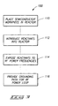
- a preferred semiconductor processing method is set forth in a flow diagram indicated generally at 100 in Fig. 3.
- a semiconductor workpiece such as wafer W (Fig. 1) is placed in reactor 10 and preferably upon second or susceptor electrode 18 as shown.
- the susceptor electrode supports the workpiece interiorly of the preferred reactor for subsequent processing.
- Gaseous reactants are introduced into the reactor at step 112 preferably through the shower head electrode 16.
- the reactants are exposed to at least two different RF power frequencies to a degree which is sufficient to effect deposition of a reactant product over the semiconductor workpiece.
- RF power of a first frequency is applied to shower head electrode 16 from high frequency RF power source 26. Additionally, a second frequency of RF power is applied to susceptor electrode 18 which supports semiconductor workpiece W.
- a grounding path is provided which leads to and defines a grounding point for the high frequency power loop developed or produced by first RF power source 26. The grounding point is preferably located at a remote location from other component connective lines. Such is in the chamber interior, such as on a portion of the chamber interior side wall which is maintained at ground.
- the grounding path includes a bypass or bandpass filter 38 which is configured for passing only frequencies of the higher of the two frequencies i.e. those generated or produced by the high frequency power source 26.
- the filter is advantageously configured for grounding the high frequency power source internally of the reactor which serves to reduce if not eliminate any interference with the thermocouple line 30 and RF power line 34 which extends through a common opening 13.
- advantages include better film adhesion, lower pinhole density, better step coverage especially in high aspect ratio topographies, and films or layers with better electrical properties. Additionally, in PECVD systems in which etching is performed, better compatibility with fine-line pattern transfer processes can be achieved. Other advantages will be evident to those of skill in the art.
Landscapes
- Chemical & Material Sciences (AREA)
- Engineering & Computer Science (AREA)
- Physics & Mathematics (AREA)
- Plasma & Fusion (AREA)
- Analytical Chemistry (AREA)
- Chemical Kinetics & Catalysis (AREA)
- General Chemical & Material Sciences (AREA)
- Materials Engineering (AREA)
- Mechanical Engineering (AREA)
- Metallurgy (AREA)
- Organic Chemistry (AREA)
- Chemical Vapour Deposition (AREA)
- Physical Or Chemical Processes And Apparatus (AREA)
- Details Of Rigid Or Semi-Rigid Containers (AREA)
Abstract
Description
Claims (8)
- A dual frequency plasma enhanced chemical vapor deposition reactor (10) comprising:a reactor interior surface (14) defining a processing chamber (12) with at least a portion of the interior surface (14) being grounded;a first frequency RF power source (26) configured to develop a first frequency power loop at least a portion of which passes within the chamber (12);a first electrode (16) inside the processing chamber (12) operably associated with the first frequency RF power source (26) and configured to be powered thereby,a second frequency RF power source (32) configured to develop RF power at frequencies which are lower than frequencies developed by the first frequency RF power source (26);a second electrode (18) inside the processing chamber (12) operably associated with the second frequency RF power source (26) and configured to be powered thereby; andgrounding means for the first frequency power loop, the reactor being characterized in that said first electrode (16) is a shower head electrode (16) configured to introduce reactants into the reactor (10); that said grounding means includes a grounding path within said chamber (12) grounded to said grounded interior chamber surface (14), and in that the grounding path includes a band pass filter, the band pass filter (38) being configured to pass only frequencies developed by the first frequency RF power source (26).
- A dual frequency plasma enhanced chemical vapor deposition reactor (10) as claimed in claim 1, characterized in that the second electrode (18) is configured for supporting at least one semiconductor workpiece (W) for processing internally of the chamber (12).
- A dual frequency plasma enhanced chemical vapor deposition reactor (10) as claimed in claim 1, characterized by a power line (34) connecting the second frequency RF power source (32) and the second electrode (18), a portion of the power line (34) defining at least a portion of the grounding path.
- A dual frequency plasma enhanced chemical vapor deposition reactor (10) as claimed in claim 1, characterized by:a conduit in the processing chamber (12) defining a path from inside the reactor (10) to outside the reactor (10);a power line (34) extending through the conduit and operably connecting the second electrode (18) and the second frequency RF power source (32);a temperature sensor (28) operably connected with the second electrode (18)and configured to provide temperature information relative to the second electrode (18); anda temperature sensor line (30) connected with the temperature sensor (28) and extending through the conduit to a point outside the reactor (10).
- A dual frequency plasma enhanced chemical vapor deposition reactor (10) as claimed in claim 1, characterized by:a temperature sensor (28) operably connected with the second electrode (18) and configured to provide temperature information relative to the second electrode (18); anda temperature sensor line (30) coupled to the temperature sensor (28) and extending to a point outside of the reactor.
- A semiconductor processing method (100) of effecting plasma enhanced chemical vapor deposition comprising the steps of:supporting (110) with a susceptor electrode (18) at least one semiconductor workpiece (W) interiorly of a parallel plate plasma enhanced chemical vapor deposition reactor (10);introducing reactants (112) into the reactor (10) through a shower head electrode (16); andexposing (114) the reactants to at least two different RF power frequencies to a degree sufficient to effect deposition of a reactant product over the semiconductor workpiece (W), the exposing (114) comprising:grounding (116) to a grounded interior surface (14) of the reactor chamber, an RF power loop of the higher of the two RF power frequencies, said grounding (116) comprising providing a grounding path within said chamber, said path including a bandpass filter (38) configured to pass only frequencies of the power loop which is grounded.
- A semiconductor processing method (100) as claimed in claim 6, characterized in that:the two different RF power frequencies are produced by two different RF power sources (26, 32), a first of the RF power sources (26) developing RF power at frequencies which are higher than RF power developed by a second of the RF power sources (32), the first RF power source (26) being coupled with the shower head electrode (16), and the second of the power sources (32) being coupled with the susceptor electrode (18);the RF power loop which is grounded corresponds to the higher of the two frequencies; andthe grounding (116) comprises grounding (116) the RF power loop of the higher of the two frequencies.
- A semiconductor processing method (100) as claimed in claim 6, characterized by operatively coupling a thermocouple (28) to the susceptor electrode (18).
Applications Claiming Priority (3)
| Application Number | Priority Date | Filing Date | Title |
|---|---|---|---|
| US09/026,566 US6112697A (en) | 1998-02-19 | 1998-02-19 | RF powered plasma enhanced chemical vapor deposition reactor and methods |
| US26566 | 1998-02-19 | ||
| PCT/US1999/003229 WO1999043017A1 (en) | 1998-02-19 | 1999-02-16 | Rf powered plasma enhanced chemical vapor deposition reactor and methods |
Publications (2)
| Publication Number | Publication Date |
|---|---|
| EP1057207A1 EP1057207A1 (en) | 2000-12-06 |
| EP1057207B1 true EP1057207B1 (en) | 2004-06-16 |
Family
ID=21832548
Family Applications (1)
| Application Number | Title | Priority Date | Filing Date |
|---|---|---|---|
| EP99934367A Expired - Lifetime EP1057207B1 (en) | 1998-02-19 | 1999-02-16 | Rf powered plasma enhanced chemical vapor deposition reactor and methods |
Country Status (9)
| Country | Link |
|---|---|
| US (2) | US6112697A (en) |
| EP (1) | EP1057207B1 (en) |
| JP (2) | JP3822055B2 (en) |
| KR (1) | KR100388529B1 (en) |
| AT (1) | ATE269586T1 (en) |
| AU (1) | AU3293999A (en) |
| DE (1) | DE69918063T2 (en) |
| TW (1) | TW523830B (en) |
| WO (1) | WO1999043017A1 (en) |
Families Citing this family (46)
| Publication number | Priority date | Publication date | Assignee | Title |
|---|---|---|---|---|
| FR2806324B1 (en) * | 2000-03-15 | 2002-09-27 | Air Liquide | METHOD AND DEVICE FOR IMPLEMENTING A CHEMICAL REACTION AND SURFACE TREATMENT METHOD USING SUCH METHOD AND DEVICE |
| US6857387B1 (en) | 2000-05-03 | 2005-02-22 | Applied Materials, Inc. | Multiple frequency plasma chamber with grounding capacitor at cathode |
| US6562684B1 (en) | 2000-08-30 | 2003-05-13 | Micron Technology, Inc. | Methods of forming dielectric materials |
| US6782337B2 (en) | 2000-09-20 | 2004-08-24 | Kla-Tencor Technologies Corp. | Methods and systems for determining a critical dimension an a presence of defects on a specimen |
| US7196782B2 (en) | 2000-09-20 | 2007-03-27 | Kla-Tencor Technologies Corp. | Methods and systems for determining a thin film characteristic and an electrical property of a specimen |
| US6673637B2 (en) | 2000-09-20 | 2004-01-06 | Kla-Tencor Technologies | Methods and systems for determining a presence of macro defects and overlay of a specimen |
| US6891627B1 (en) | 2000-09-20 | 2005-05-10 | Kla-Tencor Technologies Corp. | Methods and systems for determining a critical dimension and overlay of a specimen |
| US6694284B1 (en) | 2000-09-20 | 2004-02-17 | Kla-Tencor Technologies Corp. | Methods and systems for determining at least four properties of a specimen |
| US6812045B1 (en) | 2000-09-20 | 2004-11-02 | Kla-Tencor, Inc. | Methods and systems for determining a characteristic of a specimen prior to, during, or subsequent to ion implantation |
| JP4877884B2 (en) * | 2001-01-25 | 2012-02-15 | 東京エレクトロン株式会社 | Plasma processing equipment |
| WO2002095800A2 (en) * | 2001-05-22 | 2002-11-28 | Reflectivity, Inc. | A method for making a micromechanical device by removing a sacrificial layer with multiple sequential etchants |
| US20040025791A1 (en) * | 2002-08-09 | 2004-02-12 | Applied Materials, Inc. | Etch chamber with dual frequency biasing sources and a single frequency plasma generating source |
| US6838012B2 (en) * | 2002-10-31 | 2005-01-04 | Lam Research Corporation | Methods for etching dielectric materials |
| US20040188240A1 (en) * | 2003-03-28 | 2004-09-30 | Taiwan Semiconductor Manufacturing Co., Ltd. | Process for in-situ nitridation of salicides |
| GB0309932D0 (en) * | 2003-04-30 | 2003-06-04 | Boc Group Plc | Apparatus and method for forming a plasma |
| US7431857B2 (en) * | 2003-08-15 | 2008-10-07 | Applied Materials, Inc. | Plasma generation and control using a dual frequency RF source |
| US20050118541A1 (en) * | 2003-11-28 | 2005-06-02 | Applied Materials, Inc. | Maintenance of photoresist adhesion and activity on the surface of dielectric ARCS for 90 nm feature sizes |
| US7829471B2 (en) | 2005-07-29 | 2010-11-09 | Applied Materials, Inc. | Cluster tool and method for process integration in manufacturing of a photomask |
| US20070031609A1 (en) | 2005-07-29 | 2007-02-08 | Ajay Kumar | Chemical vapor deposition chamber with dual frequency bias and method for manufacturing a photomask using the same |
| US7375038B2 (en) | 2005-09-28 | 2008-05-20 | Applied Materials, Inc. | Method for plasma etching a chromium layer through a carbon hard mask suitable for photomask fabrication |
| US7695633B2 (en) * | 2005-10-18 | 2010-04-13 | Applied Materials, Inc. | Independent control of ion density, ion energy distribution and ion dissociation in a plasma reactor |
| US20070246162A1 (en) * | 2006-04-24 | 2007-10-25 | Applied Materials, Inc. | Plasma reactor apparatus with an inductive plasma source and a VHF capacitively coupled plasma source with variable frequency |
| US7727413B2 (en) * | 2006-04-24 | 2010-06-01 | Applied Materials, Inc. | Dual plasma source process using a variable frequency capacitively coupled source to control plasma ion density |
| US20070245958A1 (en) * | 2006-04-24 | 2007-10-25 | Applied Materials, Inc. | Dual plasma source process using a variable frequency capacitively coupled source for controlling ion radial distribution |
| US20070245960A1 (en) * | 2006-04-24 | 2007-10-25 | Applied Materials, Inc. | Process using combined capacitively and inductively coupled plasma sources for controlling plasma ion density |
| US20070246163A1 (en) * | 2006-04-24 | 2007-10-25 | Applied Materials, Inc. | Plasma reactor apparatus with independent capacitive and inductive plasma sources |
| US20070246443A1 (en) * | 2006-04-24 | 2007-10-25 | Applied Materials, Inc. | Process using combined capacitively and inductively coupled plasma process for controlling plasma ion dissociation |
| US20070245961A1 (en) * | 2006-04-24 | 2007-10-25 | Applied Materials, Inc. | Dual plasma source process using a variable frequency capacitively coupled source for controlling plasma ion dissociation |
| US7645357B2 (en) * | 2006-04-24 | 2010-01-12 | Applied Materials, Inc. | Plasma reactor apparatus with a VHF capacitively coupled plasma source of variable frequency |
| US20070246161A1 (en) * | 2006-04-24 | 2007-10-25 | Applied Materials, Inc. | Plasma reactor apparatus with a toroidal plasma source and a VHF capacitively coupled plasma source with variable frequency |
| US7780864B2 (en) | 2006-04-24 | 2010-08-24 | Applied Materials, Inc. | Process using combined capacitively and inductively coupled plasma sources for controlling plasma ion radial distribution |
| US8673080B2 (en) | 2007-10-16 | 2014-03-18 | Novellus Systems, Inc. | Temperature controlled showerhead |
| US20090104541A1 (en) * | 2007-10-23 | 2009-04-23 | Eui Kyoon Kim | Plasma surface treatment to prevent pattern collapse in immersion lithography |
| US20090188625A1 (en) * | 2008-01-28 | 2009-07-30 | Carducci James D | Etching chamber having flow equalizer and lower liner |
| US8637794B2 (en) | 2009-10-21 | 2014-01-28 | Lam Research Corporation | Heating plate with planar heating zones for semiconductor processing |
| US9034142B2 (en) * | 2009-12-18 | 2015-05-19 | Novellus Systems, Inc. | Temperature controlled showerhead for high temperature operations |
| KR101415552B1 (en) * | 2009-12-21 | 2014-07-07 | 주식회사 미코 | Ground structure, and heater and chemical vapor deposition apparatus including the same |
| JP5730521B2 (en) | 2010-09-08 | 2015-06-10 | 株式会社日立ハイテクノロジーズ | Heat treatment equipment |
| US8791392B2 (en) | 2010-10-22 | 2014-07-29 | Lam Research Corporation | Methods of fault detection for multiplexed heater array |
| KR101937115B1 (en) | 2011-03-04 | 2019-01-09 | 노벨러스 시스템즈, 인코포레이티드 | Hybrid ceramic showerhead |
| US8618446B2 (en) | 2011-06-30 | 2013-12-31 | Applied Materials, Inc. | Substrate support with substrate heater and symmetric RF return |
| US10741365B2 (en) | 2014-05-05 | 2020-08-11 | Lam Research Corporation | Low volume showerhead with porous baffle |
| US10378107B2 (en) | 2015-05-22 | 2019-08-13 | Lam Research Corporation | Low volume showerhead with faceplate holes for improved flow uniformity |
| US10023959B2 (en) | 2015-05-26 | 2018-07-17 | Lam Research Corporation | Anti-transient showerhead |
| US10332810B2 (en) | 2016-10-24 | 2019-06-25 | Kla-Tencor Corp. | Process modules integrated into a metrology and/or inspection tool |
| US20200098562A1 (en) * | 2018-09-26 | 2020-03-26 | Lam Research Corporation | Dual frequency silane-based silicon dioxide deposition to minimize film instability |
Family Cites Families (35)
| Publication number | Priority date | Publication date | Assignee | Title |
|---|---|---|---|---|
| US4585516A (en) * | 1985-03-04 | 1986-04-29 | Tegal Corporation | Variable duty cycle, multiple frequency, plasma reactor |
| US5230931A (en) * | 1987-08-10 | 1993-07-27 | Semiconductor Energy Laboratory Co., Ltd. | Plasma-assisted cvd of carbonaceous films by using a bias voltage |
| US4887005A (en) | 1987-09-15 | 1989-12-12 | Rough J Kirkwood H | Multiple electrode plasma reactor power distribution system |
| JP2629871B2 (en) | 1988-08-29 | 1997-07-16 | スズキ株式会社 | Transmission for vehicles |
| JPH02213480A (en) * | 1989-02-14 | 1990-08-24 | Nippon Light Metal Co Ltd | Aluminum electrode for generating high frequency plasma |
| JPH02298024A (en) * | 1989-05-12 | 1990-12-10 | Tadahiro Omi | Reactive ion etching apparatus |
| JP3016821B2 (en) * | 1990-06-15 | 2000-03-06 | 東京エレクトロン株式会社 | Plasma processing method |
| FR2663806A1 (en) * | 1990-06-25 | 1991-12-27 | Commissariat Energie Atomique | Plasma reactor of the triode type, usable in particular for etching, deposition or cleaning of surfaces |
| DE4025396A1 (en) * | 1990-08-10 | 1992-02-13 | Leybold Ag | DEVICE FOR PRODUCING A PLASMA |
| US5052339A (en) * | 1990-10-16 | 1991-10-01 | Air Products And Chemicals, Inc. | Radio frequency plasma enhanced chemical vapor deposition process and reactor |
| JPH04362091A (en) * | 1991-06-05 | 1992-12-15 | Mitsubishi Heavy Ind Ltd | Plasma chemical vapor deposition apparatus |
| US5260236A (en) * | 1991-06-07 | 1993-11-09 | Intel Corporation | UV transparent oxynitride deposition in single wafer PECVD system |
| JPH05175163A (en) * | 1991-12-24 | 1993-07-13 | Mitsubishi Electric Corp | Plasma processing device |
| EP0849766A3 (en) * | 1992-01-24 | 1998-10-14 | Applied Materials, Inc. | Etch process |
| JP3122228B2 (en) * | 1992-05-13 | 2001-01-09 | 忠弘 大見 | Process equipment |
| US5567267A (en) * | 1992-11-20 | 1996-10-22 | Tokyo Electron Limited | Method of controlling temperature of susceptor |
| US5665167A (en) * | 1993-02-16 | 1997-09-09 | Tokyo Electron Kabushiki Kaisha | Plasma treatment apparatus having a workpiece-side electrode grounding circuit |
| JP3351843B2 (en) * | 1993-02-24 | 2002-12-03 | 忠弘 大見 | Film formation method |
| US5439524A (en) * | 1993-04-05 | 1995-08-08 | Vlsi Technology, Inc. | Plasma processing apparatus |
| US5433786A (en) * | 1993-08-27 | 1995-07-18 | The Dow Chemical Company | Apparatus for plasma enhanced chemical vapor deposition comprising shower head electrode with magnet disposed therein |
| US5468296A (en) * | 1993-12-17 | 1995-11-21 | Lsi Logic Corporation | Apparatus for igniting low pressure inductively coupled plasma |
| US5900103A (en) * | 1994-04-20 | 1999-05-04 | Tokyo Electron Limited | Plasma treatment method and apparatus |
| DE69512371T2 (en) * | 1994-05-13 | 2000-04-06 | Applied Materials Inc | MAGNETICALLY IMPROVED MULTIPLE CAPACITIVE PLASMA GENERATING DEVICE AND METHOD |
| US5607542A (en) * | 1994-11-01 | 1997-03-04 | Applied Materials Inc. | Inductively enhanced reactive ion etching |
| US5716534A (en) * | 1994-12-05 | 1998-02-10 | Tokyo Electron Limited | Plasma processing method and plasma etching method |
| US5605637A (en) * | 1994-12-15 | 1997-02-25 | Applied Materials Inc. | Adjustable dc bias control in a plasma reactor |
| US5710486A (en) * | 1995-05-08 | 1998-01-20 | Applied Materials, Inc. | Inductively and multi-capacitively coupled plasma reactor |
| EP0831679B1 (en) | 1995-06-05 | 2008-10-01 | Musashino Kikai Co., Ltd. | Power supply for multielectrode discharge |
| TW434745B (en) * | 1995-06-07 | 2001-05-16 | Tokyo Electron Ltd | Plasma processing apparatus |
| US5656123A (en) * | 1995-06-07 | 1997-08-12 | Varian Associates, Inc. | Dual-frequency capacitively-coupled plasma reactor for materials processing |
| JP2814370B2 (en) * | 1995-06-18 | 1998-10-22 | 東京エレクトロン株式会社 | Plasma processing equipment |
| US5865937A (en) * | 1995-08-21 | 1999-02-02 | Applied Materials, Inc. | Broad-band adjustable power ratio phase-inverting plasma reactor |
| EP0776991B1 (en) * | 1995-12-05 | 2002-02-06 | Applied Materials, Inc. | Plasma annealing of thin films |
| JPH09167755A (en) * | 1995-12-15 | 1997-06-24 | Nec Corp | Plasma oxide film processor |
| US5981899A (en) | 1997-01-17 | 1999-11-09 | Balzers Aktiengesellschaft | Capacitively coupled RF-plasma reactor |
-
1998
- 1998-02-19 US US09/026,566 patent/US6112697A/en not_active Expired - Lifetime
-
1999
- 1999-02-16 KR KR10-2000-7008726A patent/KR100388529B1/en not_active IP Right Cessation
- 1999-02-16 WO PCT/US1999/003229 patent/WO1999043017A1/en active IP Right Grant
- 1999-02-16 EP EP99934367A patent/EP1057207B1/en not_active Expired - Lifetime
- 1999-02-16 DE DE69918063T patent/DE69918063T2/en not_active Expired - Lifetime
- 1999-02-16 AU AU32939/99A patent/AU3293999A/en not_active Abandoned
- 1999-02-16 AT AT99934367T patent/ATE269586T1/en not_active IP Right Cessation
- 1999-02-16 JP JP2000532862A patent/JP3822055B2/en not_active Expired - Fee Related
- 1999-03-15 TW TW088102447A patent/TW523830B/en active
-
2000
- 2000-06-19 US US09/597,659 patent/US6227141B1/en not_active Expired - Lifetime
-
2003
- 2003-05-26 JP JP2003147766A patent/JP4217883B2/en not_active Expired - Fee Related
Also Published As
| Publication number | Publication date |
|---|---|
| WO1999043017A1 (en) | 1999-08-26 |
| ATE269586T1 (en) | 2004-07-15 |
| JP3822055B2 (en) | 2006-09-13 |
| KR20010040831A (en) | 2001-05-15 |
| EP1057207A1 (en) | 2000-12-06 |
| US6112697A (en) | 2000-09-05 |
| AU3293999A (en) | 1999-09-06 |
| US6227141B1 (en) | 2001-05-08 |
| JP2002504748A (en) | 2002-02-12 |
| JP4217883B2 (en) | 2009-02-04 |
| DE69918063T2 (en) | 2005-06-30 |
| KR100388529B1 (en) | 2003-06-25 |
| TW523830B (en) | 2003-03-11 |
| JP2004006885A (en) | 2004-01-08 |
| DE69918063D1 (en) | 2004-07-22 |
Similar Documents
| Publication | Publication Date | Title |
|---|---|---|
| EP1057207B1 (en) | Rf powered plasma enhanced chemical vapor deposition reactor and methods | |
| US6395128B2 (en) | RF powered plasma enhanced chemical vapor deposition reactor and methods of effecting plasma enhanced chemical vapor deposition | |
| US5496410A (en) | Plasma processing apparatus and method of processing substrates by using same apparatus | |
| EP0026604B1 (en) | A method of vapour phase growth and apparatus therefor | |
| US5626679A (en) | Method and apparatus for preparing a silicon oxide film | |
| US5015330A (en) | Film forming method and film forming device | |
| US6026762A (en) | Apparatus for improved remote microwave plasma source for use with substrate processing systems | |
| EP0792947B1 (en) | Process using an inductively coupled plasma reactor | |
| US20050252885A1 (en) | Plasma etching method and apparatus | |
| KR100727205B1 (en) | Plasma deposition method and system | |
| US20040200413A1 (en) | Chemical vapor deposition apparatus | |
| KR100377096B1 (en) | Semiconductor fabricating apparatus having improved shower head | |
| US6626186B1 (en) | Method for stabilizing the internal surface of a PECVD process chamber | |
| US20010042513A1 (en) | Apparatus for improved remote microwave plasma source for use with substrate processing systems | |
| JPS62210623A (en) | Electrode for vapor phase reactor | |
| JP3147769B2 (en) | Plasma processing apparatus and processing method | |
| JPH09289179A (en) | Cleaning method of cvd-ti film forming chamber | |
| JP4168126B2 (en) | Method for stabilizing the inner surface of a plasma enhanced chemical vapor deposition chamber | |
| JPH1112742A (en) | Cvd device, and its cleaning method | |
| JPH10242116A (en) | Parallel flat plate type rie apparatus | |
| JP2628529B2 (en) | Plasma CVD equipment | |
| KR20040018835A (en) | Sample processing apparatus and sample processing system | |
| JPH02115371A (en) | Formation of thin film by plasma cvd |
Legal Events
| Date | Code | Title | Description |
|---|---|---|---|
| PUAI | Public reference made under article 153(3) epc to a published international application that has entered the european phase |
Free format text: ORIGINAL CODE: 0009012 |
|
| 17P | Request for examination filed |
Effective date: 20000721 |
|
| AK | Designated contracting states |
Kind code of ref document: A1 Designated state(s): AT BE CH CY DE DK ES FI FR GB GR IE IT LI LU MC NL PT SE |
|
| 17Q | First examination report despatched |
Effective date: 20020411 |
|
| GRAP | Despatch of communication of intention to grant a patent |
Free format text: ORIGINAL CODE: EPIDOSNIGR1 |
|
| GRAS | Grant fee paid |
Free format text: ORIGINAL CODE: EPIDOSNIGR3 |
|
| GRAA | (expected) grant |
Free format text: ORIGINAL CODE: 0009210 |
|
| AK | Designated contracting states |
Kind code of ref document: B1 Designated state(s): AT BE CH CY DE DK ES FI FR GB GR IE IT LI LU MC NL PT SE |
|
| PG25 | Lapsed in a contracting state [announced via postgrant information from national office to epo] |
Ref country code: NL Free format text: LAPSE BECAUSE OF FAILURE TO SUBMIT A TRANSLATION OF THE DESCRIPTION OR TO PAY THE FEE WITHIN THE PRESCRIBED TIME-LIMIT Effective date: 20040616 Ref country code: LI Free format text: LAPSE BECAUSE OF FAILURE TO SUBMIT A TRANSLATION OF THE DESCRIPTION OR TO PAY THE FEE WITHIN THE PRESCRIBED TIME-LIMIT Effective date: 20040616 Ref country code: FI Free format text: LAPSE BECAUSE OF FAILURE TO SUBMIT A TRANSLATION OF THE DESCRIPTION OR TO PAY THE FEE WITHIN THE PRESCRIBED TIME-LIMIT Effective date: 20040616 Ref country code: CH Free format text: LAPSE BECAUSE OF FAILURE TO SUBMIT A TRANSLATION OF THE DESCRIPTION OR TO PAY THE FEE WITHIN THE PRESCRIBED TIME-LIMIT Effective date: 20040616 Ref country code: BE Free format text: LAPSE BECAUSE OF FAILURE TO SUBMIT A TRANSLATION OF THE DESCRIPTION OR TO PAY THE FEE WITHIN THE PRESCRIBED TIME-LIMIT Effective date: 20040616 Ref country code: AT Free format text: LAPSE BECAUSE OF FAILURE TO SUBMIT A TRANSLATION OF THE DESCRIPTION OR TO PAY THE FEE WITHIN THE PRESCRIBED TIME-LIMIT Effective date: 20040616 |
|
| REG | Reference to a national code |
Ref country code: GB Ref legal event code: FG4D |
|
| REG | Reference to a national code |
Ref country code: CH Ref legal event code: EP |
|
| REF | Corresponds to: |
Ref document number: 69918063 Country of ref document: DE Date of ref document: 20040722 Kind code of ref document: P |
|
| REG | Reference to a national code |
Ref country code: IE Ref legal event code: FG4D |
|
| PG25 | Lapsed in a contracting state [announced via postgrant information from national office to epo] |
Ref country code: SE Free format text: LAPSE BECAUSE OF FAILURE TO SUBMIT A TRANSLATION OF THE DESCRIPTION OR TO PAY THE FEE WITHIN THE PRESCRIBED TIME-LIMIT Effective date: 20040916 Ref country code: GR Free format text: LAPSE BECAUSE OF FAILURE TO SUBMIT A TRANSLATION OF THE DESCRIPTION OR TO PAY THE FEE WITHIN THE PRESCRIBED TIME-LIMIT Effective date: 20040916 Ref country code: DK Free format text: LAPSE BECAUSE OF FAILURE TO SUBMIT A TRANSLATION OF THE DESCRIPTION OR TO PAY THE FEE WITHIN THE PRESCRIBED TIME-LIMIT Effective date: 20040916 |
|
| PG25 | Lapsed in a contracting state [announced via postgrant information from national office to epo] |
Ref country code: ES Free format text: LAPSE BECAUSE OF FAILURE TO SUBMIT A TRANSLATION OF THE DESCRIPTION OR TO PAY THE FEE WITHIN THE PRESCRIBED TIME-LIMIT Effective date: 20040927 |
|
| NLV1 | Nl: lapsed or annulled due to failure to fulfill the requirements of art. 29p and 29m of the patents act | ||
| REG | Reference to a national code |
Ref country code: CH Ref legal event code: PL |
|
| ET | Fr: translation filed | ||
| PG25 | Lapsed in a contracting state [announced via postgrant information from national office to epo] |
Ref country code: LU Free format text: LAPSE BECAUSE OF NON-PAYMENT OF DUE FEES Effective date: 20050216 Ref country code: IE Free format text: LAPSE BECAUSE OF NON-PAYMENT OF DUE FEES Effective date: 20050216 Ref country code: CY Free format text: LAPSE BECAUSE OF FAILURE TO SUBMIT A TRANSLATION OF THE DESCRIPTION OR TO PAY THE FEE WITHIN THE PRESCRIBED TIME-LIMIT Effective date: 20050216 |
|
| PG25 | Lapsed in a contracting state [announced via postgrant information from national office to epo] |
Ref country code: MC Free format text: LAPSE BECAUSE OF NON-PAYMENT OF DUE FEES Effective date: 20050228 |
|
| PLBE | No opposition filed within time limit |
Free format text: ORIGINAL CODE: 0009261 |
|
| STAA | Information on the status of an ep patent application or granted ep patent |
Free format text: STATUS: NO OPPOSITION FILED WITHIN TIME LIMIT |
|
| 26N | No opposition filed |
Effective date: 20050317 |
|
| REG | Reference to a national code |
Ref country code: IE Ref legal event code: MM4A |
|
| PG25 | Lapsed in a contracting state [announced via postgrant information from national office to epo] |
Ref country code: PT Free format text: LAPSE BECAUSE OF NON-PAYMENT OF DUE FEES Effective date: 20041116 |
|
| PGFP | Annual fee paid to national office [announced via postgrant information from national office to epo] |
Ref country code: DE Payment date: 20110208 Year of fee payment: 13 Ref country code: IT Payment date: 20110216 Year of fee payment: 13 Ref country code: FR Payment date: 20110218 Year of fee payment: 13 |
|
| PGFP | Annual fee paid to national office [announced via postgrant information from national office to epo] |
Ref country code: GB Payment date: 20110216 Year of fee payment: 13 |
|
| GBPC | Gb: european patent ceased through non-payment of renewal fee |
Effective date: 20120216 |
|
| REG | Reference to a national code |
Ref country code: FR Ref legal event code: ST Effective date: 20121031 |
|
| PG25 | Lapsed in a contracting state [announced via postgrant information from national office to epo] |
Ref country code: IT Free format text: LAPSE BECAUSE OF NON-PAYMENT OF DUE FEES Effective date: 20120216 |
|
| REG | Reference to a national code |
Ref country code: DE Ref legal event code: R119 Ref document number: 69918063 Country of ref document: DE Effective date: 20120901 |
|
| PG25 | Lapsed in a contracting state [announced via postgrant information from national office to epo] |
Ref country code: FR Free format text: LAPSE BECAUSE OF NON-PAYMENT OF DUE FEES Effective date: 20120229 Ref country code: GB Free format text: LAPSE BECAUSE OF NON-PAYMENT OF DUE FEES Effective date: 20120216 |
|
| PG25 | Lapsed in a contracting state [announced via postgrant information from national office to epo] |
Ref country code: DE Free format text: LAPSE BECAUSE OF NON-PAYMENT OF DUE FEES Effective date: 20120901 |