EP1058111A2 - Optical inspection system and method - Google Patents
Optical inspection system and method Download PDFInfo
- Publication number
- EP1058111A2 EP1058111A2 EP00401435A EP00401435A EP1058111A2 EP 1058111 A2 EP1058111 A2 EP 1058111A2 EP 00401435 A EP00401435 A EP 00401435A EP 00401435 A EP00401435 A EP 00401435A EP 1058111 A2 EP1058111 A2 EP 1058111A2
- Authority
- EP
- European Patent Office
- Prior art keywords
- workpiece
- axis
- symmetry
- inspection
- optical assemblies
- Prior art date
- Legal status (The legal status is an assumption and is not a legal conclusion. Google has not performed a legal analysis and makes no representation as to the accuracy of the status listed.)
- Withdrawn
Links
Images


Classifications
-
- G—PHYSICS
- G01—MEASURING; TESTING
- G01N—INVESTIGATING OR ANALYSING MATERIALS BY DETERMINING THEIR CHEMICAL OR PHYSICAL PROPERTIES
- G01N21/00—Investigating or analysing materials by the use of optical means, i.e. using sub-millimetre waves, infrared, visible or ultraviolet light
- G01N21/84—Systems specially adapted for particular applications
- G01N21/88—Investigating the presence of flaws or contamination
- G01N21/95—Investigating the presence of flaws or contamination characterised by the material or shape of the object to be examined
- G01N21/9501—Semiconductor wafers
-
- G—PHYSICS
- G01—MEASURING; TESTING
- G01N—INVESTIGATING OR ANALYSING MATERIALS BY DETERMINING THEIR CHEMICAL OR PHYSICAL PROPERTIES
- G01N21/00—Investigating or analysing materials by the use of optical means, i.e. using sub-millimetre waves, infrared, visible or ultraviolet light
- G01N21/84—Systems specially adapted for particular applications
- G01N21/88—Investigating the presence of flaws or contamination
- G01N21/95—Investigating the presence of flaws or contamination characterised by the material or shape of the object to be examined
- G01N21/956—Inspecting patterns on the surface of objects
-
- G—PHYSICS
- G01—MEASURING; TESTING
- G01N—INVESTIGATING OR ANALYSING MATERIALS BY DETERMINING THEIR CHEMICAL OR PHYSICAL PROPERTIES
- G01N21/00—Investigating or analysing materials by the use of optical means, i.e. using sub-millimetre waves, infrared, visible or ultraviolet light
- G01N21/84—Systems specially adapted for particular applications
- G01N21/88—Investigating the presence of flaws or contamination
- G01N21/8806—Specially adapted optical and illumination features
- G01N2021/8822—Dark field detection
- G01N2021/8825—Separate detection of dark field and bright field
-
- G—PHYSICS
- G01—MEASURING; TESTING
- G01N—INVESTIGATING OR ANALYSING MATERIALS BY DETERMINING THEIR CHEMICAL OR PHYSICAL PROPERTIES
- G01N21/00—Investigating or analysing materials by the use of optical means, i.e. using sub-millimetre waves, infrared, visible or ultraviolet light
- G01N21/84—Systems specially adapted for particular applications
- G01N21/88—Investigating the presence of flaws or contamination
- G01N21/94—Investigating contamination, e.g. dust
-
- G—PHYSICS
- G01—MEASURING; TESTING
- G01N—INVESTIGATING OR ANALYSING MATERIALS BY DETERMINING THEIR CHEMICAL OR PHYSICAL PROPERTIES
- G01N2201/00—Features of devices classified in G01N21/00
- G01N2201/06—Illumination; Optics
- G01N2201/063—Illuminating optical parts
- G01N2201/0635—Structured illumination, e.g. with grating
Definitions
- the present invention is in the field of automatic inspection techniques, and relates to an optical inspection method and system, particularly useful for inspecting semiconductor wafers progressing on a production line.
- the manufacture of semiconductor devices consists of a multi-staged process requiring wafers progressing on a production line to be inspected between sequential manufacturing steps.
- One of the principle processes in the manufacture of semiconductor devices is the photolithography process. It consists of patterning the wafer's surface in accordance with the active elements of semiconductor devices to be manufactured.
- the photolithography process includes the following main operational steps:
- the wafer prior to the photolithography process, the wafer is prepared for the deposition of one or more layers. After the completion of the photolithography process, the uppermost layer of the wafer is etched. Then a new layer is deposited, in order to start the photolithography and etching operations again. In this repetitive manner, a multi-layer semiconductor wafer is produced.
- Fig. 1 illustrates a block diagram of a typical photocluster 1 used for performing the photolithography process in semiconductor fabrication plants (FABs).
- the photocluster 1 (or link) is composed of two main parts: a phototrack 2 and an exposure tool 4.
- the phototrack 2 includes a coater track 6 associated with a cassette load station 6a , and a developer track 8 associated with a cassette unload station 8a .
- a load/unload robot R is mounted for movement within the photocluster 1 for conveying wafers W to and from the photocluster tools.
- the coater track 6 , the exposure tool 4 and the development track 8 are tightly joined together in order to minimize process variability and any potential risk of contamination during photolithography, which is a super sensitive process.
- a manual inspection technique is conventionally used for inspecting the wafers for so-called macro lithography defects, such as scratches or foreign particles of dust and dirt.
- macro defects are considered as defects having tenths of micrometers in size.
- the manual inspection technique utilizes the visual examination of the wafer's surface by an operator using intense light and magnification. This inspection is inconsistent and unreliable, since the results vary significantly amongst operators, due to the wafer's complexity and depending on the operators' experience. About 80% of the photo-related defects remain undetected. Manual inspection has low throughput, and could not be performed within the FAB tools. Manual inspection is not cost effective.
- the area sensor based technique utilizes a so-called step-and-repeat mode of operation, wherein the camera and the wafer are mounted for movement relative to each other to cover the entire surface of the wafer. More specifically, the camera and the wafer are moved step-by-step, and images are acquired upon the camera or the wafer stops.
- This technique requires a quite complicated mechanical stage providing movement along two mutually perpendicular axes. Additionally, it results in low throughput due to a great number of movement steps, and requires an additional footprint for performing such a two-dimensional movement.
- Machine vision systems having multiple cameras have been developed, being disclosed, for example, in U.S. Patent No. 5,768,443.
- images are acquired simultaneously by a plurality of cameras.
- the fields of view of the cameras cover a relatively large area of the wafer under inspection, thereby increasing the throughput of the system, as compared to the techniques utilizing a single line or area sensor.
- this patent does not present any example of the cameras' arrangement, which would be useful in an integrated inspection.
- An inspection machine should be inexpensive, simple to erect and maintain, and should have a small footprint (like a wafer cassette) to meet the requirements of the integrated inspection.
- Laser inspection systems have been developed which utilize various types of scanners and collectors for scanning the wafer's surface during the translational movement and for collecting light reflective and scattered from the surface. Such systems are disclosed, for example, in U.S. Patent Nos. 4,630,276; 5,108,176; 5,127,726 and 5,712,701. Unfortunately, these systems are complicated and expensive. Since they use monochromatic laser illumination, they are non-effective and insufficient for the inspection of developed photoresist for macro defects.
- the optical inspection system may be integrated into the production line. It is simple, inexpensive and compact, and provides for inspection with a high throughput of workpieces.
- a semiconductor wafer is typically a substantially flat workpiece, having an axis of symmetry (i.e. is round). Consequentially, one half of the wafer can be inspected by appropriately moving respective parts of a scanning apparatus above it, and, upon rotating the wafer about its axis of symmetry by 180°, inspecting the other half of the wafer.
- suitable mechanics should be provided for moving the respective components of the scanning apparatus solely within an inspection area equal to the half of the wafer, rather than moving them above the entire wafer, or moving both the respective components and the wafer relative to each other.
- a plurality of optical assemblies is mounted for movement above the wafer within the inspection area, the optical assemblies being aligned in a line parallel to the axis of symmetry of the wafer between the opposite sides thereof.
- a plurality of sensors is provided, each sensor being associated with a corresponding one of the plurality of optical assemblies.
- an optical inspection system for detecting defects on a substantially flat workpiece having an axis of symmetry, the system comprising a stage supporting said workpiece in an inspection plane, and a scanning apparatus accommodated above said workpiece, wherein:
- the illumination assembly may operate in bright-field illumination mode.
- it comprises a plurality of stationary mounted light sources aligned corresponding to the alignment of the optical assemblies, each incident radiation component being directed on the corresponding optical assembly, which, in turn, directs it onto the corresponding region of the workpiece.
- the illumination assembly may operate in a dark-filed illumination mode.
- it includes either a plurality of light sources, each accommodated in the vicinity of the corresponding optical assembly, or an elongated light source, extending along the optical assemblies in the proximity thereof.
- This "dark-field" illumination assembly is mounted for movement together with the optical assemblies. If the dark-field light illumination is used in addition to the bright-field illumination, the operation of the stationary mounted light sources and the operation of the movable light sources are time separated.
- the stationary mounted light sources may be continuously operated, while the movable light sources are selectively actuated to inspect only those locations on the workpiece where either a potential defect has been detected during the bright-field mode, or a real defect is expected.
- the area sensors may be arranged in a line parallel to the axis of symmetry and associated with the optical assemblies, so as to move together with the optical assemblies.
- the area sensors may be arranged in two parallel lines, parallel to the axis of symmetry, wherein each two adjacent sensors are displaced from each other along two mutually perpendicular axes.
- an additional light directing assembly is provided for receiving the components of the returned radiation ensuing from the optical assemblies, and directing them onto to the area sensors.
- a photolithography tools arrangement for processing a stream of substantial flat workpieces progressing on a production line, which tools arrangement comprises an optical inspection system constructed as described above.
- a method for inspecting a substantial flat workpiece having an axis of symmetry comprising the steps of:
- the present invention is used for inspecting wafers progressing within a photolithography tools set-up, and is therefore described below with respect to this application.
- Fig. 1 illustrates the configuration of the conventional photocluster 1 , which comprises the phototrack 2 and the exposure tool 4 , wherein the photo track is composed of the water track 6 and the developer track 8 .
- the water and developer tracks have their associated cassette load and unload stations 6a and 8a , respectively.
- the cassettes containing wafers are supplied to the phototrack 2 , being loaded from the station 6a onto the coater track 6 .
- a photoresist material is deposited onto the wafer's surface, and then the robot R transmits the coated wafer to the exposure tool 4 .
- the photoresist coating is exposed to light through a mask having a predetermined pattern to produce a latent image of the mask on the photoresist coating. Thereafter, the robot R transmits the wafer to the developer track 8 for developing the latent image.
- a photocluster 10 (constituting a photolithography tools arrangement) constructed according to one example of the invention.
- the same reference numbers are used for identifying those components which are common in the photoclusters 1 and 10 , to facilitate understanding.
- the photocluster 10 is constructed generally similar to the conventional photocluster 1 , but comprises an optical inspection system 12 , constructed and operated according to the invention, as will be described further below.
- the optical inspection system 12 is compact so as to be easily installed within the conventionally designed photocluster, enabling the use of the same robot R for feeding and discharging the wafers to and from the inspection system 12 .
- the system 12 may be dimensioned and shaped similar to that of the conventional cassette.
- the exact location of the inspection system 12 within the photocluster is selected in accordance with the considerations and circumstances of a specific manufacturer, an available foot-print inside the phototrack and the FAB considerations. Since the inspection system 12 is extremely compact, it can be positioned at a cassette location in the unloading area, or any other location accessible for the load/unload robot R .
- Fig. 2b illustrates a photolithography tools arrangement 14 , constructed according to another example of the invention.
- the arrangement 14 utilizes the photocluster 1 and the optical inspection system 12 , which is installed as a stand-alone unit within the photolithography tools arrangement 14 similar to the wafers' load/unload cassette station 15 .
- the robot R conveys wafers from the cassette 15 to the inspection system 12 and returns the inspected wafers back to the cassette station 15 , and supplies and discharges wafers to and from the photocluster 1 .
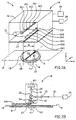
- Fig. 3a illustrates the main constructional parts of the optical inspection system 12 , constructed according to one embodiment of the invention.
- the inspection system 12 comprises a scanning apparatus 16 for inspecting a wafer W located on a support stage 18 , which supports the wafer W in an inspection plane IP .
- the wafer W has an axis of its symmetry OP defining half-parts P 1 and P 2 of the wafer W at opposite sides of the axis OP .
- Coupled to the stage 18 is a first drive mechanism D 1 for driving the rotational movement of the stage 18 within a plane parallel to the inspection plane IP .
- the scanning apparatus 16 inspects the wafer W within an inspection area IA defined by the half P 1 of the wafer, as will be described more specifically further below. Then, the drive mechanism D 1 operates to rotate the stage 18 by 180°, thereby locating the other half P 2 of the wafer within the inspection area IA .
- the scanning apparatus 16 comprises a sealed housing 22 containing a plurality of optical assemblies, for example five optical assemblies OA 1 -OA 5 , and a corresponding plurality of area sensors AS 1 -AS 5 .
- An illumination assembly 24 and a control unit 26 are accommodated outside the housing 22 .
- the housing 22 is formed with an optically transparent bottom portion 22a (i.e., window) substantially covering the inspection area IA (one half of the wafer).
- a second drive mechanism D 2 is accommodated inside the housing so as to be outside the inspection area IA .
- the drive mechanism D 2 is associated with the optical assemblies OA 1 -OA 5 and with the area sensors AS 1 -AS 5 for driving a reciprocation movement thereof along the X -axis within the inspection area IA .
- a suitable guiding assembly is provided for slidingly supporting the moving parts (i.e., optical assemblies and area sensors) inside the housing 22 .
- the optical assemblies OA 1 -OA 5 are accommodated above the window 22a being aligned along the Y -axis parallel to the axis of symmetry OP in a spaced-apart parallel relationship between the opposite sides of the wafer.
- the sensors AS 1 -AS 5 are arranged like a "rule" extending along the Y -axis and spaced from the optical assemblies along the Z -axis.
- the construction and operation of the control unit 26 do not form part of the present invention and may be of any known suitable kind, and therefore need not be specifically described, except to note the following.
- the control unit 26 includes several suitable utilities. Some of them are associated with the sensors AS 1 -AS 5 for receiving and analyzing data representative of radiation returned from the wafer W , and the other are associated with the driver assemblies D 1 and D 2 for synchronizing the movements of the stage 16 and moving components of the scanning apparatus.
- the control unit 26 is typically a computer device comprising a suitable pattern recognition software and a translation means so as to be responsive to data representative of the radiation returned from the wafer W and locate defects, if any.
- This software generates a gray level bit map of the acquired images, which may, for example, be stored in a memory.
- the analyzing of the obtained data is performed in a die-to-die, die-to-many dies or die-to-database manner.
- the control unit 26 and the illumination assembly 24 are located outside the area occupied by the photocluster
- the control unit 26 may operate the driver assemble D 1 to rotate the wafer W , and operate the periphery sensors, e.g. AS 1 and AS 5 , along with the corresponding illuminating assemblies, to acquire images of the wafer's edge and analyze them, so as to detect a registration mark, i.e., "notch" or "flat". After the notch or flat is detected, the wafer could be turned so as to provide desired orientation of the main wafer direction. Preferably, the main wafer direction coincides with the X -axis, i.e., with the direction of movement of the optical assemblies OA 1 -OA 5 .
- Fig. 3b schematically illustrates the main operational principles of the system 12 .
- the beam propagation is shown here schematically to facilitate the illustration.
- the illumination assembly 24 comprises a suitable number of light sources or a single light source equipped with suitable light splitting means, capable of producing a plurality of incident light components.
- a corresponding number of lenses 30 are stationary mounted inside the housing 22 being aligned according to that of the optical assemblies.
- Each incident light component impinges onto a corresponding one of the optical assemblies (five in the present example), the component B 1 associated with the optical assembly OA 1 being seen in Fig. 3b.
- the optical assembly OA 1 comprises a beam splitter 32 and an objective lens assembly including inter alia a field lens 34 .
- the area sensor AS 1 is associated with an imaging tube lens 38 .
- the beam splitter 32 directs the incident light component B 1 onto the objective lens assembly (only the field lens 34 thereof being shown here), which, in turn, focuses the light component B 1 onto a region S 1 on the wafer.
- a light component B 1 ' returned from the illuminated region S 1 is directed onto the lens 38 by the beam splitter 32 . It is understood, although not specifically shown, that regions illuminated by all the incident light components via the optical assemblies OA 1 -OA 5 form together the illuminated strip S extending parallel to the diameter of the wafer W .
- each of the sensors AS 1 -AS 5 acquires an image of the illuminated region S 1 and generates data representative thereof.
- the respective utilities of the control unit 26 receive and analyze these data to locate defects, if any, within the entire illuminated strip S composed of the regions S 1 -S 5 .
- the illumination assembly 24 operates in a so-called "bright-field illumination" mode.
- the scanning apparatus 18 comprises an additional illumination assembly 40 mounted inside the housing 22 for the purpose to move together with the optical assemblies OA 1 -OA 5 and sensors AS 1 -AS 5 within the inspection area IA .
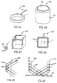
- Figs. 4a and 4b illustrate one possible design for the illumination assembly 40 .
- the illumination assembly 40 is composed of a corresponding number of light sources, each associated with a corresponding one of the optical assemblies (not shown here).
- a light source is designed like a ring 41 formed by a plurality of LEDs or optical fibers (not shown).
- an external light source (not shown) associated with a fiber bundle 42 may be used.
- the ring 41 would enclose the corresponding field lens (not shown).
- the light source is designed like a cylinder 43 , which also may be formed by a plurality of LEDs.
- the illumination assembly 40 may include either a single elongated light source mounted in the proximity of the field lenses 34 of the optical assemblies so as to extend along the Y -axis, or a pair of such elongated light sources mounted at opposite sides of the optical assemblies.
- Figs. 4c-4f there is illustrated another possible design of a dark-field illumination assembly 140 , aimed at providing the illumination of each region on the wafer at substantially 45°-angle between the vertical plane defined by the average direction of the incident beam propagation and those of the pattern (as seen from the top).
- a pattern on the wafer is typically arranged in the so-called “streets-and-avenues” manner, and the illumination at 45°-azimuth angle, ⁇ , enables to eliminate or at least significantly reduce the undesirable diffraction effects caused by the pattern.
- the illumination assembly 140 is in the form of a corresponding number of light sources, each in the form of a rectangular frame carrying a plurality of light emitting elements 142 (e.g., LEDs) and a plurality of identical transparent ball-like lenses 144 for directing emitting light towards the inspection plane.
- the lens 144 may be of another suitable shape, being shaped like a ball in the present example.
- the balls 144 are arranged in rows and columns so as to form four sides of the rectangular frame, such that contact is provided between each two adjacent balls.
- Each of the light emitting elements is located in the corresponding one of the spaces formed between the balls.
- the ball 144 has the diameter of about 3mm, and is made either from glass or optical-quality plastic.
- the light source 142 is about 0.3mm in size.
- the projection of a field of view F i of the corresponding sensor AS 1 is located in the center of the horizontal plane defined by the rectangular frame 140 enclosing the field of view F i .
- the length of the frame's wall is about 1.5-2 times larger than that of the field of view F i of the area sensor.
- Figs. 4e and 4f partly show top and side views, respectively, of the balls-LEDs assembly 140 .
- Each ball 144 serves as a lens accommodated in the optical path of a light beam B emitted by the corresponding LED 142 .
- the light beams B propagate through the corresponding balls 144 and, whilst ensuing therefrom, become directed onto the wafer W at 45°-azimuth angle.
- the emitting surface of the LED is appropriately oriented with respect to the corresponding balls, and is located in the focus plane thereof.
- the 45°-angle provided by the LED-balls assembly is the azimuth angle, while an elevation angle, ⁇ , may be different.
- Eletitude angle used herein is the angle between the incident beam and the wafer's plane as seen from the side.
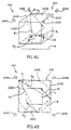
- a dark-field illumination assembly generally designated 240 , aimed at providing the illumination with the substantially 45°-angle.
- the illumination assembly 240 comprises a plurality of light sources each in the form of a rectangular frame 242 carrying four light emitting elements (e.g., LEDs) 244a , 244b , 244c and 244d which are accommodated at the upper corners of the frame 242 , respectively, aimed at providing the propagation of their central beams at the opposite corners.
- the inner surfaces 242a-242d of the frame 242 are mirrors.
- the frame 242 is vertically aligned with the corresponding field lens 34 .
- the construction is such that the projection of the field of view F of the corresponding sensor (not shown) occupies the central region of the frame.
- the light emitting elements 244a-244d are accommodated in the focal plane of the field lens 34 .
- Each light emitting element emits a beam B , which slightly diverges, e.g., within the angle of 14°, and, while propagating towards the lens 34 through the frame 242 , is sequentially reflected from two adjacent mirrors located opposite (along the diagonal axis) to the corresponding light emitting element.
- light beams emitted by all the emitting elements end propagating as described above impinge onto the field lens 34 at the substantially near 45°-angle, which lens produces collimated beams of 45°-azimuth angle of incidence.
- This construction provides the dark-field illumination of an area within the entire field of view F of the area sensor, with the desired uniformity of illumination.
- the illumination assembly operating in the dark-filed illumination mode is optional. Should this assembly be used, its operation is timely separated from the operation of the bright-field illumination assembly 24 , and it may be operated selectively. In other words, whilst continuously inspecting the wafer using the illumination assembly 24 , at selective locations on the wafer (strips), the operation of the assembly 24 is halted and the dark-field illumination assembly is switched-on. These selective locations may be those, where a potential defect has been detected during the bright-field illumination mode of the system 12 , or a real defect is expected, which is usually the case when dealing with such patterned workpieces as wafers.
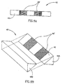
- a scanning technique suitable to be used in the present invention aimed at inspecting a strip-like scanning field SF on the wafer by all the sensors AS 1 -AS 5 .
- the fields of view F 1 -F 5 of the sensors AS 1 -AS 5 are aligned along the Y -axis and define together a continuous scanning field SF that extends along the wafer's diameter.
- the movement of the housing 22 along the X -axis is such so as to provide a small overlap region 44 between the scanning fields of each two locally adjacent positions of the sensors AS 1 -AS 5 .
- the entire scanning field is formed by the fields of view F 1 -F 5 of all the sensors AS 1 -AS 5 .
- These fields of view cover a corresponding number (five in the present example) spaced-apart areas aligned along the Y -axis, rather than the overlapping areas as in the previously described example
- a scanning field is "discontinuous". This is associated with the fact that the specular reflection from a patterned article, such as wafer, will unavoidably require the field lens to be at least slightly larger than the field of view of the area sensor, which creates the spaces between the fields of views of the adjacent sensors.
- Fig. 5a When dealing with the detection of non-specular reflected light (Lambertian), the example of Fig. 5a provides sufficient results.
- additional step-like movement of the optics (and, optionally, the corresponding sensors) is provided along the Y -axis, with a pitch not less than the space between the areas (preferably, slightly exceeding this space).
- a so-called “calibration target” is formed along a strip 23 on the window 22a .
- the calibration target 23 serves for calibrating the sensors prior to inspection, for example, correcting the non-uniformity of illumination, etc.
- FIG. 6 illustrating an optical inspection system 112 constructed according to another embodiment of the invention, suitable to be used in the photolithography tools arrangement of either of Figs. 2a or 2b.
- the same reference numbers are used for identifying common components of the systems 12 and 112 , and the beam propagation is shown schematically.
- a scanning apparatus 116 of the system 112 has a somewhat different construction as compared to that of the system 12 .
- the following elements are accommodated inside the housing 22 : optical assemblies OA 1 -OA 5 , illumination assembly 40 , sensors AS 1 -AS 5 , a plurality of mirrors 46 (or a single elongated mirror) aligned along the Y -axis above the optical assemblies, imaging tube lenses 38 and an additional light directing assembly 48 .
- the drive mechanism D 2 is also mounted inside the housing 22 and is coupled to the optical assemblies OA 1 -OA 5 and to the mirror(s) 46 for driving the reciprocation movement thereof.
- the sensors AS 1 -AS 5 are stationary mounted inside the housing 22 , rather than being mounted for movement together with the optical assemblies OA 1 -OA 5 .
- the additional light directing assembly 48 serves for dividing the returned light components B i ' reflected from the mirror 46 into two groups 49a and 49b propagating, respectively, along the Z - and X -axes.
- the sensors AS 1 -AS 5 are aligned in two parallel lines L 1 and L 2 which extend along the Y -axis and are spaced from each along the X -and Z -axes. Each two adjacent sensors are spaced from each other along the X -and Z -axes.
- the light directing assembly 48 is in the form of a parallelepiped, which is substantially optically transparent, except for spaced-apart reflective regions 49b formed on its inner diagonal surface 49 .
- the light directing assembly 48 may be constructed by attaching a pair of parallel sides of a pair of symmetrically identical triangular prisms 48a and 48b to each other. One of these parallel sides has the patterned surface 49 .
- the pattern may, for example, be made by depositing a reflective material onto the regions 49a through a mask. It should be noted, although not specifically shown, that beam-splitter cubes may replace the prisms 48a and 48b .
- the operation of the system 112 is generally similar to that of the system 12 .
- the moving elements i.e., the optical elements OA 1 -OA 5 , mirror(s) 46 , and, optionally, the illumination assembly 40 ) step-by-step move along the X -axis between the center region and the periphery region of the wafer (i.e., within the inspection area IA ).
- One half of the wafer is strip-by-strip inspected.
- the stage 16 rotates by 180° parallel to the inspection plane IP , resulting in that the other half of the wafer is positioned within the inspection area IA , and the inspection is repeated by step-by-step moving the respective elements from the periphery region of the wafer towards its center region.
- the moving elements may be returned to their initial position above the center region of the wafer prior to starting the inspection of the second half of the wafer.
- the inspection proceeds from the center region to the periphery region of the wafer.
- Fig. 5b it should be understood that various operational modes are possible. For example, after completing the scanning of the half of the wafer by step-by-step movements along the X -axis, the fields of view of the sensors are shifted along the Y -axis and the inspection area IA is passed with this shifted position of the fields of view. In this case, the sensors may and may not be returned into their initial position relative to the wafer prior to the shifting procedure.
- An alternative operational mode consists of step-by-step performing the Y -axis shift of the fields of view for each sensors' position along the X -axis.
- the number of area sensors, and, accordingly, of the optical assemblies, suitable to be used in the system 12 , 112 is dictated by the dimensions of the wafer to be inspected and the desired image resolution. For example, if a standard 200mm wafer should be inspected with the resolution of 50 ⁇ m, eight commercially available TV cameras (i.e., each having approximately 500x600 pixels) may be used as the area sensors.
- the scanning time at each relative location of the moving components relative to the wafer is approximately 170msec
- the time for moving these elements from strip to strip is about 0.5sec
- the inspection area one half of the wafer
- the total inspection time for the entire wafer is about 5.4sec.
- total inspection time per wafer would be about 10sec. It is understood that such brief inspection time would not affect the throughput of the photolithography tools arrangement, nor would it impede the regular operation of the robot.
- a large area of the wafer i.e., a strip extending along the entire diameter of the wafer
- the illumination assembly may comprise a suitable number of light sources.
- a single light source equipped with suitable light splitting means capable of producing a plurality of incident light components may be provided.
- Figs. 9a and 9b illustrate two possible constructions of such an illumination assembly having a single light source.
- an illumination assembly 124 comprises a lamp 50 associated with a plurality of condensers C 1 - C 8 and optical fibers OF 1 -OF 8 (constituting a light guiding means), eight in the present example, considering eight cameras and eight optical assemblies.
- Eight shutters, generally at 52 are provided, each associated with a corresponding one of the optical fibers.
- the shutters may be of either mechanical or electrooptical type.
- the provision of the shutters 52 is aimed at the following. Whilst illuminating the plurality of regions within the illuminated strip S through separate field lenses 34 , a certain overlap of two locally adjacent illuminated regions occurs, unavoidably resulting in the non-uniform illumination within such an overlapping area. To avoid this effect, the array of the regions within the strip S may be illuminated sequentially, by sequentially opening the shutters 52 . Alternatively, the shutters may be operated in such a manner that the regions illuminated at each time unit are disposed in a so-called "chess-board" order, thereby enabling the interlaced illumination. It should be noted that such shutters enabling the sequential illumination of the array of regions within the strip or the interlaced illumination of these regions may also be used with a plurality of separate light sources.
- Fig. 9b illustrates a section view of an illumination assembly 224 having a somewhat different construction as compared to the assembly 124 .
- the assembly 224 similarly to the assembly 124 , includes the lamp 50 , a condenser 51 and a plurality of optical fibers (fibers OF 1 and OF 5 are shown in the figure), but is also provided with a mirror 54 .
- the mirror 54 is mounted in the optical path of a primary beam B , and is rotatable, preferably step-by-step, about an axis AP of propagation of the beam B towards the mirror 54 , by a suitable driver (not shown).
- the mirror 54 is oriented at 45° to the vertical axis AP , and rotates in the horizontal plane, the input faces of the optical fibers being arranged in a spaced-apart relationship in the horizontal plane.
- the rotation of the mirror 54 will result in the sequential illumination of the input faces of the optical fibers and, consequently, the regions within the strip S .
- the frequency of the rotation of the mirror 54 is about 7Hz.
- Fig. 10 partly illustrates the scanning apparatus 18 .
- the wafer W under inspection is located in a focal plane FP of the objective lens assemblies (shown here as field lenses 34 ).
- the calibration pattern 23 is provided serving for calibrating the sensors prior to inspection, and should therefore be also located in the focal plane FP .
- the calibration pattern 23 extends parallel to the inspection plane IP but is located in a plane IP' perpendicular thereto, and a mirror 56 is accommodated in the optical path of the incident beam ensuing from the field lens 34 .
- the location of the mirror is selected such as to ensure that the optical distance d 1 between the optical window 22A and the wafer (i.e., the focal plane FP ) is equal to the distance d 2 between the plane IP' and a point 56A of incidence of the beam B 1 onto the mirror 56 .
- the mirror 56 is mounted stationary, and therefore does not impede the inspection of the half of the wafer through the moving optical assemblies.
- a glass-piece 58 is preferably accommodated in the optical path of the incident beam B 1 on its way towards the calibration pattern 23 . This enables to obtain substantially identical conditions for light propagation during the inspection and calibration procedures.
- the advantages of the present invention are self-evident.
- the optical inspection system constructed and operated according to the invention is compact, provides for maintaining the wafer stationary during the inspection and utilizes a rigid and very stable scanning apparatus capable of fast scanning of the wafer.
- the scanning apparatus is fully separated from the photolithography environment owing to the fact that all moving components of the scanning apparatus are located within the sealed housing 22 , while the control unit 26 and illumination assembly 24 are located outside the track clean area.
- the optical inspection system according to the invention has the option to be bypassed by the production process and to be simultaneously operated in off-line or integrated modes.
Abstract
Description
- The present invention is in the field of automatic inspection techniques, and relates to an optical inspection method and system, particularly useful for inspecting semiconductor wafers progressing on a production line.
- The manufacture of semiconductor devices consists of a multi-staged process requiring wafers progressing on a production line to be inspected between sequential manufacturing steps. One of the principle processes in the manufacture of semiconductor devices is the photolithography process. It consists of patterning the wafer's surface in accordance with the active elements of semiconductor devices to be manufactured. The photolithography process includes the following main operational steps:
- a. Coating the wafer with a photoresist material;
- b. Exposing the photoresist material through a mask with a predetermined pattern in order to produce a latent image of the mask on the photoresist material; and
- c. Developing the exposed photoresist material in order to produce the image of the mask on the wafer.
-
- Generally speaking, prior to the photolithography process, the wafer is prepared for the deposition of one or more layers. After the completion of the photolithography process, the uppermost layer of the wafer is etched. Then a new layer is deposited, in order to start the photolithography and etching operations again. In this repetitive manner, a multi-layer semiconductor wafer is produced.
- Fig. 1 illustrates a block diagram of a
typical photocluster 1 used for performing the photolithography process in semiconductor fabrication plants (FABs). The photocluster 1 (or link) is composed of two main parts: aphototrack 2 and an exposure tool 4. Thephototrack 2 includes acoater track 6 associated with a cassette load station 6a, and adeveloper track 8 associated with a cassette unload station 8a. Alternatively, both coating and developing functions may be combined and realized in a common station. A load/unload robot R is mounted for movement within thephotocluster 1 for conveying wafers W to and from the photocluster tools. Thecoater track 6, the exposure tool 4 and thedevelopment track 8 are tightly joined together in order to minimize process variability and any potential risk of contamination during photolithography, which is a super sensitive process. - It is apparent that in such a complex and delicate production process various problems, failures or defects may arise or develop during each manufacturing step or from the serial combination of steps. Due to the stringent quality requirements, any defect which is not timely detected, may result in the rejection of a single wafer or the entire lot. The wafer cannot be taken out of the photocluster tools set-up for measurement or inspection before the entire photolithography process is completed and the wafer arrives at the cassette station 8a. The wafers are typically inspected at a stand-alone monitoring system (CD-SEM) which is installed outside the production line, and to which the wafers are transferred by means of a separate handling system. This reduces the throughput of the production line.
- A manual inspection technique is conventionally used for inspecting the wafers for so-called macro lithography defects, such as scratches or foreign particles of dust and dirt. Generally, macro defects are considered as defects having tenths of micrometers in size. The manual inspection technique utilizes the visual examination of the wafer's surface by an operator using intense light and magnification. This inspection is inconsistent and unreliable, since the results vary significantly amongst operators, due to the wafer's complexity and depending on the operators' experience. About 80% of the photo-related defects remain undetected. Manual inspection has low throughput, and could not be performed within the FAB tools. Manual inspection is not cost effective.
- Various automatic inspection systems have been developed. They utilize either a line CCD camera or an area CCD camera. The basic problem with line type detectors is their non-effective use of illuminating radiation. This is owing to the fact that a strip illuminated on the surface of the wafer under inspection is substantially wider than the width of the field of view of a line CCD camera. Additionally, the line CCD based technique suffers from a complicated mechanical arrangement needed for moving the line CCD camera along the X- and Y- axes relative to the wafer under inspection. Moreover, different resolutions are achieved in the X- and Y- directions, due to the movement of the image during scanning.
- As for the area sensor based technique, it utilizes a so-called step-and-repeat mode of operation, wherein the camera and the wafer are mounted for movement relative to each other to cover the entire surface of the wafer. More specifically, the camera and the wafer are moved step-by-step, and images are acquired upon the camera or the wafer stops. This technique requires a quite complicated mechanical stage providing movement along two mutually perpendicular axes. Additionally, it results in low throughput due to a great number of movement steps, and requires an additional footprint for performing such a two-dimensional movement.
- Machine vision systems having multiple cameras have been developed, being disclosed, for example, in U.S. Patent No. 5,768,443. In this system, images are acquired simultaneously by a plurality of cameras. The fields of view of the cameras cover a relatively large area of the wafer under inspection, thereby increasing the throughput of the system, as compared to the techniques utilizing a single line or area sensor. However, this patent does not present any example of the cameras' arrangement, which would be useful in an integrated inspection. An inspection machine should be inexpensive, simple to erect and maintain, and should have a small footprint (like a wafer cassette) to meet the requirements of the integrated inspection.
- Laser inspection systems have been developed which utilize various types of scanners and collectors for scanning the wafer's surface during the translational movement and for collecting light reflective and scattered from the surface. Such systems are disclosed, for example, in U.S. Patent Nos. 4,630,276; 5,108,176; 5,127,726 and 5,712,701. Unfortunately, these systems are complicated and expensive. Since they use monochromatic laser illumination, they are non-effective and insufficient for the inspection of developed photoresist for macro defects.
- There is accordingly a need to facilitate the automatic inspection of workpieces progressing on a production line, by providing a novel system and method for the optical inspection of such workpieces.
- It is a major feature of the invention that the optical inspection system may be integrated into the production line. It is simple, inexpensive and compact, and provides for inspection with a high throughput of workpieces.
- The main idea of the present invention is based on the following. A semiconductor wafer is typically a substantially flat workpiece, having an axis of symmetry (i.e. is round). Consequentially, one half of the wafer can be inspected by appropriately moving respective parts of a scanning apparatus above it, and, upon rotating the wafer about its axis of symmetry by 180°, inspecting the other half of the wafer. Hence, suitable mechanics should be provided for moving the respective components of the scanning apparatus solely within an inspection area equal to the half of the wafer, rather than moving them above the entire wafer, or moving both the respective components and the wafer relative to each other. This significantly simplifies the mechanical equipment of the entire system, as well as its footprint, and enables the use of a robot typically installed in the production line for conveying wafers to and from a plurality of stations. To scan the half of the wafer (inspection area), a plurality of optical assemblies is mounted for movement above the wafer within the inspection area, the optical assemblies being aligned in a line parallel to the axis of symmetry of the wafer between the opposite sides thereof. A plurality of sensors is provided, each sensor being associated with a corresponding one of the plurality of optical assemblies. Thus, an illuminated strip extending along the entire width of the wafer is inspected at each location of the plurality of optical assemblies relative to the wafer.
- There is thus provided, according to one aspect of the present invention, an optical inspection system for detecting defects on a substantially flat workpiece having an axis of symmetry, the system comprising a stage supporting said workpiece in an inspection plane, and a scanning apparatus accommodated above said workpiece, wherein:
- (a) said stage is mounted for rotation in a plane parallel to said inspection plane;
- (b) said scanning apparatus comprises:
- an illumination assembly producing a plurality of incident radiation components, each component illuminating a corresponding one of a plurality of regions of the workpiece within a strip illuminated by said plurality of incident radiation components, the strip extending parallel to the axis of symmetry of the workpiece between two opposite sides thereof;
- a plurality of optical assemblies accommodated above said workpiece, each optical assembly directing a corresponding one of a plurality of radiation components returned from the corresponding illuminated region away from the workpiece, wherein the optical assemblies are aligned along said axis of symmetry in a spaced-apart parallel relationship and mounted for reciprocating movement within a plane parallel to an inspection area, said inspection area covering substantially a half of the workpiece;
- (c) a plurality of area sensors are arranged in a predetermined manner, each area sensor being associated with a corresponding one of the optical assemblies for receiving the component of the returned radiation and generating data representative thereof;
- (d) a first drive mechanism is coupled to said optical assemblies for driving said reciprocating movement thereof; and
- (e) a second drive mechanism is coupled to said stage for driving said rotation thereof.
-
- The illumination assembly may operate in bright-field illumination mode. In this case, it comprises a plurality of stationary mounted light sources aligned corresponding to the alignment of the optical assemblies, each incident radiation component being directed on the corresponding optical assembly, which, in turn, directs it onto the corresponding region of the workpiece.
- Alternatively, or additionally, the illumination assembly may operate in a dark-filed illumination mode. In this case, it includes either a plurality of light sources, each accommodated in the vicinity of the corresponding optical assembly, or an elongated light source, extending along the optical assemblies in the proximity thereof. This "dark-field" illumination assembly is mounted for movement together with the optical assemblies. If the dark-field light illumination is used in addition to the bright-field illumination, the operation of the stationary mounted light sources and the operation of the movable light sources are time separated. For example, the stationary mounted light sources may be continuously operated, while the movable light sources are selectively actuated to inspect only those locations on the workpiece where either a potential defect has been detected during the bright-field mode, or a real defect is expected.
- The area sensors may be arranged in a line parallel to the axis of symmetry and associated with the optical assemblies, so as to move together with the optical assemblies. Alternatively, the area sensors may be arranged in two parallel lines, parallel to the axis of symmetry, wherein each two adjacent sensors are displaced from each other along two mutually perpendicular axes. In this case, an additional light directing assembly is provided for receiving the components of the returned radiation ensuing from the optical assemblies, and directing them onto to the area sensors.
- According to another aspect of the present invention, there is provided a photolithography tools arrangement for processing a stream of substantial flat workpieces progressing on a production line, which tools arrangement comprises an optical inspection system constructed as described above.
- According to yet another aspect of the present invention, there is provided a method for inspecting a substantial flat workpiece having an axis of symmetry, the method comprising the steps of:
- (i) locating the workpiece within an inspection plane;
- (j) illuminating a plurality of regions of the workpiece by a plurality of incident radiation components and producing a plurality of light components returned from the plurality of illuminated regions, the illuminated regions forming an illuminated strip extending parallel to the axis of symmetry between two opposite sides of the workpiece;
- (k) directing each of the plurality of light components returned from the illuminated regions through a plurality of optical assemblies aligned in a line parallel to the axis of symmetry above the workpiece;
- (l) detecting light components returned from the illuminated regions by a corresponding plurality of area sensors;
- (m) moving said plurality of optical assemblies relative to said workpiece within a plane parallel to the inspection plane, such as to illuminate successive strips on the workpiece and detect light components returned therefrom;
- (n) repeating steps (j) to (m) for strip-by-strip inspection of the workpiece within an inspection area that covers substantially a half of the workpiece;
- (o) rotating said workpiece by 180° and repeating steps (j) to (n).
-
- More specifically, the present invention is used for inspecting wafers progressing within a photolithography tools set-up, and is therefore described below with respect to this application.
- In order to understand the invention and to see how it may be carried out in practice, a preferred embodiment will now be described, by way of non-limiting example only, with reference to the accompanying drawings, in which:
- Fig. 1 schematically illustrates a block diagram of the main components of the conventional photocluster;
- Figs. 2a and 2b schematically illustrate by way of a block diagram two different examples, respectively, of a photolithography arrangement including an optical inspection system according to the present invention;
- Figs. 3a and 3b schematically illustrate the main components of the optical inspection system of either of Figs. 2a or 2b, constructed according to one embodiment of the invention;
- Figs. 4a and 4b illustrate two possible examples of implementation of an illumination assembly of the system of Fig. 3 operating in a dark-field illumination mode;
- Figs. 4c to 4f illustrate another possible example of a dark-field illumination assembly;
- Figs. 4g and 4h illustrate yet another possible example of a dark-field illumination assembly;
- Figs. 5a and 5b illustrated two different examples, respectively, of a scanning technique suitable to be used in the present invention;
- Fig. 6 schematically illustrates the main components of the optical inspection system of either of Figs. 2 or 3, constructed according to another embodiment of the invention;
- Fig. 7 more specifically illustrates an arrangement of sensors of the system of Fig. 6;
- Figs. 8a and 8b more specifically illustrate a light directing assembly of the system of Fig. 6;
- Figs. 9a and 9b illustrate two different examples, respectively, of the illumination assembly suitable for use in the system of either of Figs. 3a-3b or 6; and
- Fig. 10 illustrates more specifically some features of the scanning apparatus of Figs. 3a-3b.
-
- Fig. 1 illustrates the configuration of the
conventional photocluster 1, which comprises thephototrack 2 and the exposure tool 4, wherein the photo track is composed of thewater track 6 and thedeveloper track 8. The water and developer tracks have their associated cassette load and unload stations 6a and 8a, respectively. The cassettes containing wafers are supplied to thephototrack 2, being loaded from the station 6a onto thecoater track 6. Here, a photoresist material is deposited onto the wafer's surface, and then the robot R transmits the coated wafer to the exposure tool 4. The photoresist coating is exposed to light through a mask having a predetermined pattern to produce a latent image of the mask on the photoresist coating. Thereafter, the robot R transmits the wafer to thedeveloper track 8 for developing the latent image. - Referring to Fig. 2a, there is illustrated a photocluster 10 (constituting a photolithography tools arrangement) constructed according to one example of the invention. The same reference numbers are used for identifying those components which are common in the
photoclusters photocluster 10 is constructed generally similar to theconventional photocluster 1, but comprises anoptical inspection system 12, constructed and operated according to the invention, as will be described further below. Theoptical inspection system 12 is compact so as to be easily installed within the conventionally designed photocluster, enabling the use of the same robot R for feeding and discharging the wafers to and from theinspection system 12. Thesystem 12 may be dimensioned and shaped similar to that of the conventional cassette. Generally, the exact location of theinspection system 12 within the photocluster is selected in accordance with the considerations and circumstances of a specific manufacturer, an available foot-print inside the phototrack and the FAB considerations. Since theinspection system 12 is extremely compact, it can be positioned at a cassette location in the unloading area, or any other location accessible for the load/unload robot R. - Fig. 2b illustrates a
photolithography tools arrangement 14, constructed according to another example of the invention. Thearrangement 14 utilizes thephotocluster 1 and theoptical inspection system 12, which is installed as a stand-alone unit within thephotolithography tools arrangement 14 similar to the wafers' load/unloadcassette station 15. The robot R conveys wafers from thecassette 15 to theinspection system 12 and returns the inspected wafers back to thecassette station 15, and supplies and discharges wafers to and from thephotocluster 1. - Fig. 3a illustrates the main constructional parts of the
optical inspection system 12, constructed according to one embodiment of the invention. Theinspection system 12 comprises ascanning apparatus 16 for inspecting a wafer W located on asupport stage 18, which supports the wafer W in an inspection plane IP. The wafer W has an axis of its symmetry OP defining half-parts P1 and P2 of the wafer W at opposite sides of the axis OP. Coupled to thestage 18 is a first drive mechanism D1 for driving the rotational movement of thestage 18 within a plane parallel to the inspection plane IP. - The
scanning apparatus 16 inspects the wafer W within an inspection area IA defined by the half P1 of the wafer, as will be described more specifically further below. Then, the drive mechanism D1 operates to rotate thestage 18 by 180°, thereby locating the other half P2 of the wafer within the inspection area IA. - The
scanning apparatus 16 comprises a sealedhousing 22 containing a plurality of optical assemblies, for example five optical assemblies OA1-OA5 , and a corresponding plurality of area sensors AS1-AS5 . Anillumination assembly 24 and acontrol unit 26 are accommodated outside thehousing 22. Thehousing 22 is formed with an optically transparent bottom portion 22a (i.e., window) substantially covering the inspection area IA (one half of the wafer). A second drive mechanism D2 is accommodated inside the housing so as to be outside the inspection area IA. The drive mechanism D2 is associated with the optical assemblies OA1-OA5 and with the area sensors AS1-AS5 for driving a reciprocation movement thereof along the X-axis within the inspection area IA. It is understood, although not specifically shown, that a suitable guiding assembly is provided for slidingly supporting the moving parts (i.e., optical assemblies and area sensors) inside thehousing 22. - The optical assemblies OA1-OA5 are accommodated above the window 22a being aligned along the Y-axis parallel to the axis of symmetry OP in a spaced-apart parallel relationship between the opposite sides of the wafer. The sensors AS1-AS5 are arranged like a "rule" extending along the Y-axis and spaced from the optical assemblies along the Z-axis.
- The construction and operation of the
control unit 26 do not form part of the present invention and may be of any known suitable kind, and therefore need not be specifically described, except to note the following. Thecontrol unit 26 includes several suitable utilities. Some of them are associated with the sensors AS1-AS5 for receiving and analyzing data representative of radiation returned from the wafer W, and the other are associated with the driver assemblies D1 and D2 for synchronizing the movements of thestage 16 and moving components of the scanning apparatus. Thecontrol unit 26 is typically a computer device comprising a suitable pattern recognition software and a translation means so as to be responsive to data representative of the radiation returned from the wafer W and locate defects, if any. This software generates a gray level bit map of the acquired images, which may, for example, be stored in a memory. Generally speaking, the analyzing of the obtained data is performed in a die-to-die, die-to-many dies or die-to-database manner. Thecontrol unit 26 and theillumination assembly 24 are located outside the area occupied by thephotocluster 1. - It should be noted that to facilitate the image processing, pre-alignment of the wafer W could be provided. When the wafer W is set on to the
stage 18, thecontrol unit 26 may operate the driver assemble D1 to rotate the wafer W, and operate the periphery sensors, e.g. AS1 and AS5 , along with the corresponding illuminating assemblies, to acquire images of the wafer's edge and analyze them, so as to detect a registration mark, i.e., "notch" or "flat". After the notch or flat is detected, the wafer could be turned so as to provide desired orientation of the main wafer direction. Preferably, the main wafer direction coincides with the X-axis, i.e., with the direction of movement of the optical assemblies OA1-OA5 . - Fig. 3b schematically illustrates the main operational principles of the
system 12. The beam propagation is shown here schematically to facilitate the illustration. Theillumination assembly 24 comprises a suitable number of light sources or a single light source equipped with suitable light splitting means, capable of producing a plurality of incident light components. A corresponding number oflenses 30 are stationary mounted inside thehousing 22 being aligned according to that of the optical assemblies. Each incident light component impinges onto a corresponding one of the optical assemblies (five in the present example), the component B1 associated with the optical assembly OA1 being seen in Fig. 3b. The optical assembly OA1 comprises abeam splitter 32 and an objective lens assembly including inter alia afield lens 34. The area sensor AS1 is associated with animaging tube lens 38. - The
beam splitter 32 directs the incident light component B1 onto the objective lens assembly (only thefield lens 34 thereof being shown here), which, in turn, focuses the light component B1 onto a region S1 on the wafer. A light component B1' returned from the illuminated region S1 is directed onto thelens 38 by thebeam splitter 32. It is understood, although not specifically shown, that regions illuminated by all the incident light components via the optical assemblies OA1-OA5 form together the illuminated strip S extending parallel to the diameter of the wafer W. Hence, whilst step-by-step moving the optical assemblies and area sensors from the center region of the wafer towards its periphery region along the X-axis, the half of the wafer located within the inspection area IA is strip-by-strip inspected. At each relative location of the moving elements relative to the wafer, each of the sensors AS1-AS5 acquires an image of the illuminated region S1 and generates data representative thereof. The respective utilities of thecontrol unit 26 receive and analyze these data to locate defects, if any, within the entire illuminated strip S composed of the regions S1-S5 . - The
illumination assembly 24 operates in a so-called "bright-field illumination" mode. As further shown in Fig. 3b, thescanning apparatus 18 comprises anadditional illumination assembly 40 mounted inside thehousing 22 for the purpose to move together with the optical assemblies OA1-OA5 and sensors AS1-AS5 within the inspection area IA. - Figs. 4a and 4b illustrate one possible design for the
illumination assembly 40. In both examples, theillumination assembly 40 is composed of a corresponding number of light sources, each associated with a corresponding one of the optical assemblies (not shown here). According to the example of Fig. 4a, such a light source is designed like aring 41 formed by a plurality of LEDs or optical fibers (not shown). In the case of optical fibers, an external light source (not shown) associated with afiber bundle 42 may be used. Thering 41 would enclose the corresponding field lens (not shown). In the example of Fig. 4b, the light source is designed like acylinder 43, which also may be formed by a plurality of LEDs. It should, however, be noted that theillumination assembly 40 may include either a single elongated light source mounted in the proximity of thefield lenses 34 of the optical assemblies so as to extend along the Y-axis, or a pair of such elongated light sources mounted at opposite sides of the optical assemblies. - Turning now to Figs. 4c-4f, there is illustrated another possible design of a dark-
field illumination assembly 140, aimed at providing the illumination of each region on the wafer at substantially 45°-angle between the vertical plane defined by the average direction of the incident beam propagation and those of the pattern (as seen from the top). This is associated with the fact that a pattern on the wafer is typically arranged in the so-called "streets-and-avenues" manner, and the illumination at 45°-azimuth angle, α, enables to eliminate or at least significantly reduce the undesirable diffraction effects caused by the pattern. - As shown in Fig. 4c, the
illumination assembly 140 is in the form of a corresponding number of light sources, each in the form of a rectangular frame carrying a plurality of light emitting elements 142 (e.g., LEDs) and a plurality of identical transparent ball-like lenses 144 for directing emitting light towards the inspection plane. It should, however, be noted that generally thelens 144 may be of another suitable shape, being shaped like a ball in the present example. Theballs 144 are arranged in rows and columns so as to form four sides of the rectangular frame, such that contact is provided between each two adjacent balls. Each of the light emitting elements is located in the corresponding one of the spaces formed between the balls. Theball 144 has the diameter of about 3mm, and is made either from glass or optical-quality plastic. Thelight source 142 is about 0.3mm in size. - As shown in Fig. 4d, the projection of a field of view Fi of the corresponding sensor AS1 is located in the center of the horizontal plane defined by the
rectangular frame 140 enclosing the field of view Fi . The length of the frame's wall is about 1.5-2 times larger than that of the field of view Fi of the area sensor. - Figs. 4e and 4f partly show top and side views, respectively, of the balls-
LEDs assembly 140. Eachball 144 serves as a lens accommodated in the optical path of a light beam B emitted by the correspondingLED 142. The light beams B propagate through the correspondingballs 144 and, whilst ensuing therefrom, become directed onto the wafer W at 45°-azimuth angle. To this end, the emitting surface of the LED is appropriately oriented with respect to the corresponding balls, and is located in the focus plane thereof. It should be noted that the 45°-angle provided by the LED-balls assembly is the azimuth angle, while an elevation angle, , may be different. The term "elevation angle" used herein is the angle between the incident beam and the wafer's plane as seen from the side. - Referring to Figs. 4g and 4h, there is illustrated yet another possible design of a dark-field illumination assembly, generally designated 240, aimed at providing the illumination with the substantially 45°-angle. This example presents a so-called "retro-reflective scheme". The
illumination assembly 240 comprises a plurality of light sources each in the form of arectangular frame 242 carrying four light emitting elements (e.g., LEDs) 244a, 244b, 244c and 244d which are accommodated at the upper corners of theframe 242, respectively, aimed at providing the propagation of their central beams at the opposite corners. The inner surfaces 242a-242d of theframe 242 are mirrors. Theframe 242 is vertically aligned with thecorresponding field lens 34. The construction is such that the projection of the field of view F of the corresponding sensor (not shown) occupies the central region of the frame. The light emitting elements 244a-244d are accommodated in the focal plane of thefield lens 34. Each light emitting element emits a beam B, which slightly diverges, e.g., within the angle of 14°, and, while propagating towards thelens 34 through theframe 242, is sequentially reflected from two adjacent mirrors located opposite (along the diagonal axis) to the corresponding light emitting element. - As better shown in Fig. 4h, the opposite, periphery light components B1 and B2 of the diverging beam B (solid angle) emitted by the light emitting element 244a impinge onto the mirrors 242c and 242d, and being reflected therefrom, fall onto the mirrors 242d and 242c, respectively, which, in turn, reflect the light components B2 and B1 towards the
lens 34. As a result light beams emitted by all the emitting elements end propagating as described above impinge onto thefield lens 34 at the substantially near 45°-angle, which lens produces collimated beams of 45°-azimuth angle of incidence. This construction provides the dark-field illumination of an area within the entire field of view F of the area sensor, with the desired uniformity of illumination. - It should be noted that the provision of the illumination assembly operating in the dark-filed illumination mode is optional. Should this assembly be used, its operation is timely separated from the operation of the bright-
field illumination assembly 24, and it may be operated selectively. In other words, whilst continuously inspecting the wafer using theillumination assembly 24, at selective locations on the wafer (strips), the operation of theassembly 24 is halted and the dark-field illumination assembly is switched-on. These selective locations may be those, where a potential defect has been detected during the bright-field illumination mode of thesystem 12, or a real defect is expected, which is usually the case when dealing with such patterned workpieces as wafers. - Referring to Figs. 5a and 5b, there are illustrated two different examples of a scanning technique suitable to be used in the present invention, aimed at inspecting a strip-like scanning field SF on the wafer by all the sensors AS1-AS5 . As shown in Fig. 5a, the fields of view F1-F5 of the sensors AS1-AS5 are aligned along the Y-axis and define together a continuous scanning field SF that extends along the wafer's diameter. The movement of the
housing 22 along the X-axis is such so as to provide asmall overlap region 44 between the scanning fields of each two locally adjacent positions of the sensors AS1-AS5 . - In the example of Fig. 5b, at each current position of the sensors AS1-AS5 along the X-axis, the entire scanning field is formed by the fields of view F1-F5 of all the sensors AS1-AS5 . These fields of view cover a corresponding number (five in the present example) spaced-apart areas aligned along the Y-axis, rather than the overlapping areas as in the previously described example In other words, such a scanning field is "discontinuous". This is associated with the fact that the specular reflection from a patterned article, such as wafer, will unavoidably require the field lens to be at least slightly larger than the field of view of the area sensor, which creates the spaces between the fields of views of the adjacent sensors. When dealing with the detection of non-specular reflected light (Lambertian), the example of Fig. 5a provides sufficient results. To cover the spaces between the locally adjacent areas, thereby providing the continuous scanning field SF, additional step-like movement of the optics (and, optionally, the corresponding sensors) is provided along the Y-axis, with a pitch not less than the space between the areas (preferably, slightly exceeding this space).
- Turning back to Fig. 3a, a so-called "calibration target" is formed along a
strip 23 on the window 22a. Thecalibration target 23 serves for calibrating the sensors prior to inspection, for example, correcting the non-uniformity of illumination, etc. - Reference is made to Fig. 6, illustrating an
optical inspection system 112 constructed according to another embodiment of the invention, suitable to be used in the photolithography tools arrangement of either of Figs. 2a or 2b. Similarly, the same reference numbers are used for identifying common components of thesystems system 112 has a somewhat different construction as compared to that of thesystem 12. Here, the following elements are accommodated inside the housing 22: optical assemblies OA1-OA5 ,illumination assembly 40, sensors AS1-AS5 , a plurality of mirrors 46 (or a single elongated mirror) aligned along the Y-axis above the optical assemblies,imaging tube lenses 38 and an additionallight directing assembly 48. It should be noted, although not specifically shown here, that the drive mechanism D2 is also mounted inside thehousing 22 and is coupled to the optical assemblies OA1-OA5 and to the mirror(s) 46 for driving the reciprocation movement thereof. Additionally, in thesystem 112, in distinction to the previously described embodiment, the sensors AS1-AS5 are stationary mounted inside thehousing 22, rather than being mounted for movement together with the optical assemblies OA1-OA5 . The additionallight directing assembly 48 serves for dividing the returned light components Bi' reflected from themirror 46 into two groups 49a and 49b propagating, respectively, along the Z- and X-axes. - As shown in Fig. 7, the sensors AS1-AS5 are aligned in two parallel lines L1 and L2 which extend along the Y-axis and are spaced from each along the X-and Z-axes. Each two adjacent sensors are spaced from each other along the X-and Z-axes. The
light directing assembly 48 is in the form of a parallelepiped, which is substantially optically transparent, except for spaced-apart reflective regions 49b formed on its innerdiagonal surface 49. - As shown in Figs. 8a and 8b, the
light directing assembly 48 may be constructed by attaching a pair of parallel sides of a pair of symmetrically identical triangular prisms 48a and 48b to each other. One of these parallel sides has the patternedsurface 49. The pattern may, for example, be made by depositing a reflective material onto the regions 49a through a mask. It should be noted, although not specifically shown, that beam-splitter cubes may replace the prisms 48a and 48b. - The operation of the
system 112 is generally similar to that of thesystem 12. The moving elements (i.e., the optical elements OA1-OA5 , mirror(s) 46, and, optionally, the illumination assembly 40) step-by-step move along the X-axis between the center region and the periphery region of the wafer (i.e., within the inspection area IA). One half of the wafer is strip-by-strip inspected. Then, thestage 16 rotates by 180° parallel to the inspection plane IP, resulting in that the other half of the wafer is positioned within the inspection area IA, and the inspection is repeated by step-by-step moving the respective elements from the periphery region of the wafer towards its center region. - It is understood that the moving elements may be returned to their initial position above the center region of the wafer prior to starting the inspection of the second half of the wafer. Thus, the inspection proceeds from the center region to the periphery region of the wafer.
- With regard to the example of Fig. 5b, it should be understood that various operational modes are possible. For example, after completing the scanning of the half of the wafer by step-by-step movements along the X-axis, the fields of view of the sensors are shifted along the Y-axis and the inspection area IA is passed with this shifted position of the fields of view. In this case, the sensors may and may not be returned into their initial position relative to the wafer prior to the shifting procedure. An alternative operational mode consists of step-by-step performing the Y-axis shift of the fields of view for each sensors' position along the X-axis.
- It should be noted that, generally, the number of area sensors, and, accordingly, of the optical assemblies, suitable to be used in the
system - According to the present invention, a large area of the wafer (i.e., a strip extending along the entire diameter of the wafer) should be illuminated at each relative location of the optical assemblies relative to the wafer W. As indicated above, the illumination assembly may comprise a suitable number of light sources. However, to avoid the requirement for significantly high illumination energy, and also to prevent overlapping between the neighboring illuminated areas which produces undesirable non-uniformity of the illumination, a single light source equipped with suitable light splitting means capable of producing a plurality of incident light components may be provided. Figs. 9a and 9b illustrate two possible constructions of such an illumination assembly having a single light source.
- In the example of Fig. 9a, an
illumination assembly 124 comprises alamp 50 associated with a plurality of condensers C1- C8 and optical fibers OF1-OF8 (constituting a light guiding means), eight in the present example, considering eight cameras and eight optical assemblies. Eight shutters, generally at 52, are provided, each associated with a corresponding one of the optical fibers. The shutters may be of either mechanical or electrooptical type. - The provision of the
shutters 52 is aimed at the following. Whilst illuminating the plurality of regions within the illuminated strip S throughseparate field lenses 34, a certain overlap of two locally adjacent illuminated regions occurs, unavoidably resulting in the non-uniform illumination within such an overlapping area. To avoid this effect, the array of the regions within the strip S may be illuminated sequentially, by sequentially opening theshutters 52. Alternatively, the shutters may be operated in such a manner that the regions illuminated at each time unit are disposed in a so-called "chess-board" order, thereby enabling the interlaced illumination. It should be noted that such shutters enabling the sequential illumination of the array of regions within the strip or the interlaced illumination of these regions may also be used with a plurality of separate light sources. - Fig. 9b illustrates a section view of an
illumination assembly 224 having a somewhat different construction as compared to theassembly 124. Theassembly 224, similarly to theassembly 124, includes thelamp 50, acondenser 51 and a plurality of optical fibers (fibers OF1 and OF5 are shown in the figure), but is also provided with amirror 54. Themirror 54 is mounted in the optical path of a primary beam B, and is rotatable, preferably step-by-step, about an axis AP of propagation of the beam B towards themirror 54, by a suitable driver (not shown). In other words, themirror 54 is oriented at 45° to the vertical axis AP, and rotates in the horizontal plane, the input faces of the optical fibers being arranged in a spaced-apart relationship in the horizontal plane. Thus, the rotation of themirror 54 will result in the sequential illumination of the input faces of the optical fibers and, consequently, the regions within the strip S. For example, when using ten conventional TV cameras, with the scanning time per one strip being about 128µs, the frequency of the rotation of themirror 54 is about 7Hz. The synchronization of the rotation of themirror 54 from one fiber to the adjacent fiber, as well as the synchronization of the shutter's operation, are controlled either by the programming means of thecontrol unit 26 or by optical sensors appropriately provided. - It should also be noted that, when dealing with a circular workpiece (e.g., wafer), only the inspection of the central strip extending along the diameter of the workpiece, needs the entire set of cameras to be operated for inspection. Thus, for saving the overall inspection time, whilst inspecting periphery strips of the circular workpiece, only some of the cameras (i.e., centrally located within the array of the cameras) may actually be engaged in the inspection process. An additional synchronization utility of the
control unit 26 may operate for preventing imaging by the periphery detection channels. - One more feature of the present invention will now be explained with reference to Fig. 10, which partly illustrates the
scanning apparatus 18. It is understood that the wafer W under inspection is located in a focal plane FP of the objective lens assemblies (shown here as field lenses 34). As indicated above, thecalibration pattern 23 is provided serving for calibrating the sensors prior to inspection, and should therefore be also located in the focal plane FP. For this purpose, thecalibration pattern 23 extends parallel to the inspection plane IP but is located in a plane IP' perpendicular thereto, and amirror 56 is accommodated in the optical path of the incident beam ensuing from thefield lens 34. The location of the mirror is selected such as to ensure that the optical distance d1 between theoptical window 22A and the wafer (i.e., the focal plane FP) is equal to the distance d2 between the plane IP' and a point 56A of incidence of the beam B1 onto themirror 56. Themirror 56 is mounted stationary, and therefore does not impede the inspection of the half of the wafer through the moving optical assemblies. As shown in Fig. 10, a glass-piece 58 is preferably accommodated in the optical path of the incident beam B1 on its way towards thecalibration pattern 23. This enables to obtain substantially identical conditions for light propagation during the inspection and calibration procedures. - The advantages of the present invention are self-evident. The optical inspection system constructed and operated according to the invention, is compact, provides for maintaining the wafer stationary during the inspection and utilizes a rigid and very stable scanning apparatus capable of fast scanning of the wafer. The scanning apparatus is fully separated from the photolithography environment owing to the fact that all moving components of the scanning apparatus are located within the sealed
housing 22, while thecontrol unit 26 andillumination assembly 24 are located outside the track clean area. As indicated above, the optical inspection system according to the invention has the option to be bypassed by the production process and to be simultaneously operated in off-line or integrated modes. - It will be appreciated by persons skilled in the art that the present invention is not limited to the control of the photolithography process applied to silicon-based wafers. Rather, any of the embodiments described hereinbefore and any modifications thereof may be employed, for example, for controlling the etching process, CVD, etc. Various modifications and changes may be applied to the preferred embodiments of the invention as hereinbefore exemplified without departing from its scope as defined in and by the appended claims.
Claims (28)
- An optical inspection system (12, 112) for detecting defects on a substantially flat workpiece (W) having an axis of symmetry (OP), the system comprising a stage (18) supporting said workpiece in an inspection plane (IP), and a scanning apparatus (16, 116) accommodated above said workpiece, wherein:(a) said stage (18) is mounted for rotation in a plane parallel to said inspection plane (IP);(b) said scanning apparatus (16, 116) comprises:an illumination assembly (24, 124, 224) producing a plurality of incident radiation components, each component illuminating a corresponding one of a plurality of regions of the workpiece (W) within a strip (S) illuminated by said plurality of incident radiation components, the strip (S) extending parallel to the axis of symmetry (OP) of the workpiece (W) between two opposite sides thereof;a plurality of optical assemblies (OA) accommodated above said workpiece (W), each optical assembly directing a corresponding one of a plurality of radiation components returned from the corresponding illuminated region away from the workpiece, wherein the optical assemblies are aligned along said axis of symmetry (OP) in a spaced-apart parallel relationship, and are mounted for reciprocating movement within a plane parallel to an inspection area (IA), said inspection area covering substantially a half of the workpiece;(c) a plurality of area sensors (AS) are arranged in a predetermined manner, each area sensor being associated with a corresponding one of the optical assemblies for receiving the component of the returned radiation and generating data representative thereof;(d) a first drive mechanism (D1) is coupled to said optical assemblies (OA) for driving said reciprocating movement thereof; and(e) a second drive mechanism (D2) is coupled to said stage (18) for driving said rotation thereof.
- The system according to Claim 1, wherein said illumination assembly (24, 124, 224) operates in a bright-field illumination mode.
- The system according to Claim 1, wherein said plurality of optical assemblies (OA) are mounted for the reciprocating movement along an axis perpendicular to the axis of symmetry (OP), overlapping being provided between fields of view of each two adjacent area sensors (AS).
- The system according to Claim 3, wherein said plurality of optical assemblies (OA) are mounted for the reciprocating movement along an axis parallel to the axis of symmetry (OP), the field of views of the plurality of area sensors (AS) being aligned in a spaced-apart relationship along an axis parallel to the axis of symmetry (OP).
- The system according to Claim 1, wherein said illumination assembly (24) comprises a plurality of light sources producing said components of the incident radiation and directing each of said components onto a corresponding one of the optical assemblies (OA).
- The system according to Claim 1, wherein said illumination assembly (124) comprises a single light source (50) producing a plurality of light components, and a plurality of light guiding means (OF), each receiving a corresponding one of the light components and directing it towards the corresponding optical assembly.
- The system according to Claim 6, wherein the light source is a lamp (50), and the guiding means are optical fibers (OF).
- The system according to Claim 1, wherein said illumination assembly (224) comprises a single light source (50) producing a light component (B), a plurality of light guiding means (OF), and a light directing element (54) for sequentially directing the light component to a corresponding one of the light guiding means (OF).
- The system according to Claim 8, wherein said light source is a lamp (50), said guiding means are optical fibers (OF), and said light directing means (54) is a rotatable mirror.
- The system according to Claim 2, and also comprising an additional illumination assembly (40, 140, 240) producing additional incident radiation and operating in a dark-field illumination mode.
- The system according to Claim 10, wherein said additional illumination assembly (40, 140, 240) is mounted for the reciprocating movement together with the optical assemblies (OA).
- The system according to Claim 10, wherein said additional illumination assembly extends along said axis of symmetry (OP).
- The system according to Claim 10, wherein said additional illumination assembly (40, 140, 240) comprises a plurality of light sources, each associated with a corresponding one of the optical assemblies (OA).
- The system according to Claim 13, wherein each of the light sources comprises a plurality of light emitting elements (142, 244) associated with light directing means (144, 242), so as to provide a substantially 45°-angle of incidence of the light component emitted by the light emitting element onto the workpiece.
- The system according to Claim 14, wherein the light directing means (144, 242) is in the form of a plurality of rectangular frames, each frame corresponding to one of the area sensors, the projection of the field of view of said area sensor occupying a central region of a horizontal frame defined by said frame.
- The system according to Claim 15, wherein each side of said frame is formed by a two-dimensional matrix of substantially small lenses (144), contact being provided between each two adjacent lenses, each of said light emitting element (142) being located within a corresponding one of spaces between the lenses.
- The system according to Claim 15, whereineach of said frames (242) is accommodated above a field lens (34) of the corresponding one of the optical assemblies (OA);inner sides of said frame are mirrors (242A-242D); andthe four light emitting elements (244A-244D) are accommodated at the upper corners of the frame so as to be in a focal plane of the corresponding field lens of the corresponding optical assembly.
- The system according to Claim 1, wherein each of said optical assemblies (OA) comprises a field lens (34) and a beam splitter (32).
- The system according to Claim 1, wherein each of the area sensors (AS) is an area CCD.
- The system according to Claim 1, wherein said area sensors (AS) are arranged in a line parallel to said axis of symmetry (OP), and are associated with the optical assemblies (OA) for the reciprocating movement together with the optical assemblies.
- The system according to Claim 1, wherein said area sensors (AS) are arranged in two parallel lines parallel to the axis of symmetry (OP), such that each two adjacent sensors are spaced from each other along two mutually perpendicular axes, a light directing means (48) being provided for receiving the components of the returned radiation ensuing from the optical assemblies and directing them onto the area sensors.
- A photolithography tools arrangement (10) for processing a stream of substantially flat workpieces (W) progressing on a production line, the tools arrangement comprising an optical inspection system (12) for detecting defects on the workpiece of a kind having an axis of symmetry (OP), the system comprising a stage (18) supporting said workpiece in an inspection plane (IP), and a scanning apparatus (16) accommodated above said workpiece, wherein:said stage is mounted for rotation in a plane parallel to said inspection plane;said scanning apparatus comprises:an illumination assembly (24, 124) producing a plurality of incident radiation components, each component illuminating a corresponding one of a plurality of regions of the workpiece within a strip (S) illuminated by said plurality of incident radiation components, the strip extending parallel to the axis of symmetry of the workpiece between two opposite sides thereof;a plurality of optical assemblies (OA) accommodated above said workpiece, each optical assembly directing a corresponding one of a plurality of radiation components returned from the corresponding illuminated region away from the workpiece, wherein the optical assemblies are aligned along said axis of symmetry in a spaced-apart parallel relationship, and are mounted for reciprocating movement within an inspection area (IA) along axes perpendicular to said axis of symmetry, said inspection area covering substantially a half of the workpiece;a plurality of area sensors (AS) arranged in a predetermined manner, each area sensor being associated with a corresponding one of the optical assemblies for receiving the component of the returned radiation and generating data representative thereof;a first drive mechanism (D1) coupled to said optical assemblies for driving said reciprocating movement thereof; anda second drive mechanism (D2) coupled to said stage for driving said rotation thereof.
- A method for inspecting a substantial flat workpiece (W) having an axis of symmetry (OP), the method comprising the steps of:(i) locating the workpiece within an inspection plane (IP);(j) illuminating a plurality of regions of the workpiece by a plurality of incident radiation components and producing a plurality of light components returned from the plurality of illuminated regions, the illuminated regions forming an illuminated strip (S) extending parallel to the axis of symmetry between two opposite sides of the workpiece;(k) directing each of the plurality of light components returned from the illuminated regions through a plurality of optical assemblies (OA) aligned in a line parallel to the axis of symmetry above the workpiece;(l) detecting light components returned from the illuminated regions by a corresponding plurality of area sensors (AS);(m) moving said plurality of optical assemblies relative to said workpiece within a plane parallel to the inspection plane, such as to illuminate successive strips on the workpiece and detect light components returned therefrom;(n) repeating steps (j) to (m) for strip-by-strip inspection of the workpiece within an inspection area (IA) that covers substantially a half of the workpiece;(o) rotating said workpiece by 180° and repeating steps (j) to (n).
- The method according to Claim 23, wherein said step (j) comprises sequential illumination of the plurality of the regions.
- The method according to Claim 23, wherein said step (j) comprises selective illumination of some of said plurality of regions.
- The method according to Claim 25, wherein said selective illumination is such as to prevent overlapping of two simultaneously illuminated regions.
- The method according to Claim 23, wherein said moving comprises providing a reciprocating movement of the plurality of optical assemblies along an axis perpendicular to the axis of symmetry, overlapping being provided between fields of view of each two adjacent area sensors.
- The method according to Claim 27, wherein said moving comprises providing a reciprocating movement of the plurality of optical assemblies along an axis parallel to the axis of symmetry, the fields of view of the area sensors being aligned in a spaced-apart parallel relationship along an axis parallel to the axis of symmetry.
Applications Claiming Priority (4)
| Application Number | Priority Date | Filing Date | Title |
|---|---|---|---|
| IL13008799A IL130087A0 (en) | 1999-05-24 | 1999-05-24 | Optical inspection method and system |
| IL13008799 | 1999-05-24 | ||
| US501230 | 2000-02-10 | ||
| US09/501,230 US6407809B1 (en) | 1999-05-24 | 2000-02-10 | Optical inspection system and method |
Publications (2)
| Publication Number | Publication Date |
|---|---|
| EP1058111A2 true EP1058111A2 (en) | 2000-12-06 |
| EP1058111A3 EP1058111A3 (en) | 2001-05-02 |
Family
ID=26323842
Family Applications (1)
| Application Number | Title | Priority Date | Filing Date |
|---|---|---|---|
| EP00401435A Withdrawn EP1058111A3 (en) | 1999-05-24 | 2000-05-23 | Optical inspection system and method |
Country Status (2)
| Country | Link |
|---|---|
| EP (1) | EP1058111A3 (en) |
| JP (1) | JP2001133416A (en) |
Cited By (5)
| Publication number | Priority date | Publication date | Assignee | Title |
|---|---|---|---|---|
| WO2003023718A1 (en) * | 2001-09-07 | 2003-03-20 | Nline Corporation | System and method for registering images |
| WO2003040709A2 (en) * | 2001-11-07 | 2003-05-15 | Applied Materials, Inc. | Spot grid array imaging system |
| US6841787B2 (en) | 2001-11-07 | 2005-01-11 | Applied Materials, Inc. | Maskless photon-electron spot-grid array printer |
| US6946655B2 (en) | 2001-11-07 | 2005-09-20 | Applied Materials, Inc. | Spot grid array electron imaging system |
| CN109975311A (en) * | 2019-04-08 | 2019-07-05 | 清华大学深圳研究生院 | A kind of multi-environment AOI detection device of cycle type and method |
Families Citing this family (2)
| Publication number | Priority date | Publication date | Assignee | Title |
|---|---|---|---|---|
| JP6015100B2 (en) * | 2012-04-26 | 2016-10-26 | Jfeスチール株式会社 | H-shaped steel bending state determination method and bending state determination device |
| US9689804B2 (en) * | 2013-12-23 | 2017-06-27 | Kla-Tencor Corporation | Multi-channel backside wafer inspection |
Citations (4)
| Publication number | Priority date | Publication date | Assignee | Title |
|---|---|---|---|---|
| EP0446838A2 (en) * | 1990-03-12 | 1991-09-18 | Fujitsu Limited | Method of and apparatus for inspection of bonding wire |
| US5274434A (en) * | 1990-04-02 | 1993-12-28 | Hitachi, Ltd. | Method and apparatus for inspecting foreign particles on real time basis in semiconductor mass production line |
| US5644393A (en) * | 1995-10-19 | 1997-07-01 | Hitachi Electronics Engineering Co., Ltd. | Extraneous substance inspection method and apparatus |
| US6020957A (en) * | 1998-04-30 | 2000-02-01 | Kla-Tencor Corporation | System and method for inspecting semiconductor wafers |
-
2000
- 2000-05-23 EP EP00401435A patent/EP1058111A3/en not_active Withdrawn
- 2000-05-24 JP JP2000153777A patent/JP2001133416A/en active Pending
Patent Citations (4)
| Publication number | Priority date | Publication date | Assignee | Title |
|---|---|---|---|---|
| EP0446838A2 (en) * | 1990-03-12 | 1991-09-18 | Fujitsu Limited | Method of and apparatus for inspection of bonding wire |
| US5274434A (en) * | 1990-04-02 | 1993-12-28 | Hitachi, Ltd. | Method and apparatus for inspecting foreign particles on real time basis in semiconductor mass production line |
| US5644393A (en) * | 1995-10-19 | 1997-07-01 | Hitachi Electronics Engineering Co., Ltd. | Extraneous substance inspection method and apparatus |
| US6020957A (en) * | 1998-04-30 | 2000-02-01 | Kla-Tencor Corporation | System and method for inspecting semiconductor wafers |
Cited By (8)
| Publication number | Priority date | Publication date | Assignee | Title |
|---|---|---|---|---|
| WO2003023718A1 (en) * | 2001-09-07 | 2003-03-20 | Nline Corporation | System and method for registering images |
| US6873354B2 (en) | 2001-09-07 | 2005-03-29 | Nline Corporation | System and method for registering complex images |
| WO2003040709A2 (en) * | 2001-11-07 | 2003-05-15 | Applied Materials, Inc. | Spot grid array imaging system |
| WO2003040709A3 (en) * | 2001-11-07 | 2004-01-08 | Applied Materials Inc | Spot grid array imaging system |
| US6841787B2 (en) | 2001-11-07 | 2005-01-11 | Applied Materials, Inc. | Maskless photon-electron spot-grid array printer |
| US6946655B2 (en) | 2001-11-07 | 2005-09-20 | Applied Materials, Inc. | Spot grid array electron imaging system |
| CN1602421B (en) * | 2001-11-07 | 2010-05-26 | 应用材料有限公司 | Spot grid array imaging system |
| CN109975311A (en) * | 2019-04-08 | 2019-07-05 | 清华大学深圳研究生院 | A kind of multi-environment AOI detection device of cycle type and method |
Also Published As
| Publication number | Publication date |
|---|---|
| EP1058111A3 (en) | 2001-05-02 |
| JP2001133416A (en) | 2001-05-18 |
Similar Documents
| Publication | Publication Date | Title |
|---|---|---|
| US6407809B1 (en) | Optical inspection system and method | |
| US5917588A (en) | Automated specimen inspection system for and method of distinguishing features or anomalies under either bright field or dark field illumination | |
| TWI449900B (en) | System for inspection, lithography system, method of device manufacturing and in-situ contaminant detection system | |
| US7072034B2 (en) | Systems and methods for inspection of specimen surfaces | |
| US6166801A (en) | Monitoring apparatus and method particularly useful in photolithographically processing substrates | |
| US6603529B1 (en) | Monitoring apparatus and method particularly useful in photolithographically processing substrates | |
| JP5924267B2 (en) | Inspection method, inspection apparatus, exposure management method, exposure system, and semiconductor device manufacturing method | |
| US20040032581A1 (en) | Systems and methods for inspection of specimen surfaces | |
| US20070076195A1 (en) | Defect inspection apparatus and defect inspection method | |
| US20110141272A1 (en) | Apparatus and method for inspecting an object surface defect | |
| US8514388B2 (en) | Flaw inspecting method and device therefor | |
| JPH0961365A (en) | Surface defect inspecting device | |
| US7355690B2 (en) | Double inspection of reticle or wafer | |
| JP2007271425A (en) | Pattern flaw inspection device, pattern flaw inspection method and method of manufacturing photomask | |
| JP2005517217A (en) | Multi-detector microscopy system | |
| JP2005517217A6 (en) | Multi-detector microscopy system | |
| EP0894262B1 (en) | Optical inspection device and lithographic apparatus provided with such a device | |
| EP1058111A2 (en) | Optical inspection system and method | |
| JP3048168B2 (en) | Surface condition inspection apparatus and exposure apparatus having the same | |
| JP2006250843A (en) | Surface inspection device | |
| KR20230044214A (en) | Dual-scanning opto-mechanical construct for improved throughput in particle inspection systems | |
| IL136325A (en) | Optical inspection system and method | |
| JPH03108735A (en) | Method and apparatus for comparison inspection | |
| JP2006276756A (en) | Foreign matter inspecting device and method | |
| WO2002073173A2 (en) | Systems and methods for inspection of specimen surfaces |
Legal Events
| Date | Code | Title | Description |
|---|---|---|---|
| PUAI | Public reference made under article 153(3) epc to a published international application that has entered the european phase |
Free format text: ORIGINAL CODE: 0009012 |
|
| AK | Designated contracting states |
Kind code of ref document: A2 Designated state(s): DE FR GB |
|
| AX | Request for extension of the european patent |
Free format text: AL;LT;LV;MK;RO;SI |
|
| PUAL | Search report despatched |
Free format text: ORIGINAL CODE: 0009013 |
|
| AK | Designated contracting states |
Kind code of ref document: A3 Designated state(s): AT BE CH CY DE DK ES FI FR GB GR IE IT LI LU MC NL PT SE |
|
| AX | Request for extension of the european patent |
Free format text: AL;LT;LV;MK;RO;SI |
|
| RIC1 | Information provided on ipc code assigned before grant |
Free format text: 7G 01N 21/89 A, 7G 01N 21/95 B, 7G 01N 21/956 B, 7G 01N 21/88 B |
|
| AKX | Designation fees paid | ||
| REG | Reference to a national code |
Ref country code: DE Ref legal event code: 8566 |
|
| 17P | Request for examination filed |
Effective date: 20020130 |
|
| RBV | Designated contracting states (corrected) |
Designated state(s): DE FR GB |
|
| 17Q | First examination report despatched |
Effective date: 20040310 |
|
| STAA | Information on the status of an ep patent application or granted ep patent |
Free format text: STATUS: THE APPLICATION IS DEEMED TO BE WITHDRAWN |
|
| 18D | Application deemed to be withdrawn |
Effective date: 20040721 |