EP1067603A2 - Chip carrier - Google Patents
Chip carrier Download PDFInfo
- Publication number
- EP1067603A2 EP1067603A2 EP00114291A EP00114291A EP1067603A2 EP 1067603 A2 EP1067603 A2 EP 1067603A2 EP 00114291 A EP00114291 A EP 00114291A EP 00114291 A EP00114291 A EP 00114291A EP 1067603 A2 EP1067603 A2 EP 1067603A2
- Authority
- EP
- European Patent Office
- Prior art keywords
- chip
- intermediate substrate
- semiconductor chips
- connection portions
- semiconductor device
- Prior art date
- Legal status (The legal status is an assumption and is not a legal conclusion. Google has not performed a legal analysis and makes no representation as to the accuracy of the status listed.)
- Granted
Links
Images


Classifications
-
- H—ELECTRICITY
- H01—ELECTRIC ELEMENTS
- H01L—SEMICONDUCTOR DEVICES NOT COVERED BY CLASS H10
- H01L23/00—Details of semiconductor or other solid state devices
- H01L23/52—Arrangements for conducting electric current within the device in operation from one component to another, i.e. interconnections, e.g. wires, lead frames
- H01L23/538—Arrangements for conducting electric current within the device in operation from one component to another, i.e. interconnections, e.g. wires, lead frames the interconnection structure between a plurality of semiconductor chips being formed on, or in, insulating substrates
-
- H—ELECTRICITY
- H01—ELECTRIC ELEMENTS
- H01L—SEMICONDUCTOR DEVICES NOT COVERED BY CLASS H10
- H01L25/00—Assemblies consisting of a plurality of individual semiconductor or other solid state devices ; Multistep manufacturing processes thereof
- H01L25/18—Assemblies consisting of a plurality of individual semiconductor or other solid state devices ; Multistep manufacturing processes thereof the devices being of types provided for in two or more different subgroups of the same main group of groups H01L27/00 - H01L33/00, or in a single subclass of H10K, H10N
-
- H—ELECTRICITY
- H01—ELECTRIC ELEMENTS
- H01L—SEMICONDUCTOR DEVICES NOT COVERED BY CLASS H10
- H01L23/00—Details of semiconductor or other solid state devices
- H01L23/52—Arrangements for conducting electric current within the device in operation from one component to another, i.e. interconnections, e.g. wires, lead frames
- H01L23/538—Arrangements for conducting electric current within the device in operation from one component to another, i.e. interconnections, e.g. wires, lead frames the interconnection structure between a plurality of semiconductor chips being formed on, or in, insulating substrates
- H01L23/5386—Geometry or layout of the interconnection structure
-
- H—ELECTRICITY
- H01—ELECTRIC ELEMENTS
- H01L—SEMICONDUCTOR DEVICES NOT COVERED BY CLASS H10
- H01L25/00—Assemblies consisting of a plurality of individual semiconductor or other solid state devices ; Multistep manufacturing processes thereof
- H01L25/16—Assemblies consisting of a plurality of individual semiconductor or other solid state devices ; Multistep manufacturing processes thereof the devices being of types provided for in two or more different main groups of groups H01L27/00 - H01L33/00, or in a single subclass of H10K, H10N, e.g. forming hybrid circuits
-
- H—ELECTRICITY
- H05—ELECTRIC TECHNIQUES NOT OTHERWISE PROVIDED FOR
- H05K—PRINTED CIRCUITS; CASINGS OR CONSTRUCTIONAL DETAILS OF ELECTRIC APPARATUS; MANUFACTURE OF ASSEMBLAGES OF ELECTRICAL COMPONENTS
- H05K1/00—Printed circuits
- H05K1/02—Details
- H05K1/14—Structural association of two or more printed circuits
- H05K1/141—One or more single auxiliary printed circuits mounted on a main printed circuit, e.g. modules, adapters
-
- H—ELECTRICITY
- H01—ELECTRIC ELEMENTS
- H01L—SEMICONDUCTOR DEVICES NOT COVERED BY CLASS H10
- H01L2224/00—Indexing scheme for arrangements for connecting or disconnecting semiconductor or solid-state bodies and methods related thereto as covered by H01L24/00
- H01L2224/01—Means for bonding being attached to, or being formed on, the surface to be connected, e.g. chip-to-package, die-attach, "first-level" interconnects; Manufacturing methods related thereto
- H01L2224/02—Bonding areas; Manufacturing methods related thereto
- H01L2224/04—Structure, shape, material or disposition of the bonding areas prior to the connecting process
- H01L2224/05—Structure, shape, material or disposition of the bonding areas prior to the connecting process of an individual bonding area
- H01L2224/0554—External layer
- H01L2224/0556—Disposition
- H01L2224/05568—Disposition the whole external layer protruding from the surface
-
- H—ELECTRICITY
- H01—ELECTRIC ELEMENTS
- H01L—SEMICONDUCTOR DEVICES NOT COVERED BY CLASS H10
- H01L2224/00—Indexing scheme for arrangements for connecting or disconnecting semiconductor or solid-state bodies and methods related thereto as covered by H01L24/00
- H01L2224/01—Means for bonding being attached to, or being formed on, the surface to be connected, e.g. chip-to-package, die-attach, "first-level" interconnects; Manufacturing methods related thereto
- H01L2224/02—Bonding areas; Manufacturing methods related thereto
- H01L2224/04—Structure, shape, material or disposition of the bonding areas prior to the connecting process
- H01L2224/05—Structure, shape, material or disposition of the bonding areas prior to the connecting process of an individual bonding area
- H01L2224/0554—External layer
- H01L2224/05573—Single external layer
-
- H—ELECTRICITY
- H01—ELECTRIC ELEMENTS
- H01L—SEMICONDUCTOR DEVICES NOT COVERED BY CLASS H10
- H01L2224/00—Indexing scheme for arrangements for connecting or disconnecting semiconductor or solid-state bodies and methods related thereto as covered by H01L24/00
- H01L2224/01—Means for bonding being attached to, or being formed on, the surface to be connected, e.g. chip-to-package, die-attach, "first-level" interconnects; Manufacturing methods related thereto
- H01L2224/10—Bump connectors; Manufacturing methods related thereto
- H01L2224/15—Structure, shape, material or disposition of the bump connectors after the connecting process
- H01L2224/16—Structure, shape, material or disposition of the bump connectors after the connecting process of an individual bump connector
- H01L2224/161—Disposition
- H01L2224/16151—Disposition the bump connector connecting between a semiconductor or solid-state body and an item not being a semiconductor or solid-state body, e.g. chip-to-substrate, chip-to-passive
- H01L2224/16221—Disposition the bump connector connecting between a semiconductor or solid-state body and an item not being a semiconductor or solid-state body, e.g. chip-to-substrate, chip-to-passive the body and the item being stacked
- H01L2224/16225—Disposition the bump connector connecting between a semiconductor or solid-state body and an item not being a semiconductor or solid-state body, e.g. chip-to-substrate, chip-to-passive the body and the item being stacked the item being non-metallic, e.g. insulating substrate with or without metallisation
-
- H—ELECTRICITY
- H01—ELECTRIC ELEMENTS
- H01L—SEMICONDUCTOR DEVICES NOT COVERED BY CLASS H10
- H01L2924/00—Indexing scheme for arrangements or methods for connecting or disconnecting semiconductor or solid-state bodies as covered by H01L24/00
- H01L2924/0001—Technical content checked by a classifier
- H01L2924/00014—Technical content checked by a classifier the subject-matter covered by the group, the symbol of which is combined with the symbol of this group, being disclosed without further technical details
-
- H—ELECTRICITY
- H01—ELECTRIC ELEMENTS
- H01L—SEMICONDUCTOR DEVICES NOT COVERED BY CLASS H10
- H01L2924/00—Indexing scheme for arrangements or methods for connecting or disconnecting semiconductor or solid-state bodies as covered by H01L24/00
- H01L2924/15—Details of package parts other than the semiconductor or other solid state devices to be connected
- H01L2924/151—Die mounting substrate
- H01L2924/153—Connection portion
- H01L2924/1531—Connection portion the connection portion being formed only on the surface of the substrate opposite to the die mounting surface
- H01L2924/15311—Connection portion the connection portion being formed only on the surface of the substrate opposite to the die mounting surface being a ball array, e.g. BGA
-
- H—ELECTRICITY
- H01—ELECTRIC ELEMENTS
- H01L—SEMICONDUCTOR DEVICES NOT COVERED BY CLASS H10
- H01L2924/00—Indexing scheme for arrangements or methods for connecting or disconnecting semiconductor or solid-state bodies as covered by H01L24/00
- H01L2924/15—Details of package parts other than the semiconductor or other solid state devices to be connected
- H01L2924/161—Cap
- H01L2924/1615—Shape
- H01L2924/16195—Flat cap [not enclosing an internal cavity]
-
- H—ELECTRICITY
- H01—ELECTRIC ELEMENTS
- H01L—SEMICONDUCTOR DEVICES NOT COVERED BY CLASS H10
- H01L2924/00—Indexing scheme for arrangements or methods for connecting or disconnecting semiconductor or solid-state bodies as covered by H01L24/00
- H01L2924/15—Details of package parts other than the semiconductor or other solid state devices to be connected
- H01L2924/181—Encapsulation
-
- H—ELECTRICITY
- H01—ELECTRIC ELEMENTS
- H01L—SEMICONDUCTOR DEVICES NOT COVERED BY CLASS H10
- H01L2924/00—Indexing scheme for arrangements or methods for connecting or disconnecting semiconductor or solid-state bodies as covered by H01L24/00
- H01L2924/19—Details of hybrid assemblies other than the semiconductor or other solid state devices to be connected
- H01L2924/191—Disposition
- H01L2924/19101—Disposition of discrete passive components
- H01L2924/19106—Disposition of discrete passive components in a mirrored arrangement on two different side of a common die mounting substrate
-
- H—ELECTRICITY
- H05—ELECTRIC TECHNIQUES NOT OTHERWISE PROVIDED FOR
- H05K—PRINTED CIRCUITS; CASINGS OR CONSTRUCTIONAL DETAILS OF ELECTRIC APPARATUS; MANUFACTURE OF ASSEMBLAGES OF ELECTRICAL COMPONENTS
- H05K1/00—Printed circuits
- H05K1/18—Printed circuits structurally associated with non-printed electric components
- H05K1/182—Printed circuits structurally associated with non-printed electric components associated with components mounted in the printed circuit board, e.g. insert mounted components [IMC]
- H05K1/183—Components mounted in and supported by recessed areas of the printed circuit board
-
- H—ELECTRICITY
- H05—ELECTRIC TECHNIQUES NOT OTHERWISE PROVIDED FOR
- H05K—PRINTED CIRCUITS; CASINGS OR CONSTRUCTIONAL DETAILS OF ELECTRIC APPARATUS; MANUFACTURE OF ASSEMBLAGES OF ELECTRICAL COMPONENTS
- H05K2201/00—Indexing scheme relating to printed circuits covered by H05K1/00
- H05K2201/10—Details of components or other objects attached to or integrated in a printed circuit board
- H05K2201/10613—Details of electrical connections of non-printed components, e.g. special leads
- H05K2201/10621—Components characterised by their electrical contacts
- H05K2201/10674—Flip chip
-
- H—ELECTRICITY
- H05—ELECTRIC TECHNIQUES NOT OTHERWISE PROVIDED FOR
- H05K—PRINTED CIRCUITS; CASINGS OR CONSTRUCTIONAL DETAILS OF ELECTRIC APPARATUS; MANUFACTURE OF ASSEMBLAGES OF ELECTRICAL COMPONENTS
- H05K2203/00—Indexing scheme relating to apparatus or processes for manufacturing printed circuits covered by H05K3/00
- H05K2203/04—Soldering or other types of metallurgic bonding
- H05K2203/041—Solder preforms in the shape of solder balls
-
- H—ELECTRICITY
- H05—ELECTRIC TECHNIQUES NOT OTHERWISE PROVIDED FOR
- H05K—PRINTED CIRCUITS; CASINGS OR CONSTRUCTIONAL DETAILS OF ELECTRIC APPARATUS; MANUFACTURE OF ASSEMBLAGES OF ELECTRICAL COMPONENTS
- H05K2203/00—Indexing scheme relating to apparatus or processes for manufacturing printed circuits covered by H05K3/00
- H05K2203/15—Position of the PCB during processing
- H05K2203/1572—Processing both sides of a PCB by the same process; Providing a similar arrangement of components on both sides; Making interlayer connections from two sides
-
- H—ELECTRICITY
- H05—ELECTRIC TECHNIQUES NOT OTHERWISE PROVIDED FOR
- H05K—PRINTED CIRCUITS; CASINGS OR CONSTRUCTIONAL DETAILS OF ELECTRIC APPARATUS; MANUFACTURE OF ASSEMBLAGES OF ELECTRICAL COMPONENTS
- H05K3/00—Apparatus or processes for manufacturing printed circuits
- H05K3/30—Assembling printed circuits with electric components, e.g. with resistor
- H05K3/32—Assembling printed circuits with electric components, e.g. with resistor electrically connecting electric components or wires to printed circuits
- H05K3/34—Assembling printed circuits with electric components, e.g. with resistor electrically connecting electric components or wires to printed circuits by soldering
- H05K3/341—Surface mounted components
- H05K3/3431—Leadless components
- H05K3/3436—Leadless components having an array of bottom contacts, e.g. pad grid array or ball grid array components
-
- H—ELECTRICITY
- H05—ELECTRIC TECHNIQUES NOT OTHERWISE PROVIDED FOR
- H05K—PRINTED CIRCUITS; CASINGS OR CONSTRUCTIONAL DETAILS OF ELECTRIC APPARATUS; MANUFACTURE OF ASSEMBLAGES OF ELECTRICAL COMPONENTS
- H05K3/00—Apparatus or processes for manufacturing printed circuits
- H05K3/36—Assembling printed circuits with other printed circuits
- H05K3/368—Assembling printed circuits with other printed circuits parallel to each other
Definitions
- the present invention relates to a semiconductor device including a plurality of semiconductor chips mounted on a substrate, and particularly to a semiconductor device suitable for realizing the reduction in size and weight of electronic equipment and the improvement of performances of the electronic equipment.
- the technology of mixedly mounting semiconductor chips on the same silicon substrate has various technical problems caused by evolution of a process of fabricating each of the semiconductor chips.
- a thermal process necessary for forming a DRAM capacitor causes a problem in impairing an ultra-shallow junction profile essential for realizing a finer structure of a transistor in a logic chip, and also causes a problem in allowing boron in a gate electrode of a P-channel transistor to pass through a gate insulating film, to make a channel profile of the P-channel transistor different from a design profile, thereby degrading the current characteristics of the transistor.
- An analog circuit which interfaces with external chips such as a driver, an amplifier and sensor, requires a higher withstand voltage and a higher input range than those of an advanced CMOS, and accordingly, the analog circuit is hard to be made finer in its geometrical structure.
- the analog circuit is hard to be made finer in its geometrical structure.
- most of the semiconductor chip is occupied by the analog circuit hard to be reduced in its area, to reduce an economical merit obtained by mixed mounting of the analog circuit and the logic circuit.
- a so-called chip-on-chip structure including semiconductor chips simply stacked to each other is advantageous in shortening lengths of interconnections; however, it is disadvantageous in sacrificing reinforcement of power source lines and ground lines in the chips.
- an excessive current flowing in a chip reduces an effective inner voltage due to resistances of a power supply line and a ground line, to thereby reduce the operational speed.
- a chip desired to be operated at a voltage being as significantly low as 1 V or less for example, a chip having a structure using an SOI (Si on insulator) substrate requires a very stable power supply line and a very stable ground line.
- SOI Si on insulator
- power supply lines and ground lines of chips have been conventionally formed from multi-level interconnections, and in recent years, a technology of forming bonding pads corresponding to a plurality of power supply lines and ground lines in chips and connecting them to interconnections formed in a substrate, thereby further stabilizing the power supply lines and ground lines of the chips has been put in practical use.
- An object of the present invention is to provide a semiconductor device capable of mixedly mounting a logic chip, an analog chip, a memory chip, etc. by stacking them to each other while stabilizing power supply lines and ground lines of the chips.
- a semiconductor device including: an intermediate substrate having a conductive portion and also having, on its one surface, an external connection terminal conducted to the conductive portion; and semiconductor chips each having connection portions, the semiconductor chips being mounted on both the surfaces of the intermediate substrate; wherein at least two of the semiconductor chips are electrically conducted to each other via the conductive portion of the intermediate substrate; and at least one of a power supply line, a ground line, and a signal line of each of the semiconductor chips is connected to the conductive portion of the intermediate substrate via two or more, conducted to each other, of the connection portions.
- Fig. 1 is a view showing one embodiment of a semiconductor device of the present invention.
- reference numeral 1 designates a semiconductor device.
- the semiconductor device 1 is a system LSI in which an analog chip 3 and a DRAM chip 4 are mounted on one surface of an intermediate substrate 2 as shown in Fig. 2A, and a high frequency LSI chip 5 and a logic chip 6 having a structure using an SOI substrate are mounted on the other surface of the intermediate substrate 2 as shown in Fig. 2B.
- These semiconductor chips 3, 4, 5 and 6 may be each fabricated in accordance with a process optimized for each device category in consideration of its performance, cost, and level of integration.
- the logic chip 6, which requires high-speed and low power consumption operation at a low voltage may be fabricated on the basis of a scaling law by using an advanced CMOS logic process allowing high level of integration.
- the DRAM chip 4 may be fabricated by using a general purpose DRAM process capable of realizing a large capacity at the least cost.
- the analog chip 3 which requires a higher withstand voltage and a higher input range in consideration of the interface relationship with peripheral chips, may be fabricated by a process which is required not to involve an advanced processing technology but to fabricate the chip at a cost lower than that of the logic chip.
- the connection structure of the semiconductor device 1 will be more fully described below.
- the intermediate substrate 2 has a conductive portion configured as multi-level interconnections 7 made from copper, and each of the semiconductor chips 3, 4, 5 and 6 has connection portions 8.
- the semiconductor chips 3, 4, 5 and 6 are connected to both the surfaces of the intermediate substrate 2 via the connection portions 8, and further, the electrical connection between these chips, that is, the electrical connection between power supply lines, ground lines and signal lines (not shown) of the chips are performed by the multi-level interconnections 7 of the intermediate substrate 2 via the connection portions 8.
- connection portions 8 of each of the semiconductor chips 3, 4, 5 and 6 are configured by bonding pads which are disposed, on the back surface of the chip, into an array along the vertical and horizontal directions as shown in Figs. 2A and 2B.
- these connection portions 8 are connected to the multi-level interconnections 7 of the intermediate substrate 2 by means of solder ball bumps 9 as shown in Fig. 1.
- connection portions 8 of each of the semiconductor chips 3, 4, 5 and 6 are separated into groups connected to the power supply line, ground line, and signal line of the chip, and each group of the connection portions 8 are conducted to each other in the chip.
- a number of the connection portions 8 disposed into an array are separated into groups connected to the power supply line, ground line, and signal line.
- the group of the connection portions 8 connected to the power supply line are conducted to each other by means of a conductive pattern 10 formed in the silicon substrate.
- the group of the connection portions 8 connected to the ground line are conducted to each other by means of a conductive pattern 11 formed in the silicon substrate.
- the group of the connection portions 8 connected to the signal line (not shown) are conducted to each other by means of a conductive pattern (not shown) formed in the silicon substrate.
- connection portions 8 formed by the bonding pads which are conducted to each other by means of the conductive pattern 10 or 11 as described above, are generally called "an area pad", which means that the group of the connection portions 8 form one areal pad as a whole.
- interconnection patterns 10a and 11a conducted to the multi-level interconnections 7 are formed on the surface of the intermediate substrate 2 in such a manner as to be matched to the conductive patterns 10 and 11 on each of which the group of the connection portions 8 are disposed, respectively.
- the conductive patterns 10 and 11 are conducted to the corresponding interconnection patterns 10a and 11a via the connection portions 8.
- each of the semiconductor chips 3, 4, 5 and 6 is connected to the intermediate substrate 2 by means of the connection portions 8 of the so-called area pad structure, the contact between the chip and the intermediate substrate 2 is not point-contact but nearly area-contact, to reduce the connection resistance therebetween, thereby stabilizing the power supply line, ground line, and signal line of the chip.
- the interconnection patterns 10a and 11a of the intermediate substrate 2 and the multi-level interconnections 7 connected thereto are sufficiently lower in resistance than the interconnections in each of the semiconductor chips 3, 4, 5 and 6. Accordingly, since the interconnections of each of the semiconductor chips 3, 4, 5, and 6 are connected to the multi-level interconnections 7 via the interconnection patterns 10a and 11a, a reduction in supply voltage of the chip due to the interconnection resistance increased by a large current applied to the interior of the chip can be significantly improved.
- the power supply lines, ground lines, and signal lines of the semiconductor chips 3, 4, 5, and 6 thus electrically connected to the intermediate substrate 2 are collected via the multi-level interconnections 7 to a plurality of external connection terminals 12 provided at a peripheral portion of one surface of the intermediate substrate 2.
- These external connection terminals 12 are used for mounting the semiconductor device 1 to a printed wiring board 13 while being connected to wiring portions (not shown) of the printed wiring board 13.
- the power supply lines, ground lines, and signal lines of the semiconductor chips 3, 4, 5, and 6 are connected to the wiring portions of the printed wiring board 13 via the connection portions 8 of the chips, interconnection patterns 10a and 11a of the intermediate substrate 2, multi-level interconnections 7, and the external connection terminals 12, and are connected to wiring portions of electric equipment on which the printed wiring board 13 is mounted.
- the configuration of the multi-level interconnections 7 will be described with reference to an example shown in Fig. 4, in which the DRAM chip 4 configured as a general purpose DRAM bare chip is mounted on the upper surface of the intermediate substrate 2, and the logic chip 6 is mounted on the back surface of the intermediate substrate 2.
- the connection portions 8 (interface terminals) of the DRAM chip 4 are partially deviated from the Connection portions 8 of the logic chip 6, the interconnections of these chips 4 and 6 must be connected to the interconnections of the intermediate substrate 2 in such a manner as to correct the above positional deviation between both the chips 4 and 6.
- the multi-level interconnections 7 shown in Fig. 4 can connect the chips to each other via the interconnection patterns (not shown) formed on the surface of the intermediate substrate 2 in such a manner as to enhance the degree of freedom in connection and minimize the connection lengths.
- the semiconductor chips 4 and 6 are mounted to the intermediate substrate 2 by connecting solder ball bumps 9 to the connection portions 8 configured as the bonding pads.
- the semiconductor chips 3, 4, 5, and 6 are mounted on both the surfaces of the intermediate substrate 2, it is possible to mixedly mount different semiconductor chips such as the logic chip 3, DRAM chip 4, high frequency LSI chip 5, and logic chip 6 and hence to reduce the size of the semiconductor device 1 and increase the level of integration of the semiconductor device 1.
- the power supply line, ground line, and signal line of each of the semiconductor chips 3, 4, 5 and 6 thus mounted are each connected to the multi-level interconnections 7 of the intermediate substrate 2 via a group, conducted to each other, of the connection portions 8, the contact between the chip and the intermediate substrate 2 is not point-contact but nearly area-contact, to reduce the connection resistance therebetween. This makes it possible to significantly reduce a potential drop due to the resistances of the interconnections of the chip, thereby stabilizing the power supply line, ground line, and signal line of the chip.
- the resistance per unit interconnection length (10 mm) is 1.3 ⁇ , and a potential drop caused when a current of 500 mA is applied to the interconnection reaches 0.65 V. Accordingly, it is difficult to design a low power LSI operable at a voltage being as small as 1 V.
- the resistance per unit length (10 mm) of the interconnection on the intermediate substrate 2 having a thickness of 50 ⁇ m and a width of 100 ⁇ m is 36 m ⁇ , and a potential drop when a current of 500 mA is applied to the interconnection is suppressed at 18 mV.
- the interconnection layers of the semiconductor chips are connected to the intermediate substrate 2 with a pitch of 300 ⁇ m, the maximum potential drop is about 28 mV (0.65 V ⁇ 0.3 mm/10 mm/2 + 18 mV). Accordingly, since the potential drop is very smaller, it is possible to design a low power LSI operable at a voltage being as small as 1 V.
- the terminal capacitance upon conventional board mounting is about 10 pF; however, the interconnection capacitance between both chips mounted on the intermediate substrate 2 becomes one-fifth the terminal capacitance, more concretely, about 2 pF per unit interconnection distance (10 mm).
- the reduction in power has been achieved by mixedly mounting a DRAM; however, according to the present invention, it is possible to achieve the reduction in power comparable to that obtained in the case of mixedly mounting the DRAM by connecting a specialized logic chip 6 to a specialized DRAM chip 4 with the above low interconnection capacitance.
- a chip having the structure using an SOI substrate, which is mounted as the logic chip 6 can be operated at a voltage being very lower than 1 V. Further, since the capacitance of a BUS equivalent to mixed mounting of a DRAM chip can be reduced, there can be obtained a device structure expected to minimize the power consumption.
- connection portions 8 of the semiconductor chips 3, 4, 5 and 6 are connected to the intermediate substrate 2 by means of the solder ball bumps 9 in the above embodiment, the present invention is not limited thereto.
- the connection portions 8 may be connected to the intermediate substrate 2 by means of an anisotropic conductive film (ACF) 14 as shown in Fig. 5.
- ACF anisotropic conductive film
- the anisotropic conductive film 14 allows electric connection between the connection portions 8 and the intermediate substrate 2 by applying heat and pressure thereto.
- the use of the anisotropic conductive film 14 allows a region in which the connection portions 8, that is, the bonding pads are present to be made electrically conductive in the vertical direction, and also allows adjacent two of the connection portions 8 to be significantly simply separated from each other.
- the conductive portion of the intermediate substrate 2 is not limited to the multi-level interconnections 7 but may be a single layer interconnection.
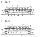
- Figs. 6 to 8 show variations of the semiconductor device shown in Fig. 1.
- semiconductor chips 3, 4, 5, and 6 are mounted, on the flip-chip basis, on an intermediate substrate 2 and are sealed with a resin 15, to form a semiconductor device, and the semiconductor device is mounted, on the flip-chip basis, on a printed wiring board 13 positioned outside the intermediate substrate 2 by means of external connection terminals 12 provided at a peripheral portion on one surface of the intermediate substrate 2.
- the semiconductor chips 3, 4, 5, and 6 are mounted, on the flip-chip basis, on the intermediate substrate 2 and the semiconductor device thus obtained is directly mounted, on the flip-chip basis, on the printed wiring board 13, it is possible to suppress the overall height of the semiconductor device, and hence to realize high density mounting of the semiconductor device.
- the variation shown in Fig. 7 is different from that shown in Fig. 6 in that an additional substrate 16 is provided between the intermediate substrate 2 and each external connection terminal 12 for enhancing the degree of freedom in connection to an external pin. With this configuration, it is possible to increase the mechanical strength of a PKG (package), and to reduce the number of interconnection layers of the intermediate substrate 2.
- the variation shown in Fig. 8 is different from that shown in Fig. 7 in that a reinforcement substrate 17 is provided between the additional substrate 16 and the external connection terminal 12 in such a manner as to cover the entire bottom surface of the intermediate substrate 2 for fixedly supporting a high frequency LSI chip 5 and a logic chip 6. With this configuration, it is possible to further enhance the mechanical strength and the reliability.
- semiconductor chips are mounted on both the surfaces of the intermediate substrate, it is possible to mixedly mount different semiconductor chips such as a logic chip, an analog chip, and a memory chip and hence to reduce the size of the semiconductor device and increase the level of integration of the semiconductor device.
- the contact between the chip and the intermediate substrate is not point-contact but nearly area-contact, to reduce the connection resistance therebetween, thereby significantly reducing a potential drop due to the resistances of the interconnections of the chip. This makes it possible to stabilize the power supply line, ground line, and signal line of the chip and hence to improve the electric characteristics of the chip.
- the realization of an LSI of a device operable at an ultra-low voltage such as a device using an SOI substrate is obstructed by the fact that the mixed mounting of a DRAM is very difficult in terms of its process technology and the fact that the operation of the device at an ultra-low voltage being significantly lower than 1 V cannot be ensured due to a potential drop caused by the large-scale integration; however, according to the present invention, the mixed mounting of a DRAM and the operation of the device at a ultra-low voltage can be simultaneously realized, and therefore, the present invention allows the device operable at an ultra-low voltage to be applied to the LSI system.
Abstract
Description
- The present invention relates to a semiconductor device including a plurality of semiconductor chips mounted on a substrate, and particularly to a semiconductor device suitable for realizing the reduction in size and weight of electronic equipment and the improvement of performances of the electronic equipment.
- Recently, to reduce sizes of semiconductor chips and increase the level of integration of the semiconductor chips, a technology of mixedly mounting a logic circuit, an analog circuit, and memories such as a DRAM and a flash memory on the same silicon substrate has been proposed and partially put into practical use.
- The technology of mixedly mounting semiconductor chips on the same silicon substrate, however, has various technical problems caused by evolution of a process of fabricating each of the semiconductor chips.
- For example, a thermal process necessary for forming a DRAM capacitor causes a problem in impairing an ultra-shallow junction profile essential for realizing a finer structure of a transistor in a logic chip, and also causes a problem in allowing boron in a gate electrode of a P-channel transistor to pass through a gate insulating film, to make a channel profile of the P-channel transistor different from a design profile, thereby degrading the current characteristics of the transistor.
- An analog circuit, which interfaces with external chips such as a driver, an amplifier and sensor, requires a higher withstand voltage and a higher input range than those of an advanced CMOS, and accordingly, the analog circuit is hard to be made finer in its geometrical structure. For a semiconductor chip in which the above analog circuit is integrated with a logic LSI required to be made very finer in its geometrical structure, most of the semiconductor chip is occupied by the analog circuit hard to be reduced in its area, to reduce an economical merit obtained by mixed mounting of the analog circuit and the logic circuit.
- In addition to the above technology of mixedly mounting semiconductor chips on the same silicon substrate, a technology of mixedly mounting semiconductor chips on a package level has been also positively promoted.
- A so-called chip-on-chip structure including semiconductor chips simply stacked to each other is advantageous in shortening lengths of interconnections; however, it is disadvantageous in sacrificing reinforcement of power source lines and ground lines in the chips. In an ultra-high speed CPU or DSP, an excessive current flowing in a chip reduces an effective inner voltage due to resistances of a power supply line and a ground line, to thereby reduce the operational speed.
- Even for a low power chip desired to realize operation at a significantly low supply voltage, the performance thereof may be significantly degraded by a slight reduction in potential due to resistances of interconnections. In particular, a chip desired to be operated at a voltage being as significantly low as 1 V or less, for example, a chip having a structure using an SOI (Si on insulator) substrate requires a very stable power supply line and a very stable ground line.
- Against such a background, power supply lines and ground lines of chips have been conventionally formed from multi-level interconnections, and in recent years, a technology of forming bonding pads corresponding to a plurality of power supply lines and ground lines in chips and connecting them to interconnections formed in a substrate, thereby further stabilizing the power supply lines and ground lines of the chips has been put in practical use.
- An object of the present invention is to provide a semiconductor device capable of mixedly mounting a logic chip, an analog chip, a memory chip, etc. by stacking them to each other while stabilizing power supply lines and ground lines of the chips.
- To achieve the above object, according to the present invention, there is provided a semiconductor device including: an intermediate substrate having a conductive portion and also having, on its one surface, an external connection terminal conducted to the conductive portion; and semiconductor chips each having connection portions, the semiconductor chips being mounted on both the surfaces of the intermediate substrate; wherein at least two of the semiconductor chips are electrically conducted to each other via the conductive portion of the intermediate substrate; and at least one of a power supply line, a ground line, and a signal line of each of the semiconductor chips is connected to the conductive portion of the intermediate substrate via two or more, conducted to each other, of the connection portions.
- With this configuration, since semiconductor chips such as a logic chip, an analog chip, a memory chip, etc. are mounted on both the surfaces of the intermediate substrate, it is possible to realize the mixed mounting of the semiconductor chips, and since at least one of the power supply line, ground line and signal line of each of the semiconductor chips thus mounted is connected to the conductive portion of the intermediate substrate via two or more, conducted to each other, of the connection portions, it is possible to stabilize the power supply lines, ground lines and signal lines of the semiconductor chips.
-
- Fig. 1 is a side view showing a schematic configuration of one embodiment of a semiconductor device of the present invention;
- Figs. 2A and 2B are bottom views each showing a configuration of connection portions of a semiconductor chip;
- Fig. 3A is a bottom view showing connection portions of a logic chip and a conductive pattern of the connection portions, and Fig. 3B is a plan view showing the surface of an intermediate substrate;
- Fig. 4 is a sectional side view of an essential portion of the intermediate substrate illustrating an example of multi-level interconnections of the intermediate substrate;
- Fig. 5 is a sectional side view showing a schematic configuration of another embodiment of the semiconductor device of the present invention;
- Fig. 6 is a side view showing a schematic configuration of one variation of the embodiment of the semiconductor device of the present invention shown in Fig. 1;
- Fig. 7 is a side view showing a schematic configuration of another variation of the embodiment of the semiconductor device of the present invention shown in Fig. 1; and
- Fig. 8 is a side view showing a schematic configuration of a further variation of the embodiment of the semiconductor device of the present invention shown in Fig. 1.
-
- Hereinafter, an embodiment of a semiconductor device of the present invention will be described in detail with reference to the drawings.
- Fig. 1 is a view showing one embodiment of a semiconductor device of the present invention. In this figure,
reference numeral 1 designates a semiconductor device. Thesemiconductor device 1 is a system LSI in which ananalog chip 3 and aDRAM chip 4 are mounted on one surface of anintermediate substrate 2 as shown in Fig. 2A, and a highfrequency LSI chip 5 and alogic chip 6 having a structure using an SOI substrate are mounted on the other surface of theintermediate substrate 2 as shown in Fig. 2B. - These
semiconductor chips logic chip 6, which requires high-speed and low power consumption operation at a low voltage, may be fabricated on the basis of a scaling law by using an advanced CMOS logic process allowing high level of integration. - The
DRAM chip 4 may be fabricated by using a general purpose DRAM process capable of realizing a large capacity at the least cost. - The
analog chip 3, which requires a higher withstand voltage and a higher input range in consideration of the interface relationship with peripheral chips, may be fabricated by a process which is required not to involve an advanced processing technology but to fabricate the chip at a cost lower than that of the logic chip. - The use of the
semiconductor chips - The connection structure of the
semiconductor device 1 will be more fully described below. Theintermediate substrate 2 has a conductive portion configured asmulti-level interconnections 7 made from copper, and each of thesemiconductor chips connection portions 8. Thesemiconductor chips intermediate substrate 2 via theconnection portions 8, and further, the electrical connection between these chips, that is, the electrical connection between power supply lines, ground lines and signal lines (not shown) of the chips are performed by themulti-level interconnections 7 of theintermediate substrate 2 via theconnection portions 8. - The
connection portions 8 of each of thesemiconductor chips connection portions 8 are connected to themulti-level interconnections 7 of theintermediate substrate 2 by means ofsolder ball bumps 9 as shown in Fig. 1. - The
connection portions 8 of each of thesemiconductor chips connection portions 8 are conducted to each other in the chip. In an example of thelogic chip 6 shown in Fig. 3A, a number of theconnection portions 8 disposed into an array are separated into groups connected to the power supply line, ground line, and signal line. The group of theconnection portions 8 connected to the power supply line are conducted to each other by means of aconductive pattern 10 formed in the silicon substrate. The group of theconnection portions 8 connected to the ground line are conducted to each other by means of aconductive pattern 11 formed in the silicon substrate. The group of theconnection portions 8 connected to the signal line (not shown) are conducted to each other by means of a conductive pattern (not shown) formed in the silicon substrate. - The group of the
connection portions 8 formed by the bonding pads, which are conducted to each other by means of theconductive pattern connection portions 8 form one areal pad as a whole. - As shown in Fig. 3B,
interconnection patterns multi-level interconnections 7 are formed on the surface of theintermediate substrate 2 in such a manner as to be matched to theconductive patterns connection portions 8 are disposed, respectively. Theconductive patterns corresponding interconnection patterns connection portions 8. - According to this embodiment, since each of the
semiconductor chips intermediate substrate 2 by means of theconnection portions 8 of the so-called area pad structure, the contact between the chip and theintermediate substrate 2 is not point-contact but nearly area-contact, to reduce the connection resistance therebetween, thereby stabilizing the power supply line, ground line, and signal line of the chip. - In general, the
interconnection patterns intermediate substrate 2 and themulti-level interconnections 7 connected thereto are sufficiently lower in resistance than the interconnections in each of thesemiconductor chips semiconductor chips multi-level interconnections 7 via theinterconnection patterns - The power supply lines, ground lines, and signal lines of the
semiconductor chips intermediate substrate 2 are collected via themulti-level interconnections 7 to a plurality ofexternal connection terminals 12 provided at a peripheral portion of one surface of theintermediate substrate 2. Theseexternal connection terminals 12 are used for mounting thesemiconductor device 1 to a printedwiring board 13 while being connected to wiring portions (not shown) of the printedwiring board 13. With this configuration, the power supply lines, ground lines, and signal lines of thesemiconductor chips wiring board 13 via theconnection portions 8 of the chips,interconnection patterns intermediate substrate 2,multi-level interconnections 7, and theexternal connection terminals 12, and are connected to wiring portions of electric equipment on which the printedwiring board 13 is mounted. - The configuration of the
multi-level interconnections 7 will be described with reference to an example shown in Fig. 4, in which theDRAM chip 4 configured as a general purpose DRAM bare chip is mounted on the upper surface of theintermediate substrate 2, and thelogic chip 6 is mounted on the back surface of theintermediate substrate 2. In this example, since the connection portions 8 (interface terminals) of theDRAM chip 4 are partially deviated from theConnection portions 8 of thelogic chip 6, the interconnections of thesechips intermediate substrate 2 in such a manner as to correct the above positional deviation between both thechips - The
multi-level interconnections 7 shown in Fig. 4 can connect the chips to each other via the interconnection patterns (not shown) formed on the surface of theintermediate substrate 2 in such a manner as to enhance the degree of freedom in connection and minimize the connection lengths. - Even in this example, the
semiconductor chips intermediate substrate 2 by connecting solder ball bumps 9 to theconnection portions 8 configured as the bonding pads. - According to the
semiconductor device 1 having the above configuration, since thesemiconductor chips intermediate substrate 2, it is possible to mixedly mount different semiconductor chips such as thelogic chip 3,DRAM chip 4, highfrequency LSI chip 5, andlogic chip 6 and hence to reduce the size of thesemiconductor device 1 and increase the level of integration of thesemiconductor device 1. - Since the power supply line, ground line, and signal line of each of the
semiconductor chips multi-level interconnections 7 of theintermediate substrate 2 via a group, conducted to each other, of theconnection portions 8, the contact between the chip and theintermediate substrate 2 is not point-contact but nearly area-contact, to reduce the connection resistance therebetween. This makes it possible to significantly reduce a potential drop due to the resistances of the interconnections of the chip, thereby stabilizing the power supply line, ground line, and signal line of the chip. - To be more specific, for a conventional semiconductor chip in which a power supply line or a ground line made from copper having a thickness of 1.5 µm and a width of 100 µm is used as an interconnection on the uppermost layer, the resistance per unit interconnection length (10 mm) is 1.3 Ω, and a potential drop caused when a current of 500 mA is applied to the interconnection reaches 0.65 V. Accordingly, it is difficult to design a low power LSI operable at a voltage being as small as 1 V.
- On the contrary, in the embodiment of the present invention shown in Fig. 1, the resistance per unit length (10 mm) of the interconnection on the
intermediate substrate 2 having a thickness of 50 µm and a width of 100 µm is 36 mΩ, and a potential drop when a current of 500 mA is applied to the interconnection is suppressed at 18 mV. - The interconnection layers of the semiconductor chips are connected to the
intermediate substrate 2 with a pitch of 300 µm, the maximum potential drop is about 28 mV (0.65 V × 0.3 mm/10 mm/2 + 18 mV). Accordingly, since the potential drop is very smaller, it is possible to design a low power LSI operable at a voltage being as small as 1 V. - The terminal capacitance upon conventional board mounting is about 10 pF; however, the interconnection capacitance between both chips mounted on the
intermediate substrate 2 becomes one-fifth the terminal capacitance, more concretely, about 2 pF per unit interconnection distance (10 mm). - The reduction in power has been achieved by mixedly mounting a DRAM; however, according to the present invention, it is possible to achieve the reduction in power comparable to that obtained in the case of mixedly mounting the DRAM by connecting a
specialized logic chip 6 to aspecialized DRAM chip 4 with the above low interconnection capacitance. - Since the power supply line, ground line, and signal line are each stabilized, a chip having the structure using an SOI substrate, which is mounted as the
logic chip 6, can be operated at a voltage being very lower than 1 V. Further, since the capacitance of a BUS equivalent to mixed mounting of a DRAM chip can be reduced, there can be obtained a device structure expected to minimize the power consumption. - While the
connection portions 8 of thesemiconductor chips intermediate substrate 2 by means of the solder ball bumps 9 in the above embodiment, the present invention is not limited thereto. For example, theconnection portions 8 may be connected to theintermediate substrate 2 by means of an anisotropic conductive film (ACF) 14 as shown in Fig. 5. The anisotropicconductive film 14 allows electric connection between theconnection portions 8 and theintermediate substrate 2 by applying heat and pressure thereto. The use of the anisotropicconductive film 14 allows a region in which theconnection portions 8, that is, the bonding pads are present to be made electrically conductive in the vertical direction, and also allows adjacent two of theconnection portions 8 to be significantly simply separated from each other. - The conductive portion of the
intermediate substrate 2 is not limited to themulti-level interconnections 7 but may be a single layer interconnection. - Figs. 6 to 8 show variations of the semiconductor device shown in Fig. 1. In the variation shown in Fig. 6,
semiconductor chips intermediate substrate 2 and are sealed with aresin 15, to form a semiconductor device, and the semiconductor device is mounted, on the flip-chip basis, on a printedwiring board 13 positioned outside theintermediate substrate 2 by means ofexternal connection terminals 12 provided at a peripheral portion on one surface of theintermediate substrate 2. With this structure, since thesemiconductor chips intermediate substrate 2 and the semiconductor device thus obtained is directly mounted, on the flip-chip basis, on the printedwiring board 13, it is possible to suppress the overall height of the semiconductor device, and hence to realize high density mounting of the semiconductor device. - The variation shown in Fig. 7 is different from that shown in Fig. 6 in that an
additional substrate 16 is provided between theintermediate substrate 2 and eachexternal connection terminal 12 for enhancing the degree of freedom in connection to an external pin. With this configuration, it is possible to increase the mechanical strength of a PKG (package), and to reduce the number of interconnection layers of theintermediate substrate 2. - The variation shown in Fig. 8 is different from that shown in Fig. 7 in that a
reinforcement substrate 17 is provided between theadditional substrate 16 and theexternal connection terminal 12 in such a manner as to cover the entire bottom surface of theintermediate substrate 2 for fixedly supporting a highfrequency LSI chip 5 and alogic chip 6. With this configuration, it is possible to further enhance the mechanical strength and the reliability. - As described above, according to the semiconductor device of the present invention, since semiconductor chips are mounted on both the surfaces of the intermediate substrate, it is possible to mixedly mount different semiconductor chips such as a logic chip, an analog chip, and a memory chip and hence to reduce the size of the semiconductor device and increase the level of integration of the semiconductor device.
- Since at least one of the power supply line, ground line, and signal line of each of the semiconductor chips thus mounted is connected to the conductive portion of the intermediate substrate via two or more, conducted to each other, of the connection portions, the contact between the chip and the intermediate substrate is not point-contact but nearly area-contact, to reduce the connection resistance therebetween, thereby significantly reducing a potential drop due to the resistances of the interconnections of the chip. This makes it possible to stabilize the power supply line, ground line, and signal line of the chip and hence to improve the electric characteristics of the chip.
- In particular, the realization of an LSI of a device operable at an ultra-low voltage such as a device using an SOI substrate is obstructed by the fact that the mixed mounting of a DRAM is very difficult in terms of its process technology and the fact that the operation of the device at an ultra-low voltage being significantly lower than 1 V cannot be ensured due to a potential drop caused by the large-scale integration; however, according to the present invention, the mixed mounting of a DRAM and the operation of the device at a ultra-low voltage can be simultaneously realized, and therefore, the present invention allows the device operable at an ultra-low voltage to be applied to the LSI system.
- While the preferred embodiment of the present invention has been described using the specific terms, such description is for illustrative purposes only, and it is to be understood that changes and variations may be made without departing from the spirit or scope of the following claims.
Claims (4)
- A semiconductor device comprising:an intermediate substrate having a conductive portion and also having, on its one surface, an external connection terminal conducted to said conductive portion; andsemiconductor chips each having connection portions, said semiconductor chips being mounted on both the surfaces of said intermediate substrate;
wherein at least two of said semiconductor chips are electrically conducted to each other via said conductive portion of said intermediate substrate; andat least one of a power supply line, a ground line, and a signal line of each of said semiconductor chips is connected to said conductive portion of said intermediate substrate via two or more, conducted to each other, of said connection portions. - A semiconductor device according to claim 1, wherein said connection portions of each of said semiconductor chips are connected to said conductive portion of said intermediate substrate by means of solder ball bumps.
- A semiconductor device according to claim 1, wherein said connection portions of each of said semiconductor chips are connected to said conductive portion of said intermediate substrate by means of an anisotropic conductive film.
- A semiconductor device according to claim 1, wherein at least one of said semiconductor chips is a chip having a structure using an SOI substrate.
Applications Claiming Priority (2)
| Application Number | Priority Date | Filing Date | Title |
|---|---|---|---|
| JP11191252A JP2001024150A (en) | 1999-07-06 | 1999-07-06 | Semiconductor device |
| JP19125299 | 1999-07-06 |
Publications (3)
| Publication Number | Publication Date |
|---|---|
| EP1067603A2 true EP1067603A2 (en) | 2001-01-10 |
| EP1067603A3 EP1067603A3 (en) | 2003-08-20 |
| EP1067603B1 EP1067603B1 (en) | 2006-03-29 |
Family
ID=16271451
Family Applications (1)
| Application Number | Title | Priority Date | Filing Date |
|---|---|---|---|
| EP00114291A Expired - Lifetime EP1067603B1 (en) | 1999-07-06 | 2000-07-04 | Chip carrier |
Country Status (7)
| Country | Link |
|---|---|
| US (1) | US6376917B1 (en) |
| EP (1) | EP1067603B1 (en) |
| JP (1) | JP2001024150A (en) |
| KR (1) | KR100697758B1 (en) |
| CA (1) | CA2313611C (en) |
| DE (1) | DE60026905T2 (en) |
| TW (1) | TW451454B (en) |
Cited By (3)
| Publication number | Priority date | Publication date | Assignee | Title |
|---|---|---|---|---|
| EP1137067A2 (en) * | 2000-03-20 | 2001-09-26 | Agere Systems Guardian Corporation | Multi-chip ball grid array ic packages |
| WO2003030255A2 (en) * | 2001-10-03 | 2003-04-10 | Formfactor, Inc. | Multiple die interconnect system |
| EP1744362A2 (en) * | 2005-07-15 | 2007-01-17 | Shinko Electric Industries Co., Ltd. | Semiconductor device and electronic apparatus |
Families Citing this family (49)
| Publication number | Priority date | Publication date | Assignee | Title |
|---|---|---|---|---|
| JP2960560B2 (en) | 1991-02-28 | 1999-10-06 | 株式会社日立製作所 | Microelectronic equipment |
| JP2001068621A (en) * | 1999-06-21 | 2001-03-16 | Shinko Electric Ind Co Ltd | Semiconductor device and its manufacture |
| US7394153B2 (en) * | 1999-12-17 | 2008-07-01 | Osram Opto Semiconductors Gmbh | Encapsulation of electronic devices |
| EP1240808B1 (en) * | 1999-12-17 | 2003-05-21 | Osram Opto Semiconductors GmbH | Encapsulation for organic led device |
| EP1242849B1 (en) | 1999-12-17 | 2007-02-21 | Osram Opto Semiconductors GmbH | Improved encapsulation for organic led device |
| TW569403B (en) * | 2001-04-12 | 2004-01-01 | Siliconware Precision Industries Co Ltd | Multi-chip module and its manufacturing method |
| JP3420748B2 (en) * | 2000-12-14 | 2003-06-30 | 松下電器産業株式会社 | Semiconductor device and manufacturing method thereof |
| US20020121707A1 (en) * | 2001-02-27 | 2002-09-05 | Chippac, Inc. | Super-thin high speed flip chip package |
| US8143108B2 (en) * | 2004-10-07 | 2012-03-27 | Stats Chippac, Ltd. | Semiconductor device and method of dissipating heat from thin package-on-package mounted to substrate |
| US20040070080A1 (en) * | 2001-02-27 | 2004-04-15 | Chippac, Inc | Low cost, high performance flip chip package structure |
| USRE44438E1 (en) | 2001-02-27 | 2013-08-13 | Stats Chippac, Ltd. | Semiconductor device and method of dissipating heat from thin package-on-package mounted to substrate |
| TW523889B (en) * | 2002-01-09 | 2003-03-11 | Advanced Semiconductor Eng | Semiconductor packaged device |
| KR100481706B1 (en) * | 2002-03-25 | 2005-04-11 | 주식회사 넥사이언 | Method of fabricating flip chip |
| US6911726B2 (en) * | 2002-06-07 | 2005-06-28 | Intel Corporation | Microelectronic packaging and methods for thermally protecting package interconnects and components |
| TW546796B (en) * | 2002-06-10 | 2003-08-11 | Advanced Semiconductor Eng | Multichip package |
| US7294928B2 (en) | 2002-09-06 | 2007-11-13 | Tessera, Inc. | Components, methods and assemblies for stacked packages |
| US6765152B2 (en) * | 2002-09-27 | 2004-07-20 | International Business Machines Corporation | Multichip module having chips on two sides |
| TW569416B (en) * | 2002-12-19 | 2004-01-01 | Via Tech Inc | High density multi-chip module structure and manufacturing method thereof |
| US20040262727A1 (en) * | 2003-06-30 | 2004-12-30 | Mcconville David P. | Computer system implemented on flex tape |
| JP4587676B2 (en) * | 2004-01-29 | 2010-11-24 | ルネサスエレクトロニクス株式会社 | Three-dimensional semiconductor device having a stacked chip configuration |
| JP2006303003A (en) * | 2005-04-18 | 2006-11-02 | Toshiba Corp | Printed board and information processing apparatus |
| JP4507101B2 (en) | 2005-06-30 | 2010-07-21 | エルピーダメモリ株式会社 | Semiconductor memory device and manufacturing method thereof |
| TWI264127B (en) * | 2005-09-23 | 2006-10-11 | Via Tech Inc | Chip package and substrate thereof |
| WO2007049375A1 (en) * | 2005-10-27 | 2007-05-03 | Murata Manufacturing Co., Ltd. | Composite circuit module and high-frequency module device |
| JP4844118B2 (en) * | 2005-12-22 | 2011-12-28 | パナソニック電工株式会社 | Sensor module and manufacturing method thereof |
| JP2008091638A (en) | 2006-10-02 | 2008-04-17 | Nec Electronics Corp | Electronic equipment, and manufacturing method thereof |
| US8237289B2 (en) | 2007-01-30 | 2012-08-07 | Kabushiki Kaisha Toshiba | System in package device |
| JP2008294423A (en) | 2007-04-24 | 2008-12-04 | Nec Electronics Corp | Semiconductor device |
| CN101471330B (en) * | 2007-12-28 | 2010-06-09 | 鸿富锦精密工业(深圳)有限公司 | Semiconductor encapsulation structure |
| KR101193416B1 (en) * | 2008-05-09 | 2012-10-24 | 고쿠리츠 다이가쿠 호진 큐슈 코교 다이가쿠 | Three-dimensionally integrated semiconductor device and method for manufacturing the same |
| US8399983B1 (en) * | 2008-12-11 | 2013-03-19 | Xilinx, Inc. | Semiconductor assembly with integrated circuit and companion device |
| JP4801133B2 (en) * | 2008-12-15 | 2011-10-26 | ルネサスエレクトロニクス株式会社 | Semiconductor device |
| US8987896B2 (en) * | 2009-12-16 | 2015-03-24 | Intel Corporation | High-density inter-package connections for ultra-thin package-on-package structures, and processes of forming same |
| JP5091221B2 (en) * | 2009-12-28 | 2012-12-05 | ルネサスエレクトロニクス株式会社 | Semiconductor device |
| US20130277855A1 (en) * | 2012-04-24 | 2013-10-24 | Terry (Teckgyu) Kang | High density 3d package |
| JP6005438B2 (en) * | 2012-08-10 | 2016-10-12 | 株式会社ThruChip Japan | Stacked integrated circuit |
| KR101950976B1 (en) * | 2012-10-25 | 2019-02-25 | 에스케이하이닉스 주식회사 | Semiconductor package |
| US20140159758A1 (en) * | 2012-12-12 | 2014-06-12 | Qualcomm Incorporated | Assembly for optical backside failure analysis of package-on-package (pop) during electrical testing |
| US9070657B2 (en) * | 2013-10-08 | 2015-06-30 | Freescale Semiconductor, Inc. | Heat conductive substrate for integrated circuit package |
| EP2881983B1 (en) | 2013-12-05 | 2019-09-18 | ams AG | Interposer-chip-arrangement for dense packaging of chips |
| EP2881753B1 (en) | 2013-12-05 | 2019-03-06 | ams AG | Optical sensor arrangement and method of producing an optical sensor arrangement |
| US10354984B2 (en) | 2015-05-27 | 2019-07-16 | Bridge Semiconductor Corporation | Semiconductor assembly with electromagnetic shielding and thermally enhanced characteristics and method of making the same |
| US10121768B2 (en) | 2015-05-27 | 2018-11-06 | Bridge Semiconductor Corporation | Thermally enhanced face-to-face semiconductor assembly with built-in heat spreader and method of making the same |
| US11291146B2 (en) | 2014-03-07 | 2022-03-29 | Bridge Semiconductor Corp. | Leadframe substrate having modulator and crack inhibiting structure and flip chip assembly using the same |
| JP6019367B2 (en) * | 2015-01-13 | 2016-11-02 | 株式会社野田スクリーン | Semiconductor device |
| US20190006339A1 (en) * | 2017-06-28 | 2019-01-03 | Asm Technology Singapore Pte Ltd | Three-dimensional integrated fan-out wafer level package |
| JP2018137474A (en) * | 2018-04-16 | 2018-08-30 | ルネサスエレクトロニクス株式会社 | Electronic apparatus |
| WO2020101572A1 (en) * | 2018-11-12 | 2020-05-22 | Agency For Science, Technology And Research | Multi-chip system and method of forming the same |
| CN112543559A (en) * | 2020-12-08 | 2021-03-23 | 福建飞毛腿动力科技有限公司 | Flow-expanding and flow-guiding welded plate based on aluminum substrate patch and flow equalizing method thereof |
Citations (9)
| Publication number | Priority date | Publication date | Assignee | Title |
|---|---|---|---|---|
| EP0242303A2 (en) * | 1986-04-17 | 1987-10-21 | Digital Equipment Corporation | Anisotropic elastomeric interconnecting system |
| EP0424106A2 (en) * | 1989-10-17 | 1991-04-24 | Sharp Kabushiki Kaisha | A method for connecting circuit boards |
| EP0486829A2 (en) * | 1990-10-22 | 1992-05-27 | Seiko Epson Corporation | Semiconductor device and semiconductor device packaging system |
| EP0527044A1 (en) * | 1991-08-05 | 1993-02-10 | International Business Machines Corporation | Memory package |
| US5477082A (en) * | 1994-01-11 | 1995-12-19 | Exponential Technology, Inc. | Bi-planar multi-chip module |
| US5801072A (en) * | 1996-03-14 | 1998-09-01 | Lsi Logic Corporation | Method of packaging integrated circuits |
| US5805424A (en) * | 1996-09-24 | 1998-09-08 | Texas Instruments Incorporated | Microelectronic assemblies including Z-axis conductive films |
| US5838072A (en) * | 1997-02-24 | 1998-11-17 | Mosel Vitalic Corporation | Intrachip power distribution package and method for semiconductors having a supply node electrically interconnected with one or more intermediate nodes |
| US5892275A (en) * | 1995-08-29 | 1999-04-06 | Intel Corporation | High performance power and ground edge connect IC package |
Family Cites Families (6)
| Publication number | Priority date | Publication date | Assignee | Title |
|---|---|---|---|---|
| US5396403A (en) * | 1993-07-06 | 1995-03-07 | Hewlett-Packard Company | Heat sink assembly with thermally-conductive plate for a plurality of integrated circuits on a substrate |
| US6133637A (en) * | 1997-01-24 | 2000-10-17 | Rohm Co., Ltd. | Semiconductor device having a plurality of semiconductor chips |
| US6075287A (en) * | 1997-04-03 | 2000-06-13 | International Business Machines Corporation | Integrated, multi-chip, thermally conductive packaging device and methodology |
| US6150724A (en) * | 1998-03-02 | 2000-11-21 | Motorola, Inc. | Multi-chip semiconductor device and method for making the device by using multiple flip chip interfaces |
| US5977640A (en) * | 1998-06-26 | 1999-11-02 | International Business Machines Corporation | Highly integrated chip-on-chip packaging |
| KR100527044B1 (en) * | 2003-10-28 | 2005-11-09 | 주식회사 한국종합기술개발공사 | Electric pole for prevention of electric shock accident |
-
1999
- 1999-07-06 JP JP11191252A patent/JP2001024150A/en active Pending
-
2000
- 2000-07-04 TW TW089113178A patent/TW451454B/en not_active IP Right Cessation
- 2000-07-04 DE DE60026905T patent/DE60026905T2/en not_active Expired - Lifetime
- 2000-07-04 EP EP00114291A patent/EP1067603B1/en not_active Expired - Lifetime
- 2000-07-05 CA CA2313611A patent/CA2313611C/en not_active Expired - Lifetime
- 2000-07-06 KR KR1020000038519A patent/KR100697758B1/en active IP Right Grant
- 2000-07-06 US US09/611,205 patent/US6376917B1/en not_active Expired - Lifetime
Patent Citations (10)
| Publication number | Priority date | Publication date | Assignee | Title |
|---|---|---|---|---|
| US4778950A (en) * | 1985-07-22 | 1988-10-18 | Digital Equipment Corporation | Anisotropic elastomeric interconnecting system |
| EP0242303A2 (en) * | 1986-04-17 | 1987-10-21 | Digital Equipment Corporation | Anisotropic elastomeric interconnecting system |
| EP0424106A2 (en) * | 1989-10-17 | 1991-04-24 | Sharp Kabushiki Kaisha | A method for connecting circuit boards |
| EP0486829A2 (en) * | 1990-10-22 | 1992-05-27 | Seiko Epson Corporation | Semiconductor device and semiconductor device packaging system |
| EP0527044A1 (en) * | 1991-08-05 | 1993-02-10 | International Business Machines Corporation | Memory package |
| US5477082A (en) * | 1994-01-11 | 1995-12-19 | Exponential Technology, Inc. | Bi-planar multi-chip module |
| US5892275A (en) * | 1995-08-29 | 1999-04-06 | Intel Corporation | High performance power and ground edge connect IC package |
| US5801072A (en) * | 1996-03-14 | 1998-09-01 | Lsi Logic Corporation | Method of packaging integrated circuits |
| US5805424A (en) * | 1996-09-24 | 1998-09-08 | Texas Instruments Incorporated | Microelectronic assemblies including Z-axis conductive films |
| US5838072A (en) * | 1997-02-24 | 1998-11-17 | Mosel Vitalic Corporation | Intrachip power distribution package and method for semiconductors having a supply node electrically interconnected with one or more intermediate nodes |
Cited By (9)
| Publication number | Priority date | Publication date | Assignee | Title |
|---|---|---|---|---|
| EP1137067A2 (en) * | 2000-03-20 | 2001-09-26 | Agere Systems Guardian Corporation | Multi-chip ball grid array ic packages |
| EP1137067A3 (en) * | 2000-03-20 | 2007-09-26 | Agere Systems Guardian Corporation | Multi-chip ball grid array ic packages |
| WO2003030255A2 (en) * | 2001-10-03 | 2003-04-10 | Formfactor, Inc. | Multiple die interconnect system |
| WO2003030255A3 (en) * | 2001-10-03 | 2003-10-30 | Formfactor Inc | Multiple die interconnect system |
| KR100935838B1 (en) * | 2001-10-03 | 2010-01-08 | 폼팩터, 인크. | Multiple die interconnect system |
| US7681309B2 (en) | 2001-10-03 | 2010-03-23 | Formfactor, Inc. | Method for interconnecting an integrated circuit multiple die assembly |
| EP1744362A2 (en) * | 2005-07-15 | 2007-01-17 | Shinko Electric Industries Co., Ltd. | Semiconductor device and electronic apparatus |
| EP1744362A3 (en) * | 2005-07-15 | 2010-01-20 | Shinko Electric Industries Co., Ltd. | Semiconductor device and electronic apparatus |
| US8169073B2 (en) | 2005-07-15 | 2012-05-01 | Shinko Electric Industries Co., Ltd. | Semiconductor device and electronic apparatus of multi-chip packaging |
Also Published As
| Publication number | Publication date |
|---|---|
| TW451454B (en) | 2001-08-21 |
| EP1067603A3 (en) | 2003-08-20 |
| EP1067603B1 (en) | 2006-03-29 |
| DE60026905T2 (en) | 2006-12-14 |
| CA2313611C (en) | 2010-05-18 |
| JP2001024150A (en) | 2001-01-26 |
| DE60026905D1 (en) | 2006-05-18 |
| KR20010066905A (en) | 2001-07-11 |
| CA2313611A1 (en) | 2001-01-06 |
| US6376917B1 (en) | 2002-04-23 |
| KR100697758B1 (en) | 2007-03-21 |
Similar Documents
| Publication | Publication Date | Title |
|---|---|---|
| US6376917B1 (en) | Semiconductor device | |
| US6507115B2 (en) | Multi-chip integrated circuit module | |
| US7005747B2 (en) | Semiconductor device having additional functional element and method of manufacturing thereof | |
| US6853058B2 (en) | Process for providing electrical connection between a semiconductor die and a semiconductor die receiving member | |
| US8466564B2 (en) | Enhanced stacked microelectronic assemblies with central contacts and improved ground or power distribution | |
| US6075712A (en) | Flip-chip having electrical contact pads on the backside of the chip | |
| US7463492B2 (en) | Array capacitors with voids to enable a full-grid socket | |
| EP3073525B1 (en) | Semiconductor package assembly with a metal-insulator-metal capacitor structure | |
| US8097954B2 (en) | Adhesive layer forming a capacitor dielectric between semiconductor chips | |
| US5606199A (en) | Resin-molded type semiconductor device with tape carrier connection between chip electrodes and inner leads of lead frame | |
| US7023085B2 (en) | Semiconductor package structure with reduced parasite capacitance and method of fabricating the same | |
| JPH0587977B2 (en) | ||
| US6340839B1 (en) | Hybrid integrated circuit | |
| JP2000124352A (en) | Semiconductor integrated circuit device and manufacture thereof | |
| JP2008124072A (en) | Semiconductor device | |
| US9721928B1 (en) | Integrated circuit package having two substrates | |
| US6965163B2 (en) | Substrate-less microelectronic package | |
| US6020631A (en) | Method and apparatus for connecting a bondwire to a bondring near a via | |
| US20030080418A1 (en) | Semiconductor device having power supply pads arranged between signal pads and substrate edge | |
| JP4370993B2 (en) | Semiconductor device | |
| KR20010067308A (en) | Integrated circuit package with stacked dies | |
| GB2285335A (en) | Semiconductor device | |
| KR20050027384A (en) | Chip size package having rerouting pad and stack thereof | |
| CN117116905A (en) | Semiconductor device and method for manufacturing the same | |
| JP3574004B2 (en) | Semiconductor device |
Legal Events
| Date | Code | Title | Description |
|---|---|---|---|
| PUAI | Public reference made under article 153(3) epc to a published international application that has entered the european phase |
Free format text: ORIGINAL CODE: 0009012 |
|
| AK | Designated contracting states |
Kind code of ref document: A2 Designated state(s): AT BE CH CY DE DK ES FI FR GB GR IE IT LI LU MC NL PT SE |
|
| AX | Request for extension of the european patent |
Free format text: AL;LT;LV;MK;RO;SI |
|
| PUAL | Search report despatched |
Free format text: ORIGINAL CODE: 0009013 |
|
| AK | Designated contracting states |
Designated state(s): AT BE CH CY DE DK ES FI FR GB GR IE IT LI LU MC NL PT SE |
|
| AX | Request for extension of the european patent |
Extension state: AL LT LV MK RO SI |
|
| 17P | Request for examination filed |
Effective date: 20040123 |
|
| 17Q | First examination report despatched |
Effective date: 20040224 |
|
| AKX | Designation fees paid |
Designated state(s): DE FR GB |
|
| GRAC | Information related to communication of intention to grant a patent modified |
Free format text: ORIGINAL CODE: EPIDOSCIGR1 |
|
| GRAP | Despatch of communication of intention to grant a patent |
Free format text: ORIGINAL CODE: EPIDOSNIGR1 |
|
| GRAS | Grant fee paid |
Free format text: ORIGINAL CODE: EPIDOSNIGR3 |
|
| GRAA | (expected) grant |
Free format text: ORIGINAL CODE: 0009210 |
|
| AK | Designated contracting states |
Kind code of ref document: B1 Designated state(s): DE FR GB |
|
| REG | Reference to a national code |
Ref country code: GB Ref legal event code: FG4D |
|
| REF | Corresponds to: |
Ref document number: 60026905 Country of ref document: DE Date of ref document: 20060518 Kind code of ref document: P |
|
| ET | Fr: translation filed | ||
| PLBE | No opposition filed within time limit |
Free format text: ORIGINAL CODE: 0009261 |
|
| STAA | Information on the status of an ep patent application or granted ep patent |
Free format text: STATUS: NO OPPOSITION FILED WITHIN TIME LIMIT |
|
| 26N | No opposition filed |
Effective date: 20070102 |
|
| REG | Reference to a national code |
Ref country code: GB Ref legal event code: 746 Effective date: 20091130 |
|
| REG | Reference to a national code |
Ref country code: FR Ref legal event code: PLFP Year of fee payment: 17 |
|
| REG | Reference to a national code |
Ref country code: FR Ref legal event code: PLFP Year of fee payment: 18 |
|
| REG | Reference to a national code |
Ref country code: FR Ref legal event code: PLFP Year of fee payment: 19 |
|
| PGFP | Annual fee paid to national office [announced via postgrant information from national office to epo] |
Ref country code: DE Payment date: 20190719 Year of fee payment: 20 Ref country code: FR Payment date: 20190719 Year of fee payment: 20 |
|
| PGFP | Annual fee paid to national office [announced via postgrant information from national office to epo] |
Ref country code: GB Payment date: 20190719 Year of fee payment: 20 |
|
| REG | Reference to a national code |
Ref country code: DE Ref legal event code: R071 Ref document number: 60026905 Country of ref document: DE |
|
| REG | Reference to a national code |
Ref country code: GB Ref legal event code: PE20 Expiry date: 20200703 |
|
| PG25 | Lapsed in a contracting state [announced via postgrant information from national office to epo] |
Ref country code: GB Free format text: LAPSE BECAUSE OF EXPIRATION OF PROTECTION Effective date: 20200703 |