EP1069453B1 - Vorrichtung zur Reduzierung der Peakleistung einer Pulslaser-Lichtquelle - Google Patents
Vorrichtung zur Reduzierung der Peakleistung einer Pulslaser-Lichtquelle Download PDFInfo
- Publication number
- EP1069453B1 EP1069453B1 EP00112846A EP00112846A EP1069453B1 EP 1069453 B1 EP1069453 B1 EP 1069453B1 EP 00112846 A EP00112846 A EP 00112846A EP 00112846 A EP00112846 A EP 00112846A EP 1069453 B1 EP1069453 B1 EP 1069453B1
- Authority
- EP
- European Patent Office
- Prior art keywords
- laser light
- light source
- diversion line
- pulse laser
- path
- Prior art date
- Legal status (The legal status is an assumption and is not a legal conclusion. Google has not performed a legal analysis and makes no representation as to the accuracy of the status listed.)
- Expired - Lifetime
Links
Images


Classifications
-
- H—ELECTRICITY
- H01—ELECTRIC ELEMENTS
- H01S—DEVICES USING THE PROCESS OF LIGHT AMPLIFICATION BY STIMULATED EMISSION OF RADIATION [LASER] TO AMPLIFY OR GENERATE LIGHT; DEVICES USING STIMULATED EMISSION OF ELECTROMAGNETIC RADIATION IN WAVE RANGES OTHER THAN OPTICAL
- H01S3/00—Lasers, i.e. devices using stimulated emission of electromagnetic radiation in the infrared, visible or ultraviolet wave range
- H01S3/10—Controlling the intensity, frequency, phase, polarisation or direction of the emitted radiation, e.g. switching, gating, modulating or demodulating
-
- G—PHYSICS
- G03—PHOTOGRAPHY; CINEMATOGRAPHY; ANALOGOUS TECHNIQUES USING WAVES OTHER THAN OPTICAL WAVES; ELECTROGRAPHY; HOLOGRAPHY
- G03F—PHOTOMECHANICAL PRODUCTION OF TEXTURED OR PATTERNED SURFACES, e.g. FOR PRINTING, FOR PROCESSING OF SEMICONDUCTOR DEVICES; MATERIALS THEREFOR; ORIGINALS THEREFOR; APPARATUS SPECIALLY ADAPTED THEREFOR
- G03F7/00—Photomechanical, e.g. photolithographic, production of textured or patterned surfaces, e.g. printing surfaces; Materials therefor, e.g. comprising photoresists; Apparatus specially adapted therefor
- G03F7/70—Microphotolithographic exposure; Apparatus therefor
- G03F7/70483—Information management; Active and passive control; Testing; Wafer monitoring, e.g. pattern monitoring
- G03F7/7055—Exposure light control in all parts of the microlithographic apparatus, e.g. pulse length control or light interruption
-
- G—PHYSICS
- G02—OPTICS
- G02B—OPTICAL ELEMENTS, SYSTEMS OR APPARATUS
- G02B27/00—Optical systems or apparatus not provided for by any of the groups G02B1/00 - G02B26/00, G02B30/00
- G02B27/10—Beam splitting or combining systems
- G02B27/106—Beam splitting or combining systems for splitting or combining a plurality of identical beams or images, e.g. image replication
-
- G—PHYSICS
- G02—OPTICS
- G02B—OPTICAL ELEMENTS, SYSTEMS OR APPARATUS
- G02B27/00—Optical systems or apparatus not provided for by any of the groups G02B1/00 - G02B26/00, G02B30/00
- G02B27/10—Beam splitting or combining systems
- G02B27/14—Beam splitting or combining systems operating by reflection only
- G02B27/144—Beam splitting or combining systems operating by reflection only using partially transparent surfaces without spectral selectivity
-
- G—PHYSICS
- G02—OPTICS
- G02B—OPTICAL ELEMENTS, SYSTEMS OR APPARATUS
- G02B27/00—Optical systems or apparatus not provided for by any of the groups G02B1/00 - G02B26/00, G02B30/00
- G02B27/10—Beam splitting or combining systems
- G02B27/14—Beam splitting or combining systems operating by reflection only
- G02B27/145—Beam splitting or combining systems operating by reflection only having sequential partially reflecting surfaces
-
- G—PHYSICS
- G03—PHOTOGRAPHY; CINEMATOGRAPHY; ANALOGOUS TECHNIQUES USING WAVES OTHER THAN OPTICAL WAVES; ELECTROGRAPHY; HOLOGRAPHY
- G03F—PHOTOMECHANICAL PRODUCTION OF TEXTURED OR PATTERNED SURFACES, e.g. FOR PRINTING, FOR PROCESSING OF SEMICONDUCTOR DEVICES; MATERIALS THEREFOR; ORIGINALS THEREFOR; APPARATUS SPECIALLY ADAPTED THEREFOR
- G03F7/00—Photomechanical, e.g. photolithographic, production of textured or patterned surfaces, e.g. printing surfaces; Materials therefor, e.g. comprising photoresists; Apparatus specially adapted therefor
- G03F7/20—Exposure; Apparatus therefor
- G03F7/2002—Exposure; Apparatus therefor with visible light or UV light, through an original having an opaque pattern on a transparent support, e.g. film printing, projection printing; by reflection of visible or UV light from an original such as a printed image
- G03F7/2008—Exposure; Apparatus therefor with visible light or UV light, through an original having an opaque pattern on a transparent support, e.g. film printing, projection printing; by reflection of visible or UV light from an original such as a printed image characterised by the reflectors, diffusers, light or heat filtering means or anti-reflective means used
Definitions
- the invention relates to a projection exposure system with a device for reducing the Peak power of a pulse laser light source.
- Pulse laser light sources e.g. Excimer laser
- UV lithography have a repetition rate of approximately 1000 to 4000 Pulses per second.
- the pulse length is currently 20 to 30 ns.
- Within each pulse there is dependence from the gas state, from the state of the laser, especially the optical one Components, and depending on the resonator length to considerable Modulations of the laser output power over the Time.
- a clear disadvantage of a pulse laser light source is that the short pulse duration causes a high pulse power density, which has a very negative effect on the optical materials, in particular glassy materials. Quartz glass at a working wavelength of 193 nm is damaged at a rate that includes a power density power. The consequences of this are transmission losses and an uncontrolled increase in the refractive index, which limits the life of the optical system. SiO 2 in glassy form has areas with particularly weak bonds. The pulsed short-wave electromagnetic radiation generated by the pulse laser light source thus supplies the energy in order to disadvantageously modify these locations.
- EP 0 785 473 A2 describes a device of the type mentioned at the beginning kind known by which from a pulse laser light source incoming light divided into several partial beams which detours are going through. This is done a bundle expansion or a division into several partial beams arranged side by side. These partial beams are arranged side by side in a lighting device entered.
- US-A 5 337 333 relates to a reduction device the peak power of a pulse laser light source for X-ray lithography.
- US-A 4 941 093 describes a laser for beam shaping for eroding a surface, being in the machining beam a telescope consisting of two converging lenses, is arranged to the laser beam to the requirements to optimize.
- the present invention is therefore based on the object to create a device with the help of damage from Components that lie in the beam path of the pulse laser light source, to be avoided, if possible without any particular loss the efficiency of the pulse laser light source.
- the beam of the pulse laser light source is divided in partial beams with an optical path difference. It is just to make sure that the gear difference is chosen so is that peaks and valleys complement each other at least largely. Peaks and valleys are separated in time, e.g. 7.0 ns. This corresponds to a light path of 2.1 m.
- at least two detour lines of the invention to be arranged one behind the other in the beam path.
- partial beams are not generated are arranged side by side with a corresponding number of optical axes, but there is a reunification of the partial beams to form an overall beam, making a uniform one optical axis for the subsequent lighting device given is. It takes place after the division into several Finally, partial beams are threaded again.
- the invention Device breeds for influencing polarized light insert what for between the beam path and the Beam splitter device an angle, namely the Brewster angle in conjunction with a slightly detuned Kepler telescope, is provided.
- the Brewster angle means that that by the beam splitter device, e.g. one Mirror, 50% of the beam pass freely and without loss (apart from absorption in the dividing layer), while the other 50% are derived.
- the beam splitter device e.g. one Mirror
- 50% of the beam pass freely and without loss (apart from absorption in the dividing layer), while the other 50% are derived.
- the beam splitter device e.g. one Mirror
- the beam combining member is designed such that part of the sub-beam that passed through the detour line is sent repeatedly via the detour line.
- a phase delay plate in the beam path gives an influence on the power peaks and the service life the optical materials exposed to the pulse laser light source are.
- a beam of rays 1 strikes a pulse laser light source, e.g. an excimer laser 2 (shown in Figure 5) to a first beam splitter device in the form of a mirror 3. pass 50% of the total beam as a partial beam 1a, the divider mirror is unhindered and loss-free 3 towards a second divider mirror 4 as second beam splitter device. The other 50% of the beam take their path as partial beam 1b via a detour line 5, by three mirrors 6, 7 and 8 as reflective components is formed.
- the splitter mirror 3 as the first beam splitter device acts on the back as well Beam combining element 9, in which the partial beam 1b with the partial beam passing through the beam splitter device la is reunited.
- the pulse of the pulse laser light source 2 is smoothed.
- the peak performance is reduced by 30 to 40% reduced. Due to the angular position of the divider mirror 3 or the first detour line 5 to the direction of vibration of the incident linearly polarized laser light plays the height of the Degree of polarization does not matter for the energy balance.
- Both Partial beams 1a and 1b are at the exit of the first detour line 5 polarized equally, but staggered in time.
- the time offset of the two partial beams is shown in FIG 1a and 1b recognizable.
- the Peak power of the pulse laser light source, due to the Beam splitting has been reduced to half each an addition due to the time offset of the two "Peaks" P1 and P2 respectively in the resulting one Total peak compared to an untreated beam path reduced.
- the laser light beam comes after the two reunited Partial beams 1a and 1b in the further beam path through the second beam splitter device in the form of the splitter mirror 4, which in turn turned 45 ° (Brewster angle) to the direction of vibration of the laser light lies in the partial beam 10a passes the splitter mirror 4 unhindered, and the partial beam 10b, which is sent via a second detour line 11, divided.
- the second detour line 11 is also mirrored 12, 13 and 14 formed as reflective components.
- the back of the beam splitter 4 again serves as the second Beam combining member 15 through which the two partial beams 10a and 10b reassembled with the same polarization direction and then forwarded together.
- the pulse of the pulse laser light source 2 offset as a whole. This way you get at the exit or on the beam combining member 15 two pulses with the same Polarization that is largely smoothed or none is not permitted have high "peaks" that cause damage to Components could lead.
- Figure 3 shows the power over time and the two Pulses can be seen as they come after the beam combining element 15 available.
- the original peak performance can be about a third of the original value will be reduced.
- the temporal pulse duration of the pulse laser light source 30 ns this corresponds to a path of the light of 9 m.
- first detour line 5 with the second detour line 11 so once delayed by 2.1 m and the pulse smoothed in this way 9.0 m + 2.1 m, i.e. a total of 11.1 m delayed in the second detour line 11.
- Areas are best suited for the measures according to the invention between the laser output and a scanner input.
- the particular advantage of the invention is that the subsequent lighting unit are not specially designed must, but only the proposed facility between the laser output and the input of the lighting part Scanner is inserted. It also becomes an economic one Retrofitting of existing systems possible (no new lighting part of the scanner).
- FIG. 4 shows a further embodiment of a Detour line shown in principle.
- the beam splitter device 3 passes through the beam splitter device 3, and one Partial beam 1b, which is the path via the rectangular detour line 5 takes.
- the detour line 5 is through four mirrors 17, 18, 19 and 20 formed before the partial beam 1b on the back the beam splitter device 3, which as well as in the Embodiment according to Figure 1 as a beam union 9 is used, is again combined with the partial beam 1a.
- the embodiment according to FIG. 4 is designed that a portion of the partial beam passed through the detour line 5 1b the route again via the detour line 5 takes, which can be done multiple times.
- the coupling the beam takes place in this embodiment in the manner of a resonator, the proportion of the via the detour 5 circulating light or partial beam 1b, i.e. the adjustable pulse length, from the state of polarization depends. In this way, any delays in the incoming pulses and a related reduction in the Pulse peak energy of the pulse laser light source can be achieved.
- the configuration according to FIG. 4 with the two phase delay plates 21 and 22 has the advantage of doing this the device can be used very variably. switches namely one or both phase delay plates 21 or 22 off, the peak power changes accordingly.
- switches namely one or both phase delay plates 21 or 22 off the peak power changes accordingly.
- you can also use a corresponding increase in the number of revolutions of light one Protection of the optical components of the projection exposure system to reach.
- FIG. 5 the point of use of FIG. 5 is Device 23 shown.
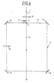
- the polarized Light source 2 is then for a projection exposure system provided, which is in a by a wall 17 of separate clean room with lighting optics 18, a mask 19, a projection lens 20 and a laser 21 is located.
- the device 23, which is inside with the parts shown in Figure 1 is provided between the Pulse laser light source 2 and the wall 17 in the beam path 1 the pulse laser light source 2 is arranged.
Description
- Figur 1
- eine Prinzipdarstellung des Strahlenganges einer Pulslaser-Lichtquelle mit zwei Umwegleitungen;
- Figur 2
- die Leistung der Pulslaser-Lichtquelle im Aufteilungszustand durch eine erste Umwegleitung;
- Figur 3
- den Leistungsverlauf der Pulslaser-Lichtquelle nach einer zweiten Umwegleitung;
- Figur 4
- eine weitere Ausführungsform einer Umwegleitung in schematischer Darstellung; und
- Figur 5
- eine Prinzipdarstellung einer erfindungsgemäßen Projektionsbelichtungsanlage mit einem Excimer-Laser und der beschriebenen Vorrichtung.
Claims (10)
- Projektionsbelichtungsanlage mit einer Vorrichtung zur Reduzierung der Peakleistung einer polarisiertes Licht erzeugenden Pulslaser-Lichtquelle, wobei in dem Strahlengang der Pulslaser-Lichtquelle wenigstens eine Strahlteilereinrichtung (3) angeordnet ist, durch die über reflektierende Bauteile (6,7,8 bzw. 12,13,14) wenigstens eine Umwegleitung für wenigstens einen Teilstrahl erzeugt wird, wobei im Strahlengang (1) ein Strahlvereinigungsglied (9) angeordnet ist, in oder an dem die Teilstrahlen (1a,10a,1b,10b) wieder zu einem Gesamtstrahl vereinigt werden, wobei die Strahlteilereinrichtung (3) in einem Winkel zum Strahlengang (1) angeordnet ist, der dem Brewster-Winkel entspricht, und wobei in der wenigstens einen Umwegleitung (5,11) ein leicht verstimmtes Kepler-Fernrohr (16a,16b) angeordnet ist.
- Vorrichtung nach Anspruch 1, dadurch gekennzeichnet, dass die Umwegleitung (5 bzw. 11) eine derartige Länge aufweist, dass sich ein optischer Gangunterschied der Teilstrahlen (1a,1b bzw. 10a,10b) von über 0,5 m ergibt.
- Vorrichtung nach Anspruch 1 oder 2, dadurch gekennzeichnet, dass wenigstens drei reflektierende Bauteile (6,7,8 bzw. 12,13,14)eine Umwegleitung (5 bzw. 11) bilden.
- Vorrichtung nach einem der Ansprüche 1 bis 3, dadurch gekennzeichnet, dass als Strahlteilereinrichtung Spiegel (3, 4) vorgesehen sind.
- Vorrichtung nach einem der Ansprüche 1 bis 4, dadurch gekennzeichnet, dass die reflektierenden Bauteile als Spiegel (6,7,8 bzw. 12,13,14) ausgebildet sind.
- Vorrichtung nach einem der Ansprüche 1 bis 5, dadurch gekennzeichnet, dass zwei Umwegleitungen (5,11) im Strahlengang (1) hintereinander angeordnet sind.
- Vorrichtung nach Anspruch 6, dadurch gekennzeichnet, dass eine erste Umwegleitung (5) eine Länge von über 2 m und eine zweite Umwegleitung (11) eine Länge von über 10 m aufweist.
- Vorrichtung nach einem der Ansprüche 1 bis 7, dadurch gekennzeichnet, dass das Strahlvereinigungsglied (9,15) derart ausgebildet ist, dass ein Teil des Teilstrahles (1b bzw. 10b), der über die Umwegleitung (5 bzw. 11) gelaufen ist, wiederholt über die Umwegleitung (5 bzw. 11) geschickt wird.
- Vorrichtung nach Anspruch 8, dadurch gekennzeichnet, dass wenigstens eine Phasenverzögerungsplatte (21,22) im Strahlengang angeordnet ist.
- Vorrichtung nach Anspruch 9, dadurch gekennzeichnet, dass eine Phasenverzögerungsplatte (21) im Strahlengang (1) vor der Strahlteilereinrichtung (3) und wenigstens eine weiter Phasenverzögerungsplatte (22) in der Umwegleitung (5) angeordnet ist.
Applications Claiming Priority (2)
| Application Number | Priority Date | Filing Date | Title |
|---|---|---|---|
| DE19931751 | 1999-07-08 | ||
| DE19931751A DE19931751A1 (de) | 1999-07-08 | 1999-07-08 | Vorrichtung zur Reduzierung der Peakleistung einer Pulslaser-Lichtquelle |
Publications (3)
| Publication Number | Publication Date |
|---|---|
| EP1069453A2 EP1069453A2 (de) | 2001-01-17 |
| EP1069453A3 EP1069453A3 (de) | 2001-10-10 |
| EP1069453B1 true EP1069453B1 (de) | 2004-09-15 |
Family
ID=7914029
Family Applications (1)
| Application Number | Title | Priority Date | Filing Date |
|---|---|---|---|
| EP00112846A Expired - Lifetime EP1069453B1 (de) | 1999-07-08 | 2000-06-17 | Vorrichtung zur Reduzierung der Peakleistung einer Pulslaser-Lichtquelle |
Country Status (5)
| Country | Link |
|---|---|
| US (1) | US6996141B1 (de) |
| EP (1) | EP1069453B1 (de) |
| JP (1) | JP2001042254A (de) |
| KR (1) | KR100805459B1 (de) |
| DE (2) | DE19931751A1 (de) |
Families Citing this family (14)
| Publication number | Priority date | Publication date | Assignee | Title |
|---|---|---|---|---|
| DE10322806B4 (de) * | 2002-05-22 | 2007-03-01 | Carl Zeiss Sms Gmbh | Optische Anordnung zur Homogenisierung eines zumindest teilweise kohärenten Lichtfeldes |
| US7486707B2 (en) | 2003-12-15 | 2009-02-03 | Carl Zeiss Laser Optics Gmbh | Optical delay module for lenghtening the propagation path of a light beam and pulse multiplication or elongation module |
| US7321468B2 (en) | 2003-12-15 | 2008-01-22 | Carl Zeiss Laser Optics Gmbh | Method and optical arrangement for beam guiding of a light beam with beam delay |
| US7432517B2 (en) | 2004-11-19 | 2008-10-07 | Asml Netherlands B.V. | Pulse modifier, lithographic apparatus, and device manufacturing method |
| KR101339514B1 (ko) | 2004-12-01 | 2013-12-10 | 칼 짜이스 에스엠티 게엠베하 | 투사 노광 시스템, 비임 전달 시스템 및 광의 비임을발생시키는 방법 |
| US7326948B2 (en) * | 2005-08-15 | 2008-02-05 | Asml Netherlands B.V. | Beam modifying device, lithographic projection apparatus, method of treating a beam, and device manufacturing method |
| WO2007072359A2 (en) * | 2005-12-20 | 2007-06-28 | Koninklijke Philips Electronics, N.V. | Compact projection display system |
| DE102006004075B4 (de) * | 2006-01-28 | 2008-01-03 | Leica Microsystems Cms Gmbh | Vorrichtung und Verfahren zur Verringerung des Intensitätsrauschens und Mikroskop mit Vorrichtung zur Verringerung des Intensitätsrauschens |
| US7715101B2 (en) * | 2007-09-24 | 2010-05-11 | Asml Netherlands B.V. | Electromagnetic radiation pulse duration control apparatus and method |
| DE102009025314B4 (de) * | 2009-06-15 | 2011-09-01 | Lpkf Laser & Electronics Ag | Pulsverzögerungseinrichtung sowie eine damit ausgestattete Laseranordnung |
| DE102009047098A1 (de) * | 2009-11-25 | 2011-05-26 | Carl Zeiss Smt Gmbh | Optische Anordnung zur Homogenisierung eines Laserpulses |
| CN103427316B (zh) * | 2013-08-22 | 2015-09-16 | 中国科学院上海光学精密机械研究所 | 激光脉冲拉伸装置 |
| CN104734003B (zh) * | 2015-03-30 | 2017-09-19 | 深圳市华星光电技术有限公司 | 激光脉冲调制装置 |
| WO2020256885A1 (en) | 2019-06-20 | 2020-12-24 | Cymer, Llc | Output light beam formation apparatus |
Family Cites Families (17)
| Publication number | Priority date | Publication date | Assignee | Title |
|---|---|---|---|---|
| FR1485083A (fr) * | 1965-07-08 | 1967-06-16 | Ibm | Lames à retard de phase variable |
| AU606315B2 (en) | 1985-09-12 | 1991-02-07 | Summit Technology, Inc. | Surface erosion using lasers |
| US4918751A (en) * | 1987-10-05 | 1990-04-17 | The University Of Rochester | Method for optical pulse transmission through optical fibers which increases the pulse power handling capacity of the fibers |
| US5075893A (en) * | 1990-12-07 | 1991-12-24 | Battelle Memorial Institute | Unpolarized laser oscillators |
| US5233460A (en) * | 1992-01-31 | 1993-08-03 | Regents Of The University Of California | Method and means for reducing speckle in coherent laser pulses |
| US5309456A (en) * | 1992-10-30 | 1994-05-03 | The United States Of America As Represented By The United States Department Of Energy | Pulse stretcher |
| US5329398A (en) * | 1992-11-05 | 1994-07-12 | Novatec Laser Systems, Inc. | Single grating laser pulse stretcher and compressor |
| US5337333A (en) * | 1992-11-10 | 1994-08-09 | The United States Of America As Represented By The United States Department Of Energy | Laser beam pulse formatting method |
| US5315604A (en) * | 1993-01-28 | 1994-05-24 | International Business Machines Corporation | Optical structure for adjusting the peak power of a laser beam |
| US5349591A (en) * | 1993-04-26 | 1994-09-20 | Positive Light, Inc. | Laser pulse stretcher and compressor with single parameter wavelength tunability |
| US5559816A (en) | 1994-10-26 | 1996-09-24 | Lambda Physik Gesellschaft Zur Herstellung Von Lasern Mbh | Narrow-band laser apparatus |
| IL112546A (en) * | 1995-02-06 | 1999-04-11 | Oramir Semiconductor Ltd | Laser pulse extender |
| US5891605A (en) | 1996-01-16 | 1999-04-06 | Lucent Technologies Inc. | Reduction in damage to optical elements used in optical lithography for device fabrication |
| DE19634190C2 (de) * | 1996-08-23 | 2002-01-31 | Baasel Carl Lasertech | Mehrkopf-Lasergravuranlage |
| US6238063B1 (en) * | 1998-04-27 | 2001-05-29 | Nikon Corporation | Illumination optical apparatus and projection exposure apparatus |
| US6389045B1 (en) * | 1999-04-19 | 2002-05-14 | Lambda Physik Ag | Optical pulse stretching and smoothing for ArF and F2 lithography excimer lasers |
| JP3562389B2 (ja) * | 1999-06-25 | 2004-09-08 | 三菱電機株式会社 | レーザ熱処理装置 |
-
1999
- 1999-07-08 DE DE19931751A patent/DE19931751A1/de not_active Withdrawn
-
2000
- 2000-06-06 US US09/588,261 patent/US6996141B1/en not_active Expired - Fee Related
- 2000-06-17 EP EP00112846A patent/EP1069453B1/de not_active Expired - Lifetime
- 2000-06-17 DE DE50007743T patent/DE50007743D1/de not_active Expired - Fee Related
- 2000-06-22 JP JP2000187144A patent/JP2001042254A/ja active Pending
- 2000-06-23 KR KR1020000034660A patent/KR100805459B1/ko not_active IP Right Cessation
Also Published As
| Publication number | Publication date |
|---|---|
| DE19931751A1 (de) | 2001-01-11 |
| KR100805459B1 (ko) | 2008-02-20 |
| DE50007743D1 (de) | 2004-10-21 |
| EP1069453A3 (de) | 2001-10-10 |
| EP1069453A2 (de) | 2001-01-17 |
| JP2001042254A (ja) | 2001-02-16 |
| KR20010015054A (ko) | 2001-02-26 |
| US6996141B1 (en) | 2006-02-07 |
Similar Documents
| Publication | Publication Date | Title |
|---|---|---|
| EP1069453B1 (de) | Vorrichtung zur Reduzierung der Peakleistung einer Pulslaser-Lichtquelle | |
| DE2429551C3 (de) | Optische Vorrichtung zur Formung optischer Impulse | |
| EP1896893B1 (de) | Vorrichtung zur strahlformung | |
| DE112005001847B4 (de) | Verfahren und Vorrichtung zur Bildung eines kristallisierten Films | |
| EP0829120B1 (de) | Durchstimmbare, justierstabile laserlichtquelle mit spektral gefiltertem ausgang | |
| DE102007057868B4 (de) | Vorrichtung zur Erzeugung einer linienförmigen Intensitätsverteilung | |
| DE102019205394A1 (de) | Bearbeitungsoptik, Laserbearbeitungsvorrichtung und Verfahren zur Laserbearbeitung | |
| EP1531963A1 (de) | Strahlformungseinheit mit zwei axicon-linsen und vorrichtung mit einer solchen strahlformungseinheit zum einbringen von strahlungsenergie in ein werkstück aus einem schwach absorbierenden material | |
| DE102009047098A1 (de) | Optische Anordnung zur Homogenisierung eines Laserpulses | |
| DE10344010A1 (de) | Wabenkondensor und Beleuchtungssystem damit | |
| DE60037600T2 (de) | Holographische volumen-gitterstruktur mit hoher dispersion | |
| EP1145390A2 (de) | Laserverstärkersystem | |
| DE19846532C1 (de) | Einrichtung zur Strahlformung eines Laserstrahls und Hochleistungs-Diodenlaser mit einer solchen Einrichtung | |
| DE2210320A1 (de) | ||
| DE19857369C2 (de) | Schmalbandiger Excimerlaser und Optik dafür | |
| DE4004071A1 (de) | Optischer resonator fuer festkoerperlaser | |
| DE102020116268A1 (de) | Fasergekoppelter laser mit variablem strahlparameterprodukt | |
| DE3725144A1 (de) | Festkoerperlaser-stab | |
| EP3078088B1 (de) | Verstärkeranordnung und treiberlaseranordnung für eine euv-lichtquelle damit | |
| EP1754111A1 (de) | Beleuchtungssystem einer mikrolithographischen projektionsbelichtungsanlage | |
| EP1384105B1 (de) | Strahlformungsvorrichtung zur aenderung des strahlquerschnitts eines lichtstrahls | |
| EP2517318B1 (de) | Optische anordnung zum optischen pumpen eines aktiven mediums | |
| EP3707787B1 (de) | Verfahren zur laserverstärkung | |
| DE102010045620B4 (de) | Vorrichtung zur Erzeugung einer linienförmigen Intensitätsverteilung in einer Arbeitsebene | |
| DE10322806B4 (de) | Optische Anordnung zur Homogenisierung eines zumindest teilweise kohärenten Lichtfeldes |
Legal Events
| Date | Code | Title | Description |
|---|---|---|---|
| PUAI | Public reference made under article 153(3) epc to a published international application that has entered the european phase |
Free format text: ORIGINAL CODE: 0009012 |
|
| AK | Designated contracting states |
Kind code of ref document: A2 Designated state(s): DE FR GB NL Kind code of ref document: A2 Designated state(s): AT BE CH CY DE DK ES FI FR GB GR IE IT LI LU MC NL PT SE |
|
| AX | Request for extension of the european patent |
Free format text: AL;LT;LV;MK;RO;SI |
|
| PUAL | Search report despatched |
Free format text: ORIGINAL CODE: 0009013 |
|
| AK | Designated contracting states |
Kind code of ref document: A3 Designated state(s): AT BE CH CY DE DK ES FI FR GB GR IE IT LI LU MC NL PT SE |
|
| AX | Request for extension of the european patent |
Free format text: AL;LT;LV;MK;RO;SI |
|
| 17P | Request for examination filed |
Effective date: 20011215 |
|
| 17Q | First examination report despatched |
Effective date: 20020225 |
|
| AKX | Designation fees paid |
Free format text: DE FR GB NL |
|
| RIN1 | Information on inventor provided before grant (corrected) |
Inventor name: SCHUSTER, KARL-HEINZ |
|
| GRAP | Despatch of communication of intention to grant a patent |
Free format text: ORIGINAL CODE: EPIDOSNIGR1 |
|
| RAP1 | Party data changed (applicant data changed or rights of an application transferred) |
Owner name: CARL ZEISS SMT AG |
|
| GRAS | Grant fee paid |
Free format text: ORIGINAL CODE: EPIDOSNIGR3 |
|
| GRAA | (expected) grant |
Free format text: ORIGINAL CODE: 0009210 |
|
| AK | Designated contracting states |
Kind code of ref document: B1 Designated state(s): DE FR GB NL |
|
| PG25 | Lapsed in a contracting state [announced via postgrant information from national office to epo] |
Ref country code: FR Free format text: LAPSE BECAUSE OF FAILURE TO SUBMIT A TRANSLATION OF THE DESCRIPTION OR TO PAY THE FEE WITHIN THE PRESCRIBED TIME-LIMIT Effective date: 20040915 Ref country code: NL Free format text: LAPSE BECAUSE OF FAILURE TO SUBMIT A TRANSLATION OF THE DESCRIPTION OR TO PAY THE FEE WITHIN THE PRESCRIBED TIME-LIMIT Effective date: 20040915 Ref country code: GB Free format text: LAPSE BECAUSE OF FAILURE TO SUBMIT A TRANSLATION OF THE DESCRIPTION OR TO PAY THE FEE WITHIN THE PRESCRIBED TIME-LIMIT Effective date: 20040915 |
|
| REG | Reference to a national code |
Ref country code: GB Ref legal event code: FG4D Free format text: NOT ENGLISH |
|
| REF | Corresponds to: |
Ref document number: 50007743 Country of ref document: DE Date of ref document: 20041021 Kind code of ref document: P |
|
| NLV1 | Nl: lapsed or annulled due to failure to fulfill the requirements of art. 29p and 29m of the patents act | ||
| GBV | Gb: ep patent (uk) treated as always having been void in accordance with gb section 77(7)/1977 [no translation filed] |
Effective date: 20040915 |
|
| PLBE | No opposition filed within time limit |
Free format text: ORIGINAL CODE: 0009261 |
|
| STAA | Information on the status of an ep patent application or granted ep patent |
Free format text: STATUS: NO OPPOSITION FILED WITHIN TIME LIMIT |
|
| 26N | No opposition filed |
Effective date: 20050616 |
|
| EN | Fr: translation not filed | ||
| PGFP | Annual fee paid to national office [announced via postgrant information from national office to epo] |
Ref country code: DE Payment date: 20080620 Year of fee payment: 9 |
|
| PG25 | Lapsed in a contracting state [announced via postgrant information from national office to epo] |
Ref country code: DE Free format text: LAPSE BECAUSE OF NON-PAYMENT OF DUE FEES Effective date: 20100101 |