EP1073121A2 - Semiconductor memory device and method for manufacturing the same - Google Patents
Semiconductor memory device and method for manufacturing the same Download PDFInfo
- Publication number
- EP1073121A2 EP1073121A2 EP00402175A EP00402175A EP1073121A2 EP 1073121 A2 EP1073121 A2 EP 1073121A2 EP 00402175 A EP00402175 A EP 00402175A EP 00402175 A EP00402175 A EP 00402175A EP 1073121 A2 EP1073121 A2 EP 1073121A2
- Authority
- EP
- European Patent Office
- Prior art keywords
- semiconductor memory
- memory device
- source
- semiconductor substrate
- diffusion region
- Prior art date
- Legal status (The legal status is an assumption and is not a legal conclusion. Google has not performed a legal analysis and makes no representation as to the accuracy of the status listed.)
- Withdrawn
Links
Images


Classifications
-
- H—ELECTRICITY
- H10—SEMICONDUCTOR DEVICES; ELECTRIC SOLID-STATE DEVICES NOT OTHERWISE PROVIDED FOR
- H10B—ELECTRONIC MEMORY DEVICES
- H10B41/00—Electrically erasable-and-programmable ROM [EEPROM] devices comprising floating gates
- H10B41/30—Electrically erasable-and-programmable ROM [EEPROM] devices comprising floating gates characterised by the memory core region
-
- H—ELECTRICITY
- H10—SEMICONDUCTOR DEVICES; ELECTRIC SOLID-STATE DEVICES NOT OTHERWISE PROVIDED FOR
- H10B—ELECTRONIC MEMORY DEVICES
- H10B69/00—Erasable-and-programmable ROM [EPROM] devices not provided for in groups H10B41/00 - H10B63/00, e.g. ultraviolet erasable-and-programmable ROM [UVEPROM] devices
-
- H—ELECTRICITY
- H01—ELECTRIC ELEMENTS
- H01L—SEMICONDUCTOR DEVICES NOT COVERED BY CLASS H10
- H01L27/00—Devices consisting of a plurality of semiconductor or other solid-state components formed in or on a common substrate
- H01L27/02—Devices consisting of a plurality of semiconductor or other solid-state components formed in or on a common substrate including semiconductor components specially adapted for rectifying, oscillating, amplifying or switching and having at least one potential-jump barrier or surface barrier; including integrated passive circuit elements with at least one potential-jump barrier or surface barrier
- H01L27/04—Devices consisting of a plurality of semiconductor or other solid-state components formed in or on a common substrate including semiconductor components specially adapted for rectifying, oscillating, amplifying or switching and having at least one potential-jump barrier or surface barrier; including integrated passive circuit elements with at least one potential-jump barrier or surface barrier the substrate being a semiconductor body
- H01L27/10—Devices consisting of a plurality of semiconductor or other solid-state components formed in or on a common substrate including semiconductor components specially adapted for rectifying, oscillating, amplifying or switching and having at least one potential-jump barrier or surface barrier; including integrated passive circuit elements with at least one potential-jump barrier or surface barrier the substrate being a semiconductor body including a plurality of individual components in a repetitive configuration
Definitions
- the present invention generally relates to semiconductor memory devices and methods for manufacturing the same, and more particularly to a semiconductor memory device including a plurality of semiconductor memory cells, sources of which are coupled to source lines, and a method for manufacturing such a semiconductor memory device.
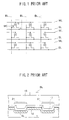
- FIG. 1 shows an array of NOR flash memory cells MC of a conventional non-volatile semiconductor memory device. It is indispensable for a method of manufacturing the non-volatile semiconductor memory device to scale down the NOR flash memory cells MC provided thereon.
- the NOR flash memory cells MC which are transistors, are arrayed such that the transistors in each row have sources S coupled to a common source line SL and gates G coupled to a common word line WL parallel to the common source line SL. Also, the transistors in each column have drains DR coupled to a common bit line BL.
- Such a source line SL may be used to perform flash-erasing or the like.
- FIG. 2 is a cross-sectional diagram showing a configuration of the conventional semiconductor memory device, taken along the source line SL of FIG. 1.
- reference numeral 1 denotes a silicon semiconductor substrate, 17 a CVD (Chemical Vapor Deposition) oxide film, 18 a BPSG (Boro-Phospho Silicate Glass) film, and 21 a field oxide film.
- CVD Chemical Vapor Deposition
- BPSG Bo-Phospho Silicate Glass
- the source line SL is formed such that the field oxide film 21 is formed on the silicon semiconductor substrate 1 by means of a LOCOS (local oxidation of silicon) element isolation process and is etched by means of a SAS (Self-Aligned Source) process after the gates G are formed, and a continuous impurity diffusion region including source diffusion regions 12 of the semiconductor memory cells MC (transistors) is formed as the source line SL on the silicon semiconductor substrate 1.
- LOCOS local oxidation of silicon
- SAS Self-Aligned Source
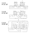
- FIG. 3 is a plan view partly showing a configuration of the conventional semiconductor memory device including the NOR flash memory cells MC.
- FIGS. 4A through 4D are diagrams partly showing a cross-sectional configuration of the conventional semiconductor memory device, taken along a word line WL A-A' in FIG. 3.
- a pad oxide film 2 with a thickness of approximately 25 nm is formed by means of a thermal oxidation process, which may be performed at 900°C for example.
- a silicon nitride film 3 with a thickness of approximately 170 nm is stacked by a Chemical Vapor Deposition (CVD) process.
- CVD Chemical Vapor Deposition
- the silicon semiconductor substrate 1 is thermally oxidized at approximately 1100°C by means of the silicon nitride film 3 serving as a mask, so that a LOCOS element isolation region 4 with a thickness of approximately 300 nm is formed.
- the silicon nitride film 3 and the pad oxide film 2 are removed so that a tunnel insulation film 5 with a thickness of approximately 10 nm is formed on the silicon semiconductor substrate 1 by means of the thermal oxidation process, which may be performed at 900°C for example.
- a polysilicon film 6 with a thickness of approximately 100 nm is stacked as a floating gate on the tunnel insulation film 5 by means of the CVD process.
- the polysilicon film 6 is patterned to form a striped pattern covering the element regions by means of the lithography and etching techniques.
- an ONO film 7 for combining capacitance of the floating gate and a control gate may be formed such that an oxide film with a thickness of approximately 10 nm is formed by means of the CVD process, a silicon nitride film with a thickness of approximately 10 nm is stacked on the an oxide film, and an oxide film with a thickness of approximately 4 nm is further stacked on the silicon nitride film by means of the thermal oxidation process which may be performed at 950°C for example.
- a polysilicon film 8 with a thickness of approximately 120 nm is formed as the control gate by means of the CVD process.
- a WSi film 9 with a thickness of approximately 150 nm is stacked.
- a polysilicon film 10 with a thickness of approximately 50 nm is stacked.
- a silicon nitride oxide film 11 with a thickness of approximately 100 nm is stacked, serving as an anti-reflection film at the time of resist patterning.
- FIGS. 5A through 5C are, on the other hand, diagrams partly showing a cross-sectional configuration of the conventional semiconductor memory device, taken along a bit line (aluminum wire) D-D' in FIG. 3.
- resist in a pattern extending in a direction intersecting a pattern of the LOCOS element isolation region 4 shown in FIG. 3 is applied thereon (not shown), and by using the resist as a mask, the silicon nitride oxide film 11, the polysilicon film 10, the WSi film 9, and the polysilicon film 8 are etched in order.
- the word line WL connected to the control gate of the semiconductor memory cell MC is thus formed.
- the ONO film 7 and the polysilicon film 6 are etched by using the silicon nitride oxide film 11 as a mask, and thereby a stacked gate electrode is formed.
- a self-aligned ion implantation for the stacked gate impurities are implanted into the silicon semiconductor substrate 1, and a thermal process is performed half an hour in a nitrogen atmosphere of, for example, approximately 900°C. Thereby, a source diffusion region 12 and a drain diffusion region 13 are formed.
- the above-mentioned ion implantation is performed such that, for example, AS + ions are accelerated with energy of 60 KeV and then are irradiated into the silicon semiconductor substrate 1 by a dose of 4 ⁇ 10 15 ions/cm 2 .
- a silicon oxide film 14 with a thickness of approximately 100 nm is stacked thereon by means of the CVD process and then is etched back. Thereby, the silicon oxide film 14 becomes a side wall spacer. After that, in order to expose the source diffusion region 12 by means of the lithography technique, the resist covering the drain diffusion region 13 is patterned and the LOCOS element isolation region 4 shown in FIG. 3 is etched.
- the silicon oxide film 17 with a thickness of approximately 100 nm and the BPSG film 18 with a thickness of approximately 900 nm are stacked thereon by means of the CVD process. After that, a contact hole 19 is formed, and an aluminum wiring film is stacked on the BPSG film 18 by using a spattering process. Then, the aluminum wiring film is patterned into the bit line BL.
- metal wiring is carried out, which is the same as that of a common MOS integrated circuit, and a surface protecting insulation film is formed. Accordingly, the semiconductor memory device is thus manufactured.
- FIG. 6 is a cross-sectional diagram showing a configuration of the semiconductor memory device, taken along a line B-B' in FIG. 3.
- the LOCOS element isolation region 4 and the drain diffusion region 13 are formed, and the silicon oxide film 17 and the BPSG film 18 are stacked thereon. After that, the contact hole 19 is opened, and the aluminum wiring film is formed as the bit line BL.
- FIG. 7 is a cross-sectional diagram showing a configuration of the semiconductor memory device, taken along a line E-E' in FIG. 3.
- the LOCOS element isolation region 4 and the source line SL are formed on the silicon semiconductor substrate 1.
- the polysilicon film 8, the WSi film 9, the polysilicon film 10, and the silicon nitride oxide film 11 are stacked on the LOCOS element isolation region 4 in order.
- the silicon oxide film 14 is formed as the side wall spacer. Further, the silicon oxide film 17 and the BPSG film 18 are stacked thereon in order.
- FIG. 8A is a cross-sectional diagram along a line C-C' of FIG. 3, showing the source line SL of the NOR-type flash memory manufactured by the conventional manufacturing method that makes use of the trench element isolation process.
- the trench element isolation process it is difficult for the trench element isolation process to form the source line SL.
- the source line SL can be easily formed by the ion implantation.
- parts Mt which are formed by etching the element isolation regions on the silicon semiconductor substrate 1 by means of the SAS process, have sharp steps, the impurities cannot be effectively introduced into the steps by means of anisotropic ion implantation, and the source line SL cannot be formed.
- the conventional manufacturing method cannot be used to manufacture the semiconductor memory device including the NOR-type flash memory cells in the case of employing the trench element isolation process.
- FIG. 8B is a cross-sectional diagram showing a non-volatile memory device formed by using the trench element isolation process, which is disclosed in Japanese Laid-open Patent Application No. 2-833030.
- a CVD tungsten layer is formed like a bridge built over n-type source diffusion regions of semiconductor memory cells. Since the element isolation regions and the n-type source diffusion regions are formed unevenly, there brings about a problem in that resistance of the CVD tungsten layer becomes high on the element isolation regions and the breaking thereof may occur in the most case.
- Another and a more specific object of the present invention is to provide a semiconductor memory device with high density and a method for manufacturing the semiconductor memory device including a plurality of semiconductor memory cells, sources of which are connected to source lines.
- a semiconductor memory device including a semiconductor substrate, a plurality of memory cells arranged on the semiconductor substrate in an array which is made up of a plurality of rows and columns, each of the memory cells having a gate, a drain, and a source, a plurality of word lines, each coupled to gates of the memory cells in a corresponding row, a plurality of bit lines, each coupled to drains of the memory cells in a corresponding column, a plurality of isolation regions formed on the semiconductor substrate and isolating the memory cells, and a plurality of source lines, disposed approximately parallel to the word lines, and each coupled to sources of the memory cells in a corresponding row, wherein each of the source lines is made up of a conductive pattern formed on an approximately flat region of the semiconductor substrate.
- a method for manufacturing a semiconductor memory device which includes an isolation region formed on a semiconductor substrate, source and drain diffusion regions formed in the semiconductor substrate, a gate oxide film formed on the semiconductor substrate between the source and drain diffusion regions, a floating gate formed on the gate oxide film, and a control gate formed on the floating gate via a first insulation film, the method comprising the steps of forming an second insulation film on an exposed portion of the substrate not covered by the isolation region and etching the second insulation film to expose the source diffusion regions, and forming a conductor on the exposed source diffusion region.
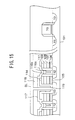
- FIG. 9 is a plan view showing a configuration of the semiconductor memory device of the first embodiment.
- the semiconductor memory device includes a silicon semiconductor substrate 101 (not shown), on which a plurality of NOR flash memory cells, a plurality of trench element isolation regions 104, a plurality of bit lines BL, and a plurality of word lines WL are arranged.
- the NOR flash memory cells are arranged on the silicon semiconductor substrate 101 in an array which is made up of a plurality of rows and columns, each of the memory cells having a gate G, a drain D R and source S.
- Each of the word lines WL is coupled to gates G of the memory cells in a corresponding row.
- Each of the bit lines BL is coupled to drains DR of the memory cells in a corresponding column.
- the trench element isolation regions 104 formed on the semiconductor substrate 101 such that they are parallel with each other and in predetermined intervals, serving to isolate the memory cells.
- the source lines SL are disposed approximately parallel to the word lines WL and are each coupled to sources S of the memory cells in a corresponding row.
- Each of the source lines SL is made up of a conductive pattern formed on an approximately flat region of the semiconductor substrate.
- bit lines BL are arranged in a direction in which the trench element isolation regions 104 are arranged.
- word lines WL are arranged in a direction approximately vertical to the trench element isolation regions 104 and the bit lines BL.
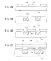
- FIGS. 10A through 10D are diagrams showing a cross-sectional configuration of the semiconductor memory device of the first embodiment, taken along a line A-A' of FIG. 9, the word line WL.
- a pad oxide film 102 with a thickness of approximately 25 nm is formed by means of a thermal oxidation process, which may be performed at 900°C for example.
- a silicon nitride film 103 with a thickness of approximately 170 nm is stacked by the Chemical Vapor Deposition (CVD) process.
- CVD Chemical Vapor Deposition
- the silicon semiconductor substrate 101 is etched to form a plurality of trenches thereon each with a depth of approximately 400 nm by using the silicon nitride film 103 as a mask.
- the etched trenches are filled with an oxide film having a thickness of approximately 1000 nm by means of the CVD process.
- the oxide film is buried into the etched trenches by employing a Chemical Mechanical Polish (CMP) process to polish a surface thereof, so that the trench element isolation regions 104 is formed.
- CMP Chemical Mechanical Polish
- a tunnel insulation film 105 with a thickness of approximately 10 nm is formed on the silicon semiconductor substrate 101 by means of the thermal oxidation process. And then, a polysilicon film 106 with a thickness of approximately 100 nm is stacked as a floating gate on the tunnel insulation film 105 by means of the CVD process. After that, the polysilicon film 106 is doped with phosphorus until resistivity thereof reaches to approximately 300 ⁇ /cm. In addition, at this time, an amorphous silicon film, which is doped by phosphorus, may be used instead of the polysilicon film 106.
- the polysilicon film 106 is patterned into a stripped pattern for covering element forming regions.
- an ONO film 107 for combining capacitance of the floating gate and a control gate may be formed such that an oxide film with a thickness of approximately 10 nm is formed by means of the CVD process, a silicon nitride film with a thickness of approximately 10 nm is stacked on the an oxide film, and an oxide film with a thickness of approximately 4 nm is further stacked on the silicon nitride film by means of the thermal oxidation process which may be performed at 950°C for example.
- a polysilicon film 108 with a thickness of approximately 120 nm is stacked as the control gate by means of the CVD process.
- the polysilicon film 108 is doped with the phosphorus until resistivity thereof reaches to approximately 60 ⁇ /cm.
- the amorphous silicon film, which is doped by phosphorus may be used instead of the polysilicon film 108.
- a WSi film 109 with a thickness of approximately 150 nm is stacked on the polysilicon film 108.
- a silicon nitride oxide film 111 with a thickness of approximately 100 nm is further stacked on the WSi film 109.
- the silicon nitride oxide film 111 serves as an anti-reflection film in exposure at the time of resist patterning.
- FIGS. 11A through 11C are cross-sectional diagrams showing a configuration of the semiconductor memory device of the first embodiment, taken along a line D-D' in the bit line BL of FIG. 9.
- resist (not shown) in a pattern extending in a direction intersecting a pattern of the trench element isolation region 104 shown in FIG. 9 is applied thereon. Then, the silicon nitride oxide film 111, the WSi film 109, and the polysilicon film 108 are etched in order by using the resist as a mask.
- the word line WL connected to the control gates of the semiconductor memory cells MC is thus formed.
- a stacked gate electrode is formed by using the silicon nitride oxide film 111 as a mask to etch the ONO film 107 and the polysilicon film 106.
- a self-aligned ion implantation for the stacked gate impurities are implanted into the silicon semiconductor substrate 101, and the thermal process is performed half an hour in a nitrogen atmosphere of, for example, approximately 900°C. Thereby, a source diffusion region 112 and a drain diffusion region 113 are thus formed.
- the above-mentioned ion implantation is performed such that, for example, AS + ions are accelerated with the energy of 60 KeV and then irradiated into the silicon semiconductor substrate 101 by a dose of 4 ⁇ 10 15 ions/cm 2 .
- a width of the drain diffusion region 113 in a direction along the trench element isolation region 104 is equal to or broader than that of the source diffusion region 112.
- a silicon oxide film 114 with a thickness of approximately 100 nm is stacked by means of the CVD process, and the source diffusion region 112 is exposed by means of the lithography technique. Therefore, resist 115 covering the drain diffusion region 113 is patterned.
- a nitride film may be stacked instead of the silicon oxide film 114.
- the silicon oxide film 114 is formed as a side wall spacer on the source diffusion region 112 by means of the self-aligned process.
- the silicon nitride oxide film 11 serves as an etching stopper.
- a conductive polysilicon film 116a with a thickness of approximately 120 nm and a conductive WSi film 116b with a thickness of approximately 15 nm are stacked on the source diffusion region 112. And then, by means of the lithography and etching techniques, the resist 115 is patterned and etched so that the source line SL can be formed as shown in FIG. 9. Since the side wall spacer formed by the silicon oxide film 114 serves as an insulation film, the word line WL and the source line SL are electrically insulated from each other.
- a metal film may be used instead of the polysilicon film 116a and the WSi film 116b.
- FIG. 12 is another diagram showing a cross-sectional configuration of the semiconductor memory device of the first embodiment, taken along the D-D' line of FIG. 9.
- a silicon oxide film 117 with a thickness of approximately 100 nm and a BPSG film 118 with a thickness of approximately 900 nm are stacked thereon by means of the CVD process. Then, resist (not shown) for forming a contact hole 119 is applied thereon and then is patterned and etched so that the contact hole 119 can be formed.
- FIG. 13 is a diagram showing a cross-sectional configuration of the semiconductor memory device of the first embodiment, taken along a line B-B' of FIG. 9.
- the trench element isolation region 104 and the drain diffusion region 113 are stacked on the silicon semiconductor substrate 101.
- the silicon oxide films 114, 117 and the BPSG film 118 are further stacked on the trench element isolation region 104 and the drain diffusion region 112. After that, the contact hole 119 is opened, and thereby the aluminum wiring film is formed as the bit line BL.
- FIG. 14 is a diagram showing a cross-sectional configuration of the semiconductor memory device of the first embodiment, taken along a line C-C' of FIG. 9.
- the trench element isolation region 104 and the source diffusion region 112 are flat formed on the silicon semiconductor substrate 101.
- the polysilicon film 116a and the WSi film 116b are stacked on the trench element isolation region 104 and the source diffusion region 112. Further, the silicon oxide film 117 and the BPSG film 118 are stacked on the WSi film 116b.
- the bit line BL is formed.
- the metal wiring is performed, which is the same as that of the common MOS integrated circuit, and then a surface protecting insulation film is formed thereon.
- the semiconductor memory device of the first embodiment is manufactured.
- the pad oxide film 102 with a thickness of approximately 25 nm is formed by means of the thermal oxidation process performed at, for example, 900°C.
- the silicon nitride film 103 with a thickness of approximately 170 nm is stacked by means of the Chemical Vapor Deposition (CVD) process.
- CVD Chemical Vapor Deposition
- the silicon nitride film 103 is patterned and etched so as to remain on element regions alone.
- the silicon semiconductor substrate 101 is etched to form a plurality of trenches with a depth of approximately 400 nm by means of the silicon nitride film 103 used as a mask, and the etched trenches are stacked with an oxide film having a thickness of approximately 1000 nm by means of the CVD process. Then, the oxide film has its surface polished by means of the Chemical Mechanical Polish (CMP) process so as to be buried in the etched trenches to form the trench element isolation regions 104. After that, the silicon nitride film 103 and the pad oxide film 102 are removed therefrom.
- CMP Chemical Mechanical Polish
- the tunnel insulation film 105 with a thickness of approximately 10 nm is formed on the silicon semiconductor substrate 101 by means of the thermal oxidation process.
- the polysilicon film 106 with a thickness of approximately 100 nm is stacked as a floating gate on the tunnel insulation film 105 by means of the CVD process.
- the polysilicon film 106 is doped with the phosphorus until resistivity thereof reaches to approximately 300 ⁇ /cm.
- the amorphous silicon film which is phosphorus-doped, may be used instead of the polysilicon film 106.
- the polysilicon film 106 is patterned into a stripped pattern so as to cover the element forming regions.
- the ONO film 107 for combining capacitance of the floating gate and the control gate may be formed such that an oxide film with a thickness of approximately 10 nm is formed by means of the CVD process, the silicon nitride film with a thickness of approximately 10 nm is stacked on the an oxide film, and the oxide film with a thickness of approximately 4 nm is further stacked on the silicon nitride film by means of the thermal oxidation process performed at, for example, 950°C.
- the polysilicon film 108 with a thickness of approximately 120 nm is stacked thereon as the control gate by means of the CVD process.
- the polysilicon film 108 is doped with the phosphorus until resistivity thereof reaches to approximately 60 ⁇ /cm.
- the amorphous silicon film which is phosphorus-doped may be used instead of the polysilicon film 108.
- the WSi film 109 with a thickness of approximately 150 nm is formed. And on the WSi film 109, the silicon nitride oxide film 111 with a thickness of approximately 100 nm is formed.
- the silicon nitride oxide film 111 serves as the anti-reflection film in exposure at the time of the resist patterning.
- FIGS. 16A through 16C are, on the other hand, cross-sectional diagrams showing a configuration of the semiconductor memory device of the second embodiment, taken along the line D-D' in FIG. 9.
- resist (not shown) in a pattern extending in a direction intersecting a pattern of the trench element isolation region 104 shown in FIG. 9 is applied thereon.
- the resist is used as a mask so that the silicon nitride oxide film 111, the WSi film 109, and the polysilicon film 108 are etched in order.
- the word line WL connected to the control gate of the semiconductor memory cell MC is thus formed.
- the ONO film 107 and the polysilicon film 106 are etched by means of the silicon nitride oxide film 111 used as a mask so that the stacked gate electrode is formed.
- the above-mentioned ion implantation is performed such that, for example, AS + ions are accelerated with the energy of 60 KeV and then are irradiated into the silicon semiconductor substrate 101 by a dose of 4 ⁇ 10 15 ions/cm 2 .
- the width of the drain diffusion region 113 in the direction along the trench element isolation region 104 is equal to or broader than that of the source diffusion region 112.
- the resist 115 is patterned so as to expose the source diffusion region 112 by means of the lithography technique and to form the contact hole 119 on the drain diffusion region 113.
- a nitride film may be stacked instead of the silicon oxide film 114.
- the silicon oxide film 114 is formed as a side wall spacer on the source diffusion region 112 by means of the self-aligned process, and the contact hole 119 is formed on the drain diffusion region 113.
- the silicon nitride oxide film 11 serves as the etching stopper.
- a titanium film 120 with a thickness of about 30 nm, a nitride titanium film 121 with a thickness of about 50 nm, and a tungsten layer 122 with a thickness of approximately 400 nm are stacked on both the source diffusion region 112 and the drain diffusion region 113.
- the resist is patterned and the stacked films are etched so that the source line SL is formed and the plug is buried on the drain diffusion region 113. Then, since the side wall spacer formed from the silicon oxide film 114 is the insulation film, the word line WL and the source line SL are electrically insulated from each other.
- the silicon oxide film 117 with a thickness of about 100 nm and the BPSG film 118 with a thickness of about 900 nm are stacked thereon by means of the CVD process.
- the resist (not shown) used for forming the contact hole 119 is patterned and the above-mentioned films are etched so that the contact hole 119 can be formed as shown in FIG. 17.
- the aluminum films are stacked by using the spattering process and patterned so that the bit line BL is formed.
- the metal wiring is performed in the same way as that on the common MOS integrated circuit, and then the surface protecting insulation film is formed. Finally, the semiconductor memory device of the second embodiment is thus manufactured.
- the above-mentioned silicon semiconductor substrate 101 may be the SOI semiconductor substrate.
- the semiconductor memory device can operate with higher speed because parasitic capacitance is reduced.
- FIG. 18 is another diagram showing a cross-sectional configuration of the semiconductor memory device of the second embodiment in a case of using the SOI semiconductor substrate, taken along the line D-D' of FIG. 9.
- FIG. 15 is a diagram showing a cross-sectional configuration of the semiconductor memory device in accordance with the present invention. As shown in this diagram, the NOR flash memory cell in accordance with the present invention is provided on the silicon semiconductor substrate 101, as well as a transistor including a gate TG, a source diffusion region TS and a drain diffusion region TD.
- the NOR flash memory can be easily manufactured even in the case of employing the trench element isolation process.
- the semiconductor memory device including the NOR flash memory cells with high density can be obtained by the method of the present invention.
Abstract
Description
- This application is based upon and claims priority of Japanese Patent Application No. 11-215601 filed on July 29, 1999, the contents being incorporated herein by reference.
- The present invention generally relates to semiconductor memory devices and methods for manufacturing the same, and more particularly to a semiconductor memory device including a plurality of semiconductor memory cells, sources of which are coupled to source lines, and a method for manufacturing such a semiconductor memory device.
- FIG. 1 shows an array of NOR flash memory cells MC of a conventional non-volatile semiconductor memory device. It is indispensable for a method of manufacturing the non-volatile semiconductor memory device to scale down the NOR flash memory cells MC provided thereon.
- As shown in FIG. 1, the NOR flash memory cells MC, which are transistors, are arrayed such that the transistors in each row have sources S coupled to a common source line SL and gates G coupled to a common word line WL parallel to the common source line SL. Also, the transistors in each column have drains DR coupled to a common bit line BL.
- In addition, such a source line SL may be used to perform flash-erasing or the like.
- FIG. 2 is a cross-sectional diagram showing a configuration of the conventional semiconductor memory device, taken along the source line SL of FIG. 1. In this diagram,
reference numeral 1 denotes a silicon semiconductor substrate, 17 a CVD (Chemical Vapor Deposition) oxide film, 18 a BPSG (Boro-Phospho Silicate Glass) film, and 21 a field oxide film. - As shown in FIG. 2, in order to scale down the semiconductor memory cells MC provided on the
semiconductor substrate 1, the source line SL is formed such that thefield oxide film 21 is formed on thesilicon semiconductor substrate 1 by means of a LOCOS (local oxidation of silicon) element isolation process and is etched by means of a SAS (Self-Aligned Source) process after the gates G are formed, and a continuous impurity diffusion region includingsource diffusion regions 12 of the semiconductor memory cells MC (transistors) is formed as the source line SL on thesilicon semiconductor substrate 1. - Next, a description will be given below of a method of using the SAS process to manufacture the NOR flash memory cells MC, by referring to FIG. 3 through FIG. 7.
- FIG. 3 is a plan view partly showing a configuration of the conventional semiconductor memory device including the NOR flash memory cells MC.
- FIGS. 4A through 4D are diagrams partly showing a cross-sectional configuration of the conventional semiconductor memory device, taken along a word line WL A-A' in FIG. 3.
- As shown in FIG. 4A, on the
silicon semiconductor substrate 1, apad oxide film 2 with a thickness of approximately 25 nm is formed by means of a thermal oxidation process, which may be performed at 900°C for example. On thepad oxide film 2, asilicon nitride film 3 with a thickness of approximately 170 nm is stacked by a Chemical Vapor Deposition (CVD) process. And then, by using lithography and etching techniques, thesilicon nitride film 3 is patterned and etched so as to remain on element regions alone. - As shown in FIG. 4B, the
silicon semiconductor substrate 1 is thermally oxidized at approximately 1100°C by means of thesilicon nitride film 3 serving as a mask, so that a LOCOSelement isolation region 4 with a thickness of approximately 300 nm is formed. - As shown in FIG. 4C, the
silicon nitride film 3 and thepad oxide film 2 are removed so that atunnel insulation film 5 with a thickness of approximately 10 nm is formed on thesilicon semiconductor substrate 1 by means of the thermal oxidation process, which may be performed at 900°C for example. After that, apolysilicon film 6 with a thickness of approximately 100 nm is stacked as a floating gate on thetunnel insulation film 5 by means of the CVD process. And then, thepolysilicon film 6 is patterned to form a striped pattern covering the element regions by means of the lithography and etching techniques. - As shown in FIG. 4D, an
ONO film 7 for combining capacitance of the floating gate and a control gate may be formed such that an oxide film with a thickness of approximately 10 nm is formed by means of the CVD process, a silicon nitride film with a thickness of approximately 10 nm is stacked on the an oxide film, and an oxide film with a thickness of approximately 4 nm is further stacked on the silicon nitride film by means of the thermal oxidation process which may be performed at 950°C for example. - After that, a
polysilicon film 8 with a thickness of approximately 120 nm is formed as the control gate by means of the CVD process. On thepolysilicon film 8, aWSi film 9 with a thickness of approximately 150 nm is stacked. And further on the WSifilm 9, apolysilicon film 10 with a thickness of approximately 50 nm is stacked. Furthermore, on thepolysilicon film 10, a siliconnitride oxide film 11 with a thickness of approximately 100 nm is stacked, serving as an anti-reflection film at the time of resist patterning. - FIGS. 5A through 5C are, on the other hand, diagrams partly showing a cross-sectional configuration of the conventional semiconductor memory device, taken along a bit line (aluminum wire) D-D' in FIG. 3.
- As shown in FIG. 5A, resist in a pattern extending in a direction intersecting a pattern of the LOCOS
element isolation region 4 shown in FIG. 3 is applied thereon (not shown), and by using the resist as a mask, the siliconnitride oxide film 11, thepolysilicon film 10, theWSi film 9, and thepolysilicon film 8 are etched in order. - Thereby, the word line WL connected to the control gate of the semiconductor memory cell MC is thus formed. After that, the ONO
film 7 and thepolysilicon film 6 are etched by using the siliconnitride oxide film 11 as a mask, and thereby a stacked gate electrode is formed. - Then, by performing a self-aligned ion implantation for the stacked gate, impurities are implanted into the
silicon semiconductor substrate 1, and a thermal process is performed half an hour in a nitrogen atmosphere of, for example, approximately 900°C. Thereby, asource diffusion region 12 and adrain diffusion region 13 are formed. In addition, the above-mentioned ion implantation is performed such that, for example, AS+ ions are accelerated with energy of 60 KeV and then are irradiated into thesilicon semiconductor substrate 1 by a dose of 4 × 10¹⁵ ions/cm2. - As shown in FIG. 5B, a
silicon oxide film 14 with a thickness of approximately 100 nm is stacked thereon by means of the CVD process and then is etched back. Thereby, thesilicon oxide film 14 becomes a side wall spacer. After that, in order to expose thesource diffusion region 12 by means of the lithography technique, the resist covering thedrain diffusion region 13 is patterned and the LOCOSelement isolation region 4 shown in FIG. 3 is etched. - Then, By implanting the As+ ions, which have been accelerated with the energy of 60 KeV, thereinto by a dose of 4 × 10¹⁵ ions/cm2, and by performing the thermal process half an hour in the nitrogen atmosphere of, for example, 850°C, a continuous diffusion region connecting the
source diffusion regions 12 of the semiconductor memory cells MC is formed as the source line SL. - As shown in FIG. 5C, the
silicon oxide film 17 with a thickness of approximately 100 nm and theBPSG film 18 with a thickness of approximately 900 nm are stacked thereon by means of the CVD process. After that, acontact hole 19 is formed, and an aluminum wiring film is stacked on the BPSGfilm 18 by using a spattering process. Then, the aluminum wiring film is patterned into the bit line BL. - After the previously described steps are completed, metal wiring is carried out, which is the same as that of a common MOS integrated circuit, and a surface protecting insulation film is formed. Accordingly, the semiconductor memory device is thus manufactured.
- FIG. 6 is a cross-sectional diagram showing a configuration of the semiconductor memory device, taken along a line B-B' in FIG. 3.
- As shown in this diagram, on the
silicon semiconductor substrate 1, the LOCOSelement isolation region 4 and thedrain diffusion region 13 are formed, and thesilicon oxide film 17 and theBPSG film 18 are stacked thereon. After that, thecontact hole 19 is opened, and the aluminum wiring film is formed as the bit line BL. - FIG. 7 is a cross-sectional diagram showing a configuration of the semiconductor memory device, taken along a line E-E' in FIG. 3.
- As shown in this diagram, the LOCOS
element isolation region 4 and the source line SL are formed on thesilicon semiconductor substrate 1. Thepolysilicon film 8, the WSifilm 9, thepolysilicon film 10, and the siliconnitride oxide film 11 are stacked on the LOCOSelement isolation region 4 in order. And thesilicon oxide film 14 is formed as the side wall spacer. Further, thesilicon oxide film 17 and the BPSGfilm 18 are stacked thereon in order. - There is, however, a limitation in the LOCOS element isolation process in terms of scaling down the element isolation regions. In recent years, a trench element isolation process performed by etching a semiconductor semiconductor substrate has been become popular, which is required to be able to form elements the same as those formed by the LOCOS element isolation process.
- FIG. 8A is a cross-sectional diagram along a line C-C' of FIG. 3, showing the source line SL of the NOR-type flash memory manufactured by the conventional manufacturing method that makes use of the trench element isolation process.
- As shown in FIG. 8A, it is difficult for the trench element isolation process to form the source line SL. Specifically, in the case of employing the LOCOS element isolation process shown by FIG. 2, since
parts 21 formed by etching element isolation regions on thesilicon semiconductor substrate 1 have gently inclined surfaces, the source line SL can be easily formed by the ion implantation. On the other hand, in the case of employing the trench element isolation process, since parts Mt, which are formed by etching the element isolation regions on thesilicon semiconductor substrate 1 by means of the SAS process, have sharp steps, the impurities cannot be effectively introduced into the steps by means of anisotropic ion implantation, and the source line SL cannot be formed. - As a result, the conventional manufacturing method cannot be used to manufacture the semiconductor memory device including the NOR-type flash memory cells in the case of employing the trench element isolation process.
- FIG. 8B is a cross-sectional diagram showing a non-volatile memory device formed by using the trench element isolation process, which is disclosed in Japanese Laid-open Patent Application No. 2-833030.
- As shown in this diagram, a CVD tungsten layer is formed like a bridge built over n-type source diffusion regions of semiconductor memory cells. Since the element isolation regions and the n-type source diffusion regions are formed unevenly, there brings about a problem in that resistance of the CVD tungsten layer becomes high on the element isolation regions and the breaking thereof may occur in the most case.
- As a result, it is difficult to form the source line SL with high-reliability and low-resistance by means of the above-mentioned prior art.
- It is a general object of the present invention to provide a semiconductor memory device and a method for manufacturing the same, in which the above-mentioned problems can be eliminated.
- Another and a more specific object of the present invention is to provide a semiconductor memory device with high density and a method for manufacturing the semiconductor memory device including a plurality of semiconductor memory cells, sources of which are connected to source lines.
- The above object and other objects of the present invention are achieved by a semiconductor memory device including a semiconductor substrate, a plurality of memory cells arranged on the semiconductor substrate in an array which is made up of a plurality of rows and columns, each of the memory cells having a gate, a drain, and a source, a plurality of word lines, each coupled to gates of the memory cells in a corresponding row, a plurality of bit lines, each coupled to drains of the memory cells in a corresponding column, a plurality of isolation regions formed on the semiconductor substrate and isolating the memory cells, and a plurality of source lines, disposed approximately parallel to the word lines, and each coupled to sources of the memory cells in a corresponding row, wherein each of the source lines is made up of a conductive pattern formed on an approximately flat region of the semiconductor substrate.
- The above object and other objects of the present invention are achieved by a method for manufacturing a semiconductor memory device which includes an isolation region formed on a semiconductor substrate, source and drain diffusion regions formed in the semiconductor substrate, a gate oxide film formed on the semiconductor substrate between the source and drain diffusion regions, a floating gate formed on the gate oxide film, and a control gate formed on the floating gate via a first insulation film, the method comprising the steps of forming an second insulation film on an exposed portion of the substrate not covered by the isolation region and etching the second insulation film to expose the source diffusion regions, and forming a conductor on the exposed source diffusion region.
- Other objects, features and advantages of the present invention will become more apparent from the following detailed description when read in conjunction with the accompanying drawings.
-
- FIG. 1 is a diagram showing an array of NOR flash memory cells of a conventional non-volatile semiconductor memory device;
- FIG. 2 is a cross-sectional diagram showing a configuration of the conventional semiconductor memory device, taken along a source line SL of FIG. 1;
- FIG. 3 is a plan view showing a configuration of the conventional semiconductor memory device having the NOR flash memory cells;
- FIGS. 4A through 4D are diagrams partly showing a cross-sectional configuration of the conventional semiconductor memory device, taken along a line A-A' of FIG. 3;
- FIGS. 5A through 5C are diagrams partly showing a cross-sectional configuration of the conventional semiconductor memory device, taken along a line D-D' of FIG. 3;
- FIG. 6 is a diagram showing a cross-sectional configuration of the conventional semiconductor memory device, taken along a line B-B' of FIG. 3;
- FIG. 7 is a diagram showing a cross-sectional configuration of the conventional semiconductor memory device, taken along a line E-E' of FIG. 3;
- FIG. 8A is a cross-sectional diagram showing a source line of the NOR flash memory cells, which is formed by using a trench element isolation process and a conventional manufacturing method, and FIG. 8B is a cross-sectional diagram showing a semiconductor memory device disclosed in Japanese Laid-open Patent Application No. 2-833030;
- FIG. 9 is a plan view showing a configuration of a semiconductor memory device including NOR flash memory cells according to a first embodiment of the present invention;
- FIGS. 10A through 10D are diagrams showing a cross-sectional configuration of the semiconductor memory device of the first embodiment, taken along a line A-A' of FIG. 9;
- FIGS. 11A through 11C are diagrams showing a cross-sectional configuration of the semiconductor memory device of the first embodiment, taken along a line D-D' of FIG. 9;
- FIG. 12 is another diagram showing a cross-sectional configuration of the semiconductor memory device of the first embodiment, taken along the line D-D' of FIG. 9;
- FIG. 13 is a diagram showing a cross-sectional configuration of the semiconductor memory device of the first embodiment, taken along a line B-B' of FIG. 9;
- FIG. 14 is a diagram showing a cross-sectional configuration of the semiconductor memory device of the first embodiment, taken along a line C-C' of FIG. 9;
- FIG. 15 is a diagram showing a cross-sectional configuration of the semiconductor memory device of the first embodiment, in a case where a transistor and the NOR flash memory cells are formed on one silicon semiconductor substrate thereof;
- FIGS. 16A through 16C are diagrams showing a cross-sectional configuration of the semiconductor memory device of a second embodiment, taken along the line D-D' of FIG. 9;
- FIG. 17 is another diagram showing a cross-sectional configuration of the semiconductor memory device of the second embodiment, taken along the line D-D' of FIG. 9; and
- FIG. 18 is another diagram showing a cross-sectional configuration of the semiconductor memory device of the second embodiment in a case of using a SOI (silicon on insulator) semiconductor substrate, taken along the line D-D' of FIG. 9.
-
- With reference to the drawings, a description will be given below of preferred embodiments of the present invention.
- First, a description will be given of a semiconductor memory device according to a first embodiment of the present invention, by referring to FIG. 9.
- FIG. 9 is a plan view showing a configuration of the semiconductor memory device of the first embodiment. As shown in this diagram, the semiconductor memory device includes a silicon semiconductor substrate 101 (not shown), on which a plurality of NOR flash memory cells, a plurality of trench
element isolation regions 104, a plurality of bit lines BL, and a plurality of word lines WL are arranged. - The NOR flash memory cells are arranged on the
silicon semiconductor substrate 101 in an array which is made up of a plurality of rows and columns, each of the memory cells having a gate G, a drain DR and source S. - Each of the word lines WL is coupled to gates G of the memory cells in a corresponding row. Each of the bit lines BL is coupled to drains DR of the memory cells in a corresponding column. The trench
element isolation regions 104 formed on thesemiconductor substrate 101 such that they are parallel with each other and in predetermined intervals, serving to isolate the memory cells. The source lines SL are disposed approximately parallel to the word lines WL and are each coupled to sources S of the memory cells in a corresponding row. Each of the source lines SL is made up of a conductive pattern formed on an approximately flat region of the semiconductor substrate. - Also, the bit lines BL are arranged in a direction in which the trench
element isolation regions 104 are arranged. The word lines WL are arranged in a direction approximately vertical to the trenchelement isolation regions 104 and the bit lines BL. - FIGS. 10A through 10D are diagrams showing a cross-sectional configuration of the semiconductor memory device of the first embodiment, taken along a line A-A' of FIG. 9, the word line WL.
- As shown in FIG. 10A, on the
silicon semiconductor substrate 101, apad oxide film 102 with a thickness of approximately 25 nm is formed by means of a thermal oxidation process, which may be performed at 900°C for example. On thepad oxide film 102, asilicon nitride film 103 with a thickness of approximately 170 nm is stacked by the Chemical Vapor Deposition (CVD) process. And then, by using the lithography and etching techniques, thesilicon nitride film 103 is patterned and etched so as to remain on element regions alone. - As shown in FIG. 10B, the
silicon semiconductor substrate 101 is etched to form a plurality of trenches thereon each with a depth of approximately 400 nm by using thesilicon nitride film 103 as a mask. The etched trenches are filled with an oxide film having a thickness of approximately 1000 nm by means of the CVD process. And then, the oxide film is buried into the etched trenches by employing a Chemical Mechanical Polish (CMP) process to polish a surface thereof, so that the trenchelement isolation regions 104 is formed. After that, thesilicon nitride film 103 and thepad oxide film 102 are removed therefrom. - As shown in FIG. 10C, a
tunnel insulation film 105 with a thickness of approximately 10 nm is formed on thesilicon semiconductor substrate 101 by means of the thermal oxidation process. And then, apolysilicon film 106 with a thickness of approximately 100 nm is stacked as a floating gate on thetunnel insulation film 105 by means of the CVD process. After that, thepolysilicon film 106 is doped with phosphorus until resistivity thereof reaches to approximately 300Ω/cm. In addition, at this time, an amorphous silicon film, which is doped by phosphorus, may be used instead of thepolysilicon film 106. - Next, by means of the lithography and etching techniques, the
polysilicon film 106 is patterned into a stripped pattern for covering element forming regions. - As shown in FIG. 10D, an
ONO film 107 for combining capacitance of the floating gate and a control gate may be formed such that an oxide film with a thickness of approximately 10 nm is formed by means of the CVD process, a silicon nitride film with a thickness of approximately 10 nm is stacked on the an oxide film, and an oxide film with a thickness of approximately 4 nm is further stacked on the silicon nitride film by means of the thermal oxidation process which may be performed at 950°C for example. - After that, on the
ONO film 107, apolysilicon film 108 with a thickness of approximately 120 nm is stacked as the control gate by means of the CVD process. Thepolysilicon film 108 is doped with the phosphorus until resistivity thereof reaches to approximately 60 Ω/cm. In addition, at this time, the amorphous silicon film, which is doped by phosphorus, may be used instead of thepolysilicon film 108. - On the
polysilicon film 108, aWSi film 109 with a thickness of approximately 150 nm is stacked. And on theWSi film 109, a siliconnitride oxide film 111 with a thickness of approximately 100 nm is further stacked. The siliconnitride oxide film 111 serves as an anti-reflection film in exposure at the time of resist patterning. - FIGS. 11A through 11C, on the other hand, are cross-sectional diagrams showing a configuration of the semiconductor memory device of the first embodiment, taken along a line D-D' in the bit line BL of FIG. 9.
- As shown in FIG. 11A, resist (not shown) in a pattern extending in a direction intersecting a pattern of the trench
element isolation region 104 shown in FIG. 9 is applied thereon. Then, the siliconnitride oxide film 111, theWSi film 109, and thepolysilicon film 108 are etched in order by using the resist as a mask. - Thereby, the word line WL connected to the control gates of the semiconductor memory cells MC is thus formed. After that, a stacked gate electrode is formed by using the silicon
nitride oxide film 111 as a mask to etch theONO film 107 and thepolysilicon film 106. - Then, by performing a self-aligned ion implantation for the stacked gate, impurities are implanted into the
silicon semiconductor substrate 101, and the thermal process is performed half an hour in a nitrogen atmosphere of, for example, approximately 900°C. Thereby, asource diffusion region 112 and adrain diffusion region 113 are thus formed. In addition, the above-mentioned ion implantation is performed such that, for example, AS+ ions are accelerated with the energy of 60 KeV and then irradiated into thesilicon semiconductor substrate 101 by a dose of 4 × 10¹⁵ ions/cm2. - It should be noted that a width of the
drain diffusion region 113 in a direction along the trenchelement isolation region 104 is equal to or broader than that of thesource diffusion region 112. - Then, on the silicon
nitride oxide film 11, asilicon oxide film 114 with a thickness of approximately 100 nm is stacked by means of the CVD process, and thesource diffusion region 112 is exposed by means of the lithography technique. Therefore, resist 115 covering thedrain diffusion region 113 is patterned. In addition, it can be also considered that a nitride film may be stacked instead of thesilicon oxide film 114. - As shown in FIG. 11B, by performing anisotropy etching and removing the resist 115, the
silicon oxide film 114 is formed as a side wall spacer on thesource diffusion region 112 by means of the self-aligned process. In addition, at this time, the siliconnitride oxide film 11 serves as an etching stopper. - As shown in FIG. 11C, a
conductive polysilicon film 116a with a thickness of approximately 120 nm and aconductive WSi film 116b with a thickness of approximately 15 nm are stacked on thesource diffusion region 112. And then, by means of the lithography and etching techniques, the resist 115 is patterned and etched so that the source line SL can be formed as shown in FIG. 9. Since the side wall spacer formed by thesilicon oxide film 114 serves as an insulation film, the word line WL and the source line SL are electrically insulated from each other. - In addition, it goes without saying that a metal film may be used instead of the
polysilicon film 116a and theWSi film 116b. - FIG. 12 is another diagram showing a cross-sectional configuration of the semiconductor memory device of the first embodiment, taken along the D-D' line of FIG. 9.
- As shown in this diagram, a
silicon oxide film 117 with a thickness of approximately 100 nm and aBPSG film 118 with a thickness of approximately 900 nm are stacked thereon by means of the CVD process. Then, resist (not shown) for forming acontact hole 119 is applied thereon and then is patterned and etched so that thecontact hole 119 can be formed. - After that, aluminum films are stacked thereon by means of a spattering process and is patterned into the bit line BL.
- FIG. 13 is a diagram showing a cross-sectional configuration of the semiconductor memory device of the first embodiment, taken along a line B-B' of FIG. 9.
- As shown in this diagram, the trench
element isolation region 104 and thedrain diffusion region 113 are stacked on thesilicon semiconductor substrate 101. Thesilicon oxide films BPSG film 118 are further stacked on the trenchelement isolation region 104 and thedrain diffusion region 112. After that, thecontact hole 119 is opened, and thereby the aluminum wiring film is formed as the bit line BL. - FIG. 14 is a diagram showing a cross-sectional configuration of the semiconductor memory device of the first embodiment, taken along a line C-C' of FIG. 9.
- As shown in this diagram, the trench
element isolation region 104 and thesource diffusion region 112 are flat formed on thesilicon semiconductor substrate 101. Thepolysilicon film 116a and theWSi film 116b are stacked on the trenchelement isolation region 104 and thesource diffusion region 112. Further, thesilicon oxide film 117 and theBPSG film 118 are stacked on theWSi film 116b. Thus, the bit line BL is formed. - In addition, after the above described processes are completed, the metal wiring is performed, which is the same as that of the common MOS integrated circuit, and then a surface protecting insulation film is formed thereon. Thus, the semiconductor memory device of the first embodiment is manufactured.
- Next, a description will be given below of a semiconductor memory device according to a second embodiment of the present invention, by referring to FIGS. 10A through 10D, FIG. 16 and FIG. 17.
- As shown in FIG. 10A, on the
silicon semiconductor substrate 101, thepad oxide film 102 with a thickness of approximately 25 nm is formed by means of the thermal oxidation process performed at, for example, 900°C. On thepad oxide film 102, thesilicon nitride film 103 with a thickness of approximately 170 nm is stacked by means of the Chemical Vapor Deposition (CVD) process. And then, by using lithography and etching techniques, thesilicon nitride film 103 is patterned and etched so as to remain on element regions alone. - As shown in FIG. 10B, the
silicon semiconductor substrate 101 is etched to form a plurality of trenches with a depth of approximately 400 nm by means of thesilicon nitride film 103 used as a mask, and the etched trenches are stacked with an oxide film having a thickness of approximately 1000 nm by means of the CVD process. Then, the oxide film has its surface polished by means of the Chemical Mechanical Polish (CMP) process so as to be buried in the etched trenches to form the trenchelement isolation regions 104. After that, thesilicon nitride film 103 and thepad oxide film 102 are removed therefrom. - As shown in FIG. 10C, the
tunnel insulation film 105 with a thickness of approximately 10 nm is formed on thesilicon semiconductor substrate 101 by means of the thermal oxidation process. After that, thepolysilicon film 106 with a thickness of approximately 100 nm is stacked as a floating gate on thetunnel insulation film 105 by means of the CVD process. And then, thepolysilicon film 106 is doped with the phosphorus until resistivity thereof reaches to approximately 300 Ω/cm. In addition, at this time, the amorphous silicon film, which is phosphorus-doped, may be used instead of thepolysilicon film 106. - Next, by employing the lithography and etching techniques, the
polysilicon film 106 is patterned into a stripped pattern so as to cover the element forming regions. - As shown in FIG. 10D, the
ONO film 107 for combining capacitance of the floating gate and the control gate may be formed such that an oxide film with a thickness of approximately 10 nm is formed by means of the CVD process, the silicon nitride film with a thickness of approximately 10 nm is stacked on the an oxide film, and the oxide film with a thickness of approximately 4 nm is further stacked on the silicon nitride film by means of the thermal oxidation process performed at, for example, 950°C. - After that, the
polysilicon film 108 with a thickness of approximately 120 nm is stacked thereon as the control gate by means of the CVD process. Thepolysilicon film 108 is doped with the phosphorus until resistivity thereof reaches to approximately 60Ω/cm. In addition, at this time, the amorphous silicon film which is phosphorus-doped may be used instead of thepolysilicon film 108. - On the
polysilicon film 108, theWSi film 109 with a thickness of approximately 150 nm is formed. And on theWSi film 109, the siliconnitride oxide film 111 with a thickness of approximately 100 nm is formed. The siliconnitride oxide film 111 serves as the anti-reflection film in exposure at the time of the resist patterning. - FIGS. 16A through 16C are, on the other hand, cross-sectional diagrams showing a configuration of the semiconductor memory device of the second embodiment, taken along the line D-D' in FIG. 9.
- As shown in FIG. 16A, resist (not shown) in a pattern extending in a direction intersecting a pattern of the trench
element isolation region 104 shown in FIG. 9 is applied thereon. The resist is used as a mask so that the siliconnitride oxide film 111, theWSi film 109, and thepolysilicon film 108 are etched in order. - Thereby, the word line WL connected to the control gate of the semiconductor memory cell MC is thus formed. After that, the
ONO film 107 and thepolysilicon film 106 are etched by means of the siliconnitride oxide film 111 used as a mask so that the stacked gate electrode is formed. - Then, by performing the self-aligned ion implantation for the stacked gate, impurities are implanted into the
silicon semiconductor substrate 101, and the thermal process is performed half an hour in the nitrogen atmosphere of, for example, approximately 900°C. Thereby, thesource diffusion region 112 and thedrain diffusion region 113 are formed. - In addition, the above-mentioned ion implantation is performed such that, for example, AS+ ions are accelerated with the energy of 60 KeV and then are irradiated into the
silicon semiconductor substrate 101 by a dose of 4 × 10¹⁵ ions/cm2. - Also, It should be noted that the width of the
drain diffusion region 113 in the direction along the trenchelement isolation region 104 is equal to or broader than that of thesource diffusion region 112. - After the
silicon oxide film 114 with a thickness of approximately 100 nm is stacked by means of the CVD process, the resist 115 is patterned so as to expose thesource diffusion region 112 by means of the lithography technique and to form thecontact hole 119 on thedrain diffusion region 113. - In addition, it is also considered that a nitride film may be stacked instead of the
silicon oxide film 114. - As shown in FIG. 16B, by performing the etching process and removing the resist 115, the
silicon oxide film 114 is formed as a side wall spacer on thesource diffusion region 112 by means of the self-aligned process, and thecontact hole 119 is formed on thedrain diffusion region 113. - In addition, at this time, the silicon
nitride oxide film 11 serves as the etching stopper. - As shown in FIG. 16C, for example, a titanium film 120 with a thickness of about 30 nm, a nitride titanium film 121 with a thickness of about 50 nm, and a tungsten layer 122 with a thickness of approximately 400 nm are stacked on both the
source diffusion region 112 and thedrain diffusion region 113. - And then, by using the lithography and etching techniques, the resist is patterned and the stacked films are etched so that the source line SL is formed and the plug is buried on the
drain diffusion region 113. Then, since the side wall spacer formed from thesilicon oxide film 114 is the insulation film, the word line WL and the source line SL are electrically insulated from each other. - Furthermore, as shown in FIG. 17, the
silicon oxide film 117 with a thickness of about 100 nm and theBPSG film 118 with a thickness of about 900 nm are stacked thereon by means of the CVD process. After that, the resist (not shown) used for forming thecontact hole 119 is patterned and the above-mentioned films are etched so that thecontact hole 119 can be formed as shown in FIG. 17. - Then, the aluminum films are stacked by using the spattering process and patterned so that the bit line BL is formed.
- In addition, after the above described processes are completed, the metal wiring is performed in the same way as that on the common MOS integrated circuit, and then the surface protecting insulation film is formed. Finally, the semiconductor memory device of the second embodiment is thus manufactured.
- Moreover, the above-mentioned
silicon semiconductor substrate 101 may be the SOI semiconductor substrate. In a case of using such an SOI semiconductor substrate, the semiconductor memory device can operate with higher speed because parasitic capacitance is reduced. - FIG. 18 is another diagram showing a cross-sectional configuration of the semiconductor memory device of the second embodiment in a case of using the SOI semiconductor substrate, taken along the line D-D' of FIG. 9.
- The previously described configuration can improve performance of the semiconductor memory device in accordance with the present invention, where logic circuits can be provided on the
silicon semiconductor substrate 101. FIG. 15 is a diagram showing a cross-sectional configuration of the semiconductor memory device in accordance with the present invention. As shown in this diagram, the NOR flash memory cell in accordance with the present invention is provided on thesilicon semiconductor substrate 101, as well as a transistor including a gate TG, a source diffusion region TS and a drain diffusion region TD. - As previously described, according to the method for manufacturing the semiconductor memory device in accordance with the present invention, the NOR flash memory can be easily manufactured even in the case of employing the trench element isolation process.
- Further, the semiconductor memory device including the NOR flash memory cells with high density can be obtained by the method of the present invention.
- The above description is provided in order to enable any person skilled in the art to make and use the invention and sets forth the best mode contemplated by the inventor for carrying out their invention.
- Although the present invention has been described in terms of various embodiments, it is not intended that the invention be limited to these embodiments. Modification within the spirit of the invention will be apparent to those skilled in the art.
- The present application is based on Japanese priority application No. 11-215601 filed on July 29, 1999, the entire contents of which are hereby incorporated by reference.
Claims (19)
- A semiconductor memory device comprising:wherein each of said source lines is made up of a conductive pattern formed on an approximately flat region of said semiconductor substrate.a semiconductor substrate;a plurality of memory cells arranged on said semiconductor substrate in an array which is made up of a plurality of rows and columns, each of said memory cells having a gate, a drain, and a source;a plurality of word lines, each coupled to gates of the memory cells in a corresponding row;a plurality of bit lines, each coupled to drains of the memory cells in a corresponding column;a plurality of isolation regions formed on said semiconductor substrate and isolating the memory cells; anda plurality of source lines, disposed approximately parallel to said word lines, and each coupled to sources of the memory cells in a corresponding row;
- The semiconductor memory device as claimed in claim 1, wherein:said source is formed from a source diffusion region;said drain is formed from a drain diffusion region formed between said isolation regions and positioned on the opposite side of said gate to said source; andsaid drain diffusion region has a width along said isolation regions, said width being equal to a width of said source diffusion region.
- The semiconductor memory device as claimed in claim 1, wherein:said source is formed from a source diffusion region;said drain is formed from a drain diffusion region formed between said isolation regions and positioned on the opposite side of said gate to said source; andsaid drain diffusion region has a width along said isolation regions, said width being boarder than a width of said source diffusion region.
- The semiconductor memory device as claimed in claim 1, wherein said semiconductor memory cells are non-volatile semiconductor memory cells.
- The semiconductor memory device as claimed in claim 4, wherein said non-volatile semiconductor memory cells are NOR-type flash memory cells.
- The semiconductor memory device as claimed in claim 1, wherein said conductive pattern is integrally formed for said source line.
- The semiconductor memory device as claimed in claim 1, wherein said conductive pattern is formed between side walls of the adjacent gates of said semiconductor memory cells.
- The semiconductor memory device as claimed in claim 4, wherein each of said non-volatile semiconductor memory cells includes:a tunnel insulation film formed on said semiconductor substrate;a floating gate formed on said tunnel insulation film;a control gate formed on said floating gate; anda nitride film formed on said control gate.
- The semiconductor memory device as claimed in claim 8, wherein said floating gate and said control gate are made up of polysilicon doped with phosphorus or amorphous silicon.
- The semiconductor memory device as claimed in claim 1, wherein said semiconductor substrate is an SOI semiconductor substrate.
- The semiconductor memory device as claimed in claim 1, further comprising a logic circuit formed on said semiconductor substrate.
- The semiconductor memory device as claimed in claim 1, wherein said source line is made up of a metal or silicide.
- A method for manufacturing a semiconductor memory device which includes an isolation region formed on a semiconductor substrate, source and drain diffusion regions formed in the semiconductor substrate, a gate oxide film formed on the semiconductor substrate between the source and drain diffusion regions, a floating gate formed on the gate oxide film, and a control gate formed on the floating gate via a first insulation film, said method comprising the steps of:(a) forming a second insulation film on the substrate and etching said second insulation film to expose the source diffusion region; and(b) forming a conductor on the exposed source diffusion region.
- The method as claimed in claim 13, further comprising the step of forming said source and drain diffusion regions by diffusing impurities in a self alignment process, where said control gate is used as a mask.
- The method as claimed in claim 13, wherein said step (a) uses said floating gate and said control gate as a part of a mask in an etching process, where side wall spacers are formed on said floating gate and said control gate in a self alignment process.
- The method as claimed in claim 15, wherein said side wall spacers are oxide films or nitride films.
- The method as claimed in claim 15, further comprising a step of stacking a nitride film on said control gate.
- The method as claimed in claim 13, further comprising the steps of:(c) forming a contact hole in said drain diffusion region after insulation films are stacked on said semiconductor substrate between said isolation regions; and(d) forming a conductor on said exposed source diffusion region and a plug in said contact hole on said drain diffusion region.
- The method as claimed in claim 18, wherein said step (d) forms said conductor and said plug in one process.
Applications Claiming Priority (2)
| Application Number | Priority Date | Filing Date | Title |
|---|---|---|---|
| JP11215601A JP2001044391A (en) | 1999-07-29 | 1999-07-29 | Semiconductor storage device and manufacture thereof |
| JP21560199 | 1999-07-29 |
Publications (2)
| Publication Number | Publication Date |
|---|---|
| EP1073121A2 true EP1073121A2 (en) | 2001-01-31 |
| EP1073121A3 EP1073121A3 (en) | 2003-10-29 |
Family
ID=16675142
Family Applications (1)
| Application Number | Title | Priority Date | Filing Date |
|---|---|---|---|
| EP00402175A Withdrawn EP1073121A3 (en) | 1999-07-29 | 2000-07-28 | Semiconductor memory device and method for manufacturing the same |
Country Status (5)
| Country | Link |
|---|---|
| US (2) | US6433384B1 (en) |
| EP (1) | EP1073121A3 (en) |
| JP (1) | JP2001044391A (en) |
| KR (1) | KR20010030022A (en) |
| TW (1) | TW459397B (en) |
Cited By (26)
| Publication number | Priority date | Publication date | Assignee | Title |
|---|---|---|---|---|
| DE10110150A1 (en) * | 2001-03-02 | 2002-09-19 | Infineon Technologies Ag | Method for producing metallic bit lines for memory cell arrays, method for producing memory cell arrays and memory cell array |
| WO2004021442A1 (en) * | 2002-08-28 | 2004-03-11 | Infineon Technologies Ag | Semiconductor memory |
| WO2006138169A1 (en) * | 2005-06-17 | 2006-12-28 | Spansion Llc | Word lines in a flash memory array |
| US7732816B2 (en) | 2001-06-18 | 2010-06-08 | Innovative Silicon Isi Sa | Semiconductor device |
| US7736959B2 (en) | 2003-07-22 | 2010-06-15 | Innovative Silicon Isi Sa | Integrated circuit device, and method of fabricating same |
| US8492209B2 (en) | 2007-01-26 | 2013-07-23 | Micron Technology, Inc. | Semiconductor device with electrically floating body |
| US8659956B2 (en) | 2007-05-30 | 2014-02-25 | Micron Technology, Inc. | Integrated circuit having voltage generation circuitry for memory cell array, and method of operating and/or controlling same |
| US8699289B2 (en) | 2009-11-24 | 2014-04-15 | Micron Technology, Inc. | Techniques for reducing disturbance in a semiconductor memory device |
| US8773933B2 (en) | 2012-03-16 | 2014-07-08 | Micron Technology, Inc. | Techniques for accessing memory cells |
| US8792276B2 (en) | 2009-04-30 | 2014-07-29 | Micron Technology, Inc. | Semiconductor device with floating gate and electrically floating body |
| US8797819B2 (en) | 2007-09-17 | 2014-08-05 | Micron Technology, Inc. | Refreshing data of memory cells with electrically floating body transistors |
| US8817534B2 (en) | 2009-07-10 | 2014-08-26 | Micron Technology, Inc. | Techniques for providing a semiconductor memory device |
| US8861247B2 (en) | 2009-04-27 | 2014-10-14 | Micron Technology, Inc. | Techniques for providing a direct injection semiconductor memory device |
| US8947965B2 (en) | 2009-07-27 | 2015-02-03 | Micron Technology Inc. | Techniques for providing a direct injection semiconductor memory device |
| US8964479B2 (en) | 2010-03-04 | 2015-02-24 | Micron Technology, Inc. | Techniques for sensing a semiconductor memory device |
| US8982633B2 (en) | 2009-05-22 | 2015-03-17 | Micron Technology, Inc. | Techniques for providing a direct injection semiconductor memory device |
| US9019759B2 (en) | 2010-03-15 | 2015-04-28 | Micron Technology, Inc. | Techniques for providing a semiconductor memory device |
| US9064730B2 (en) | 2009-03-04 | 2015-06-23 | Micron Technology, Inc. | Techniques for forming a contact to a buried diffusion layer in a semiconductor memory device |
| US9093311B2 (en) | 2009-03-31 | 2015-07-28 | Micron Technology, Inc. | Techniques for providing a semiconductor memory device |
| US9142264B2 (en) | 2010-05-06 | 2015-09-22 | Micron Technology, Inc. | Techniques for refreshing a semiconductor memory device |
| US9263133B2 (en) | 2011-05-17 | 2016-02-16 | Micron Technology, Inc. | Techniques for providing a semiconductor memory device |
| US9276000B2 (en) | 2007-03-29 | 2016-03-01 | Micron Technology, Inc. | Manufacturing process for zero-capacitor random access memory circuits |
| US9331180B2 (en) | 2004-10-29 | 2016-05-03 | Cypress Semiconductor Corporation | Semiconductor device and method for fabricating thereof |
| US9553186B2 (en) | 2008-09-25 | 2017-01-24 | Micron Technology, Inc. | Recessed gate silicon-on-insulator floating body device with self-aligned lateral isolation |
| US10304837B2 (en) | 2007-11-29 | 2019-05-28 | Ovonyx Memory Technology, Llc | Integrated circuit having memory cell array including barriers, and method of manufacturing same |
| US10418091B2 (en) | 2005-09-07 | 2019-09-17 | Ovonyx Memory Technology, Llc | Memory cell and memory cell array having an electrically floating body transistor, and methods of operating same |
Families Citing this family (40)
| Publication number | Priority date | Publication date | Assignee | Title |
|---|---|---|---|---|
| JP2001148428A (en) * | 1999-11-18 | 2001-05-29 | Toshiba Microelectronics Corp | Semiconductor device |
| KR100426482B1 (en) * | 2001-12-22 | 2004-04-14 | 주식회사 하이닉스반도체 | Method of manufacturing a flash memory cell |
| KR100426488B1 (en) * | 2001-12-29 | 2004-04-14 | 주식회사 하이닉스반도체 | Flash memory cell and Method of manufacturing the same and programming/erasing/reading |
| KR100808051B1 (en) * | 2001-12-29 | 2008-02-28 | 주식회사 하이닉스반도체 | Method of forming isolating layer for semiconductor device |
| US6649472B1 (en) * | 2002-08-02 | 2003-11-18 | Taiwan Semiconductor Manufacturing Company | Method of manufacturing a flash memory cell with high programming efficiency by coupling from floating gate to sidewall |
| US6552386B1 (en) * | 2002-09-30 | 2003-04-22 | Silicon-Based Technology Corp. | Scalable split-gate flash memory cell structure and its contactless flash memory arrays |
| US6710396B1 (en) * | 2003-01-24 | 2004-03-23 | Silicon-Based Technology Corp. | Self-aligned split-gate flash cell structure and its contactless flash memory arrays |
| US20040228168A1 (en) | 2003-05-13 | 2004-11-18 | Richard Ferrant | Semiconductor memory device and method of operating same |
| US7115509B2 (en) * | 2003-11-17 | 2006-10-03 | Micron Technology, Inc. | Method for forming polysilicon local interconnects |
| JP2005191489A (en) * | 2003-12-26 | 2005-07-14 | Sharp Corp | Semiconductor memory and manufacturing method for the same |
| US7388251B2 (en) * | 2004-08-11 | 2008-06-17 | Micron Technology, Inc. | Non-planar flash memory array with shielded floating gates on silicon mesas |
| JP4799148B2 (en) * | 2005-11-28 | 2011-10-26 | 株式会社東芝 | Nonvolatile semiconductor memory device and manufacturing method thereof |
| US7683430B2 (en) | 2005-12-19 | 2010-03-23 | Innovative Silicon Isi Sa | Electrically floating body memory cell and array, and method of operating or controlling same |
| JP2007221106A (en) * | 2006-01-19 | 2007-08-30 | Toshiba Corp | Nand semiconductor memory device and method for fabrication thereof |
| US20070210380A1 (en) * | 2006-03-10 | 2007-09-13 | Jin-Yuan Lee | Body connection structure for soi mos transistor |
| US7492632B2 (en) | 2006-04-07 | 2009-02-17 | Innovative Silicon Isi Sa | Memory array having a programmable word length, and method of operating same |
| US7933142B2 (en) | 2006-05-02 | 2011-04-26 | Micron Technology, Inc. | Semiconductor memory cell and array using punch-through to program and read same |
| US8069377B2 (en) | 2006-06-26 | 2011-11-29 | Micron Technology, Inc. | Integrated circuit having memory array including ECC and column redundancy and method of operating the same |
| US7542340B2 (en) | 2006-07-11 | 2009-06-02 | Innovative Silicon Isi Sa | Integrated circuit including memory array having a segmented bit line architecture and method of controlling and/or operating same |
| US8085594B2 (en) | 2007-06-01 | 2011-12-27 | Micron Technology, Inc. | Reading technique for memory cell with electrically floating body transistor |
| US7910976B2 (en) * | 2007-06-28 | 2011-03-22 | Richard Fastow | High density NOR flash array architecture |
| US8349662B2 (en) | 2007-12-11 | 2013-01-08 | Micron Technology, Inc. | Integrated circuit having memory cell array, and method of manufacturing same |
| JP4907563B2 (en) * | 2008-01-16 | 2012-03-28 | パナソニック株式会社 | Semiconductor memory device |
| US8014195B2 (en) | 2008-02-06 | 2011-09-06 | Micron Technology, Inc. | Single transistor memory cell |
| US8189376B2 (en) | 2008-02-08 | 2012-05-29 | Micron Technology, Inc. | Integrated circuit having memory cells including gate material having high work function, and method of manufacturing same |
| US7957206B2 (en) | 2008-04-04 | 2011-06-07 | Micron Technology, Inc. | Read circuitry for an integrated circuit having memory cells and/or a memory cell array, and method of operating same |
| US7893519B2 (en) * | 2008-05-28 | 2011-02-22 | Qimonda Ag | Integrated circuit with conductive structures |
| US7933140B2 (en) | 2008-10-02 | 2011-04-26 | Micron Technology, Inc. | Techniques for reducing a voltage swing |
| US7924630B2 (en) | 2008-10-15 | 2011-04-12 | Micron Technology, Inc. | Techniques for simultaneously driving a plurality of source lines |
| US8223574B2 (en) | 2008-11-05 | 2012-07-17 | Micron Technology, Inc. | Techniques for block refreshing a semiconductor memory device |
| US8213226B2 (en) | 2008-12-05 | 2012-07-03 | Micron Technology, Inc. | Vertical transistor memory cell and array |
| US8319294B2 (en) | 2009-02-18 | 2012-11-27 | Micron Technology, Inc. | Techniques for providing a source line plane |
| US20100230738A1 (en) * | 2009-03-10 | 2010-09-16 | Eon Silicon Solutions Inc. | Nor flash memory structure with highly-doped drain region and method of manufacturing the same |
| US8199595B2 (en) | 2009-09-04 | 2012-06-12 | Micron Technology, Inc. | Techniques for sensing a semiconductor memory device |
| US8310893B2 (en) | 2009-12-16 | 2012-11-13 | Micron Technology, Inc. | Techniques for reducing impact of array disturbs in a semiconductor memory device |
| US8416636B2 (en) | 2010-02-12 | 2013-04-09 | Micron Technology, Inc. | Techniques for controlling a semiconductor memory device |
| US8411513B2 (en) | 2010-03-04 | 2013-04-02 | Micron Technology, Inc. | Techniques for providing a semiconductor memory device having hierarchical bit lines |
| US8369177B2 (en) | 2010-03-05 | 2013-02-05 | Micron Technology, Inc. | Techniques for reading from and/or writing to a semiconductor memory device |
| US9559216B2 (en) | 2011-06-06 | 2017-01-31 | Micron Technology, Inc. | Semiconductor memory device and method for biasing same |
| KR20180061478A (en) * | 2016-11-28 | 2018-06-08 | 삼성전자주식회사 | Semiconductor device |
Family Cites Families (13)
| Publication number | Priority date | Publication date | Assignee | Title |
|---|---|---|---|---|
| JP2833030B2 (en) | 1989-07-27 | 1998-12-09 | 日本電気株式会社 | Manufacturing method of nonvolatile semiconductor device |
| JPH03171664A (en) | 1989-11-29 | 1991-07-25 | Sony Corp | Semiconductor memory |
| US5270240A (en) * | 1991-07-10 | 1993-12-14 | Micron Semiconductor, Inc. | Four poly EPROM process and structure comprising a conductive source line structure and self-aligned polycrystalline silicon digit lines |
| JP3202280B2 (en) * | 1991-11-21 | 2001-08-27 | 株式会社東芝 | Nonvolatile semiconductor memory device |
| JP3197168B2 (en) | 1994-10-03 | 2001-08-13 | 松下電器産業株式会社 | Driving method of semiconductor memory device |
| FR2726935B1 (en) * | 1994-11-10 | 1996-12-13 | Commissariat Energie Atomique | ELECTRICALLY ERASABLE NON-VOLATILE MEMORY DEVICE AND METHOD FOR PRODUCING SUCH A DEVICE |
| KR0161399B1 (en) * | 1995-03-13 | 1998-12-01 | 김광호 | Non-volatile memory device & method of making thereof |
| US5631179A (en) * | 1995-08-03 | 1997-05-20 | Taiwan Semiconductor Manufacturing Company | Method of manufacturing metallic source line, self-aligned contact for flash memory devices |
| US5589413A (en) * | 1995-11-27 | 1996-12-31 | Taiwan Semiconductor Manufacturing Company | Method of manufacturing self-aligned bit-line during EPROM fabrication |
| JPH09275197A (en) | 1996-04-05 | 1997-10-21 | Toshiba Corp | Manufacture of semiconductor storage device, and semiconductor storage device |
| US5679591A (en) * | 1996-12-16 | 1997-10-21 | Taiwan Semiconductor Manufacturing Company, Ltd | Method of making raised-bitline contactless trenched flash memory cell |
| JPH10321736A (en) * | 1997-05-15 | 1998-12-04 | Sony Corp | Nand-type memory |
| KR100277888B1 (en) * | 1997-12-31 | 2001-02-01 | 김영환 | Flash memory and method for fabricating the same |
-
1999
- 1999-07-29 JP JP11215601A patent/JP2001044391A/en not_active Withdrawn
-
2000
- 2000-07-24 TW TW089114745A patent/TW459397B/en not_active IP Right Cessation
- 2000-07-27 KR KR1020000043494A patent/KR20010030022A/en not_active Application Discontinuation
- 2000-07-27 US US09/627,457 patent/US6433384B1/en not_active Expired - Fee Related
- 2000-07-28 EP EP00402175A patent/EP1073121A3/en not_active Withdrawn
-
2002
- 2002-06-27 US US10/180,311 patent/US6716703B2/en not_active Expired - Fee Related
Non-Patent Citations (1)
| Title |
|---|
| None * |
Cited By (43)
| Publication number | Priority date | Publication date | Assignee | Title |
|---|---|---|---|---|
| US6686242B2 (en) | 2001-03-02 | 2004-02-03 | Infineon Technologies Ag | Method for producing metallic bit lines for memory cell arrays, method for producing memory cell arrays and memory cell array |
| DE10110150A1 (en) * | 2001-03-02 | 2002-09-19 | Infineon Technologies Ag | Method for producing metallic bit lines for memory cell arrays, method for producing memory cell arrays and memory cell array |
| US7732816B2 (en) | 2001-06-18 | 2010-06-08 | Innovative Silicon Isi Sa | Semiconductor device |
| WO2004021442A1 (en) * | 2002-08-28 | 2004-03-11 | Infineon Technologies Ag | Semiconductor memory |
| US7736959B2 (en) | 2003-07-22 | 2010-06-15 | Innovative Silicon Isi Sa | Integrated circuit device, and method of fabricating same |
| US9331180B2 (en) | 2004-10-29 | 2016-05-03 | Cypress Semiconductor Corporation | Semiconductor device and method for fabricating thereof |
| US7488657B2 (en) | 2005-06-17 | 2009-02-10 | Spansion Llc | Method and system for forming straight word lines in a flash memory array |
| US7851306B2 (en) | 2005-06-17 | 2010-12-14 | Spansion Llc | Method for forming a flash memory device with straight word lines |
| WO2006138169A1 (en) * | 2005-06-17 | 2006-12-28 | Spansion Llc | Word lines in a flash memory array |
| US10418091B2 (en) | 2005-09-07 | 2019-09-17 | Ovonyx Memory Technology, Llc | Memory cell and memory cell array having an electrically floating body transistor, and methods of operating same |
| US11031069B2 (en) | 2005-09-07 | 2021-06-08 | Ovonyx Memory Technology, Llc | Memory cell and memory cell array having an electrically floating body transistor, and methods of operating same |
| US8492209B2 (en) | 2007-01-26 | 2013-07-23 | Micron Technology, Inc. | Semiconductor device with electrically floating body |
| US8796770B2 (en) | 2007-01-26 | 2014-08-05 | Micron Technology, Inc. | Semiconductor device with electrically floating body |
| US9276000B2 (en) | 2007-03-29 | 2016-03-01 | Micron Technology, Inc. | Manufacturing process for zero-capacitor random access memory circuits |
| US8659956B2 (en) | 2007-05-30 | 2014-02-25 | Micron Technology, Inc. | Integrated circuit having voltage generation circuitry for memory cell array, and method of operating and/or controlling same |
| US9257155B2 (en) | 2007-05-30 | 2016-02-09 | Micron Technology, Inc. | Integrated circuit having voltage generation circuitry for memory cell array, and method of operating and/or controlling same |
| US8797819B2 (en) | 2007-09-17 | 2014-08-05 | Micron Technology, Inc. | Refreshing data of memory cells with electrically floating body transistors |
| US10304837B2 (en) | 2007-11-29 | 2019-05-28 | Ovonyx Memory Technology, Llc | Integrated circuit having memory cell array including barriers, and method of manufacturing same |
| US11081486B2 (en) | 2007-11-29 | 2021-08-03 | Ovonyx Memory Technology, Llc | Integrated circuit having memory cell array including barriers, and method of manufacturing same |
| US9019788B2 (en) | 2008-01-24 | 2015-04-28 | Micron Technology, Inc. | Techniques for accessing memory cells |
| US9553186B2 (en) | 2008-09-25 | 2017-01-24 | Micron Technology, Inc. | Recessed gate silicon-on-insulator floating body device with self-aligned lateral isolation |
| US9064730B2 (en) | 2009-03-04 | 2015-06-23 | Micron Technology, Inc. | Techniques for forming a contact to a buried diffusion layer in a semiconductor memory device |
| US9093311B2 (en) | 2009-03-31 | 2015-07-28 | Micron Technology, Inc. | Techniques for providing a semiconductor memory device |
| US8861247B2 (en) | 2009-04-27 | 2014-10-14 | Micron Technology, Inc. | Techniques for providing a direct injection semiconductor memory device |
| US9425190B2 (en) | 2009-04-27 | 2016-08-23 | Micron Technology, Inc. | Techniques for providing a direct injection semiconductor memory device |
| US8792276B2 (en) | 2009-04-30 | 2014-07-29 | Micron Technology, Inc. | Semiconductor device with floating gate and electrically floating body |
| US9240496B2 (en) | 2009-04-30 | 2016-01-19 | Micron Technology, Inc. | Semiconductor device with floating gate and electrically floating body |
| US8982633B2 (en) | 2009-05-22 | 2015-03-17 | Micron Technology, Inc. | Techniques for providing a direct injection semiconductor memory device |
| US9331083B2 (en) | 2009-07-10 | 2016-05-03 | Micron Technology, Inc. | Techniques for providing a semiconductor memory device |
| US8817534B2 (en) | 2009-07-10 | 2014-08-26 | Micron Technology, Inc. | Techniques for providing a semiconductor memory device |
| US9076543B2 (en) | 2009-07-27 | 2015-07-07 | Micron Technology, Inc. | Techniques for providing a direct injection semiconductor memory device |
| US8964461B2 (en) | 2009-07-27 | 2015-02-24 | Micron Technology, Inc. | Techniques for providing a direct injection semiconductor memory device |
| US9679612B2 (en) | 2009-07-27 | 2017-06-13 | Micron Technology, Inc. | Techniques for providing a direct injection semiconductor memory device |
| US8947965B2 (en) | 2009-07-27 | 2015-02-03 | Micron Technology Inc. | Techniques for providing a direct injection semiconductor memory device |
| US8760906B2 (en) | 2009-11-24 | 2014-06-24 | Micron Technology, Inc. | Techniques for reducing disturbance in a semiconductor memory device |
| US8699289B2 (en) | 2009-11-24 | 2014-04-15 | Micron Technology, Inc. | Techniques for reducing disturbance in a semiconductor memory device |
| US9812179B2 (en) | 2009-11-24 | 2017-11-07 | Ovonyx Memory Technology, Llc | Techniques for reducing disturbance in a semiconductor memory device |
| US8964479B2 (en) | 2010-03-04 | 2015-02-24 | Micron Technology, Inc. | Techniques for sensing a semiconductor memory device |
| US9524971B2 (en) | 2010-03-15 | 2016-12-20 | Micron Technology, Inc. | Techniques for providing a semiconductor memory device |
| US9019759B2 (en) | 2010-03-15 | 2015-04-28 | Micron Technology, Inc. | Techniques for providing a semiconductor memory device |
| US9142264B2 (en) | 2010-05-06 | 2015-09-22 | Micron Technology, Inc. | Techniques for refreshing a semiconductor memory device |
| US9263133B2 (en) | 2011-05-17 | 2016-02-16 | Micron Technology, Inc. | Techniques for providing a semiconductor memory device |
| US8773933B2 (en) | 2012-03-16 | 2014-07-08 | Micron Technology, Inc. | Techniques for accessing memory cells |
Also Published As
| Publication number | Publication date |
|---|---|
| TW459397B (en) | 2001-10-11 |
| JP2001044391A (en) | 2001-02-16 |
| US6716703B2 (en) | 2004-04-06 |
| KR20010030022A (en) | 2001-04-16 |
| US20020167043A1 (en) | 2002-11-14 |
| US6433384B1 (en) | 2002-08-13 |
| EP1073121A3 (en) | 2003-10-29 |
Similar Documents
| Publication | Publication Date | Title |
|---|---|---|
| US6433384B1 (en) | Semiconductor memory device having sources connected to source lines | |
| US7511331B2 (en) | Semiconductor device having side wall spacers | |
| US4597060A (en) | EPROM array and method for fabricating | |
| US7517749B2 (en) | Method for forming an array with polysilicon local interconnects | |
| US6197639B1 (en) | Method for manufacturing NOR-type flash memory device | |
| US7091087B2 (en) | Optimized flash memory cell | |
| US7005328B2 (en) | Non-volatile memory device | |
| KR100723993B1 (en) | Semiconductor memory device and manufacturing method thereof | |
| JP2003338566A (en) | Non-volatile semiconductor memory device and method of manufacturing the same | |
| US6312982B1 (en) | Method of fabricating a trench capacitor | |
| US8952536B2 (en) | Semiconductor device and method of fabrication | |
| JP3075192B2 (en) | Method for manufacturing semiconductor device | |
| KR100404682B1 (en) | Method for manufacturing a silicide layer of flat cell memory device | |
| US6221718B1 (en) | Method of fabricating a flash memory | |
| JP4309070B2 (en) | Nonvolatile semiconductor memory device and manufacturing method thereof | |
| US20040079984A1 (en) | Polysilicon self-aligned contact and a polysilicon common source line and method of forming the same | |
| JP2001332637A (en) | Semiconductor memory device and its manufacturing method | |
| JP3381863B2 (en) | NOR flash memory | |
| JP2864850B2 (en) | Manufacturing method of nonvolatile semiconductor memory device | |
| US20050212023A1 (en) | Semiconductor memory device, and fabrication method thereof | |
| JPH1140780A (en) | Semiconductor integrated circuit device and its manufacture | |
| JP2596198B2 (en) | MOS type read-only semiconductor memory device | |
| TWI220570B (en) | Scalable split-gate flash cell structure and its contactless flash memory arrays | |
| JP3064984B2 (en) | Method for manufacturing semiconductor device | |
| KR20070031545A (en) | Flash memory cell and manufacturing method thereof |
Legal Events
| Date | Code | Title | Description |
|---|---|---|---|
| PUAI | Public reference made under article 153(3) epc to a published international application that has entered the european phase |
Free format text: ORIGINAL CODE: 0009012 |
|
| AK | Designated contracting states |
Kind code of ref document: A2 Designated state(s): AT BE CH CY DE DK ES FI FR GB GR IE IT LI LU MC NL PT SE |
|
| AX | Request for extension of the european patent |
Free format text: AL;LT;LV;MK;RO;SI |
|
| PUAL | Search report despatched |
Free format text: ORIGINAL CODE: 0009013 |
|
| AK | Designated contracting states |
Kind code of ref document: A3 Designated state(s): AT BE CH CY DE DK ES FI FR GB GR IE IT LI LU MC NL PT SE |
|
| AX | Request for extension of the european patent |
Extension state: AL LT LV MK RO SI |
|
| 17P | Request for examination filed |
Effective date: 20031119 |
|
| AKX | Designation fees paid |
Designated state(s): DE FR |
|
| 17Q | First examination report despatched |
Effective date: 20070131 |
|
| STAA | Information on the status of an ep patent application or granted ep patent |
Free format text: STATUS: THE APPLICATION IS DEEMED TO BE WITHDRAWN |
|
| 18D | Application deemed to be withdrawn |
Effective date: 20070201 |