EP1073123A2 - High withstand voltage semiconductor device - Google Patents
High withstand voltage semiconductor device Download PDFInfo
- Publication number
- EP1073123A2 EP1073123A2 EP00306444A EP00306444A EP1073123A2 EP 1073123 A2 EP1073123 A2 EP 1073123A2 EP 00306444 A EP00306444 A EP 00306444A EP 00306444 A EP00306444 A EP 00306444A EP 1073123 A2 EP1073123 A2 EP 1073123A2
- Authority
- EP
- European Patent Office
- Prior art keywords
- breakdown voltage
- trenches
- high breakdown
- drift region
- high resistance
- Prior art date
- Legal status (The legal status is an assumption and is not a legal conclusion. Google has not performed a legal analysis and makes no representation as to the accuracy of the status listed.)
- Withdrawn
Links
- 239000004065 semiconductor Substances 0.000 title claims description 40
- 230000015556 catabolic process Effects 0.000 claims abstract description 96
- 229910021420 polycrystalline silicon Inorganic materials 0.000 claims description 23
- 238000009413 insulation Methods 0.000 claims description 16
- 229920005591 polysilicon Polymers 0.000 claims description 12
- 239000012535 impurity Substances 0.000 abstract description 30
- 210000000746 body region Anatomy 0.000 abstract description 13
- 230000003247 decreasing effect Effects 0.000 abstract description 9
- VYPSYNLAJGMNEJ-UHFFFAOYSA-N Silicium dioxide Chemical compound O=[Si]=O VYPSYNLAJGMNEJ-UHFFFAOYSA-N 0.000 abstract description 5
- 229910052814 silicon oxide Inorganic materials 0.000 abstract description 5
- 238000001312 dry etching Methods 0.000 abstract description 3
- 238000004518 low pressure chemical vapour deposition Methods 0.000 abstract description 2
- 238000004519 manufacturing process Methods 0.000 description 4
- 238000001020 plasma etching Methods 0.000 description 4
- 238000000034 method Methods 0.000 description 3
- 238000003860 storage Methods 0.000 description 3
- 239000000758 substrate Substances 0.000 description 3
- 230000005684 electric field Effects 0.000 description 2
- 229910021421 monocrystalline silicon Inorganic materials 0.000 description 2
- XUIMIQQOPSSXEZ-UHFFFAOYSA-N Silicon Chemical compound [Si] XUIMIQQOPSSXEZ-UHFFFAOYSA-N 0.000 description 1
- QVGXLLKOCUKJST-UHFFFAOYSA-N atomic oxygen Chemical compound [O] QVGXLLKOCUKJST-UHFFFAOYSA-N 0.000 description 1
- 238000009826 distribution Methods 0.000 description 1
- 238000001459 lithography Methods 0.000 description 1
- 229910052760 oxygen Inorganic materials 0.000 description 1
- 239000001301 oxygen Substances 0.000 description 1
- 239000011295 pitch Substances 0.000 description 1
- 229910052710 silicon Inorganic materials 0.000 description 1
- 239000010703 silicon Substances 0.000 description 1
- 239000000126 substance Substances 0.000 description 1
Images


Classifications
-
- H—ELECTRICITY
- H01—ELECTRIC ELEMENTS
- H01L—SEMICONDUCTOR DEVICES NOT COVERED BY CLASS H10
- H01L29/00—Semiconductor devices adapted for rectifying, amplifying, oscillating or switching, or capacitors or resistors with at least one potential-jump barrier or surface barrier, e.g. PN junction depletion layer or carrier concentration layer; Details of semiconductor bodies or of electrodes thereof ; Multistep manufacturing processes therefor
- H01L29/66—Types of semiconductor device ; Multistep manufacturing processes therefor
- H01L29/68—Types of semiconductor device ; Multistep manufacturing processes therefor controllable by only the electric current supplied, or only the electric potential applied, to an electrode which does not carry the current to be rectified, amplified or switched
- H01L29/76—Unipolar devices, e.g. field effect transistors
- H01L29/772—Field effect transistors
- H01L29/78—Field effect transistors with field effect produced by an insulated gate
- H01L29/7801—DMOS transistors, i.e. MISFETs with a channel accommodating body or base region adjoining a drain drift region
- H01L29/7802—Vertical DMOS transistors, i.e. VDMOS transistors
-
- H—ELECTRICITY
- H01—ELECTRIC ELEMENTS
- H01L—SEMICONDUCTOR DEVICES NOT COVERED BY CLASS H10
- H01L21/00—Processes or apparatus adapted for the manufacture or treatment of semiconductor or solid state devices or of parts thereof
- H01L21/70—Manufacture or treatment of devices consisting of a plurality of solid state components formed in or on a common substrate or of parts thereof; Manufacture of integrated circuit devices or of parts thereof
- H01L21/71—Manufacture of specific parts of devices defined in group H01L21/70
- H01L21/76—Making of isolation regions between components
- H01L21/763—Polycrystalline semiconductor regions
-
- H—ELECTRICITY
- H01—ELECTRIC ELEMENTS
- H01L—SEMICONDUCTOR DEVICES NOT COVERED BY CLASS H10
- H01L29/00—Semiconductor devices adapted for rectifying, amplifying, oscillating or switching, or capacitors or resistors with at least one potential-jump barrier or surface barrier, e.g. PN junction depletion layer or carrier concentration layer; Details of semiconductor bodies or of electrodes thereof ; Multistep manufacturing processes therefor
- H01L29/40—Electrodes ; Multistep manufacturing processes therefor
- H01L29/402—Field plates
- H01L29/405—Resistive arrangements, e.g. resistive or semi-insulating field plates
-
- H—ELECTRICITY
- H01—ELECTRIC ELEMENTS
- H01L—SEMICONDUCTOR DEVICES NOT COVERED BY CLASS H10
- H01L29/00—Semiconductor devices adapted for rectifying, amplifying, oscillating or switching, or capacitors or resistors with at least one potential-jump barrier or surface barrier, e.g. PN junction depletion layer or carrier concentration layer; Details of semiconductor bodies or of electrodes thereof ; Multistep manufacturing processes therefor
- H01L29/40—Electrodes ; Multistep manufacturing processes therefor
- H01L29/41—Electrodes ; Multistep manufacturing processes therefor characterised by their shape, relative sizes or dispositions
-
- H—ELECTRICITY
- H01—ELECTRIC ELEMENTS
- H01L—SEMICONDUCTOR DEVICES NOT COVERED BY CLASS H10
- H01L29/00—Semiconductor devices adapted for rectifying, amplifying, oscillating or switching, or capacitors or resistors with at least one potential-jump barrier or surface barrier, e.g. PN junction depletion layer or carrier concentration layer; Details of semiconductor bodies or of electrodes thereof ; Multistep manufacturing processes therefor
- H01L29/66—Types of semiconductor device ; Multistep manufacturing processes therefor
- H01L29/68—Types of semiconductor device ; Multistep manufacturing processes therefor controllable by only the electric current supplied, or only the electric potential applied, to an electrode which does not carry the current to be rectified, amplified or switched
- H01L29/76—Unipolar devices, e.g. field effect transistors
- H01L29/772—Field effect transistors
- H01L29/78—Field effect transistors with field effect produced by an insulated gate
- H01L29/7801—DMOS transistors, i.e. MISFETs with a channel accommodating body or base region adjoining a drain drift region
- H01L29/7816—Lateral DMOS transistors, i.e. LDMOS transistors
- H01L29/7824—Lateral DMOS transistors, i.e. LDMOS transistors with a substrate comprising an insulating layer, e.g. SOI-LDMOS transistors
-
- H—ELECTRICITY
- H01—ELECTRIC ELEMENTS
- H01L—SEMICONDUCTOR DEVICES NOT COVERED BY CLASS H10
- H01L29/00—Semiconductor devices adapted for rectifying, amplifying, oscillating or switching, or capacitors or resistors with at least one potential-jump barrier or surface barrier, e.g. PN junction depletion layer or carrier concentration layer; Details of semiconductor bodies or of electrodes thereof ; Multistep manufacturing processes therefor
- H01L29/66—Types of semiconductor device ; Multistep manufacturing processes therefor
- H01L29/68—Types of semiconductor device ; Multistep manufacturing processes therefor controllable by only the electric current supplied, or only the electric potential applied, to an electrode which does not carry the current to be rectified, amplified or switched
- H01L29/76—Unipolar devices, e.g. field effect transistors
- H01L29/772—Field effect transistors
- H01L29/78—Field effect transistors with field effect produced by an insulated gate
- H01L29/7833—Field effect transistors with field effect produced by an insulated gate with lightly doped drain or source extension, e.g. LDD MOSFET's; DDD MOSFET's
- H01L29/7835—Field effect transistors with field effect produced by an insulated gate with lightly doped drain or source extension, e.g. LDD MOSFET's; DDD MOSFET's with asymmetrical source and drain regions, e.g. lateral high-voltage MISFETs with drain offset region, extended drain MISFETs
-
- H—ELECTRICITY
- H01—ELECTRIC ELEMENTS
- H01L—SEMICONDUCTOR DEVICES NOT COVERED BY CLASS H10
- H01L29/00—Semiconductor devices adapted for rectifying, amplifying, oscillating or switching, or capacitors or resistors with at least one potential-jump barrier or surface barrier, e.g. PN junction depletion layer or carrier concentration layer; Details of semiconductor bodies or of electrodes thereof ; Multistep manufacturing processes therefor
- H01L29/02—Semiconductor bodies ; Multistep manufacturing processes therefor
- H01L29/06—Semiconductor bodies ; Multistep manufacturing processes therefor characterised by their shape; characterised by the shapes, relative sizes, or dispositions of the semiconductor regions ; characterised by the concentration or distribution of impurities within semiconductor regions
- H01L29/0603—Semiconductor bodies ; Multistep manufacturing processes therefor characterised by their shape; characterised by the shapes, relative sizes, or dispositions of the semiconductor regions ; characterised by the concentration or distribution of impurities within semiconductor regions characterised by particular constructional design considerations, e.g. for preventing surface leakage, for controlling electric field concentration or for internal isolations regions
- H01L29/0642—Isolation within the component, i.e. internal isolation
- H01L29/0649—Dielectric regions, e.g. SiO2 regions, air gaps
- H01L29/0653—Dielectric regions, e.g. SiO2 regions, air gaps adjoining the input or output region of a field-effect device, e.g. the source or drain region
-
- H—ELECTRICITY
- H01—ELECTRIC ELEMENTS
- H01L—SEMICONDUCTOR DEVICES NOT COVERED BY CLASS H10
- H01L29/00—Semiconductor devices adapted for rectifying, amplifying, oscillating or switching, or capacitors or resistors with at least one potential-jump barrier or surface barrier, e.g. PN junction depletion layer or carrier concentration layer; Details of semiconductor bodies or of electrodes thereof ; Multistep manufacturing processes therefor
- H01L29/02—Semiconductor bodies ; Multistep manufacturing processes therefor
- H01L29/06—Semiconductor bodies ; Multistep manufacturing processes therefor characterised by their shape; characterised by the shapes, relative sizes, or dispositions of the semiconductor regions ; characterised by the concentration or distribution of impurities within semiconductor regions
- H01L29/0684—Semiconductor bodies ; Multistep manufacturing processes therefor characterised by their shape; characterised by the shapes, relative sizes, or dispositions of the semiconductor regions ; characterised by the concentration or distribution of impurities within semiconductor regions characterised by the shape, relative sizes or dispositions of the semiconductor regions or junctions between the regions
- H01L29/0692—Surface layout
- H01L29/0696—Surface layout of cellular field-effect devices, e.g. multicellular DMOS transistors or IGBTs
-
- H—ELECTRICITY
- H01—ELECTRIC ELEMENTS
- H01L—SEMICONDUCTOR DEVICES NOT COVERED BY CLASS H10
- H01L29/00—Semiconductor devices adapted for rectifying, amplifying, oscillating or switching, or capacitors or resistors with at least one potential-jump barrier or surface barrier, e.g. PN junction depletion layer or carrier concentration layer; Details of semiconductor bodies or of electrodes thereof ; Multistep manufacturing processes therefor
- H01L29/02—Semiconductor bodies ; Multistep manufacturing processes therefor
- H01L29/06—Semiconductor bodies ; Multistep manufacturing processes therefor characterised by their shape; characterised by the shapes, relative sizes, or dispositions of the semiconductor regions ; characterised by the concentration or distribution of impurities within semiconductor regions
- H01L29/08—Semiconductor bodies ; Multistep manufacturing processes therefor characterised by their shape; characterised by the shapes, relative sizes, or dispositions of the semiconductor regions ; characterised by the concentration or distribution of impurities within semiconductor regions with semiconductor regions connected to an electrode carrying current to be rectified, amplified or switched and such electrode being part of a semiconductor device which comprises three or more electrodes
- H01L29/0843—Source or drain regions of field-effect devices
- H01L29/0847—Source or drain regions of field-effect devices of field-effect transistors with insulated gate
-
- H—ELECTRICITY
- H01—ELECTRIC ELEMENTS
- H01L—SEMICONDUCTOR DEVICES NOT COVERED BY CLASS H10
- H01L29/00—Semiconductor devices adapted for rectifying, amplifying, oscillating or switching, or capacitors or resistors with at least one potential-jump barrier or surface barrier, e.g. PN junction depletion layer or carrier concentration layer; Details of semiconductor bodies or of electrodes thereof ; Multistep manufacturing processes therefor
- H01L29/40—Electrodes ; Multistep manufacturing processes therefor
- H01L29/402—Field plates
- H01L29/407—Recessed field plates, e.g. trench field plates, buried field plates
-
- H—ELECTRICITY
- H01—ELECTRIC ELEMENTS
- H01L—SEMICONDUCTOR DEVICES NOT COVERED BY CLASS H10
- H01L29/00—Semiconductor devices adapted for rectifying, amplifying, oscillating or switching, or capacitors or resistors with at least one potential-jump barrier or surface barrier, e.g. PN junction depletion layer or carrier concentration layer; Details of semiconductor bodies or of electrodes thereof ; Multistep manufacturing processes therefor
- H01L29/66—Types of semiconductor device ; Multistep manufacturing processes therefor
- H01L29/68—Types of semiconductor device ; Multistep manufacturing processes therefor controllable by only the electric current supplied, or only the electric potential applied, to an electrode which does not carry the current to be rectified, amplified or switched
- H01L29/70—Bipolar devices
- H01L29/72—Transistor-type devices, i.e. able to continuously respond to applied control signals
- H01L29/739—Transistor-type devices, i.e. able to continuously respond to applied control signals controlled by field-effect, e.g. bipolar static induction transistors [BSIT]
- H01L29/7393—Insulated gate bipolar mode transistors, i.e. IGBT; IGT; COMFET
- H01L29/7395—Vertical transistors, e.g. vertical IGBT
- H01L29/7396—Vertical transistors, e.g. vertical IGBT with a non planar surface, e.g. with a non planar gate or with a trench or recess or pillar in the surface of the emitter, base or collector region for improving current density or short circuiting the emitter and base regions
- H01L29/7397—Vertical transistors, e.g. vertical IGBT with a non planar surface, e.g. with a non planar gate or with a trench or recess or pillar in the surface of the emitter, base or collector region for improving current density or short circuiting the emitter and base regions and a gate structure lying on a slanted or vertical surface or formed in a groove, e.g. trench gate IGBT
-
- H—ELECTRICITY
- H01—ELECTRIC ELEMENTS
- H01L—SEMICONDUCTOR DEVICES NOT COVERED BY CLASS H10
- H01L2924/00—Indexing scheme for arrangements or methods for connecting or disconnecting semiconductor or solid-state bodies as covered by H01L24/00
- H01L2924/0001—Technical content checked by a classifier
- H01L2924/0002—Not covered by any one of groups H01L24/00, H01L24/00 and H01L2224/00
Definitions
- the present invention relates to a high breakdown voltage semiconductor device and, more specifically, to a technique of reducing the resistance of a drift region of a high breakdown voltage MOSFET.
- a high breakdown voltage semiconductor device such as a high breakdown voltage MOSFET and IGBT, has a drift region whose impurity concentration is relatively low in order to obtain a high breakdown voltage. If a high voltage is applied to the element in an off state, the drift region is depleted and the element withstands the high voltage. Since the drift region is low in impurity concentration, it increases in resistance and has a large share of on-resistance of the element. As the breakdown voltage heightens, the drift region increases in resistance; accordingly, the on-resistance of the element increases.
- a high breakdown voltage MOSFET which has the structure as shown in FIG. 20 to decrease the resistance of a drift region, is proposed in T. Fujihira, "Theory of Semiconductor Superjunction Devices," Jpn. J. Appl. Phys., Vol. 36 (1997), pp 6254-6262.
- a drift region 43 is formed between a p-type body region 41 and an n + -type drain region 42 in order to obtain a high breakdown voltage.
- the drift region 42 is constituted of p-type layers 44 and n-type layers 45 which are arranged alternately at small pitches in the channel width direction.
- a depletion layer expands not only from both a pn junction between the p-type body region 41 and n-type layers 45 and a pn junction between a p-type layer 46 and the n-type layers 45, but also from a pn junction between the p-type layers 44 and n-type layers 45.
- the impurity concentration of the n-type layers 45 is set higher than that of the drift region of a normal high breakdown voltage MOSFET, the n-type layers 45 can be depleted and the breakdown voltage can be maintained. With the structure of the MOSFET shown in FIG. 20, therefore, the resistance of the drift region can be lowered by increasing the impurity concentration of the n-type layers 45.
- the impurity concentration of the n-type layers 45 has to be at least two times as high as that of the normal high breakdown voltage MOSFET, provided that the P- and n-type layers 44 and 45 have the same width a .
- the width a need to be reduced and the depth b of the layers 44 and 45 need to be increased to some extent.
- the depth b should be 2 ⁇ m at the minimum when the width a is 1 ⁇ m.
- the depth b should be about 4 ⁇ m at the minimum when the width a is 1 ⁇ m.
- the present invention has been developed in consideration of the above situation and its object is to provide a high breakdown voltage semiconductor device which is easy to manufacture and low in on-resistance.
- a high breakdown voltage semiconductor device formed on a high resistance semiconductor layer, comprising a plurality of trenches formed like a stripe in a drift region in substantially parallel with a current flowing direction, an insulation film formed on a side and a bottom of each of the trenches, and a high resistance film buried into each of the trenches with the insulation film interposed therebetween, wherein the high resistance film is connected to one of source and gate electrodes directly or through a resistor near a source-end portion of each of the trenches, and the high resistance film is connected to a drain electrode directly or through a resistor near a drain-end portion of each of the trenches.
- the high resistance film may be formed on one of a semi-insulating polycrystalline silicon and polysilicon.
- a high breakdown voltage semiconductor device formed on a high resistance semiconductor layer of a first conductivity type, comprising a drift region of a second conductivity type selectively formed on a surface of the high resistance semiconductor layer, a plurality of trenches formed like a stripe in the drift region in substantially parallel with a current flowing direction, an insulation film formed on a side and a bottom of each of the trenches, and a high resistance film buried into each of the trenches with the insulation film interposed therebetween, wherein the high resistance film is connected to one of source and gate electrodes directly or through a resistor near a source-end portion of each of the trenches, and the high resistance film is connected to a drain electrode directly or through a resistor near a drain-end portion thereof.
- the high resistance film may be formed on one of a semi-insulating polycrystalline silicon and polysilicon.
- a high breakdown voltage semiconductor device including a first high breakdown voltage MOSFET, a second high breakdown voltage MOSFET, a resistor, comprising a plurality of trenches formed like a stripe in a drift region of the first high breakdown voltage MOSFET, in substantially parallel with a current flowing direction, an insulation film formed on a side and a bottom of each of the trenches, and a high resistance film buried into each of the trenches with the insulation film interposed therebetween, wherein the first high breakdown voltage MOSFET and the second high breakdown voltage MOSFET have a common source electrode and a common gate electrode, and one end of the high resistance film is connected to the common gate electrode, while another end thereof is connected to a drain electrode of the second high breakdown voltage MOSFET and one end of the resistor.
- the high resistance film may be formed on one of a semi-insulating polycrystalline silicon and polysilicon.
- the first high breakdown voltage MOSFET and the second high breakdown voltage MOSFET may be formed in a common semiconductor layer.
- the high resistance film may be formed on one of a semi-insulating polycrystalline silicon and polysilicon.
- a high breakdown voltage semiconductor device formed on a high resistance semiconductor layer, comprising, a plurality of trenches formed like a stripe in a drift region in substantially parallel with a current flowing direction, an insulation film formed on a side of each of the trenches, and a high resistance film buried into each of the trenches, wherein the high resistance film is connected to one of source and gate electrodes directly or through a resistor near a source-end portion of each of the trenches, and the high resistance film is connected to a drain region near a drain-end portion of each of the trenches.
- the high resistance film may be formed on one of a semi-insulating polycrystalline silicon and polysilicon.
- a drift region is divided into a plurality of long regions each interposed between a plurality of trenches, and a depletion layer expands in a drift region from an interface between the drift region and each of the trenches when a reversed bias is applied.
- the impurity concentration of the drift region can be normally heightened to cause a high breakdown voltage. Consequently, the on-resistance can be lowered by increasing the impurity concentration of the drift region.
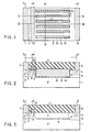
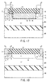
- FIGS. 1 to 4 show the main part of a lateral n-channel high breakdown voltage MOSFET according to a first embodiment of the present invention.
- FIG. 1 is a plan view thereof, and FIGS. 2 to 4 are cross-sectional views taken along lines II-II, III-III and IV-IV of FIG. 1, respectively. Please note that FIG. 1 does not show an insulation film 11 in order to present the layout of electrodes on an active layer.
- a p-type body region 2 is formed selectively on the surface of a high-resistance p - -type layer 1 made of monocrystalline silicon, and an n + -type source region 3 having a high impurity concentration is formed in the surface area of the body region 2.
- An n-type buffer region 4 is formed on the surface of the layer 1 at a given distance from the region 2, and an n + -type drain region 5 having a high impurity concentration is formed in the surface area of the buffer region 4.
- An n-type drift region 6 is formed between the p-type body region 2 and n-type buffer region 4 in order to obtain a high breakdown voltage.
- the dose of impurities of the n-type drift region 6 is 2 ⁇ 10 12 cm -2 to 2 ⁇ 10 13 cm -2 .
- the impurity concentration of the n-type buffer region 4 is higher than that of the n-type drift region 6, and the region 4 is provided for the purpose of relieving the concentration of electric fields and decreasing the resistance but not necessarily required.
- a source electrode 7 is formed on the p-type body region 2 so as to be connected with both the body region 2 and source region 3, and a drain electrode 8 is formed on the n + -type drain region 5.
- a gate electrode 10 is provided on the surface of the p-type body region 2 between the regions 3 and 6, with a gate oxide film 9 interposed therebetween. The surface of the resultant structure is protected by the insulation film 11 such as a silicon oxide film.
- a plurality of trenches 12 are formed in the drift region 6 between the regions 2 and 4.
- a silicon oxide film 13 having a thickness of 5 to 100 nm is formed on the sides and bottom of each of the trenches 12, and a semi-insulating polycrystalline silicon (SIPOS) film 14 having a high resistance is buried therein.
- the trenches 12 are formed by RIE (Reactive Ion Etching), the SIPOS film 14 is deposited by LPCVD, and an undesired portion is removed by dry etching such as RIE and CDE (Chemical Dry Etching).
- the trenches 12 each have a width w of 0.3 ⁇ m to 1 ⁇ m, and the distance d between adjacent trenches is 0.5 ⁇ m to 5 ⁇ m.
- the length L of each trench is equal to that of the drift region 6 and set in accordance with the breakdown voltage of the device. If the breakdown voltage is 500 V, the length L is about 50 ⁇ m.
- the depth of the trenches 12 is substantially equal to that of the drift region 6.
- the SIPOS film 14 is connected to the source electrode 7 at the source-side ends of the trenches 12 and it is connected to the drain electrode 8 at the drain-side ends thereof.
- the SIPOS film 14 can be connected to the gate electrode 10 at the source-ends.
- the resistance of the film 14 can be adjusted by the concentration of oxygen contained therein and the dimensions of the trenches 12.
- the most of the drift region 6 is divided into a plurality of long portions by the trenches 12. The section of FIG.
- the potentials corresponding to the voltage are distributed in the SIPOS film 14 in each of the trenches 12.
- a depletion layer expands not only from a pn junction between the part and the p - -type layer 1 or p-type body region 2, but also from an interface between the part and each of the trenches 12.
- the n-type drift region 12 is depleted more easily than in the structure with no trenches.
- the impurity concentration of the n-type drift region 6 is set higher than the optimum value in the device having no trenches, the drift region 6 will be depleted.
- the impurity concentration of the drift region 6 can be increased without lowering the breakdown voltage. Consequently, the resistance of the drift region can be decreased, as can be the on-resistance of the high breakdown voltage MOSFET. If the width w of each trench 12 is 1 ⁇ m, the distance d between adjacent trenches is 1 ⁇ m, and the depth thereof is about 4 ⁇ m, the impurity concentration of the n-type drift region 6 can be about four times as high as that in the device with no trenches, and the resistance of the drift region can be reduced to half.
- the resistance of the drift region can be reduced to half even if the width w and distance d are each 0.5 ⁇ m and the depth is about 1 ⁇ m.
- the trenches 12 having such dimensions can be formed by conventional lithography or RIE. If the width w and distance d are further decreased and the depth of the trenches are further increased, the dose of impurities of the n-type drift region 6 can be increased more than 2 ⁇ 10 13 cm -2 . It is advisable that the thickness of the silicon oxide film 13 be about one sixth of the distance d between the trenches 12.
- the SIPOS film 14 is buried into each of the trenches 12; however, it can be replaced with polysilicon whose impurity concentration is low.
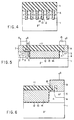
- FIG. 5 A high breakdown voltage MOSFET according to a second embodiment of the present invention is illustrated in FIG. 5 corresponding to FIG. 2 showing that of the first embodiment.
- a resistor 15 is inserted between the drain-side end of the SIPOS film 14 and the drain electrode 8.
- the values of the resistor 15 can be adjusted to control the distribution of potentials caused on the SIPOS film 14.
- a resistor can be inserted between the source-side end of the SIPOS film 14 and the source electrode 7 (or gate electrode 10), though not shown.
- FIG. 6 is a cross-sectional view of the structure of the periphery of the drain.
- the drain-side end of the SIPOS film 14 is extended and connected to the drain electrode 8 directly. That portion of the SIPOS film 14 which extends from the drain electrode 8 to the trenches 12 (i.e., the extended portion of the film 14) serves as the resistor 15.
- FIG. 7 is a plan view showing the major part of a high breakdown voltage MOSFET according to a third embodiment of the present invention.
- the sections taken along lines II-II, III-III, IV-IV in FIG. 7 correspond to those of FIGS. 2, 3 and 4, respectively.
- the trenches 12 are decreased in width on the drain side. If the n-type drift region 6 is thickened on the drain side, the breakdown voltage can be higher than that of the first embodiment. The same breakdown voltage increases the total amount of impurity of the n-type drift region 6 and lowers the on-resistance further.
- FIG. 8 is a plan view showing the major part of a high breakdown voltage MOSFET according to a fourth embodiment of the present invention.
- the sections taken along lines II-II, III-III, IV-IV in FIG. 8 correspond to those of FIGS. 2, 3 and 4, respectively.
- the trenches 12 are decreased in width gradually from the source toward the drain.
- the breakdown voltage can be higher than that of the first embodiment. The same breakdown voltage increases the total amount of impurity of the n-type drift region 6 and lowers the on-resistance further.
- FIGS. 9 to 13 illustrate the major part of a high breakdown voltage MOSFET according to a fifth embodiment of the present invention.
- FIG. 9 is a plan view thereof
- FIGS. 10 to 13 are cross-sectional views taken along lines X-X, XI-XI, XII-XII and XIII-XIII of FIG. 9, respectively.
- a second n-type drift region 16 is provided in the drift region 6 near the drain.
- the dose of the second drift region 16 is substantially the same as that of the drift region 6, and the depth thereof is equal to or greater than that of the drift region 6.
- the breakdown voltage can be made higher than that in the first embodiment by diffusing more impurities into the drain side of the n-type drift region than the source side thereof.
- the same breakdown voltage increases the total amount of impurity of the n-type drift region and lowers the on-resistance further.
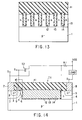
- FIGS. 14 and 15 are illustrations of a high breakdown voltage semiconductor device according to a sixth embodiment of the present invention.
- the device of the sixth embodiment includes the same high-breakdown voltage MOSFET T1 as that of the first embodiment, a second high-breakdown voltage MOSFET T2, and a resistor R1.
- the SIPOS film 14 and drain electrode 8 are not directly connected to each other.
- FIG. 14 shows that a load is connected to these constituting elements.
- the MOSFET T1 is illustrated by the sectional view corresponding to FIG. 2 of the first embodiment.
- FIG. 15 shows one example of the plane structure for accomplishing the structure shown in FIG. 14, and not any loads.
- a plurality of trenches 12 are formed in the drift region of the first high-breakdown voltage MOSFET T1 serving as the main element.
- the SIPOS film 14 is buried into each of the trenches 12, and one of the film 14 is connected to the gate electrode 10 of the MOSFET T1, while the other end thereof is connected to the drain electrode 17 of the second high-breakdown voltage MOSFET T2 and one end of the resistor R1.
- the sources of the first and second MOSFETs T1 and T2 are connected to each other, as are the gates thereof.
- the first and second MOSFETs T1 and T2 are designed so as to have substantially the same breakdown voltage. However, the second MOSFET T2 may have a high on-resistance.
- the other end of the resistor R1 is connected to a high-voltage DC power supply Vdd.
- a load is connected between the drain electrode 8 of the MOSFET T1 and the DC power supply Vdd.
- the first MOSFET T1 usually necessitates a breakdown voltage of about 400 V and the drift region requires a length of about 40 ⁇ m. If the resistance of the resistor R1 is r1, the resistance of parallel connection of all the SIPOS films 14 is r2, and the on-resistance of the second MOSFET T2 is r3, rl:r2:r3 is, for example, 39:3900:1. It is desirable that the absolute value of these resistances be larger.
- the ratio of r1 to r3 need not be 39:1 strictly and if it is not too small, the same advantage can be obtained.
- the drain voltage v has to be used within such a range that it exceeds a voltage of the trenches 12 or a voltage corresponding to the gate breakdown voltage.
- the gate When the gate is turned off, the same condition is obtained as in the second embodiment and the potentials are distributed on the SIPOS film in accordance with the ratio of r1 to r2.
- the potential at the drain-side end of the SIPOS film 14 is close to that of the drain, and the potential at the gate-side end thereof is equal to that of the gate.
- a potential gradient occurs on the entire SIPOS film 14 such that the potential increases gradually from the gate toward the drain.
- not only the breakdown voltage of the MOSFET T1 can be maintained, but also it can be increased further.
- a depletion layer expands from the interface between the n-type drift region 6, which is interposed between adjacent two trenches 12, and each side of the trench 12, so that the impurity concentration of the drift region 6 can be increased.
- the resistance of the drift region can be lowered by the two advantages: the impurity concentration of the drift region 6 can be set high, and electrons are induced on the sides of the trench 12 to cause a storage layer.
- the high breakdown voltage MOSFET of the third to fifth embodiments can be used for the MOSFET T1.
- FIGS. 16 to 18 show the major part of a high breakdown voltage MOSFET according to a seventh embodiment of the present invention.
- FIG. 16 is a plan view thereof
- FIGS. 17 and 18 are cross-sectional views taken along lines XVII-XVII and XVIII-XVIII of FIG. 16, respectively.
- the device of the first embodiment is modified and formed on an SOI substrate.
- a buried oxide film 19 is formed on a silicon substrate 18, and a high-resistance n - -type layer 20 is formed thereon.
- the same high breakdown voltage MOSFET as that of the first embodiment is formed on the SOI substrate.
- the impurity concentration of the n-type drift region 6 can be heightened without lowering the breakdown voltage; therefore, the drift region can be decreased in resistance.
- the n - -type layer 20 can be replaced with a high-resistance p-type layer.
- FIG. 19 is a cross-sectional view showing the major part of a vertical high-breakdown voltage MOSFET to which the present invention is applied as an eighth embodiment.
- An n-type drift layer 21 is formed in a monocrystalline silicon active layer, and a p-type body region 22 is formed selectively in the surface region of the drift layer 21.
- a high impurity concentration n + -type source region 23 is formed on the surface region of the region 22.
- a high impurity concentration n + -type drain region 24 is formed on the opposite surface of the drift layer 21.
- a source electrode 25 is formed on the p-type body region 22 so as to connect with both the regions 22 and 23, and a drain electrode 26 is formed in the n + -type drain region 24.
- a gate electrode 28 is provided on the surface of the p-type body region 22, which is interposed between the n + -type source region 23 and n-type drift layer 21, with a gate oxide film 27 therebetween.
- a plurality of trenches 29 are formed in the n-type drift layer 21 to such a depth as to reach the n + -type drain region 24.
- a silicon oxide film 30 having a thickness of about 5 nm to 100 nm is formed on the side wall of each of the trenches 29, and a high-resistance SIPOS film 31 is buried therein.
- the trenches 29 need not necessarily reach the n + -type drain region.
- the SIPOS film 31 is connected to the n + -type drain region 24 at the bottom and connected to the source electrode 25 on the top.
- a depletion layer expands from the interface between the n-type drift layer 21 and each of the trenches 29 in the drift layer 21 when a high voltage is applied, so that the impurity concentration of the drift layer 21 can be increased without lowering the breakdown voltage, thus decreasing the resistance of the drift layer.
- the present invention is applied to an n-channel high breakdown voltage MOSFET, has been described. It is needless to say that the present invention can be applied to a p-channel high breakdown voltage MOSFET. It can also be applied to another high breakdown voltage semiconductor device such as IGBT.
- the device can be constituted to have a trench gate like that shown in FIG. 20.
- a low impurity concentration polysilicon film can be used in place of the SIPOS film, as can be another high-resistance film.
- the impurity concentration of the drift region can be heightened and the on-resistance can be lowered by decreasing the drift resistance.
Abstract
Description
- The present invention relates to a high breakdown voltage semiconductor device and, more specifically, to a technique of reducing the resistance of a drift region of a high breakdown voltage MOSFET.
- A high breakdown voltage semiconductor device, such as a high breakdown voltage MOSFET and IGBT, has a drift region whose impurity concentration is relatively low in order to obtain a high breakdown voltage. If a high voltage is applied to the element in an off state, the drift region is depleted and the element withstands the high voltage. Since the drift region is low in impurity concentration, it increases in resistance and has a large share of on-resistance of the element. As the breakdown voltage heightens, the drift region increases in resistance; accordingly, the on-resistance of the element increases.
- A high breakdown voltage MOSFET, which has the structure as shown in FIG. 20 to decrease the resistance of a drift region, is proposed in T. Fujihira, "Theory of Semiconductor Superjunction Devices," Jpn. J. Appl. Phys., Vol. 36 (1997), pp 6254-6262. In this MOSFET, a
drift region 43 is formed between a p-type body region 41 and an n+-type drain region 42 in order to obtain a high breakdown voltage. Thedrift region 42 is constituted of p-type layers 44 and n-type layers 45 which are arranged alternately at small pitches in the channel width direction. If a high voltage is applied between the source and drain so as to make the drain positive, a depletion layer expands not only from both a pn junction between the p-type body region 41 and n-type layers 45 and a pn junction between a p-type layer 46 and the n-type layers 45, but also from a pn junction between the p-type layers 44 and n-type layers 45. For this reason, even though the impurity concentration of the n-type layers 45 is set higher than that of the drift region of a normal high breakdown voltage MOSFET, the n-type layers 45 can be depleted and the breakdown voltage can be maintained. With the structure of the MOSFET shown in FIG. 20, therefore, the resistance of the drift region can be lowered by increasing the impurity concentration of the n-type layers 45. - However, in order to achieve the above advantage, the impurity concentration of the n-
type layers 45 has to be at least two times as high as that of the normal high breakdown voltage MOSFET, provided that the P- and n-type layers layers - As described above, there is a problem in which the conventional superjunction elements are difficult to manufacture in actuality.
- The present invention has been developed in consideration of the above situation and its object is to provide a high breakdown voltage semiconductor device which is easy to manufacture and low in on-resistance.
- According to a first aspect of the present invention, there is provided a high breakdown voltage semiconductor device formed on a high resistance semiconductor layer, comprising a plurality of trenches formed like a stripe in a drift region in substantially parallel with a current flowing direction, an insulation film formed on a side and a bottom of each of the trenches, and a high resistance film buried into each of the trenches with the insulation film interposed therebetween, wherein the high resistance film is connected to one of source and gate electrodes directly or through a resistor near a source-end portion of each of the trenches, and the high resistance film is connected to a drain electrode directly or through a resistor near a drain-end portion of each of the trenches.
- In the high breakdown voltage semiconductor device according to the first aspect of the present invention, the high resistance film may be formed on one of a semi-insulating polycrystalline silicon and polysilicon.
- According to a second aspect of the present invention, there is provided a high breakdown voltage semiconductor device formed on a high resistance semiconductor layer of a first conductivity type, comprising a drift region of a second conductivity type selectively formed on a surface of the high resistance semiconductor layer, a plurality of trenches formed like a stripe in the drift region in substantially parallel with a current flowing direction, an insulation film formed on a side and a bottom of each of the trenches, and a high resistance film buried into each of the trenches with the insulation film interposed therebetween, wherein the high resistance film is connected to one of source and gate electrodes directly or through a resistor near a source-end portion of each of the trenches, and the high resistance film is connected to a drain electrode directly or through a resistor near a drain-end portion thereof.
- In the high breakdown voltage semiconductor device according to the second aspect of the present invention, the high resistance film may be formed on one of a semi-insulating polycrystalline silicon and polysilicon.
- According to a third aspect of the present invention, there is provided a high breakdown voltage semiconductor device including a first high breakdown voltage MOSFET, a second high breakdown voltage MOSFET, a resistor, comprising a plurality of trenches formed like a stripe in a drift region of the first high breakdown voltage MOSFET, in substantially parallel with a current flowing direction, an insulation film formed on a side and a bottom of each of the trenches, and a high resistance film buried into each of the trenches with the insulation film interposed therebetween, wherein the first high breakdown voltage MOSFET and the second high breakdown voltage MOSFET have a common source electrode and a common gate electrode, and one end of the high resistance film is connected to the common gate electrode, while another end thereof is connected to a drain electrode of the second high breakdown voltage MOSFET and one end of the resistor.
- In the high breakdown voltage semiconductor device according to the third aspect of the present invention, the high resistance film may be formed on one of a semi-insulating polycrystalline silicon and polysilicon.
- In the high breakdown voltage semiconductor device according to the third aspect of the present invention, the first high breakdown voltage MOSFET and the second high breakdown voltage MOSFET may be formed in a common semiconductor layer. The high resistance film may be formed on one of a semi-insulating polycrystalline silicon and polysilicon.
- According to a fourth aspect of the present invention, there is provided a high breakdown voltage semiconductor device formed on a high resistance semiconductor layer, comprising, a plurality of trenches formed like a stripe in a drift region in substantially parallel with a current flowing direction, an insulation film formed on a side of each of the trenches, and a high resistance film buried into each of the trenches, wherein the high resistance film is connected to one of source and gate electrodes directly or through a resistor near a source-end portion of each of the trenches, and the high resistance film is connected to a drain region near a drain-end portion of each of the trenches.
- In the high breakdown voltage semiconductor device according to the fourth aspect of the present invention, the high resistance film may be formed on one of a semi-insulating polycrystalline silicon and polysilicon.
- In the high breakdown voltage semiconductor device according to the present invention, a drift region is divided into a plurality of long regions each interposed between a plurality of trenches, and a depletion layer expands in a drift region from an interface between the drift region and each of the trenches when a reversed bias is applied. Thus, the impurity concentration of the drift region can be normally heightened to cause a high breakdown voltage. Consequently, the on-resistance can be lowered by increasing the impurity concentration of the drift region.
- This summary of the invention does not necessarily describe all necessary features so that the invention may also be a sub-combination of these described features.
- The invention can be more fully understood from the following detailed description when taken in conjunction with the accompanying drawings, in which:
- FIG. 1 is a plan view showing a high breakdown voltage MOSFET according to a first embodiment of the present invention;
- FIG. 2 is a cross-sectional view taken along line II-II of FIG. 1;
- FIG. 3 is a cross-sectional view taken along line III-III of FIG. 1;
- FIG. 4 is a cross-sectional view taken along line IV-IV of FIG. 1;
- FIG. 5 is a cross-sectional view showing a high breakdown voltage MOSFET according to a second embodiment of the present invention;
- FIG. 6 is a cross-sectional view partly showing a high breakdown voltage MOSFET according to the second embodiment of the present invention;
- FIG. 7 is a cross-sectional view showing a high breakdown voltage MOSFET according to a third embodiment of the present invention;
- FIG. 8 is a plan view showing a high breakdown voltage MOSFET according to a fourth embodiment of the present invention;
- FIG. 9 is a plan view showing a high breakdown voltage MOSFET according to a fifth embodiment of the present invention;
- FIG. 10 is a cross-sectional view taken along line X-X of FIG. 9;
- FIG. 11 is a cross-sectional view taken along line XI-XI of FIG. 9;
- FIG. 12 is a cross-sectional view taken along line XII-XII of FIG. 9;
- FIG. 13 is a cross-sectional view taken along line XIII-XIII of FIG. 9;
- FIG. 14 is an illustration of a high breakdown voltage semiconductor device according to a sixth embodiment of the present invention;
- FIG. 15 is a plan view of the high breakdown voltage semiconductor device according to the sixth embodiment of the present invention;
- FIG. 16 is a plan view showing a high breakdown voltage MOSFET according to a seventh embodiment of the present invention;
- FIG. 17 is a cross-sectional view taken along line XVII-XVII of FIG. 16;
- FIG. 18 is a cross-sectional view taken along line XVIII-XVIII of FIG. 16;
- FIG. 19 is a cross-sectional view showing a high breakdown voltage MOSFET according to an eighth embodiment of the present invention; and
- FIG. 20 is a cross-sectional view of a prior art superjunction high breakdown voltage MOSFET.
-
- Embodiments of the present invention will now be described with reference to the accompanying drawings.
- FIGS. 1 to 4 show the main part of a lateral n-channel high breakdown voltage MOSFET according to a first embodiment of the present invention. FIG. 1 is a plan view thereof, and FIGS. 2 to 4 are cross-sectional views taken along lines II-II, III-III and IV-IV of FIG. 1, respectively. Please note that FIG. 1 does not show an
insulation film 11 in order to present the layout of electrodes on an active layer. - A p-
type body region 2 is formed selectively on the surface of a high-resistance p--type layer 1 made of monocrystalline silicon, and an n+-type source region 3 having a high impurity concentration is formed in the surface area of thebody region 2. An n-type buffer region 4 is formed on the surface of thelayer 1 at a given distance from theregion 2, and an n+-type drain region 5 having a high impurity concentration is formed in the surface area of thebuffer region 4. An n-type drift region 6 is formed between the p-type body region 2 and n-type buffer region 4 in order to obtain a high breakdown voltage. The dose of impurities of the n-type drift region 6 is 2 × 1012 cm-2 to 2 × 1013 cm-2. The impurity concentration of the n-type buffer region 4 is higher than that of the n-type drift region 6, and theregion 4 is provided for the purpose of relieving the concentration of electric fields and decreasing the resistance but not necessarily required. Asource electrode 7 is formed on the p-type body region 2 so as to be connected with both thebody region 2 andsource region 3, and adrain electrode 8 is formed on the n+-type drain region 5. Agate electrode 10 is provided on the surface of the p-type body region 2 between theregions gate oxide film 9 interposed therebetween. The surface of the resultant structure is protected by theinsulation film 11 such as a silicon oxide film. - A plurality of
trenches 12 are formed in thedrift region 6 between theregions silicon oxide film 13 having a thickness of 5 to 100 nm is formed on the sides and bottom of each of thetrenches 12, and a semi-insulating polycrystalline silicon (SIPOS)film 14 having a high resistance is buried therein. Thetrenches 12 are formed by RIE (Reactive Ion Etching), theSIPOS film 14 is deposited by LPCVD, and an undesired portion is removed by dry etching such as RIE and CDE (Chemical Dry Etching). Thetrenches 12 each have a width w of 0.3 µm to 1 µm, and the distance d between adjacent trenches is 0.5 µm to 5 µm. The length L of each trench is equal to that of thedrift region 6 and set in accordance with the breakdown voltage of the device. If the breakdown voltage is 500 V, the length L is about 50 µm. The depth of thetrenches 12 is substantially equal to that of thedrift region 6. As diagrammatically shown in FIG. 2, theSIPOS film 14 is connected to thesource electrode 7 at the source-side ends of thetrenches 12 and it is connected to thedrain electrode 8 at the drain-side ends thereof. TheSIPOS film 14 can be connected to thegate electrode 10 at the source-ends. The resistance of thefilm 14 can be adjusted by the concentration of oxygen contained therein and the dimensions of thetrenches 12. The most of thedrift region 6 is divided into a plurality of long portions by thetrenches 12. The section of FIG. 3, which shows not thetrenches 12 but the portion obtained by dividing thedrift region 6, corresponds to that of a normal high-breakdown voltage MOSFET having no trenches. If, in the normal high-breakdown voltage MOSFET, a high voltage is applied in the OFF state, a depletion layer expands in an n-type drift region and a p--type layer to relieve the concentration of electric fields and thus to obtain a high breakdown voltage. - In the above high breakdown voltage MOSFET of the first embodiment, if a voltage is applied between the drain and source so as to set the drain at a high potential, the potentials corresponding to the voltage are distributed in the
SIPOS film 14 in each of thetrenches 12. In that part of the n-type drift region 6 which is interposed between twoadjacent trenches 12, a depletion layer expands not only from a pn junction between the part and the p--type layer 1 or p-type body region 2, but also from an interface between the part and each of thetrenches 12. The n-type drift region 12 is depleted more easily than in the structure with no trenches. Even though the impurity concentration of the n-type drift region 6 is set higher than the optimum value in the device having no trenches, thedrift region 6 will be depleted. Thus, the impurity concentration of thedrift region 6 can be increased without lowering the breakdown voltage. Consequently, the resistance of the drift region can be decreased, as can be the on-resistance of the high breakdown voltage MOSFET. If the width w of eachtrench 12 is 1 µm, the distance d between adjacent trenches is 1 µm, and the depth thereof is about 4 µm, the impurity concentration of the n-type drift region 6 can be about four times as high as that in the device with no trenches, and the resistance of the drift region can be reduced to half. Similarly, the resistance of the drift region can be reduced to half even if the width w and distance d are each 0.5 µm and the depth is about 1 µm. Thetrenches 12 having such dimensions can be formed by conventional lithography or RIE. If the width w and distance d are further decreased and the depth of the trenches are further increased, the dose of impurities of the n-type drift region 6 can be increased more than 2 × 1013 cm-2. It is advisable that the thickness of thesilicon oxide film 13 be about one sixth of the distance d between thetrenches 12. - In the first embodiment, the
SIPOS film 14 is buried into each of thetrenches 12; however, it can be replaced with polysilicon whose impurity concentration is low. - A high breakdown voltage MOSFET according to a second embodiment of the present invention is illustrated in FIG. 5 corresponding to FIG. 2 showing that of the first embodiment. In the second embodiment, a
resistor 15 is inserted between the drain-side end of theSIPOS film 14 and thedrain electrode 8. In order to make the impurity concentration of the n-type drift region 6 as high as possible, the values of theresistor 15 can be adjusted to control the distribution of potentials caused on theSIPOS film 14. Similarly, a resistor can be inserted between the source-side end of theSIPOS film 14 and the source electrode 7 (or gate electrode 10), though not shown. - The high breakdown voltage MOSFET of the second embodiment can actually be constituted as illustrated in FIG. 6. FIG. 6 is a cross-sectional view of the structure of the periphery of the drain. The drain-side end of the
SIPOS film 14 is extended and connected to thedrain electrode 8 directly. That portion of theSIPOS film 14 which extends from thedrain electrode 8 to the trenches 12 (i.e., the extended portion of the film 14) serves as theresistor 15. - FIG. 7 is a plan view showing the major part of a high breakdown voltage MOSFET according to a third embodiment of the present invention. The sections taken along lines II-II, III-III, IV-IV in FIG. 7 correspond to those of FIGS. 2, 3 and 4, respectively. In the third embodiment, the
trenches 12 are decreased in width on the drain side. If the n-type drift region 6 is thickened on the drain side, the breakdown voltage can be higher than that of the first embodiment. The same breakdown voltage increases the total amount of impurity of the n-type drift region 6 and lowers the on-resistance further. - FIG. 8 is a plan view showing the major part of a high breakdown voltage MOSFET according to a fourth embodiment of the present invention. The sections taken along lines II-II, III-III, IV-IV in FIG. 8 correspond to those of FIGS. 2, 3 and 4, respectively. In the fourth embodiment, the
trenches 12 are decreased in width gradually from the source toward the drain. As in the third embodiment, the breakdown voltage can be higher than that of the first embodiment. The same breakdown voltage increases the total amount of impurity of the n-type drift region 6 and lowers the on-resistance further. - FIGS. 9 to 13 illustrate the major part of a high breakdown voltage MOSFET according to a fifth embodiment of the present invention. FIG. 9 is a plan view thereof, and FIGS. 10 to 13 are cross-sectional views taken along lines X-X, XI-XI, XII-XII and XIII-XIII of FIG. 9, respectively. In the fifth embodiment, a second n-
type drift region 16 is provided in thedrift region 6 near the drain. The dose of thesecond drift region 16 is substantially the same as that of thedrift region 6, and the depth thereof is equal to or greater than that of thedrift region 6. As in the third and fourth embodiments, the breakdown voltage can be made higher than that in the first embodiment by diffusing more impurities into the drain side of the n-type drift region than the source side thereof. The same breakdown voltage increases the total amount of impurity of the n-type drift region and lowers the on-resistance further. - FIGS. 14 and 15 are illustrations of a high breakdown voltage semiconductor device according to a sixth embodiment of the present invention. The device of the sixth embodiment includes the same high-breakdown voltage MOSFET T1 as that of the first embodiment, a second high-breakdown voltage MOSFET T2, and a resistor R1. However, the
SIPOS film 14 anddrain electrode 8 are not directly connected to each other. FIG. 14 shows that a load is connected to these constituting elements. The MOSFET T1 is illustrated by the sectional view corresponding to FIG. 2 of the first embodiment. FIG. 15 shows one example of the plane structure for accomplishing the structure shown in FIG. 14, and not any loads. - As in the first embodiment, a plurality of
trenches 12 are formed in the drift region of the first high-breakdown voltage MOSFET T1 serving as the main element. TheSIPOS film 14 is buried into each of thetrenches 12, and one of thefilm 14 is connected to thegate electrode 10 of the MOSFET T1, while the other end thereof is connected to thedrain electrode 17 of the second high-breakdown voltage MOSFET T2 and one end of the resistor R1. The sources of the first and second MOSFETs T1 and T2 are connected to each other, as are the gates thereof. The first and second MOSFETs T1 and T2 are designed so as to have substantially the same breakdown voltage. However, the second MOSFET T2 may have a high on-resistance. The other end of the resistor R1 is connected to a high-voltage DC power supply Vdd. A load is connected between thedrain electrode 8 of the MOSFET T1 and the DC power supply Vdd. - Assuming that the operation voltage Vg of the gate is 5 V and the DC power supply voltage Vdd is 200 V, the first MOSFET T1 usually necessitates a breakdown voltage of about 400 V and the drift region requires a length of about 40 µm. If the resistance of the resistor R1 is r1, the resistance of parallel connection of all the
SIPOS films 14 is r2, and the on-resistance of the second MOSFET T2 is r3, rl:r2:r3 is, for example, 39:3900:1. It is desirable that the absolute value of these resistances be larger. - When the gate is turned on by applying a 5V-voltage thereto, the drain voltage v of the MOSFET T2 is set to 5V and so is the potential of all the
SIPOS films 14, since the ratio of r1 to r3 is 39:1 (=(Vdd-Vg):Vg). Thus, electrons are induced on the sides of thetrenches 12 to form a storage layer and decrease the drift resistance further, with the result that the on-resistance of the entire MOSFET T1 is lowered. The ratio of r1 to r3 need not be 39:1 strictly and if it is not too small, the same advantage can be obtained. If the ratio of r1 to r3 is set larger than that of (Vdd-Vg) to Vg, the advantage of causing the storage form to be formed becomes greater. However, the drain voltage v has to be used within such a range that it exceeds a voltage of thetrenches 12 or a voltage corresponding to the gate breakdown voltage. - When the gate is turned off, the same condition is obtained as in the second embodiment and the potentials are distributed on the SIPOS film in accordance with the ratio of r1 to r2. The potential at the drain-side end of the
SIPOS film 14 is close to that of the drain, and the potential at the gate-side end thereof is equal to that of the gate. A potential gradient occurs on theentire SIPOS film 14 such that the potential increases gradually from the gate toward the drain. As compared with a device having no trenches, not only the breakdown voltage of the MOSFET T1 can be maintained, but also it can be increased further. Like in the first embodiment, a depletion layer expands from the interface between the n-type drift region 6, which is interposed between adjacent twotrenches 12, and each side of thetrench 12, so that the impurity concentration of thedrift region 6 can be increased. - Consequently, according to the sixth embodiment, the resistance of the drift region can be lowered by the two advantages: the impurity concentration of the
drift region 6 can be set high, and electrons are induced on the sides of thetrench 12 to cause a storage layer. - In the sixth embodiment, the high breakdown voltage MOSFET of the third to fifth embodiments can be used for the MOSFET T1.
- FIGS. 16 to 18 show the major part of a high breakdown voltage MOSFET according to a seventh embodiment of the present invention. FIG. 16 is a plan view thereof, and FIGS. 17 and 18 are cross-sectional views taken along lines XVII-XVII and XVIII-XVIII of FIG. 16, respectively. In the seventh embodiment, the device of the first embodiment is modified and formed on an SOI substrate. A buried
oxide film 19 is formed on asilicon substrate 18, and a high-resistance n--type layer 20 is formed thereon. The same high breakdown voltage MOSFET as that of the first embodiment is formed on the SOI substrate. As in the first embodiment, the impurity concentration of the n-type drift region 6 can be heightened without lowering the breakdown voltage; therefore, the drift region can be decreased in resistance. The n--type layer 20 can be replaced with a high-resistance p-type layer. - FIG. 19 is a cross-sectional view showing the major part of a vertical high-breakdown voltage MOSFET to which the present invention is applied as an eighth embodiment. An n-
type drift layer 21 is formed in a monocrystalline silicon active layer, and a p-type body region 22 is formed selectively in the surface region of thedrift layer 21. A high impurity concentration n+-type source region 23 is formed on the surface region of theregion 22. A high impurity concentration n+-type drain region 24 is formed on the opposite surface of thedrift layer 21. Asource electrode 25 is formed on the p-type body region 22 so as to connect with both theregions drain electrode 26 is formed in the n+-type drain region 24. Agate electrode 28 is provided on the surface of the p-type body region 22, which is interposed between the n+-type source region 23 and n-type drift layer 21, with agate oxide film 27 therebetween. - A plurality of
trenches 29 are formed in the n-type drift layer 21 to such a depth as to reach the n+-type drain region 24. Asilicon oxide film 30 having a thickness of about 5 nm to 100 nm is formed on the side wall of each of thetrenches 29, and a high-resistance SIPOS film 31 is buried therein. Thetrenches 29 need not necessarily reach the n+-type drain region. The SIPOS film 31 is connected to the n+-type drain region 24 at the bottom and connected to thesource electrode 25 on the top. In the eighth embodiment, too, a depletion layer expands from the interface between the n-type drift layer 21 and each of thetrenches 29 in thedrift layer 21 when a high voltage is applied, so that the impurity concentration of thedrift layer 21 can be increased without lowering the breakdown voltage, thus decreasing the resistance of the drift layer. - An example where the present invention is applied to an n-channel high breakdown voltage MOSFET, has been described. It is needless to say that the present invention can be applied to a p-channel high breakdown voltage MOSFET. It can also be applied to another high breakdown voltage semiconductor device such as IGBT. The device can be constituted to have a trench gate like that shown in FIG. 20.
- As a film to be buried in the trenches, a low impurity concentration polysilicon film can be used in place of the SIPOS film, as can be another high-resistance film.
- According to the high breakdown voltage semiconductor device described above, the impurity concentration of the drift region can be heightened and the on-resistance can be lowered by decreasing the drift resistance.
Claims (10)
- A high breakdown voltage semiconductor device formed on a high resistance semiconductor layer, characterized by comprising:wherein the high resistance film (14) is connected to one of source and gate electrodes (7, 10) directly or through a resistor near a source-end portion of each of the trenches (12), and the high resistance film (14) is connected to a drain electrode (8) directly or through a resistor near a drain-end portion of each of the trenches (12).a plurality of trenches (12) formed like a stripe in a drift region (6) in substantially parallel with a current flowing direction;an insulation film (13) formed on a side and a bottom of each of the trenches; anda high resistance film (14) buried into each of the trenches with the insulation film interposed therebetween,
- A high breakdown voltage semiconductor device formed on a high resistance semiconductor layer of a first conductivity type, characterized by comprising:wherein the high resistance film (14) is connected to one of source and gate electrodes (7, 10) directly or through a resistor near a source-end portion of each of the trenches (12), and the high resistance film (14) is connected to a drain electrode (8) directly or through a resistor near a drain-end portion thereof.a drift region (6) of a second conductivity type selectively formed on a surface of the high resistance semiconductor layer;a plurality of trenches (12) formed like a stripe in the drift region in substantially parallel with a current flowing direction;an insulation film (13) formed on a side and a bottom of each of the trenches; anda high resistance film (14) buried into each of the trenches with the insulation film interposed therebetween,
- A high breakdown voltage semiconductor device including a first high breakdown voltage MOSFET (T1), a second high breakdown voltage MOSFET (T2), a resistor (R1), characterized by comprising:wherein the first high breakdown voltage MOSFET (T1) and the second high breakdown voltage MOSFET (T2) have a common source electrode (7) and a common gate electrode (10), and one end of the high resistance film (14) is connected to the common gate electrode (10), while another end thereof is connected to a drain electrode of the second high breakdown voltage MOSFET and one end of the resistor (R1).a plurality of trenches (12) formed like a stripe in a drift region (6) of the first high breakdown voltage MOSFET, in substantially parallel with a current flowing direction;an insulation film (13) formed on a side and a bottom of each of the trenches; anda high resistance film (14) buried into each of the trenches with the insulation film interposed therebetween,
- The high breakdown voltage semiconductor device according to claim 3, the first high breakdown voltage MOSFET (T1) and the second high breakdown voltage MOSFET (T2) are formed in a common semiconductor layer.
- A high breakdown voltage semiconductor device formed on a high resistance semiconductor layer, characterized by comprising:wherein the high resistance film (14) is connected to one of source and gate electrodes (7, 10) directly or through a resistor near a source-end portion of each of the trenches (12), and the high resistance film (14) is connected to a drain region (8) near a drain-end portion of each of the trenches (12).a plurality of trenches (12) formed like a stripe in a drift region (6) in substantially parallel with a current flowing direction;an insulation film (13) formed on a side of each of the trenches; anda high resistance film (14) buried into each of the trenches,
- The high breakdown voltage semiconductor device according to claim 1, characterized in that the high resistance film (14) is formed on one of a semi-insulating polycrystalline silicon and polysilicon.
- The high breakdown voltage semiconductor device according to claim 2, characterized in that the high resistance film (14) is formed on one of a semi-insulating polycrystalline silicon and polysilicon.
- The high breakdown voltage semiconductor device according to claim 3, characterized in that the high resistance film (14) is formed on one of a semi-insulating polycrystalline silicon and polysilicon.
- The high breakdown voltage semiconductor device according to claim 4, characterized in that the high resistance film (14) is formed on one of a semi-insulating polycrystalline silicon and polysilicon.
- The high breakdown voltage semiconductor device according to claim 5, characterized in that the high resistance film (14) is formed on one of a semi-insulating polycrystalline silicon and polysilicon.
Applications Claiming Priority (2)
| Application Number | Priority Date | Filing Date | Title |
|---|---|---|---|
| JP21531899A JP3971062B2 (en) | 1999-07-29 | 1999-07-29 | High voltage semiconductor device |
| JP21531899 | 1999-07-29 |
Publications (2)
| Publication Number | Publication Date |
|---|---|
| EP1073123A2 true EP1073123A2 (en) | 2001-01-31 |
| EP1073123A3 EP1073123A3 (en) | 2001-05-23 |
Family
ID=16670334
Family Applications (1)
| Application Number | Title | Priority Date | Filing Date |
|---|---|---|---|
| EP00306444A Withdrawn EP1073123A3 (en) | 1999-07-29 | 2000-07-28 | High withstand voltage semiconductor device |
Country Status (3)
| Country | Link |
|---|---|
| US (1) | US6353252B1 (en) |
| EP (1) | EP1073123A3 (en) |
| JP (1) | JP3971062B2 (en) |
Cited By (31)
| Publication number | Priority date | Publication date | Assignee | Title |
|---|---|---|---|---|
| WO2001059847A2 (en) | 2000-02-12 | 2001-08-16 | Koninklijke Philips Electronics N.V. | Insulated gate semiconductor device having field shaping regions |
| WO2001059846A1 (en) * | 2000-02-12 | 2001-08-16 | Koninklijke Philips Electronics N.V. | Semiconductor device with voltage divider for increased reverse blocking voltage |
| WO2003015178A1 (en) * | 2001-08-07 | 2003-02-20 | Koninklijke Philips Electronics N.V. | Trench bipolar transistor |
| EP1300886A2 (en) | 2001-09-07 | 2003-04-09 | Power Integrations, Inc. | High-voltage semiconductor devices |
| WO2003030262A2 (en) * | 2001-10-01 | 2003-04-10 | Koninklijke Philips Electronics N.V. | Silicon-on-insulator high voltage device structure |
| US6768171B2 (en) | 2000-11-27 | 2004-07-27 | Power Integrations, Inc. | High-voltage transistor with JFET conduction channels |
| US6787847B2 (en) | 2001-09-07 | 2004-09-07 | Power Integrations, Inc. | High-voltage vertical transistor with a multi-layered extended drain structure |
| US6838346B2 (en) | 2001-09-07 | 2005-01-04 | Power Integrations, Inc. | Method of fabricating a high-voltage transistor with a multi-layered extended drain structure |
| DE102004041198A1 (en) * | 2004-08-25 | 2006-03-02 | Infineon Technologies Austria Ag | Lateral semiconductor component to act as a field-effect transistor has a semiconductor body with first and second sides forming front and rear sides respectively |
| US7115958B2 (en) | 2001-10-29 | 2006-10-03 | Power Integrations, Inc. | Lateral power MOSFET for high switching speeds |
| DE102005035153A1 (en) * | 2005-07-27 | 2007-02-01 | Infineon Technologies Austria Ag | Semiconductor component e.g. power transistor, has drift zone, and drift control zone made of semiconductor material and arranged adjacent to drift zone in body, where accumulation dielectric is arranged between zones |
| DE102005046007A1 (en) * | 2005-09-26 | 2007-04-12 | Infineon Technologies Ag | Lateral compensation semiconductor component for use as high voltage transistor, has coupling layers for connection of compensation cells with each other, where layers are of p-type conduction and are in connection with source region |
| DE10240861B4 (en) * | 2002-09-04 | 2007-08-30 | Infineon Technologies Ag | By field effect controllable semiconductor device and method for its production |
| DE10313712B4 (en) * | 2003-03-27 | 2008-04-03 | Infineon Technologies Ag | Lateral field-controllable semiconductor device for RF applications |
| US7786533B2 (en) | 2001-09-07 | 2010-08-31 | Power Integrations, Inc. | High-voltage vertical transistor with edge termination structure |
| EP2261992A2 (en) | 2005-07-27 | 2010-12-15 | Infineon Technologies Austria AG | Semiconductor component with a drift region and with a drift control region |
| US7859037B2 (en) | 2007-02-16 | 2010-12-28 | Power Integrations, Inc. | Checkerboarded high-voltage vertical transistor layout |
| US8080848B2 (en) | 2006-05-11 | 2011-12-20 | Fairchild Semiconductor Corporation | High voltage semiconductor device with lateral series capacitive structure |
| US8110868B2 (en) | 2005-07-27 | 2012-02-07 | Infineon Technologies Austria Ag | Power semiconductor component with a low on-state resistance |
| DE102006009942B4 (en) * | 2006-03-03 | 2012-02-09 | Infineon Technologies Austria Ag | Lateral semiconductor device with low on-resistance |
| US8193565B2 (en) | 2008-04-18 | 2012-06-05 | Fairchild Semiconductor Corporation | Multi-level lateral floating coupled capacitor transistor structures |
| US8461648B2 (en) | 2005-07-27 | 2013-06-11 | Infineon Technologies Austria Ag | Semiconductor component with a drift region and a drift control region |
| US8653583B2 (en) | 2007-02-16 | 2014-02-18 | Power Integrations, Inc. | Sensing FET integrated with a high-voltage transistor |
| US8704296B2 (en) | 2012-02-29 | 2014-04-22 | Fairchild Semiconductor Corporation | Trench junction field-effect transistor |
| JP2014510399A (en) * | 2011-02-17 | 2014-04-24 | クゥアルコム・インコーポレイテッド | High-speed high-power semiconductor device |
| CN105990455A (en) * | 2015-03-16 | 2016-10-05 | 株式会社东芝 | Semiconductor device |
| US9601613B2 (en) | 2007-02-16 | 2017-03-21 | Power Integrations, Inc. | Gate pullback at ends of high-voltage vertical transistor structure |
| EP2056351B1 (en) * | 2007-10-31 | 2018-09-26 | Kabushiki Kaisha Toshiba | Semiconductor device |
| US10325988B2 (en) | 2013-12-13 | 2019-06-18 | Power Integrations, Inc. | Vertical transistor device structure with cylindrically-shaped field plates |
| CN112086517A (en) * | 2020-10-29 | 2020-12-15 | 珠海迈巨微电子有限责任公司 | Groove gate power semiconductor device and preparation method thereof |
| EP3520142B1 (en) * | 2016-09-28 | 2022-04-20 | Ecole Polytechnique Fédérale de Lausanne (EPFL) | Semiconductor device comprising a three-dimensional field plate |
Families Citing this family (81)
| Publication number | Priority date | Publication date | Assignee | Title |
|---|---|---|---|---|
| US6461918B1 (en) * | 1999-12-20 | 2002-10-08 | Fairchild Semiconductor Corporation | Power MOS device with improved gate charge performance |
| JP4528460B2 (en) * | 2000-06-30 | 2010-08-18 | 株式会社東芝 | Semiconductor element |
| US6696726B1 (en) * | 2000-08-16 | 2004-02-24 | Fairchild Semiconductor Corporation | Vertical MOSFET with ultra-low resistance and low gate charge |
| US7745289B2 (en) * | 2000-08-16 | 2010-06-29 | Fairchild Semiconductor Corporation | Method of forming a FET having ultra-low on-resistance and low gate charge |
| US6916745B2 (en) | 2003-05-20 | 2005-07-12 | Fairchild Semiconductor Corporation | Structure and method for forming a trench MOSFET having self-aligned features |
| US7345342B2 (en) * | 2001-01-30 | 2008-03-18 | Fairchild Semiconductor Corporation | Power semiconductor devices and methods of manufacture |
| US6710403B2 (en) * | 2002-07-30 | 2004-03-23 | Fairchild Semiconductor Corporation | Dual trench power MOSFET |
| US6803626B2 (en) | 2002-07-18 | 2004-10-12 | Fairchild Semiconductor Corporation | Vertical charge control semiconductor device |
| US7132712B2 (en) * | 2002-11-05 | 2006-11-07 | Fairchild Semiconductor Corporation | Trench structure having one or more diodes embedded therein adjacent a PN junction |
| US6713813B2 (en) | 2001-01-30 | 2004-03-30 | Fairchild Semiconductor Corporation | Field effect transistor having a lateral depletion structure |
| US6818513B2 (en) * | 2001-01-30 | 2004-11-16 | Fairchild Semiconductor Corporation | Method of forming a field effect transistor having a lateral depletion structure |
| FI120310B (en) * | 2001-02-13 | 2009-09-15 | Valtion Teknillinen | An improved method for producing secreted proteins in fungi |
| US6821824B2 (en) | 2001-02-21 | 2004-11-23 | Mitsubishi Denki Kabushiki Kaisha | Semiconductor device and method of manufacturing the same |
| US6853033B2 (en) * | 2001-06-05 | 2005-02-08 | National University Of Singapore | Power MOSFET having enhanced breakdown voltage |
| US6787872B2 (en) * | 2001-06-26 | 2004-09-07 | International Rectifier Corporation | Lateral conduction superjunction semiconductor device |
| US20030001216A1 (en) * | 2001-06-27 | 2003-01-02 | Motorola, Inc. | Semiconductor component and method of manufacturing |
| US7221011B2 (en) * | 2001-09-07 | 2007-05-22 | Power Integrations, Inc. | High-voltage vertical transistor with a multi-gradient drain doping profile |
| US7061066B2 (en) * | 2001-10-17 | 2006-06-13 | Fairchild Semiconductor Corporation | Schottky diode using charge balance structure |
| KR100859701B1 (en) * | 2002-02-23 | 2008-09-23 | 페어차일드코리아반도체 주식회사 | High voltage LDMOS transistor and method for fabricating the same |
| US7576388B1 (en) * | 2002-10-03 | 2009-08-18 | Fairchild Semiconductor Corporation | Trench-gate LDMOS structures |
| US6710418B1 (en) | 2002-10-11 | 2004-03-23 | Fairchild Semiconductor Corporation | Schottky rectifier with insulation-filled trenches and method of forming the same |
| DE10255359B4 (en) * | 2002-11-27 | 2008-09-04 | Infineon Technologies Ag | Transistor with filling areas in the source and / or drain region |
| US7652326B2 (en) * | 2003-05-20 | 2010-01-26 | Fairchild Semiconductor Corporation | Power semiconductor devices and methods of manufacture |
| US7005703B2 (en) * | 2003-10-17 | 2006-02-28 | Agere Systems Inc. | Metal-oxide-semiconductor device having improved performance and reliability |
| US7166890B2 (en) | 2003-10-21 | 2007-01-23 | Srikant Sridevan | Superjunction device with improved ruggedness |
| KR100994719B1 (en) * | 2003-11-28 | 2010-11-16 | 페어차일드코리아반도체 주식회사 | Superjunction semiconductor device |
| US7368777B2 (en) * | 2003-12-30 | 2008-05-06 | Fairchild Semiconductor Corporation | Accumulation device with charge balance structure and method of forming the same |
| US20050199918A1 (en) * | 2004-03-15 | 2005-09-15 | Daniel Calafut | Optimized trench power MOSFET with integrated schottky diode |
| US7352036B2 (en) * | 2004-08-03 | 2008-04-01 | Fairchild Semiconductor Corporation | Semiconductor power device having a top-side drain using a sinker trench |
| US7265415B2 (en) * | 2004-10-08 | 2007-09-04 | Fairchild Semiconductor Corporation | MOS-gated transistor with reduced miller capacitance |
| US7812441B2 (en) | 2004-10-21 | 2010-10-12 | Siliconix Technology C.V. | Schottky diode with improved surge capability |
| TWI278090B (en) * | 2004-10-21 | 2007-04-01 | Int Rectifier Corp | Solderable top metal for SiC device |
| US7834376B2 (en) | 2005-03-04 | 2010-11-16 | Siliconix Technology C. V. | Power semiconductor switch |
| US9419092B2 (en) * | 2005-03-04 | 2016-08-16 | Vishay-Siliconix | Termination for SiC trench devices |
| JP2008536316A (en) * | 2005-04-06 | 2008-09-04 | フェアチャイルド・セミコンダクター・コーポレーション | Trench gate field effect transistor and method of forming the same |
| GB0508407D0 (en) * | 2005-04-26 | 2005-06-01 | Ami Semiconductor Belgium Bvba | Alignment of trench for MOS |
| US7381603B2 (en) * | 2005-08-01 | 2008-06-03 | Semiconductor Components Industries, L.L.C. | Semiconductor structure with improved on resistance and breakdown voltage performance |
| US7276766B2 (en) * | 2005-08-01 | 2007-10-02 | Semiconductor Components Industries, L.L.C. | Semiconductor structure with improved on resistance and breakdown voltage performance |
| US7385248B2 (en) * | 2005-08-09 | 2008-06-10 | Fairchild Semiconductor Corporation | Shielded gate field effect transistor with improved inter-poly dielectric |
| US8368165B2 (en) | 2005-10-20 | 2013-02-05 | Siliconix Technology C. V. | Silicon carbide Schottky diode |
| US7659588B2 (en) * | 2006-01-26 | 2010-02-09 | Siliconix Technology C. V. | Termination for a superjunction device |
| US7446374B2 (en) | 2006-03-24 | 2008-11-04 | Fairchild Semiconductor Corporation | High density trench FET with integrated Schottky diode and method of manufacture |
| US7319256B1 (en) | 2006-06-19 | 2008-01-15 | Fairchild Semiconductor Corporation | Shielded gate trench FET with the shield and gate electrodes being connected together |
| WO2008016619A1 (en) * | 2006-07-31 | 2008-02-07 | Vishay-Siliconix | Molybdenum barrier metal for sic schottky diode and process of manufacture |
| US8564057B1 (en) * | 2007-01-09 | 2013-10-22 | Maxpower Semiconductor, Inc. | Power devices, structures, components, and methods using lateral drift, fixed net charge, and shield |
| CN101689562B (en) * | 2007-01-09 | 2013-05-15 | 威力半导体有限公司 | Semiconductor device |
| US7468536B2 (en) | 2007-02-16 | 2008-12-23 | Power Integrations, Inc. | Gate metal routing for transistor with checkerboarded layout |
| US7557406B2 (en) * | 2007-02-16 | 2009-07-07 | Power Integrations, Inc. | Segmented pillar layout for a high-voltage vertical transistor |
| US8587055B2 (en) * | 2007-02-23 | 2013-11-19 | Infineon Technologies Ag | Integrated circuit using a superjunction semiconductor device |
| JP5092174B2 (en) * | 2007-04-12 | 2012-12-05 | 三菱電機株式会社 | Semiconductor device |
| JP5138274B2 (en) * | 2007-05-25 | 2013-02-06 | 三菱電機株式会社 | Semiconductor device |
| EP2208229A4 (en) * | 2007-09-21 | 2011-03-16 | Fairchild Semiconductor | Superjunction structures for power devices and methods of manufacture |
| US7772668B2 (en) | 2007-12-26 | 2010-08-10 | Fairchild Semiconductor Corporation | Shielded gate trench FET with multiple channels |
| US20120273916A1 (en) | 2011-04-27 | 2012-11-01 | Yedinak Joseph A | Superjunction Structures for Power Devices and Methods of Manufacture |
| JP4602465B2 (en) * | 2008-12-04 | 2010-12-22 | 株式会社東芝 | Semiconductor device |
| JP2011114126A (en) * | 2009-11-26 | 2011-06-09 | Toshiba Corp | Semiconductor device and dc-dc converter |
| US8624302B2 (en) * | 2010-02-05 | 2014-01-07 | Fairchild Semiconductor Corporation | Structure and method for post oxidation silicon trench bottom shaping |
| US8319290B2 (en) | 2010-06-18 | 2012-11-27 | Fairchild Semiconductor Corporation | Trench MOS barrier schottky rectifier with a planar surface using CMP techniques |
| US8836028B2 (en) | 2011-04-27 | 2014-09-16 | Fairchild Semiconductor Corporation | Superjunction structures for power devices and methods of manufacture |
| US8772868B2 (en) | 2011-04-27 | 2014-07-08 | Fairchild Semiconductor Corporation | Superjunction structures for power devices and methods of manufacture |
| US8786010B2 (en) | 2011-04-27 | 2014-07-22 | Fairchild Semiconductor Corporation | Superjunction structures for power devices and methods of manufacture |
| US8673700B2 (en) * | 2011-04-27 | 2014-03-18 | Fairchild Semiconductor Corporation | Superjunction structures for power devices and methods of manufacture |
| US8963237B2 (en) * | 2011-09-17 | 2015-02-24 | Richtek Technology Corporation, R.O.C. | High voltage device and manufacturing method thereof |
| US9735243B2 (en) | 2013-11-18 | 2017-08-15 | Infineon Technologies Ag | Semiconductor device, integrated circuit and method of forming a semiconductor device |
| WO2014086479A1 (en) * | 2012-12-03 | 2014-06-12 | Infineon Technologies Ag | Semiconductor device, integrated circuit and method of forming a semiconductor device |
| US9799762B2 (en) | 2012-12-03 | 2017-10-24 | Infineon Technologies Ag | Semiconductor device and method of manufacturing a semiconductor device |
| JP2015008184A (en) * | 2013-06-25 | 2015-01-15 | 株式会社 日立パワーデバイス | Semiconductor device |
| US9123801B2 (en) * | 2013-09-16 | 2015-09-01 | Infineon Technologies Ag | Semiconductor device, integrated circuit and method of manufacturing a semiconductor device |
| US9461164B2 (en) | 2013-09-16 | 2016-10-04 | Infineon Technologies Ag | Semiconductor device and method of manufacturing the same |
| US9306058B2 (en) | 2013-10-02 | 2016-04-05 | Infineon Technologies Ag | Integrated circuit and method of manufacturing an integrated circuit |
| US9287404B2 (en) * | 2013-10-02 | 2016-03-15 | Infineon Technologies Austria Ag | Semiconductor device and method of manufacturing a semiconductor device with lateral FET cells and field plates |
| US9401399B2 (en) | 2013-10-15 | 2016-07-26 | Infineon Technologies Ag | Semiconductor device |
| US9543396B2 (en) | 2013-12-13 | 2017-01-10 | Power Integrations, Inc. | Vertical transistor device structure with cylindrically-shaped regions |
| US9520367B2 (en) * | 2014-08-20 | 2016-12-13 | Freescale Semiconductor, Inc. | Trenched Faraday shielding |
| JP6448258B2 (en) * | 2014-08-27 | 2019-01-09 | ルネサスエレクトロニクス株式会社 | Semiconductor device and manufacturing method thereof |
| CN106571388B (en) * | 2015-10-08 | 2018-10-12 | 无锡华润上华科技有限公司 | Transverse diffusion metal oxide semiconductor field effect pipe with RESURF structures |
| CN105529369B (en) * | 2016-03-08 | 2019-05-14 | 中国电子科技集团公司第二十四研究所 | A kind of semiconductor structure cell and power semiconductor |
| DE102016106578B4 (en) * | 2016-04-11 | 2021-11-04 | Infineon Technologies Austria Ag | Integrated transistor arrangement with a large number of lateral transistors |
| CN106024875B (en) * | 2016-07-19 | 2019-02-05 | 东南大学 | A kind of disconnected silicon-on-insulator landscape insulation bar double-pole-type transistor device of quick closing valve |
| DE102016113393A1 (en) * | 2016-07-20 | 2018-01-25 | Infineon Technologies Ag | A semiconductor device including a transistor array and a termination region, and methods of manufacturing such a semiconductor device |
| WO2023171454A1 (en) * | 2022-03-08 | 2023-09-14 | ローム株式会社 | Semiconductor device |
Citations (4)
| Publication number | Priority date | Publication date | Assignee | Title |
|---|---|---|---|---|
| GB2089118A (en) * | 1980-12-10 | 1982-06-16 | Philips Electronic Associated | Field-effect semiconductor device |
| US4796070A (en) * | 1987-01-15 | 1989-01-03 | General Electric Company | Lateral charge control semiconductor device and method of fabrication |
| US4947232A (en) * | 1980-03-22 | 1990-08-07 | Sharp Kabushiki Kaisha | High voltage MOS transistor |
| DE19848828A1 (en) * | 1998-10-22 | 2000-05-04 | Siemens Ag | Semiconductor device, especially a power MOSFET, Schottky diode or JFET, has a semi-insulating layer parallel to a drift region between two spaced electrodes |
Family Cites Families (5)
| Publication number | Priority date | Publication date | Assignee | Title |
|---|---|---|---|---|
| US5294824A (en) | 1992-07-31 | 1994-03-15 | Motorola, Inc. | High voltage transistor having reduced on-resistance |
| JP2561413B2 (en) * | 1993-02-23 | 1996-12-11 | 日産自動車株式会社 | Semiconductor device |
| DE4309764C2 (en) | 1993-03-25 | 1997-01-30 | Siemens Ag | Power MOSFET |
| BE1007283A3 (en) | 1993-07-12 | 1995-05-09 | Philips Electronics Nv | Semiconductor device with most with an extended drain area high voltage. |
| JPH09266311A (en) | 1996-01-22 | 1997-10-07 | Fuji Electric Co Ltd | Semiconductor device and its manufacture |
-
1999
- 1999-07-29 JP JP21531899A patent/JP3971062B2/en not_active Expired - Fee Related
-
2000
- 2000-07-28 US US09/628,715 patent/US6353252B1/en not_active Expired - Fee Related
- 2000-07-28 EP EP00306444A patent/EP1073123A3/en not_active Withdrawn
Patent Citations (4)
| Publication number | Priority date | Publication date | Assignee | Title |
|---|---|---|---|---|
| US4947232A (en) * | 1980-03-22 | 1990-08-07 | Sharp Kabushiki Kaisha | High voltage MOS transistor |
| GB2089118A (en) * | 1980-12-10 | 1982-06-16 | Philips Electronic Associated | Field-effect semiconductor device |
| US4796070A (en) * | 1987-01-15 | 1989-01-03 | General Electric Company | Lateral charge control semiconductor device and method of fabrication |
| DE19848828A1 (en) * | 1998-10-22 | 2000-05-04 | Siemens Ag | Semiconductor device, especially a power MOSFET, Schottky diode or JFET, has a semi-insulating layer parallel to a drift region between two spaced electrodes |
Non-Patent Citations (1)
| Title |
|---|
| FUJIHIRA T: "THEORY OF SEMICONDUCTOR SUPERJUNCTION DEVICES" JAPANESE JOURNAL OF APPLIED PHYSICS, PART 1, vol. 36, no. 10, October 1997 (1997-10), pages 6254-6262, XP000918328 TOKYO, JP ISSN: 0021-4922 * |
Cited By (53)
| Publication number | Priority date | Publication date | Assignee | Title |
|---|---|---|---|---|
| WO2001059846A1 (en) * | 2000-02-12 | 2001-08-16 | Koninklijke Philips Electronics N.V. | Semiconductor device with voltage divider for increased reverse blocking voltage |
| WO2001059847A3 (en) * | 2000-02-12 | 2002-03-28 | Koninkl Philips Electronics Nv | Insulated gate semiconductor device having field shaping regions |
| WO2001059847A2 (en) | 2000-02-12 | 2001-08-16 | Koninklijke Philips Electronics N.V. | Insulated gate semiconductor device having field shaping regions |
| US6768171B2 (en) | 2000-11-27 | 2004-07-27 | Power Integrations, Inc. | High-voltage transistor with JFET conduction channels |
| WO2003015178A1 (en) * | 2001-08-07 | 2003-02-20 | Koninklijke Philips Electronics N.V. | Trench bipolar transistor |
| US6777780B2 (en) | 2001-08-07 | 2004-08-17 | Koninklijke Philips Electronics N.V. | Trench bipolar transistor |
| US7786533B2 (en) | 2001-09-07 | 2010-08-31 | Power Integrations, Inc. | High-voltage vertical transistor with edge termination structure |
| US6882005B2 (en) | 2001-09-07 | 2005-04-19 | Power Integrations, Inc. | High-voltage vertical transistor with a multi-layered extended drain structure |
| US7745291B2 (en) | 2001-09-07 | 2010-06-29 | Power Integrations, Inc. | Method of fabricating a high-voltage transistor with an extended drain structure |
| EP1521307A3 (en) * | 2001-09-07 | 2008-08-06 | Power Integrations, Inc. | High-voltage semiconductor devices |
| US6787847B2 (en) | 2001-09-07 | 2004-09-07 | Power Integrations, Inc. | High-voltage vertical transistor with a multi-layered extended drain structure |
| US6798020B2 (en) | 2001-09-07 | 2004-09-28 | Power Integrations, Inc. | High-voltage lateral transistor with a multi-layered extended drain structure |
| US6815293B2 (en) | 2001-09-07 | 2004-11-09 | Power Intergrations, Inc. | High-voltage lateral transistor with a multi-layered extended drain structure |
| US6838346B2 (en) | 2001-09-07 | 2005-01-04 | Power Integrations, Inc. | Method of fabricating a high-voltage transistor with a multi-layered extended drain structure |
| EP1521307A2 (en) | 2001-09-07 | 2005-04-06 | Power Integrations, Inc. | High-voltage semiconductor devices |
| EP1300886A3 (en) * | 2001-09-07 | 2004-02-18 | Power Integrations, Inc. | High-voltage semiconductor devices |
| US6987299B2 (en) | 2001-09-07 | 2006-01-17 | Power Integrations, Inc. | High-voltage lateral transistor with a multi-layered extended drain structure |
| US7829944B2 (en) | 2001-09-07 | 2010-11-09 | Power Integrations, Inc. | High-voltage vertical transistor with a multi-layered extended drain structure |
| US8552496B2 (en) | 2001-09-07 | 2013-10-08 | Power Integrations, Inc. | High-voltage vertical transistor with edge termination structure |
| EP1300886A2 (en) | 2001-09-07 | 2003-04-09 | Power Integrations, Inc. | High-voltage semiconductor devices |
| KR100904785B1 (en) * | 2001-10-01 | 2009-06-25 | 엔엑스피 비 브이 | Silicon-on-insulator high voltage device structure |
| WO2003030262A2 (en) * | 2001-10-01 | 2003-04-10 | Koninklijke Philips Electronics N.V. | Silicon-on-insulator high voltage device structure |
| WO2003030262A3 (en) * | 2001-10-01 | 2003-06-05 | Koninkl Philips Electronics Nv | Silicon-on-insulator high voltage device structure |
| US7115958B2 (en) | 2001-10-29 | 2006-10-03 | Power Integrations, Inc. | Lateral power MOSFET for high switching speeds |
| DE10240861B4 (en) * | 2002-09-04 | 2007-08-30 | Infineon Technologies Ag | By field effect controllable semiconductor device and method for its production |
| DE10313712B4 (en) * | 2003-03-27 | 2008-04-03 | Infineon Technologies Ag | Lateral field-controllable semiconductor device for RF applications |
| US7423325B2 (en) | 2003-03-27 | 2008-09-09 | Infineon Technologies Ag | Lateral field-effect-controllable semiconductor component for RF applications |
| DE102004041198B4 (en) * | 2004-08-25 | 2016-06-09 | Infineon Technologies Austria Ag | Lateral semiconductor device with a field electrode and a discharge structure |
| DE102004041198A1 (en) * | 2004-08-25 | 2006-03-02 | Infineon Technologies Austria Ag | Lateral semiconductor component to act as a field-effect transistor has a semiconductor body with first and second sides forming front and rear sides respectively |
| EP2261992A2 (en) | 2005-07-27 | 2010-12-15 | Infineon Technologies Austria AG | Semiconductor component with a drift region and with a drift control region |
| US9190511B2 (en) | 2005-07-27 | 2015-11-17 | Infineon Technologies Austria Ag | Semiconductor component with a drift region and a drift control region |
| EP2267785A2 (en) | 2005-07-27 | 2010-12-29 | Infineon Technologies Austria AG | Semiconductor component with a drift region and with a drift control region |
| DE102005035153A1 (en) * | 2005-07-27 | 2007-02-01 | Infineon Technologies Austria Ag | Semiconductor component e.g. power transistor, has drift zone, and drift control zone made of semiconductor material and arranged adjacent to drift zone in body, where accumulation dielectric is arranged between zones |
| US8110868B2 (en) | 2005-07-27 | 2012-02-07 | Infineon Technologies Austria Ag | Power semiconductor component with a low on-state resistance |
| US8643086B2 (en) | 2005-07-27 | 2014-02-04 | Infineon Technologies Austria Ag | Semiconductor component with high breakthrough tension and low forward resistance |
| US8461648B2 (en) | 2005-07-27 | 2013-06-11 | Infineon Technologies Austria Ag | Semiconductor component with a drift region and a drift control region |
| DE102005046007A1 (en) * | 2005-09-26 | 2007-04-12 | Infineon Technologies Ag | Lateral compensation semiconductor component for use as high voltage transistor, has coupling layers for connection of compensation cells with each other, where layers are of p-type conduction and are in connection with source region |
| DE102005046007B4 (en) | 2005-09-26 | 2018-06-07 | Infineon Technologies Ag | Lateral compensating semiconductor device with coupled compensation cells |
| DE102006009942B4 (en) * | 2006-03-03 | 2012-02-09 | Infineon Technologies Austria Ag | Lateral semiconductor device with low on-resistance |
| US8080848B2 (en) | 2006-05-11 | 2011-12-20 | Fairchild Semiconductor Corporation | High voltage semiconductor device with lateral series capacitive structure |
| US8653583B2 (en) | 2007-02-16 | 2014-02-18 | Power Integrations, Inc. | Sensing FET integrated with a high-voltage transistor |
| US7859037B2 (en) | 2007-02-16 | 2010-12-28 | Power Integrations, Inc. | Checkerboarded high-voltage vertical transistor layout |
| US9601613B2 (en) | 2007-02-16 | 2017-03-21 | Power Integrations, Inc. | Gate pullback at ends of high-voltage vertical transistor structure |
| EP2056351B1 (en) * | 2007-10-31 | 2018-09-26 | Kabushiki Kaisha Toshiba | Semiconductor device |
| US8193565B2 (en) | 2008-04-18 | 2012-06-05 | Fairchild Semiconductor Corporation | Multi-level lateral floating coupled capacitor transistor structures |
| JP2014510399A (en) * | 2011-02-17 | 2014-04-24 | クゥアルコム・インコーポレイテッド | High-speed high-power semiconductor device |
| US8704296B2 (en) | 2012-02-29 | 2014-04-22 | Fairchild Semiconductor Corporation | Trench junction field-effect transistor |
| US10325988B2 (en) | 2013-12-13 | 2019-06-18 | Power Integrations, Inc. | Vertical transistor device structure with cylindrically-shaped field plates |
| US9508798B2 (en) | 2015-03-16 | 2016-11-29 | Kabushiki Kaisha Toshiba | Semiconductor device |
| CN105990455A (en) * | 2015-03-16 | 2016-10-05 | 株式会社东芝 | Semiconductor device |
| EP3520142B1 (en) * | 2016-09-28 | 2022-04-20 | Ecole Polytechnique Fédérale de Lausanne (EPFL) | Semiconductor device comprising a three-dimensional field plate |
| US11476357B2 (en) | 2016-09-28 | 2022-10-18 | Ecole Polytechnique Federale De Lausanne (Epfl) | Semiconductor device comprising a three-dimensional field plate |
| CN112086517A (en) * | 2020-10-29 | 2020-12-15 | 珠海迈巨微电子有限责任公司 | Groove gate power semiconductor device and preparation method thereof |
Also Published As
| Publication number | Publication date |
|---|---|
| EP1073123A3 (en) | 2001-05-23 |
| JP3971062B2 (en) | 2007-09-05 |
| US6353252B1 (en) | 2002-03-05 |
| JP2001044424A (en) | 2001-02-16 |
Similar Documents
| Publication | Publication Date | Title |
|---|---|---|
| US6353252B1 (en) | High breakdown voltage semiconductor device having trenched film connected to electrodes | |
| US7002211B2 (en) | Lateral super-junction semiconductor device | |
| JP2529717B2 (en) | High voltage MOS transistor | |
| US6512268B1 (en) | Super-junction semiconductor device | |
| JP4087248B2 (en) | Trench gate field effect transistor and method of manufacturing the same | |
| US5473180A (en) | Semiconductor device with an MOST provided with an extended drain region for high voltages | |
| US6700141B2 (en) | Semiconductor device | |
| US6444527B1 (en) | Method of operation of punch-through field effect transistor | |
| US5306656A (en) | Method for reducing on resistance and improving current characteristics of a MOSFET | |
| US5844275A (en) | High withstand-voltage lateral MOSFET with a trench and method of producing the same | |
| US6833585B2 (en) | High voltage lateral DMOS transistor having low on-resistance and high breakdown voltage | |
| US5885878A (en) | Lateral trench MISFET and method of manufacturing the same | |
| US5932897A (en) | High-breakdown-voltage semiconductor device | |
| US6849880B1 (en) | Power semiconductor device | |
| US7476932B2 (en) | U-shape metal-oxide-semiconductor (UMOS) gate structure for high power MOS-based semiconductor devices | |
| US9373714B2 (en) | Extended-drain MOS transistor in a thin film on insulator | |
| US7898024B2 (en) | Semiconductor device and method for manufacturing the same | |
| KR100381845B1 (en) | Long channel trench-gated power mosfet having fully depleted body region | |
| US7696599B2 (en) | Trench MOSFET | |
| US20080087949A1 (en) | Semiconductor device and method of manufacturing the same | |
| US6339243B1 (en) | High voltage device and method for fabricating the same | |
| JP2007520873A (en) | Trench MOS structure | |
| JP4023062B2 (en) | Semiconductor device | |
| US10043899B1 (en) | Laterally diffused MOSFET for embedded memory applications | |
| JP2003008029A (en) | Lateral semiconductor device |
Legal Events
| Date | Code | Title | Description |
|---|---|---|---|
| PUAI | Public reference made under article 153(3) epc to a published international application that has entered the european phase |
Free format text: ORIGINAL CODE: 0009012 |
|
| 17P | Request for examination filed |
Effective date: 20000825 |
|
| AK | Designated contracting states |
Kind code of ref document: A2 Designated state(s): DE FR GB |
|
| AX | Request for extension of the european patent |
Free format text: AL;LT;LV;MK;RO;SI |
|
| PUAL | Search report despatched |
Free format text: ORIGINAL CODE: 0009013 |
|
| AK | Designated contracting states |
Kind code of ref document: A3 Designated state(s): AT BE CH CY DE DK ES FI FR GB GR IE IT LI LU MC NL PT SE |
|
| AX | Request for extension of the european patent |
Free format text: AL;LT;LV;MK;RO;SI |
|
| RIC1 | Information provided on ipc code assigned before grant |
Free format text: 7H 01L 29/78 A, 7H 01L 29/41 B, 7H 01L 29/49 B, 7H 01L 27/06 B |
|
| AKX | Designation fees paid |
Free format text: DE FR GB |
|
| 17Q | First examination report despatched |
Effective date: 20040702 |
|
| RIC1 | Information provided on ipc code assigned before grant |
Ipc: H01L 29/78 20060101AFI20101110BHEP Ipc: H01L 29/36 20060101ALN20101110BHEP Ipc: H01L 27/06 20060101ALI20101110BHEP Ipc: H01L 29/08 20060101ALN20101110BHEP Ipc: H01L 29/49 20060101ALI20101110BHEP Ipc: H01L 29/41 20060101ALI20101110BHEP Ipc: H01L 29/739 20060101ALI20101110BHEP |
|
| RTI1 | Title (correction) |
Free format text: HIGH WITHSTAND VOLTAGE SEMICONDUCTOR DEVICES |
|
| GRAP | Despatch of communication of intention to grant a patent |
Free format text: ORIGINAL CODE: EPIDOSNIGR1 |
|
| STAA | Information on the status of an ep patent application or granted ep patent |
Free format text: STATUS: THE APPLICATION IS DEEMED TO BE WITHDRAWN |
|
| 18D | Application deemed to be withdrawn |
Effective date: 20110514 |