EP1091386A2 - Illumination system for electron beam lithography tool - Google Patents
Illumination system for electron beam lithography tool Download PDFInfo
- Publication number
- EP1091386A2 EP1091386A2 EP00308685A EP00308685A EP1091386A2 EP 1091386 A2 EP1091386 A2 EP 1091386A2 EP 00308685 A EP00308685 A EP 00308685A EP 00308685 A EP00308685 A EP 00308685A EP 1091386 A2 EP1091386 A2 EP 1091386A2
- Authority
- EP
- European Patent Office
- Prior art keywords
- illumination system
- system component
- lens array
- electron
- electron gun
- Prior art date
- Legal status (The legal status is an assumption and is not a legal conclusion. Google has not performed a legal analysis and makes no representation as to the accuracy of the status listed.)
- Granted
Links
Images


Classifications
-
- H—ELECTRICITY
- H01—ELECTRIC ELEMENTS
- H01J—ELECTRIC DISCHARGE TUBES OR DISCHARGE LAMPS
- H01J37/00—Discharge tubes with provision for introducing objects or material to be exposed to the discharge, e.g. for the purpose of examination or processing thereof
- H01J37/02—Details
- H01J37/04—Arrangements of electrodes and associated parts for generating or controlling the discharge, e.g. electron-optical arrangement, ion-optical arrangement
- H01J37/06—Electron sources; Electron guns
- H01J37/065—Construction of guns or parts thereof
-
- H—ELECTRICITY
- H01—ELECTRIC ELEMENTS
- H01L—SEMICONDUCTOR DEVICES NOT COVERED BY CLASS H10
- H01L21/00—Processes or apparatus adapted for the manufacture or treatment of semiconductor or solid state devices or of parts thereof
- H01L21/02—Manufacture or treatment of semiconductor devices or of parts thereof
- H01L21/027—Making masks on semiconductor bodies for further photolithographic processing not provided for in group H01L21/18 or H01L21/34
-
- H—ELECTRICITY
- H01—ELECTRIC ELEMENTS
- H01J—ELECTRIC DISCHARGE TUBES OR DISCHARGE LAMPS
- H01J37/00—Discharge tubes with provision for introducing objects or material to be exposed to the discharge, e.g. for the purpose of examination or processing thereof
- H01J37/02—Details
- H01J37/04—Arrangements of electrodes and associated parts for generating or controlling the discharge, e.g. electron-optical arrangement, ion-optical arrangement
- H01J37/10—Lenses
- H01J37/12—Lenses electrostatic
-
- H—ELECTRICITY
- H01—ELECTRIC ELEMENTS
- H01J—ELECTRIC DISCHARGE TUBES OR DISCHARGE LAMPS
- H01J2237/00—Discharge tubes exposing object to beam, e.g. for analysis treatment, etching, imaging
- H01J2237/10—Lenses
- H01J2237/12—Lenses electrostatic
- H01J2237/1205—Microlenses
-
- H—ELECTRICITY
- H01—ELECTRIC ELEMENTS
- H01J—ELECTRIC DISCHARGE TUBES OR DISCHARGE LAMPS
- H01J2237/00—Discharge tubes exposing object to beam, e.g. for analysis treatment, etching, imaging
- H01J2237/30—Electron or ion beam tubes for processing objects
- H01J2237/317—Processing objects on a microscale
- H01J2237/3175—Lithography
- H01J2237/31774—Multi-beam
Definitions
- This invention relates to an illumination system for an electron beam lithography apparatus used for the manufacture of semiconductor integrated circuits.
- Electron beam exposure tools have been used for lithography in semiconductor processing for more than two decades.
- the first e-beam exposure tools were based on the flying spot concept of a highly focused beam, raster scanned over the object plane.
- the electron beam is modulated as it scans so that the beam itself generates the lithographic pattern.
- These tools have been widely used for high precision tasks, such as lithographic mask making, but the raster scan mode is found to be too slow to enable the high throughput required in semiconductor wafer processing.
- the electron source in this equipment is similar to that used in electron microscopes, i.e., a high brightness source focused to a small spot beam.
- the requirements for the electron beam source in SCALPEL exposure tools differ significantly from those of a conventional focused beam exposure tool, or a conventional TEM or SEM. While high resolution imaging is still a primary goal, this must be achieved at relatively high (10-100 ⁇ A) gun currents in order to realize economic wafer throughput.
- the axial brightness required is relatively low, e.g., 10 2 to 10 4 Acm -2 sr -1 , as compared with a value of 10 6 to 10 9 Acm -2 sr -1 for a typical focused beam source.
- the beam flux over the larger area must be highly uniform to obtain the required lithographic dose latitude and CD control.
- the present invention is directed to a charged particle illumination system component for an electron beam exposure tool and an electron beam exposure tool that provides independent emittance control by placing a lens array, which acts as an "emittance controller", in the illumination system component.
- a conductive mesh grid under negative bias is placed in the SCALPEL lithography tool kept at ground potential, forming a multitude of microlenses resembling an optical "fly's eye” lens.
- the mesh grid splits an incoming solid electron beam into a multitude of subbeams, such that the outgoing beam emittance is different from the incoming beam emittance, while beam total current remains unchanged.
- the mesh grid enables beam emittance control without affecting beam current.
- the illumination system component is an electron gun.
- the illumination system component is a liner tube, connectable to a conventional electron gun.
- each opening in the mesh acts as a microlens, or lenslet, creating its own virtual source, or cross-over, having diameter d, on one side of the mesh grid.
- Each individual subbeam takes up geometrical space close to L, where L equals the mesh pitch.
- the mesh grid includes multiple (for example, two, three, or more) meshes.
- the outward two meshes may have a curved shape; such a lens would enable beam emittance control and also reduce spherical aberration.
- the lens array is a continuous lens made of foil.
- a conventional Wehnelt electron gun assembly is shown with base 11, cathode support arms 12, cathode filament 13, a Wehnelt electrode including Wehnelt horizontal support arms 15 and conventional Wehnelt aperture 16.
- the base 11 may be ceramic
- the support members 12 may be tantalum, steel, or molybdenum.
- the filament 13 may be tungsten wire
- the material forming the Wehnelt aperture 16 may be steel or tantalum
- the electron emitter 14 is, e.g., a tantalum disk.
- the effective area of the electron emitter is typically in the range of 0.1-5.0 mm 2 .
- the electron emitter 14 is preferably a disk with a diameter in the range of 0.05-3.0 mm.
- the anode is shown schematically at 17, including anode aperture 17a, the electron beam at 18, and a drift space at 19.
- the beam control apparatus which is conventional and well known in the art, is not shown. It will be appreciated by those skilled in the art that the dimensions in the figures are not necessarily to scale.
- An important feature of the electron source of SCALPEL exposure tools is relatively low electron beam brightness, as mentioned earlier. For most effective exposures, it is preferred that beam brightness be limited to a value less than 10 5 Acm -2 sr -1 . This is in contrast with conventional scanning electron beam exposure tools which are typically optimized for maximum brightness. See e.g., U.S. Patent No. 4,588,928 issued May 13, 1986 to Liu et al.
- a mesh grid 23 is disposed in the path of the electron emission 25 in the drift space 19.
- the mesh grid 23 is placed in the electrostatic field-free drift space 19, insulated from the drift tube, or liner 20, and it is biased to a specified potential Um.
- the potential difference between the mesh grid 23 and the liner 20 creates microlenses out of each opening in the mesh grid 23.
- the electron beam 18 is split into individual subbeams (beamlets), and each beamlet is focused moving through its respective mesh cell, or microlens.
- the mesh grid 23 is separated from the liner 20 by an insulator 24.
- the mesh grid 23 and the insulator 24 may both be part of a mesh holder.
- drift space 19 there is substantially no or no electric field present.
- the substantial absence of the electric field results in no acceleration or deceleration of electrons, hence the electrons are permitted to "drift", possibly in the presence of a magnetic field.
- Figures 2(a) and 2(b) illustrate variations on Figure 2.
- Figures 2(a) and 2(b) both show the mesh grid 23 within a liner 20 attached to an electron gun assembly 1.
- the liner 20 is attached to the electron gun assembly 1 via a liner flange 21 and an electron gun flange 16.
- the liner 20 is attached to the electron gun assembly 1 at weld 22.
- the liner 20 and electron gun assembly 1 could be attached by other techniques known to one of ordinary skill in the art, as long as the attachment is vacuum tight.
- the mesh grid 23 could be placed below the boundary between the liner flange 21 and the electron gun flange 16 or below the weld 22, within the electron gun assembly 1, as long as the mesh grid 23 remains within the drift space 19.
- FIGs 2(a) and 2(b) One advantage of the embodiments illustrates in Figures 2(a) and 2(b) is that they permit the use of conventional non-optimal electron guns.
- a conventional electron gun produces a beam which is too narrow and too non-uniform.
- the arrangements in Figures 2(a) and 2(b) permit increased performance utilizing a conventional electron gun, since the mesh grid 23 contained within the liner 20 improves the beam emittance by making it wider and more uniform, which is more suitable for SCALPEL applications.
- the effect of the mesh grid 23 is more clearly illustrated in Figure 2(c).
- FIG 3 The electron emission pattern from the Wehnelt gun of Figure 1, is shown in Figure 3. The relatively non-uniform, bell curve shaped output from the Wehnelt is evident.
- Figure 4 illustrates the electron beam emittance through the mesh grid 23. The emittance on the left side of the mesh grid 23 is low, whereas after passing through the mesh grid 23, the emittance of the electron beam is much higher.
- the screen element that forms the mesh grid 23 can have a variety of configurations. The simplest is a conventional woven screen with square apertures. However, the screen may have triangular shaped apertures, hexagonal close packed apertures, or even circular apertures. It can be woven or non-woven. Techniques for forming suitable screens from a continuous layer may occur to those skilled in the art. For example, multiple openings in a continuous metal sheet or foil can be produced by technique such as laser drilling. Fine meshes can also be formed by electroforming techniques.
- the mesh grid 23 should be electrically conducting but the material of the mesh is otherwise relatively inconsequential. Tantalum, tungsten, molybdenum, titanium, or even steel are suitable materials, as are some alloys as would be known to one skilled in the art.
- the mesh grid 23 preferably has a transparency in the range of 40-90%, with transparency defined as the two dimensional void space divided by the overall mesh grid area.
- the mesh grid has bars “b” of approximately 50 ⁇ m, and square cells with “C” approximately 200 ⁇ m.
- This mesh grid has a transparency of approximately 65%. Examples of mesh grid structures that were found suitable are represented by the examples in the following table. Cell dimension "C”, ⁇ m Bar width "b”, ⁇ m Grid #1 200 50 Grid #2 88 37 Grid #3 54 31
- the cell dimension "C” is the width of the opening in a mesh with a square opening.
- the dimension "C” is approximately the square root of the area of the opening. It is preferred that the openings be approximately symmetrical, i.e., square or round.
- the thickness t of the mesh grid is relatively immaterial except that the aspect ratio of the openings, C/t, is preferably greater than 1.
- a desirable relationship between the mesh grid parameters is given by: C:t>- 1.5
- the lens array may include more than one mesh.
- the lens array includes three meshes. The outer two meshes may be prepared having curved shape; such a lens would provide beam emittance control and decrease spherical aberration.
- outer two meshes may also be replaced with foils, such as an SiN foil, with a thickness of approximately 0.1 ⁇ m.
- foils such as an SiN foil
- Such a film would permit substantially no physical interaction (inelastic collisions), and therefore a transparency approaching 100%. Due to the large current being passed through the lens array (either mesh or continuous), the transparency is important. If a high percentage of the beam impacts the structure of the mesh or continuous film, the high current is likely to melt the mesh or continuous film.
- FIG. 5 is a more general representation of the optics of the present invention.
- 81 is the cathode of a standard high brightness electron gun, either a W hairpin, or a LaB 6 crystal or a BaO gun as used in for example a CRT.
- 82 is the gun lens formed by the Wehnelt electrode and the extraction field.
- 83 is the gun cross-over with diameter dg.
- 84 is the electron beam emerging from the gun, with half aperture angle ⁇ g as they appear looking back from where the beam has been accelerated to 100 kV.
- the lens array 80 is positioned.
- Each lenslet 85 creates an image 86 of the gun cross-over with size d i .
- Each subbeam 87 now has a half opening angle ⁇ .
- the emittance of the beam appears to be N ⁇ ⁇ 2 4 L 2 ⁇ 2 R where L is the pitch of the lenslets 85 and thus is the total area of the lens array 80.
- the new emittance of the beam is termed the effective emittance.
- the newly formed beam should include a reasonably large number of subbeams so that the subbeams will overlap at essential positions in the system such as the mask.
- Example 1 illustrates typical values.
- a LaB 6 gun of 0.2 mm diameter is used.
- the cross-over after the gun lens could be 60 ⁇ m, thus the emittance increase is a factor of eight using Grid #1 in Table 1.
- the lens array 80 may be the mesh grid 23 at potential V 1 , between liner 20 at potential V 0 as shown in Figure 6, or include two grids 23 and 23' at the potentials illustrated in Figure 6(a) or three grids 23, 23', 23'' at the potentials illustrated in Figure 6(b), or any other configuration which contains a grid mesh with an electrostatic field perpendicular to the gridplane.
- the focal distance of the lenslets 85 in Figure 5 is typically in the order of 4x Vacc/Efield, where Vacc is the acceleration potential of the electron beam and Efield the strength of the electrostatic field.
- Vacc is the acceleration potential of the electron beam
- Efield the strength of the electrostatic field.
- the distance between the gun cross-over and the lens array could be typically 100 mm, calling for a focal length of about 50 mm to create demagnified images.
- the field should be 10 kV/mm.
- the mesh grid 23 could be incorporated in the acceleration unit of the gun, between the cathode and the anode. This would have the additional advantage that the beam has not yet been accelerated to the full 100 kV at that point.
- the mesh grid 23 could also be incorporated in the electron gun in the Wehnelt-aperture 16 of Figure 2.
- the mesh pitch must again be much smaller than the cathode diameter. This would lead to lenslet sizes in the order of ⁇ m's.
- the present invention has been confirmed by computer simulation with both Charged Particle Optics (CPO, Bowring Consultant, Ltd., and Manchester University) and SOURCE (by MEBS, Ltd.) models.
- CPO Charged Particle Optics
- SOURCE by MEBS, Ltd.
- the mesh grid 23 is approximated by a series of circular slits.
- a lens including two grounded cylinders with a biased mesh in the gap between those cylinders is simulated.
- Figure 7 shows a detail of the SOURCE model, with fields. The lensfields are clearly visible in the openings in the mesh.
- Figure 8 illustrates the potential distribution in the plane of the mesh. Again, the multi-lens effect in the mesh grid can be clearly seen.
- the electron gun of the invention is most advantageously utilized as the electron source in a SCALPEL electron beam lithography machine.
- Fabrication of semiconductor devices on semiconductor wafers in current industry practice contemplates the exposure of polymer resist materials with fine line patterns of actinic radiation, in this case, electron beam radiation. This is achieved in conventional practice by directing the actinic radiation through a lithographic mask and onto a resist coated substrate.
- the mask may be positioned close to the substrate and the image of the mask projected onto the substrate for projection printing.
- SCALPEL lithography tools are characterized by high contrast patterns at very small linewidths, i.e., 0.1 ⁇ m or less. They produce high resolution images with wide process latitude, coupled with the high throughput of optical projection systems.
- the high throughput is made possible by using a flood beam of electrons to expose a relatively large area of the wafer. Electron beam optics, comprising standard magnetic field beam steering and focusing, are used to image the flood beam onto the lithographic mask, and thereafter, onto the substrate, i.e., the resist coated wafer.
- the lithographic mask is composed of regions of high electron scattering and regions of low electron scattering, which regions define the features desired in the mask pattern. Details of suitable mask structures can be found in U.S. Patents Nos. 5,079,112 issued Jan. 7, 1992, and 5,258,246 issued Nov. 2, 1993, both to Berger et al.
- the back focal plane filter functions by blocking the highly scattered electrons while passing the weakly scattered electrons, thus forming the image pattern on the substrate.
- the blocking filter thus absorbs the unwanted radiation in the image. This is in contrast to conventional lithography tools in which the unwanted radiation in the image is absorbed by the mask itself, contributing to heating and distortion of the mask, and to reduced mask lifetime.
- Lithographic mask 52 is illuminated with a uniform flood beam 51 of 100 keV electrons produced by the electron gun of Figure 2.
- the membrane mask 52 comprises regions 53 of high scattering material and regions 54 of low scattering material.
- the weakly scattered portions of the beam, i.e., rays 51a are focused by magnetic lens 55 through the aperture 57 of the back focal plane blocking filter 56.
- the back focal plane filter 56 may be a silicon wafer or other material suitable for blocking electrons.
- the highly scattered portions of the electron beam, represented here by rays 51b and 51c, are blocked by the back focal plane filter 56.
- Regions 60 replicate the features 54 of the lithographic mask 52, i.e., the regions to be exposed, and regions 61 replicate the features 53 of the lithographic mask, i.e., the regions that are not to be exposed. These regions are interchangeable, as is well known in the art, to produce either negative or positive resist patterns.
- a vital feature of the SCALPEL tool is the positioning of a blocking filter at or near the back focal plane of the electron beam image. Further details of SCALPEL systems can be found in U.S. Patents Nos. 5,079,112 issued Jan. 7, 1992, and 5,258,246 issued Nov. 2, 1993, both to Berger et al. These patents are incorporated herein by reference for such details that may be found useful for the practice of the invention.
- wehnelt emitter is intended to define a solid metal body with an approximately flat emitting surface, said flat emitting surface being symmetrical, i.e., having the shape of a circle or regular polygon.
- substrate is used herein to define the object plane of the electron beam exposure system whether or not there is a semiconductor workpiece present on the substrate.
- electron optics plane may be used to describe an x-y plane in space in the electron gun and the surface onto which the electron beam image is focused, i.e., the object plane where the semiconductor wafer is situated.
- an electron optical lens array is inserted into the illumination optics of the SCALPEL tool.
- the position of this lens array, or fly's eye lens, is such that each lenslet creates a beam cross-over with a smaller diameter d than the distance between the lenslets L, which increases the effective emittance of the beam by a factor (L/d) 2 .
- the electron optical lens array is a mesh grid with an electrostatic field perpendicular to the grid.
Abstract
Description
- This invention relates to an illumination system for an electron beam lithography apparatus used for the manufacture of semiconductor integrated circuits.
- Electron beam exposure tools have been used for lithography in semiconductor processing for more than two decades. The first e-beam exposure tools were based on the flying spot concept of a highly focused beam, raster scanned over the object plane. The electron beam is modulated as it scans so that the beam itself generates the lithographic pattern. These tools have been widely used for high precision tasks, such as lithographic mask making, but the raster scan mode is found to be too slow to enable the high throughput required in semiconductor wafer processing. The electron source in this equipment is similar to that used in electron microscopes, i.e., a high brightness source focused to a small spot beam.
- More recently, a new electron beam exposure tool was developed based on the SCALPEL (SCattering with Angular Limitation Projection Electron-beam Lithography) technique. In this tool, a wide area electron beam is projected through a lithographic mask onto the object plane. Since relatively large areas of a semiconductor wafer (e.g., 1mm2) can be exposed at a time, throughput is acceptable. The high resolution of this tool makes it attractive for ultra fine line lithography, i.e., sub-micron.
- The requirements for the electron beam source in SCALPEL exposure tools differ significantly from those of a conventional focused beam exposure tool, or a conventional TEM or SEM. While high resolution imaging is still a primary goal, this must be achieved at relatively high (10-100 µA) gun currents in order to realize economic wafer throughput. The axial brightness required is relatively low, e.g., 102 to 104 Acm-2sr-1, as compared with a value of 106 to 109 Acm-2sr-1 for a typical focused beam source. However, the beam flux over the larger area must be highly uniform to obtain the required lithographic dose latitude and CD control.
- A formidable hurdle in the development of SCALPEL tools was the development of an electron source that provides uniform electron flux over a relatively large area, has relatively low brightness, and high emittance, defined as D*α micron*milliradian, where D is beam diameter, and α is divergence angle. Conventional, state-of-the-art electron beam sources generate beams having an emittance in the 0.1-400 micron*milliradian range, while SCALPEL-like tools require emittance in the 1000 to 5000 micron*milliradian range.
- Further, conventional SCALPEL illumination system designs have been either Gaussian gun-based or grid-controlled gun-based. A common drawback of both types is that beam emittance depends on actual Wehnelt bias, which couples beam current control with inevitable emittance changes. From a system viewpoint, independent control of the beam current and beam emittance is much more beneficial.
- The present invention is directed to a charged particle illumination system component for an electron beam exposure tool and an electron beam exposure tool that provides independent emittance control by placing a lens array, which acts as an "emittance controller", in the illumination system component. In one embodiment, a conductive mesh grid under negative bias is placed in the SCALPEL lithography tool kept at ground potential, forming a multitude of microlenses resembling an optical "fly's eye" lens. The mesh grid splits an incoming solid electron beam into a multitude of subbeams, such that the outgoing beam emittance is different from the incoming beam emittance, while beam total current remains unchanged. The mesh grid enables beam emittance control without affecting beam current. In another embodiment, the illumination system component is an electron gun. In yet another embodiment, the illumination system component is a liner tube, connectable to a conventional electron gun.
- The optical effect of the mesh grid may be described in geometrical terms: each opening in the mesh acts as a microlens, or lenslet, creating its own virtual source, or cross-over, having diameter d, on one side of the mesh grid. Each individual subbeam takes up geometrical space close to L, where L equals the mesh pitch. The beam emittance ratio after the mesh grid to the one created by the electron gun, equals
- In another embodiment of the present invention, the mesh grid includes multiple (for example, two, three, or more) meshes. In an odd numbered configuration (greater than one), the outward two meshes may have a curved shape; such a lens would enable beam emittance control and also reduce spherical aberration.
- In another embodiment of the present invention, the lens array is a continuous lens made of foil.
-
- Figure 1 is a schematic diagram of one conventional Wehnelt electron gun with a tantalum disk emitter.
- Figure 2 is a schematic diagram of an electron gun modified in accordance with the invention.
- Figures 2(a) and 2(b) illustrate variations of the present invention.
- Figure 2(c) illustrates the effect of the mesh grid on the electron beam.
- Figure 3 is a schematic representation of the electron emission profile from the conventional Wehnelt electron gun.
- Figure 4 illustrates the effect of the mesh grid in one embodiment of the present invention.
- Figure 4(a) is a schematic diagram of a mesh grid of the invention showing the relevant dimensions.
- Figure 5 is a more general representation of the optics of the present invention.
- Figure 6 illustrates the potential across the mesh grid.
- Figures 6(a) and 6(b) illustrate the potential across alternative mesh grid arrangements.
- Figure 7 illustrates the equipotential fields around a mesh grid, calculated by the SOURCE computer simulation model with a bias voltage of -40 kV.
- Figure 8 illustrates the multi lens effect in the mesh grid, calculated using the CPO3d computer simulation model with a bias voltage of -40 kV.
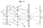
- Figure 9 is a schematic diagram illustrating the principles of the SCALPEL exposure system.
-
- Referring to Figure 1, a conventional Wehnelt electron gun assembly is shown with
base 11, cathode supportarms 12,cathode filament 13, a Wehnelt electrode including Wehnelthorizontal support arms 15 and conventionalWehnelt aperture 16. Thebase 11 may be ceramic, thesupport members 12 may be tantalum, steel, or molybdenum. Thefilament 13 may be tungsten wire, the material forming theWehnelt aperture 16 may be steel or tantalum, and theelectron emitter 14 is, e.g., a tantalum disk. The effective area of the electron emitter is typically in the range of 0.1-5.0 mm2. Theelectron emitter 14 is preferably a disk with a diameter in the range of 0.05-3.0 mm. The anode is shown schematically at 17, includinganode aperture 17a, the electron beam at 18, and a drift space at 19. For simplicity the beam control apparatus, which is conventional and well known in the art, is not shown. It will be appreciated by those skilled in the art that the dimensions in the figures are not necessarily to scale. An important feature of the electron source of SCALPEL exposure tools is relatively low electron beam brightness, as mentioned earlier. For most effective exposures, it is preferred that beam brightness be limited to a value less than 105 Acm-2sr-1. This is in contrast with conventional scanning electron beam exposure tools which are typically optimized for maximum brightness. See e.g., U.S. Patent No. 4,588,928 issued May 13, 1986 to Liu et al. - The present invention is shown in Figure 2. A
mesh grid 23 is disposed in the path of the electron emission 25 in thedrift space 19. According to Figure 2, themesh grid 23 is placed in the electrostatic field-free drift space 19, insulated from the drift tube, orliner 20, and it is biased to a specified potential Um. The potential difference between themesh grid 23 and theliner 20 creates microlenses out of each opening in themesh grid 23. Theelectron beam 18 is split into individual subbeams (beamlets), and each beamlet is focused moving through its respective mesh cell, or microlens. Themesh grid 23 is separated from theliner 20 by aninsulator 24. Themesh grid 23 and theinsulator 24 may both be part of a mesh holder. - One characteristic of the
drift space 19 is that there is substantially no or no electric field present. The substantial absence of the electric field results in no acceleration or deceleration of electrons, hence the electrons are permitted to "drift", possibly in the presence of a magnetic field. This in contrast to thevacuum gap 19a, which has a strong electric field. - Figures 2(a) and 2(b) illustrate variations on Figure 2. In particular, Figures 2(a) and 2(b) both show the
mesh grid 23 within aliner 20 attached to an electron gun assembly 1. In Figure 2(a), theliner 20 is attached to the electron gun assembly 1 via aliner flange 21 and anelectron gun flange 16. In Figure 2(b), theliner 20 is attached to the electron gun assembly 1 atweld 22. Theliner 20 and electron gun assembly 1 could be attached by other techniques known to one of ordinary skill in the art, as long as the attachment is vacuum tight. Alternatively, themesh grid 23 could be placed below the boundary between theliner flange 21 and theelectron gun flange 16 or below theweld 22, within the electron gun assembly 1, as long as themesh grid 23 remains within thedrift space 19. - One advantage of the embodiments illustrates in Figures 2(a) and 2(b) is that they permit the use of conventional non-optimal electron guns. A conventional electron gun produces a beam which is too narrow and too non-uniform. The arrangements in Figures 2(a) and 2(b) permit increased performance utilizing a conventional electron gun, since the
mesh grid 23 contained within theliner 20 improves the beam emittance by making it wider and more uniform, which is more suitable for SCALPEL applications. The effect of themesh grid 23 is more clearly illustrated in Figure 2(c). - The electron emission pattern from the Wehnelt gun of Figure 1, is shown in Figure 3. The relatively non-uniform, bell curve shaped output from the Wehnelt is evident. Figure 4 illustrates the electron beam emittance through the
mesh grid 23. The emittance on the left side of themesh grid 23 is low, whereas after passing through themesh grid 23, the emittance of the electron beam is much higher. - The screen element that forms the
mesh grid 23 can have a variety of configurations. The simplest is a conventional woven screen with square apertures. However, the screen may have triangular shaped apertures, hexagonal close packed apertures, or even circular apertures. It can be woven or non-woven. Techniques for forming suitable screens from a continuous layer may occur to those skilled in the art. For example, multiple openings in a continuous metal sheet or foil can be produced by technique such as laser drilling. Fine meshes can also be formed by electroforming techniques. Themesh grid 23 should be electrically conducting but the material of the mesh is otherwise relatively inconsequential. Tantalum, tungsten, molybdenum, titanium, or even steel are suitable materials, as are some alloys as would be known to one skilled in the art. Themesh grid 23 preferably has a transparency in the range of 40-90%, with transparency defined as the two dimensional void space divided by the overall mesh grid area. - With reference to Figure 4(a), the mesh grid has bars "b" of approximately 50 µm, and square cells with "C" approximately 200 µm. This mesh grid has a transparency of approximately 65%. Examples of mesh grid structures that were found suitable are represented by the examples in the following table.
Cell dimension "C", µm Bar width "b", µm Grid #1 200 50 Grid #2 88 37 Grid #3 54 31 - The cell dimension "C" is the width of the opening in a mesh with a square opening. For a rectangular mesh grid the dimension "C" is approximately the square root of the area of the opening. It is preferred that the openings be approximately symmetrical, i.e., square or round.
- The thickness t of the mesh grid is relatively immaterial except that the aspect ratio of the openings, C/t, is preferably greater than 1. A desirable relationship between the mesh grid parameters is given by:
- In yet another embodiment, the lens array may include more than one mesh. In one embodiment, the lens array includes three meshes. The outer two meshes may be prepared having curved shape; such a lens would provide beam emittance control and decrease spherical aberration.
- In addition the outer two meshes may also be replaced with foils, such as an SiN foil, with a thickness of approximately 0.1 µm. Such a film would permit substantially no physical interaction (inelastic collisions), and therefore a transparency approaching 100%. Due to the large current being passed through the lens array (either mesh or continuous), the transparency is important. If a high percentage of the beam impacts the structure of the mesh or continuous film, the high current is likely to melt the mesh or continuous film.
- Figure 5 is a more general representation of the optics of the present invention. 81 is the cathode of a standard high brightness electron gun, either a W hairpin, or a LaB6 crystal or a BaO gun as used in for example a CRT. 82 is the gun lens formed by the Wehnelt electrode and the extraction field. 83 is the gun cross-over with diameter dg. 84 is the electron beam emerging from the gun, with half aperture angle αg as they appear looking back from where the beam has been accelerated to 100 kV. The emittance of the gun is now
lenslets 85, thelens array 80 is positioned. Eachlenslet 85 creates animage 86 of the gun cross-over with size di. Eachsubbeam 87 now has a half opening angle α. - The emittance increase created by the
lens array 80 can be derived. Liouvilles theorem states that the particle density in six dimensional phase space cannot be changed using conservative forces such as present in lenses. This implies that the emittance within each subbeam that goes through one lenslet is conserved and thus: - The emittance of the beam appears to be
lenslets 85 and thusis the total area of the
lens array 80. The new emittance of the beam is termed the effective emittance. The emittance increase is - It is not necessary to create a real cross-over with the lenslet array. The calculation of the emittance increase then proceeds differently, but the principle still works.
- For a large emittance increase, it is beneficial to use a large pitch of the
mesh grid 23. However, the newly formed beam should include a reasonably large number of subbeams so that the subbeams will overlap at essential positions in the system such as the mask. Example 1 illustrates typical values. - A LaB6 gun of 0.2 mm diameter is used. The cross-over after the gun lens could be 60 µm, thus the emittance increase is a factor of eight using Grid #1 in Table 1.
- The
lens array 80 may be themesh grid 23 at potential V1, betweenliner 20 at potential V0 as shown in Figure 6, or include twogrids 23 and 23' at the potentials illustrated in Figure 6(a) or threegrids 23, 23', 23'' at the potentials illustrated in Figure 6(b), or any other configuration which contains a grid mesh with an electrostatic field perpendicular to the gridplane. - The focal distance of the
lenslets 85 in Figure 5 is typically in the order of 4x Vacc/Efield, where Vacc is the acceleration potential of the electron beam and Efield the strength of the electrostatic field. In Example 1, the distance between the gun cross-over and the lens array could be typically 100 mm, calling for a focal length of about 50 mm to create demagnified images. Thus, at 100 kV acceleration, the field should be 10 kV/mm. - In an alternative embodiment, if a specific configuration requires a strong field, the
mesh grid 23 could be incorporated in the acceleration unit of the gun, between the cathode and the anode. This would have the additional advantage that the beam has not yet been accelerated to the full 100 kV at that point. - In an alternative embodiment, the
mesh grid 23 could also be incorporated in the electron gun in the Wehnelt-aperture 16 of Figure 2. The mesh pitch must again be much smaller than the cathode diameter. This would lead to lenslet sizes in the order of µm's. - The present invention has been confirmed by computer simulation with both Charged Particle Optics (CPO, Bowring Consultant, Ltd., and Manchester University) and SOURCE (by MEBS, Ltd.) models. In the SOURCE model, the
mesh grid 23 is approximated by a series of circular slits. In both the CPO and SOURCE programs, a lens including two grounded cylinders with a biased mesh in the gap between those cylinders is simulated. Figure 7 shows a detail of the SOURCE model, with fields. The lensfields are clearly visible in the openings in the mesh. - Further, the modeling has been done with a three-dimensional simulation program CPO3d. Figure 8 illustrates the potential distribution in the plane of the mesh. Again, the multi-lens effect in the mesh grid can be clearly seen.
- As indicated above the electron gun of the invention is most advantageously utilized as the electron source in a SCALPEL electron beam lithography machine. Fabrication of semiconductor devices on semiconductor wafers in current industry practice contemplates the exposure of polymer resist materials with fine line patterns of actinic radiation, in this case, electron beam radiation. This is achieved in conventional practice by directing the actinic radiation through a lithographic mask and onto a resist coated substrate. The mask may be positioned close to the substrate and the image of the mask projected onto the substrate for projection printing.
- SCALPEL lithography tools are characterized by high contrast patterns at very small linewidths, i.e., 0.1 µm or less. They produce high resolution images with wide process latitude, coupled with the high throughput of optical projection systems. The high throughput is made possible by using a flood beam of electrons to expose a relatively large area of the wafer. Electron beam optics, comprising standard magnetic field beam steering and focusing, are used to image the flood beam onto the lithographic mask, and thereafter, onto the substrate, i.e., the resist coated wafer. The lithographic mask is composed of regions of high electron scattering and regions of low electron scattering, which regions define the features desired in the mask pattern. Details of suitable mask structures can be found in U.S. Patents Nos. 5,079,112 issued Jan. 7, 1992, and 5,258,246 issued Nov. 2, 1993, both to Berger et al.
- An important feature of the SCALPEL tool is the back focal plane filter that is placed between the lithographic mask and the substrate. The back focal plane filter functions by blocking the highly scattered electrons while passing the weakly scattered electrons, thus forming the image pattern on the substrate. The blocking filter thus absorbs the unwanted radiation in the image. This is in contrast to conventional lithography tools in which the unwanted radiation in the image is absorbed by the mask itself, contributing to heating and distortion of the mask, and to reduced mask lifetime.
- The principles on which SCALPEL lithography systems operate are illustrated in Figure 9.
Lithographic mask 52 is illuminated with auniform flood beam 51 of 100 keV electrons produced by the electron gun of Figure 2. Themembrane mask 52 comprisesregions 53 of high scattering material andregions 54 of low scattering material. The weakly scattered portions of the beam, i.e.,rays 51a, are focused bymagnetic lens 55 through theaperture 57 of the back focal plane blocking filter 56. The back focal plane filter 56 may be a silicon wafer or other material suitable for blocking electrons. The highly scattered portions of the electron beam, represented here byrays Regions 60 replicate thefeatures 54 of thelithographic mask 52, i.e., the regions to be exposed, andregions 61 replicate thefeatures 53 of the lithographic mask, i.e., the regions that are not to be exposed. These regions are interchangeable, as is well known in the art, to produce either negative or positive resist patterns. - A vital feature of the SCALPEL tool is the positioning of a blocking filter at or near the back focal plane of the electron beam image. Further details of SCALPEL systems can be found in U.S. Patents Nos. 5,079,112 issued Jan. 7, 1992, and 5,258,246 issued Nov. 2, 1993, both to Berger et al. These patents are incorporated herein by reference for such details that may be found useful for the practice of the invention.
- It should be understood that the figures included with his description are schematic and not necessarily to scale. Device configurations, etc., are not intended to convey any limitation on the device structures described here.
- For the purpose of definition here, and in the appended claims, the term Wehnelt emitter is intended to define a solid metal body with an approximately flat emitting surface, said flat emitting surface being symmetrical, i.e., having the shape of a circle or regular polygon. Also for the purpose of definition, the term substrate is used herein to define the object plane of the electron beam exposure system whether or not there is a semiconductor workpiece present on the substrate. The term electron optics plane may be used to describe an x-y plane in space in the electron gun and the surface onto which the electron beam image is focused, i.e., the object plane where the semiconductor wafer is situated.
- As set forth above, in the present invention, an electron optical lens array is inserted into the illumination optics of the SCALPEL tool. The position of this lens array, or fly's eye lens, is such that each lenslet creates a beam cross-over with a smaller diameter d than the distance between the lenslets L, which increases the effective emittance of the beam by a factor (L/d)2. The electron optical lens array is a mesh grid with an electrostatic field perpendicular to the grid. One advantage over conventional systems is that the present invention allows the use of a standard high brightness electron gun. Another advantage is that the effective emittance can be varied without stopping a large part of the electron current on beam shaping apertures which is now the only way to change the emittance. Yet another advantage is that a homogeneous illumination of the mask may be obtained.
Claims (29)
- A charged particle illumination system component, comprising:a lens array configured to be placed in said charged particle illumination system component.
- The charged particle illumination system component of claim 1, wherein said lens array is placed in a drift space of said charged particle illumination system component.
- The illumination system component of claim 1, wherein said illumination system component is an electron gun.
- The illumination system component of claim 1, wherein said illumination system component is a liner tube, connectable to an electron gun.
- The illumination system component of claim 4, wherein the liner tube and the electron gun are secured vacuum-tight.
- The illumination system component of claim 4, wherein the liner tube and the electron gun are bolted together.
- The illumination system component of claim 4, wherein the liner tube and the electron gun are welded together.
- The illumination system component of claim 1, said lens array including at least one mesh grid.
- The illumination system component of claim 1, said lens array including at least two mesh grids.
- The illumination system component of claim 1, said lens array including at least three mesh grids.
- The illumination system component of claim 8, said lens array further including at least one continuous foil.
- The illumination system component of claim 9, said lens array further including at least one continuous foil.
- The illumination system component of claim 1, said lens array having a transparency between 40-90%.
- A method of controlling beam emittance, comprising:placing a lens array in a charged particle illumination system component.
- The method of claim 14, wherein the lens array is placed in a drift space of the charged particle illumination system component.
- The method of claim 14, wherein the illumination system component is an electron gun.
- The method of claim 14, wherein the illumination system component is a liner tube, connectable to an electron gun.
- The method of claim 14, wherein the liner tube and the electron gun are secured vacuum-tight.
- The method of claim 14, wherein the lens array including at least one mesh grid.
- The method of claim 14, wherein the lens array including at least two mesh grids.
- The method of claim 14, wherein the lens array including at least three mesh grids.
- The method of claim 19, wherein the lens array further includes at least one continuous foil.
- The method of claim 20, wherein the lens array further includes at least one continuous foil.
- The method of claim 14, wherein the lens array has a transparency between 40-90%
- An electron beam exposure tool comprising:a charged particle illumination system component including a lens array placed in said charged particle illumination system component.
- The electron beam exposure tool of claim 25, wherein said lens array is placed in a drift space of said charged particle illumination system component.
- The electron beam exposure tool of claim 25, wherein said electron beam exposure tool is a SCALPEL tool, modified electron beam exposure system (MEBES) tool, or EBES tool.
- The electron beam exposure tool of claim 25, wherein said illumination system component is an electron gun.
- The electron beam exposure tool of claim 25, wherein said illumination system component is a liner tube, connectable to an electron gun.
Applications Claiming Priority (2)
| Application Number | Priority Date | Filing Date | Title |
|---|---|---|---|
| US09/414,004 US7345290B2 (en) | 1999-10-07 | 1999-10-07 | Lens array for electron beam lithography tool |
| US414004 | 1999-10-07 |
Publications (3)
| Publication Number | Publication Date |
|---|---|
| EP1091386A2 true EP1091386A2 (en) | 2001-04-11 |
| EP1091386A3 EP1091386A3 (en) | 2006-03-01 |
| EP1091386B1 EP1091386B1 (en) | 2012-11-21 |
Family
ID=23639556
Family Applications (1)
| Application Number | Title | Priority Date | Filing Date |
|---|---|---|---|
| EP00308685A Expired - Lifetime EP1091386B1 (en) | 1999-10-07 | 2000-10-03 | Illumination system for electron beam lithography tool |
Country Status (4)
| Country | Link |
|---|---|
| US (1) | US7345290B2 (en) |
| EP (1) | EP1091386B1 (en) |
| JP (1) | JP3895535B2 (en) |
| KR (1) | KR100757215B1 (en) |
Cited By (1)
| Publication number | Priority date | Publication date | Assignee | Title |
|---|---|---|---|---|
| EP1160824A2 (en) * | 2000-05-30 | 2001-12-05 | eLith LLC | Illumination system for charged-particle lithography apparatus |
Families Citing this family (7)
| Publication number | Priority date | Publication date | Assignee | Title |
|---|---|---|---|---|
| US7608838B1 (en) * | 2007-01-15 | 2009-10-27 | Raymond Browning | Electron optical component |
| US8084929B2 (en) * | 2009-04-29 | 2011-12-27 | Atti International Services Company, Inc. | Multiple device shaping uniform distribution of current density in electro-static focusing systems |
| EP2609611B1 (en) * | 2010-08-26 | 2017-12-20 | Tetra Laval Holdings & Finance S.A. | Control grid design for an electron beam generating device |
| US8368037B2 (en) * | 2011-03-18 | 2013-02-05 | Taiwan Semiconductor Manufacturing Company, Ltd. | Systems and methods providing electron beam writing to a medium |
| JP2013236053A (en) * | 2012-04-13 | 2013-11-21 | Canon Inc | Charged particle optical system, drawing device, and process of manufacturing article |
| US10751549B2 (en) * | 2018-07-18 | 2020-08-25 | Kenneth Hogstrom | Passive radiotherapy intensity modulator for electrons |
| US10573481B1 (en) * | 2018-11-28 | 2020-02-25 | Nuflare Technology, Inc. | Electron guns for electron beam tools |
Citations (4)
| Publication number | Priority date | Publication date | Assignee | Title |
|---|---|---|---|---|
| US5079112A (en) | 1989-08-07 | 1992-01-07 | At&T Bell Laboratories | Device manufacture involving lithographic processing |
| US5258246A (en) | 1989-08-07 | 1993-11-02 | At&T Bell Laboratories | Device manufacture involving lithographic processing |
| US5932972A (en) | 1997-02-24 | 1999-08-03 | Litton Systems, Inc. | Electron gun for a multiple beam klystron |
| EP1052677A2 (en) | 1999-05-06 | 2000-11-15 | Lucent Technologies Inc. | Electron emitters for lithography tools |
Family Cites Families (27)
| Publication number | Priority date | Publication date | Assignee | Title |
|---|---|---|---|---|
| US3107313A (en) * | 1959-10-30 | 1963-10-15 | Johann R Hechtel | Velocity modulated electron tube with cathode means providing plural electron streams |
| FR1582070A (en) * | 1968-04-26 | 1969-09-26 | ||
| US3798478A (en) * | 1972-09-14 | 1974-03-19 | Gte Sylvania Inc | Multibeam cathode ray tube having a common beam limiting aperture therein |
| US3852633A (en) * | 1972-12-13 | 1974-12-03 | Varian Associates | Gridded electron gun |
| US3886398A (en) * | 1973-08-20 | 1975-05-27 | Varian Associates | Electron beam electrical power transmission system |
| US4091311A (en) * | 1976-12-17 | 1978-05-23 | United Technologies Corporation | Modulatable, hollow beam electron gun |
| US4200794A (en) * | 1978-11-08 | 1980-04-29 | Control Data Corporation | Micro lens array and micro deflector assembly for fly's eye electron beam tubes using silicon components and techniques of fabrication and assembly |
| CH625646A5 (en) | 1979-07-06 | 1981-09-30 | Ebauches Sa | Electromagnetic motor with two directions of rotation |
| JPS5638744A (en) * | 1979-07-25 | 1981-04-14 | Hitachi Ltd | Inline electron gun structural body |
| US4338548A (en) * | 1980-01-30 | 1982-07-06 | Control Data Corporation | Unipotential lens assembly for charged particle beam tubes and method for applying correction potentials thereto |
| US4419182A (en) * | 1981-02-27 | 1983-12-06 | Veeco Instruments Inc. | Method of fabricating screen lens array plates |
| US4499405A (en) * | 1981-05-20 | 1985-02-12 | Rpc Industries | Hot cathode for broad beam electron gun |
| US4390789A (en) * | 1981-05-21 | 1983-06-28 | Control Data Corporation | Electron beam array lithography system employing multiple parallel array optics channels and method of operation |
| US4588928A (en) | 1983-06-15 | 1986-05-13 | At&T Bell Laboratories | Electron emission system |
| US4553064A (en) * | 1983-08-30 | 1985-11-12 | Hughes Aircraft Company | Dual-mode electron gun with improved shadow grid arrangement |
| JPH0789530B2 (en) | 1985-05-17 | 1995-09-27 | 日本電信電話株式会社 | Charged beam exposure device |
| CN1029055C (en) * | 1985-09-20 | 1995-06-21 | 三菱电机有限公司 | Electric gun |
| DE68917310T2 (en) * | 1989-12-13 | 1995-03-09 | Ibm | Delta-phi microlens for low energy particle beams. |
| US5260151A (en) * | 1991-12-30 | 1993-11-09 | At&T Bell Laboratories | Device manufacture involving step-and-scan delineation |
| US5376792A (en) * | 1993-04-26 | 1994-12-27 | Rj Lee Group, Inc. | Scanning electron microscope |
| JPH06338446A (en) | 1993-05-31 | 1994-12-06 | Hitachi Ltd | Charged-particle-beam aligner and drawing method using it |
| FR2733856B1 (en) * | 1995-05-05 | 1997-08-29 | Thomson Tubes Electroniques | CATHODE FOR GRID ELECTRON CANON, GRID TO BE ASSOCIATED WITH SUCH A CATHODE AND ELECTRON CANON INCLUDING SUCH CATHODE |
| US5854490A (en) * | 1995-10-03 | 1998-12-29 | Fujitsu Limited | Charged-particle-beam exposure device and charged-particle-beam exposure method |
| FR2752554B1 (en) * | 1996-08-20 | 1998-10-23 | Lohr Ind | RANCHER CARRIER WITH INTEGRATED LIFTING MEANS AND CARRIER ASSEMBLY CONSTITUTES AT LEAST ONE COUPLE OF TWO RANCHERS FUNCTIONALLY LINKED TO THEM |
| US6091187A (en) * | 1998-04-08 | 2000-07-18 | International Business Machines Corporation | High emittance electron source having high illumination uniformity |
| US6407399B1 (en) * | 1999-09-30 | 2002-06-18 | Electron Vision Corporation | Uniformity correction for large area electron source |
| US6333508B1 (en) * | 1999-10-07 | 2001-12-25 | Lucent Technologies, Inc. | Illumination system for electron beam lithography tool |
-
1999
- 1999-10-07 US US09/414,004 patent/US7345290B2/en not_active Expired - Fee Related
-
2000
- 2000-10-03 EP EP00308685A patent/EP1091386B1/en not_active Expired - Lifetime
- 2000-10-06 KR KR1020000058829A patent/KR100757215B1/en active IP Right Grant
- 2000-10-10 JP JP2000309801A patent/JP3895535B2/en not_active Expired - Fee Related
Patent Citations (4)
| Publication number | Priority date | Publication date | Assignee | Title |
|---|---|---|---|---|
| US5079112A (en) | 1989-08-07 | 1992-01-07 | At&T Bell Laboratories | Device manufacture involving lithographic processing |
| US5258246A (en) | 1989-08-07 | 1993-11-02 | At&T Bell Laboratories | Device manufacture involving lithographic processing |
| US5932972A (en) | 1997-02-24 | 1999-08-03 | Litton Systems, Inc. | Electron gun for a multiple beam klystron |
| EP1052677A2 (en) | 1999-05-06 | 2000-11-15 | Lucent Technologies Inc. | Electron emitters for lithography tools |
Non-Patent Citations (1)
| Title |
|---|
| V. KATSAP ET AL.: "Mesh-Equipped Wehnelt Source for SCALPEL", PROCEEDINGS OF SPIE, vol. 3777, July 1999 (1999-07-01), pages 75 - 81 |
Cited By (2)
| Publication number | Priority date | Publication date | Assignee | Title |
|---|---|---|---|---|
| EP1160824A2 (en) * | 2000-05-30 | 2001-12-05 | eLith LLC | Illumination system for charged-particle lithography apparatus |
| EP1160824A3 (en) * | 2000-05-30 | 2004-12-15 | eLith LLC | Illumination system for charged-particle lithography apparatus |
Also Published As
| Publication number | Publication date |
|---|---|
| JP3895535B2 (en) | 2007-03-22 |
| KR100757215B1 (en) | 2007-09-11 |
| US20030010934A1 (en) | 2003-01-16 |
| EP1091386A3 (en) | 2006-03-01 |
| JP2001229865A (en) | 2001-08-24 |
| EP1091386B1 (en) | 2012-11-21 |
| KR20010040018A (en) | 2001-05-15 |
| US7345290B2 (en) | 2008-03-18 |
Similar Documents
| Publication | Publication Date | Title |
|---|---|---|
| US6333508B1 (en) | Illumination system for electron beam lithography tool | |
| JP2002541623A (en) | Electrostatic Focused Addressable Field Emission Array Chip (AFEA's) for High Speed Massively Parallel Maskless Digital Electron Beam Direct Writing Lithography and Scanning Electron Microscopy | |
| JP2005129944A (en) | Charged-particle multibeam exposure device | |
| WO2009141428A1 (en) | Imaging system | |
| EP0958592A1 (en) | Digital direct write electron beam lithography | |
| US6232040B1 (en) | Method of electron beam exposure utilizing emitter with conductive mesh grid | |
| TW200402602A (en) | Electron beam exposure apparatus, exposure method of using electron beam, control method of electron beam, and manufacturing method of semiconductor device | |
| KR100572251B1 (en) | Apparatus and method for suppressing space charge induced aberration in charged particle projection lithography systems | |
| US6218676B1 (en) | Charged-particle-beam image-transfer apparatus exhibiting reduced space-charge effects and device fabrication methods using the same | |
| JP2002050567A (en) | Charged particle beam exposure system | |
| KR100365880B1 (en) | Shaped shadow projection for an electron beam column | |
| EP1091386B1 (en) | Illumination system for electron beam lithography tool | |
| US6091187A (en) | High emittance electron source having high illumination uniformity | |
| JPH08274020A (en) | Projective lithography device by charged particle | |
| KR100850034B1 (en) | Electron emitters for lithography tools | |
| JP3265764B2 (en) | Electron beam exposure method and apparatus | |
| JP2004228309A (en) | Method of controlling charged particle beam, method of manufacturing semiconductor device using the same, and charged particle beam exposure system using the same | |
| EP1046185A1 (en) | Projection lithography device utilizing charged particles |
Legal Events
| Date | Code | Title | Description |
|---|---|---|---|
| PUAI | Public reference made under article 153(3) epc to a published international application that has entered the european phase |
Free format text: ORIGINAL CODE: 0009012 |
|
| AK | Designated contracting states |
Kind code of ref document: A2 Designated state(s): AT BE CH CY DE DK ES FI FR GB GR IE IT LI LU MC NL PT SE |
|
| AX | Request for extension of the european patent |
Free format text: AL;LT;LV;MK;RO;SI |
|
| PUAL | Search report despatched |
Free format text: ORIGINAL CODE: 0009013 |
|
| AK | Designated contracting states |
Kind code of ref document: A3 Designated state(s): AT BE CH CY DE DK ES FI FR GB GR IE IT LI LU MC NL PT SE |
|
| AX | Request for extension of the european patent |
Extension state: AL LT LV MK RO SI |
|
| RIC1 | Information provided on ipc code assigned before grant |
Ipc: H01J 37/30 20060101ALI20060111BHEP Ipc: H01J 37/12 20060101ALI20060111BHEP Ipc: H01J 37/317 20060101ALI20060111BHEP Ipc: H01J 37/065 20060101AFI20060111BHEP |
|
| 17P | Request for examination filed |
Effective date: 20060524 |
|
| AKX | Designation fees paid |
Designated state(s): DE FR GB |
|
| 17Q | First examination report despatched |
Effective date: 20080513 |
|
| RAP3 | Party data changed (applicant data changed or rights of an application transferred) |
Owner name: LUCENT TECHNOLOGIES INC. |
|
| GRAP | Despatch of communication of intention to grant a patent |
Free format text: ORIGINAL CODE: EPIDOSNIGR1 |
|
| GRAS | Grant fee paid |
Free format text: ORIGINAL CODE: EPIDOSNIGR3 |
|
| GRAA | (expected) grant |
Free format text: ORIGINAL CODE: 0009210 |
|
| AK | Designated contracting states |
Kind code of ref document: B1 Designated state(s): DE FR GB |
|
| REG | Reference to a national code |
Ref country code: GB Ref legal event code: FG4D |
|
| REG | Reference to a national code |
Ref country code: DE Ref legal event code: R096 Ref document number: 60047649 Country of ref document: DE Effective date: 20130117 |
|
| RAP2 | Party data changed (patent owner data changed or rights of a patent transferred) |
Owner name: ALCATEL-LUCENT USA INC. |
|
| RAP2 | Party data changed (patent owner data changed or rights of a patent transferred) |
Owner name: LUCENT TECHNOLOGIES INC. |
|
| PLBE | No opposition filed within time limit |
Free format text: ORIGINAL CODE: 0009261 |
|
| STAA | Information on the status of an ep patent application or granted ep patent |
Free format text: STATUS: NO OPPOSITION FILED WITHIN TIME LIMIT |
|
| 26N | No opposition filed |
Effective date: 20130822 |
|
| REG | Reference to a national code |
Ref country code: DE Ref legal event code: R097 Ref document number: 60047649 Country of ref document: DE Effective date: 20130822 |
|
| PGFP | Annual fee paid to national office [announced via postgrant information from national office to epo] |
Ref country code: FR Payment date: 20141008 Year of fee payment: 15 |
|
| PGFP | Annual fee paid to national office [announced via postgrant information from national office to epo] |
Ref country code: GB Payment date: 20150924 Year of fee payment: 16 |
|
| REG | Reference to a national code |
Ref country code: FR Ref legal event code: ST Effective date: 20160630 |
|
| PG25 | Lapsed in a contracting state [announced via postgrant information from national office to epo] |
Ref country code: FR Free format text: LAPSE BECAUSE OF NON-PAYMENT OF DUE FEES Effective date: 20151102 |
|
| PGFP | Annual fee paid to national office [announced via postgrant information from national office to epo] |
Ref country code: DE Payment date: 20160922 Year of fee payment: 17 |
|
| GBPC | Gb: european patent ceased through non-payment of renewal fee |
Effective date: 20161003 |
|
| PG25 | Lapsed in a contracting state [announced via postgrant information from national office to epo] |
Ref country code: GB Free format text: LAPSE BECAUSE OF NON-PAYMENT OF DUE FEES Effective date: 20161003 |
|
| REG | Reference to a national code |
Ref country code: DE Ref legal event code: R119 Ref document number: 60047649 Country of ref document: DE |
|
| PG25 | Lapsed in a contracting state [announced via postgrant information from national office to epo] |
Ref country code: DE Free format text: LAPSE BECAUSE OF NON-PAYMENT OF DUE FEES Effective date: 20180501 |