BACKGROUND OF THE INVENTION
The present invention relates to a nonvolatile
flash memory in which information is rewritable by
electrical erasing/writing and a microcomputer
incorporating the same.
JP-A-1-161469 (Laid-open on June 26, 1989)
describes a microcomputer having, as a programmable
nonvolatile memory, an EPROM (erasable and programmable
read only memory) or an EEPROM (electrically erasable
and programmable read only memory) carried on a single
semiconductor chip. Data and programs are held in such
an on-chip nonvolatile memory of the microcomputer.
Since information stored in the EPROM is erased by means
of ultraviolet rays, the EPROM must be removed from a
system on which it is mounted in order for the EPROM to
be rewritten. The EEPROM can be erased and written
electrically and therefore information stored therein
can be rewritten with the EEPROM mounted on a system.
However, memory cells constituting the EEPROM must be
comprised of, in addition to memory devices such as
NMOS's (metal nitride oxide semiconductors), selecting
transistors and hence the EEPROM requires a relatively
large chip occupation area being, for example, about 2.5
to 5 times as large as that of the EPROM.
JP-A-2-289997 (Laid-open on November 29, 1990)
describes a simultaneous erasing type EEPROM. This
simultaneous erasing type EEPROM can be grasped as
having the meaning of a flash memory described in the
present specification. In the flash memory, information
can be rewritten by electrical erase and write, its
memory cell can be constructed of a single transistor as
in the EPROM and functionally, all memory cells or a
block of memory cells can be erased simultaneously by
electrical erasing. Accordingly, in the flash memory,
information stored therein can be rewritten with the
flash memory mounted on a system, the time for rewrite
can be shortened by virtue of its simultaneous erasing
function and contribution to reduction of the area
occupied by a chip can be accomplished.
U.S. Patent 5,065,364 (issued on November 12,
1991) shows a flash memory of the type in which an array
of electrically erasable and rewritable memory cells
having control gates, drains and sources is divided into
a plurality of memory blocks in a unit of data line,
source lines in common to each block are led out and a
voltage complying with an operation is applied
separately to a source line by means of a source switch
provided in each source line. At that time, ground
potential is applied to the source line of a block
selected for writing. A voltage VDI of, for example,
3.5V is applied to the source line of a block not
selected for writing. The voltage VDI guards against
word line disturbance. The word line disturbance
referred to herein is a phenomenon that for example, in
a memory cell having a word line conditioned for
selection and a data line conditioned for unselection,
the potential difference between the control gate and
floating gate is increased and as a result, electric
charge is discharged from floating gate to control gate
to decrease the threshold of the memory cell transistor.
JP-A-59-29488 (laid-open on February 16, 1991)
and JP-A-3-78195 (laid-open on April 3, 1991) describe
an ultraviolet light-erasable EPROM in which sources of
memory cells connected with the same word line are
connected in common and a source potential control
switch is provided for the commonly connected sources.
JP-A-3-78195 (laid-open on April 3, 1991) describes an
ultraviolet light-erasable EPROM in which sources of
memory cells connected with adjacent two word lines are
connected in common and a source potential control
switch is provided for each adjacent two word lines.
Each of the inventions disclosed in these three
references is intended to provide a solution to a
problem of erroneous writing/reading caused by leak
current from an unselected memory cell in an EEPROM.
Meanwhile, JP-A-3-14272 (laid-open on January
22, 1991), JP-A-3-250495 (laid-open on November 8, 1991)
and JP-A-2-241060 (laid-open on September 25, 1990)
describe division of a memory cell array in a unit to
data line.
EP-A-0 392 895 discloses a device in which selected
blocks of a flash EEPROM can be erased in parallel.
US-A-4,796,235 discloses a single chip computer including
a central processing unit, a random access memory and an
EEPROM, wherein a write protection mechanism for the EEPROM
is provided.
EP-A-0 447 856 discloses a non-volatile semiconductor
memory divided into cells and word lines to prevent non-selected
memory elements from being erroneously rewritten.
From Electronic Engineering, vol. 63, No. 775, July
1991, page 49, a flash memory having a block structure is
known which allows that the data stored in one block of the
flash memory are used as a working data set whilst a new data
set is created in a second block of the flash memory.
SUMMARY OF THE INVENTION
The object of the present invention is to provide a
semiconductor integrated circuit device having an improved
rewrite efficiency.
The object is met by the device of claim 1 which has a
control register using control bits for designating the memory
blocks to be erased. Preferred embodiments are disclosed
in the subclaims.
The present inventors have first studied the
fact that a flash memory is carried on a microcomputer
to find out the following points.
The present inventors have studied the
division of memory blocks in a unit of data line to find
that the size of the minimum memory block can be
decreased more easily by division into memory blocks in
a unit of word line and using sources in common in a
block and this is advantageous also from the standpoint
of improving ease of use of the flash memory built in
the microcomputer as studied firstly. When the division
into memory blocks in a unit of data line is employed,
all memory cells of a selected block for writing
arranged in line and having drains connected to a data
line applied with a write high voltage suffer from data
line disturbance. The data line disturbance is a
phenomenon that for example, in a memory cell associated
with a word line not rendered to be selected and a data
line rendered to be selected for writing, an electric
field between the source and drain is increased, so that
hot holes are injected from drain to floating gate to
decrease the threshold of the memory cell transistor.
A major object according to an embodiment of the invention is to provide
a microcomputer incorporating a flash memory which is
easy to use. More particularly, a first object according to an embodiment of the
invention is to provide a microcomputer capable of
making highly efficient a processing of initial write of
information into the built-in flash memory. A second
object according to an embodiment of the invention is to improve rewrite efficiency
of part of information held in some of memory blocks of
the flash memory by eliminating wastefulness of write
operation after simultaneous erasing of the memory
blocks of interest. A third object according to an embodiment of the invention is
to improve rewrite efficiency by eliminating wasteful
transfer operation, from the outside, of write
information necessary for partial rewrite of a memory
block. A fourth object according to an embodiment of the invention is to change
information held in the flash memory on real time base
in synchronism with control operation by the
microcomputer.
Further, an embodiment of the invention has for its object to
provide a flash memory in which the minimum size of
memory block obtained by using sources in common in an
electrically rewritable nonvolatile memory device can be
decreased, and to prevent an
erroneous operation due to data line disturbance in a
unselected memory block for writing from occurring when
formation of memory blocks is effected in a unit of word
line.
A microcomputer comprises,
on a single semiconductor chip, a central processing
unit and a nonvolatile flash memory in which information
to be processed by the central processing unit is
rewritable by electrical erase and write, and the
microcomputer is provided with an input terminal of an
operation mode signal for designating a first operation
mode in which rewrite of the flash memory is controlled
by a circuit built in the semiconductor chip and a
second operation mode in which it is controlled by a
unit provided externally of the semiconductor chip.
When the central processing unit performs
rewrite control in accordance with designation of the
first operation mode, a rewrite control program to be
executed by the central processing unit may be held in a
mask ROM or a rewrite control program precedently stored
in the flash memory may be transferred to a RAM and
executed.
The fact that the amount of information to be
stored in the flash memory in accordance with an
application differs in accordance with the kind of the
information such as for example a program, a data table
or control data is taken into consideration. Then, in
order that upon rewrite of part of information held in
some of memory blocks of the flash memory, efficiency of
rewrite can be improved by eliminating wastefulness of
write operation after simultaneous erasing of the memory
blocks of interest, a plurality of memory blocks having
mutually different storage capacities may be allotted
each for a simultaneously erasable unit in the flash
memory.
When rewrite of the flash memory is controlled
internally and externally of the microcomputer, in order
for a memory block to be erased simultaneously can be
designated easily, a register in which information for
designating the memory block to be erased simultaneously
is rewritably held may be incorporated in the flash
memory.
When the built-in flash memory has, as a
simultaneous erase unit, a plurality of memory blocks
having mutually different storage capacities, in order
that the built-in RAM can be utilized as a working area
or a data buffer area for rewrite of memory block, a
memory block having a storage capacity set to be smaller
than that of the built-in RAM may be provided. In this
case, for the sake of improving efficiency of rewrite by
eliminating wastefulness of transfer operation, from the
outside, of write information necessary for partial
rewrite of the memory block, information held in the
memory block having a storage capacity smaller than that
of the built-in RAM may be transferred to the built-in
RAM, all or part of the transferred information may be
renewed on the RAM and the memory block of interest may
be rewritten with renewed information. Further, upon
tuning of data such as control data held in the flash
memory, in order that information held in the flash
memory can be changed on real time base in synchronism
with control operation by the microcomputer, a
processing may be effected wherein addresses of a
specified area of the built-in RAM are controllably
changed and arranged so as to overlap addresses of the
memory block having the smaller storage capacity than
the built-in RAM, that is, changed and arranged so that
the overlapped RAM may be accessed when the memory block
is accessed and after working has been done at the
specified address, the arranged address of the RAM is
restored to the original state and the contents of the
memory block is rewritten with the information at the
specified address of the RAM.
In order to decrease the minimum block size
more easily as compared to the case where memory blocks
are formed in a unit of data line, memory blocks are
defined by connecting a common source line to memory
cells having their control gates coupled to a single or
a plurality of word lines in a unit of word line.
At that time, to take care of data line
disturbance in an unselected memory block for writing,
voltage output means is adopted which can control, in a
unit of memory block, potential of the source line to
first potential and to second potential of higher level
than that of the first potential upon write operation,
whereby the voltage output means applies the first
potential to a source line of a memory block including
memory cells having an associated data line and an
associated word line applied with predetermined voltages
so as to be selected for writing and applies the second
potential to a source line of a memory block including
memory cells having an associated data line applied with
the predetermined voltage and an associated word line
not applied with the predetermined voltage so as not to
be selected for writing.
In order to improve ease of use in the
formation of memory blocks in a unit of word line, a
plurality of memory blocks include a single or a
plurality of large memory blocks associated with a
relatively large number of word lines and a single or a
plurality of small memory blocks associated with a
relatively small number of word lines.
At that time, in order to minimize the data
line disturbance time, the large memory block and the
small memory block have data lines in common and
arranged separately in line, a selection circuit for
selecting a data line upon write and read operations is
arranged near the large memory block, a transfer gate
circuit is inserted in data lines which are associated
in common with the large memory block and small memory
block, and a control circuit is provided which cuts off
the transfer gate circuit upon write of the large memory
block.
According to the above-mentioned embodiments of
the invention, when information is initially written
into the flash memory in the phase preceding mounting of
the microcomputer according to an embodiment of the invention, the
information can be written efficiently under the control
of the external write device such as a PROM writer by
designating the second operation mode.
For example, programs, data tables or control
data are written into the plurality of memory blocks
having mutually different capacities and defined each as
a simultaneously erasable unit, in accordance with a
storage capacity of each memory block.
When the microcomputer is mounted on the
system and thereafter the flash memory is rewritten, the
first operation mode is designated to cause, for
example, the central processing unit built in the
microcomputer to execute control of rewrite. In this
case, data of a relatively large information amount can
be written in a memory block of a relatively large
storage capacity and data of a relatively small
information amount can be written in a memory block of a
relatively small storage capacity. Namely, a memory
block having a storage capacity meeting the information
amount to be stored can be utilized. Accordingly, even
when a given memory block is erased simultaneously for
rewrite of part of information held in the flash memory,
such wastefulness that an information group substantially
not required to be rewritten is erased
concurrently and thereafter written again can be
prevented as far as possible.
Especially, when of the plurality of memory
blocks, a memory block having a storage capacity set to
be smaller than that of the built-in RAM is provided,
this memory block may be utilized as a work area or a
data buffer area for rewrite of memory block. More
particularly, when the flash memory is rewritten with
the microcomputer mounted, information in a memory block
to be rewritten is transferred to the built-in RAM, only
partial information to be rewritten is received from the
outside and rewritten on the RAM and then the flash
memory is rewritten, whereby transfer, from the outside,
of information held internally in advance of rewrite and
not required to be rewritten need not be repeated, so
that wastefulness of information transfer for partial
rewrite of the memory block can be eliminated. Further,
in the flash memory, the time for simultaneously erasing
a small memory block is not so short that the flash
memory per se can be rewritten on real time base in
synchronism with control operation by the microcomputer.
But, by utilizing the built-in RAM as a work area or a
data buffer area for rewrite of memory block, the same
data as that rewritten on real time base can eventually
be obtained in the memory block.
When memory blocks are defined each in a unit
of word line, the minimum memory block has a storage
capacity which corresponds to that of one word line,
regardless of the number of parallel input/output bits.
Contrary to this, when memory blocks are defined each in
a unit of data line, the minimum memory block has a
storage capacity corresponding to the number of data
lines which in turn corresponds to the number of
parallel input/output bits. This signifies that the
storage capacity of the minimum memory block can be
reduced more easily when memory blocks are defined in a
unit of word line and especially in the case of a memory
incorporated in the microcomputer wherein input/output
of data is carried out in a unit of byte or word, the
minimum size of memory block can be reduced drastically.
This contributes to further improvement in ease of use
of the flash memory built in the microcomputer and
consequently improvement in efficiency of rewrite of
small scale data in a unit of memory block.
In a region near the source side end of the
drain of a nonvolatile memory device, electron and hole
pairs are generated owing to a tunnel phenomenon between
bands. In this case, when a relatively large electric
field is generated between the source and drain, holes
of the electron and hole pairs are accelerated by the
electric field to turn into hot holes. The hot holes
are injected to the floating gate through a tunnel
insulating film. This state is referred to as data line
disturbance and when the data line disturbance affects
the device for a long time, the threshold of the memory
device is decreased and there results an undesirable
change of stored information which leads to an erroneous
operation (data line disturbance fault). In an unselected
block for writing, by applying second potential
such as data line disturbance prevention voltage to a
source line of a memory cell to raise source potential,
an electric field between the drain and source is
weakened, thereby ensuring that holes of electron and
hole pairs generated near the drain can be prevented
from turning into hot holes to prevent a decrease in the
threshold of memory transistor.
For prevention of the data line disturbance
fault, minimization of the data line disturbance time
(the time for exposure to the data line disturbance
state) is effective. In this case, the data line
disturbance time affecting a small memory block owing to
write concomitant with rewrite of a memory block having
a large storage capacity is relatively increased in
comparison with the converse case. In view of this
fact, by adopting an arrangement in which with respect
to an intervening transfer gate circuit, memory blocks
on the side of a Y selection circuit are formed of large
memory blocks and memory blocks on the opposite side are
formed of small memory blocks, the data line disturbance
time affecting memory cells of the memory blocks
relatively near the Y selection circuit owing to write
of the memory block relatively remote from the Y selection
circuit can be reduced drastically as compared to
the case of the converse arrangement of large memory
blocks and small memory blocks. By virtue of this
arrangement relation between the large memory blocks and
small memory blocks, erroneous operation due to data
line disturbance can further be suppressed.
According to still another embodiment of the
present invention, there is provided a microcomputer
comprising a central processing unit, an electrically
rewritable flash memory, flash memory rewriting I/O port
means capable of being coupled to a ROM writer for
rewriting the flash memory, switch means located between
the central processing unit and the flash memory, and a
rewriting mode decision means responsive to an externally
supplied operation mode signal for controlling the
switch means and the flash memory rewriting I/O port
means, the central processing unit, the flash memory,
the flash memory I/O port means, the switching means and
the rewriting mode decision means being formed in a
single semiconductor chip.
According to still another embodiment of the
present invention, there is provided there is provided
an electrically rewritable flash memory device
comprising:
BRIEF DESCRIPTION OF THE DRAWINGS
Fig. 1 is a block diagram showing an
embodiment of a microcomputer adopting an all over flash
memory.
Fig. 2 is a block diagram showing an
embodiment of a microcomputer adopting a flash memory
along with a mask ROM.
Fig. 3 is a block diagram drawn from the
viewpoint of rewrite of a flash memory by means of a
general purpose PROM writer.
Fig. 4 is a block diagram drawn from the
viewpoint of rewrite of a flash memory based on CPU
control.
Fig. 5 is a memory map showing an example of a
microcomputer applied with an all over flash memory.
Fig. 6 is a memory map showing an example of a
microcomputer having a flash memory along with a mask
ROM.
Fig. 7 is a diagram for explaining an example
of the schematic control procedure of erase.
Fig. 8 is a diagram for explaining an example
of the schematic control procedure of write.
Fig. 9 is a diagram for explaining an example
of an expedient to achieve rewrite of the flash memory
on realtime base.
Fig. 10 is a diagram for explaining an example
of a manner of making partial rewrite of a memory block
of the flash memory efficient.
Figs. 11A and 11B are diagrams for explaining
the principle of the flash memory .
Fig. 12 is a diagram for explaining the
principle of construction of a memory cell array using
memory transistors of Figs. 11A and 11B.
Fig. 13 is a circuit block diagram showing an
example of a flash memory in which a plurality of memory
blocks are defined each in a unit of data line and
having different storage capacities.
Fig. 14 is a block diagram showing an
embodiment of further details of a microcomputer
corresponding to the microcomputer of Fig. 1.
Fig. 15 is a plan view showing the packaged
state of the microcomputer of Fig. 14.
Fig. 16 is a block diagram showing the whole
of the flash memory incorporated in the microcomputer of
Fig. 14.
Fig. 17 is a diagram for explaining an example
of division into memory blocks.
Fig. 18 is a diagram for explaining an example
of a control register.
Fig. 19 is a timing chart showing an example
of a memory read operation in the flash memory.
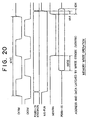
Fig. 20 is a timing chart showing an example
of a memory write operation in the flash memory.
Fig. 21 is a flow chart showing an example of
details of the write control procedure.
Fig. 22 is a flow chart showing an example of
details of the erase control procedure.
Fig. 23 is a diagram for explaining another
example of division into memory blocks.
Fig. 24 is a memory array portion configuration
diagram showing an example of a flash memory in
which a plurality of memory blocks are defined each in a
unit of word line, having different capacities.
Figs. 25A and 25B are diagrams for explaining
an advantage of the embodiment shown in Fig. 24.
Figs. 26A and 26B are diagrams for explaining
an example of voltage conditions for countermeasures
against data line disturbance in an unselected block for
writing.
Figs. 27A and 27B are diagrams for explaining
the principle of generation of data line disturbance and
countermeasures there against.
Fig. 28 is a diagram for explaining the change
of threshold of a memory cell with respect to data line
disturbance time.
Fig. 29 is a circuit diagram for explaining
the correlation of data line disturbance time between
memory blocks of small storage capacities and memory
blocks of large storage capacities.
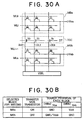
Figs. 30A and 30B are diagrams showing an
embodiment of a memory array in which a transfer gate
circuit for selectively separating data lines is
interposed between memory blocks.
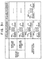
Fig. 31 in an explanatory diagram in which an
example of voltage conditions for countermeasures
against data line disturbance is summed up.
Fig. 32 is a circuit diagram showing an
example wherein a dummy word line is arranged between a
memory block and a transfer gate.
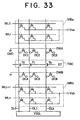
Fig. 33 is a circuit diagram showing another
example wherein a dummy word line is arranged between a
memory block and a transfer gate circuit.
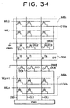
Fig. 34 is a circuit diagram showing still
another example wherein a dummy word line is arranged
between a memory block and a transfer gate circuit.
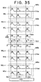
Fig. 35 is a diagram for explaining a memory
array in which two memory blocks are arranged on each
side of a transfer gate circuit.
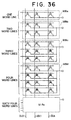
Fig. 36 is a circuit diagram showing an
example of a memory array in which the number of word
lines of simultaneously erasable memory blocks is
increased sequentially.
Fig. 37 is a diagram for explaining an example
of a memory array in which a transfer gate circuit is
arranged between a group of large memory blocks and a
group of small memory blocks.
Fig. 38 is a circuit diagram showing an
example of a memory array in which the data line
structure is constructed of main data lines and
subsidiary data lines.
Fig. 39 is a diagram for explaining an example
in which simultaneously erasable memory blocks are
arranged on the left and right sides of an X address
decoder.
Fig. 40 is a diagram for explaining an example
of a control circuit in Fig. 39.
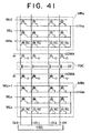
Fig. 41 is a diagram for explaining an
embodiment in which redundant words are provided in a
memory block.
Fig. 42 is a diagram for explaining an embodiment
in which memory blocks dedicated to redundancy are
provided.
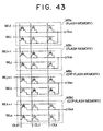
Fig. 43 is a diagram for explaining an
embodiment in which some memory blocks are formed into
one-time programmable areas.
Fig. 44 is a diagram for explaining an
embodiment in which some memory blocks are formed into
mask ROM's.
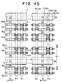
Fig. 45 is a diagram for explaining an example
of a layout pattern of memory blocks.
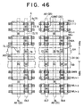
Fig. 46 is a diagram for explaining a layout
pattern in which transfer gate MOS transistors are
provided between memory blocks.
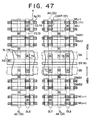
Fig. 47 is a diagram for explaining a pattern
in which the drain of a dummy cell is floating in
contrast to the configuration of Fig. 46.
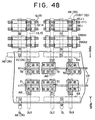
Fig. 48 is a diagram for explaining a layout
pattern in which transfer MOS transistors are
substantially increased in size.
Fig. 49 is a block diagram showing an
embodiment of the whole of a flash memory applied with
pluralization of memory blocks in a unit of word line
and countermeasures against data line disturbance.
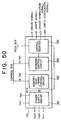
Fig. 50 is a block diagram showing details
of a control circuit included in the flash memory of
Fig. 49.
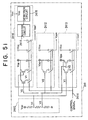
Fig. 51 is a diagram for explaining details of
a power supply circuit included in the flash memory of
Fig. 49.
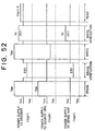
Fig. 52 is a waveform diagram showing output
voltages generated from the power supply circuit of
Fig. 51.
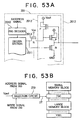
Figs. 53A and 53B are diagrams for explaining
details of an X address decoder included in the flash
memory of Fig. 49.
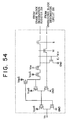
Fig. 54 is a diagram for explaining details of
an example of an erase circuit included in the flash
memory of Fig. 49.
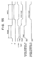
Fig. 55 is an operational timing chart of the
erase circuit of Fig. 54.
Fig. 56 is a timing chart of a series of operations
related to erase in the flash memory shown in Fig.
49.
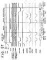
Fig. 57 is a timing chart of a series of
operations related to write in the flash memory shown in
Fig. 49.
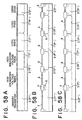
Figs. 58A to 58I are longitudinal sectional
views of a device at various stages of the production
processes of various transistors for constituting the
flash memory or the microcomputer incorporating the same.
Fig. 59 is a diagram for explaining techniques
of erasing the flash memory.
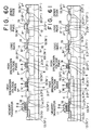
Fig. 60 is a longitudinal sectional view for
explaining a semiconductor substrate/well structure
corresponding to sector erase.
Fig. 61 is a longitudinal sectional view for
explaining another semiconductor substrate/well
structure.
Fig. 62 is a longitudinal sectional view for
explaining still another semiconductor substrate/well
structure corresponding to sector erase.
Fig. 63 is a diagram illustrating an overlap
of a specified address area of the random access memory
with a predetermined address area of the flash memory.
Fig. 64 is a diagram showing an example of a
RAM control register.
Fig. 65 is a diagram illustrating an address
setting for a specified address area of the random
access memory.
Fig. 66 is a diagram showing an example of a
chip select controller.
DESCRIPTION OF THE PREFERRED EMBODIMENTS
Embodiments of the present invention will be
described in sequence of the following items.
[1] A microcomputer adopting an allover flash memory
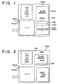
Fig. 1 is a block diagram showing an embodiment
of a microcomputer adopting an allover flash memory
(the whole of the ROM in the microcomputer being in the
form of a flash memory). In a microcomputer MCU shown
in the figure, a central processing unit CPU, a non-volatile
flash memory FMRY in which information to be
processed by the central processing unit CPU is rewritable
by electrical erase and write, peripheral
circuits such as timer TMR, serial communication
interface SCI, random access memory RAM and input/output
circuit I/O, and a control circuit CONT are formed on a
single semiconductor chip CHP such as silicon through
known semiconductor integrated circuit production
techniques. In the flash memory FMRY, information is
rewritable by electrical erase and write and like an
EPROM, its memory cell can be constructed of a single
transistor; and besides it has the function of electrically
erasing all memory cells simultaneously or a
block of memory cells (a memory block) simultaneously.
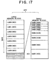
The flash memory FMRY has a plurality of memory blocks
each defined as a simultaneously erasable unit. In Fig.
1, LMB designates a large memory block having a
relatively large storage capacity and SMB represents a
small memory block having a relatively small storage
capacity. The storage memory of the small memory block
SMB is designed to be not larger than that of the random
access memory RAM. Accordingly, the random access
memory RAM can receive data transfer from the small
memory block SMB to hold the information temporarily and
can be used as a work area or data buffer area for
rewriting. Requisite data and programs are written in
the flash memory FMRY. Details of the flash memory FMRY
will be described later.
The flash memory FMRY is allowed to rewrite
its storage information under the control of the central
processing unit CPU or under the control of a unit
externally of the semiconductor chip CHP such as a
general purpose PROM writer while the microcomputer MCU
is mounted on a system. In the figure, MODE denotes an
operation mode signal for selectively designating a
first operation mode which causes the central processing
unit to control rewrite of the flash memory FMRY and a
second operation mode which causes the external unit to
control rewrite of the flash memory FRMY and the
operation mode signal is applied to a mode signal input
terminal P mode on the semiconductor chip CHP.
[2] A microcomputer adopting a mask ROM and a flash
memory
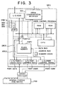
Fig. 2 is a block diagram showing an
embodiment of a microcomputer adopting a mask ROM along
with a flash memory. In microcomputer MCU shown in the
figure, part of the flash memory FMRY of Fig. 1 is
replaced with a mask read only memory MASKROM. Held in
the mask read only memory MASKROM are data and programs
which need not be rewritten. A flash memory FMRY shown
in Fig. 2 has a plurality of small memory blocks SMB
each defined as a simultaneously erasable unit.
[3] Write of information by means of a general purpose
PROM writer
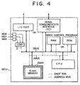
Fig. 3 is a block diagram drawn from the
viewpoint of rewrite of a flash memory FMRY by means of
a general purpose PROM writer. In the figure, as an
example of the mode signal MODE, MD0, MD1 and MD2 are
indicated. The mode signals MD0 to MD2 are supplied to
a control circuit CONT. A decoder included in the
control circuit CONT, though not limitedly, decodes the
mode signals MD0 to MD2 and decides whether an operation
mode which does not require write into the flash memory
FMRY is designated or whether the first operation mode
or the second operation mode is designated. At that
time, if designation of the second operation mode is
determined, the control circuit CONT performs control
such that it designates I/O ports which are to interface
with the general purpose PROM writer PRW and permits the
external general purpose PROM writer PRW to directly
access the built-in flash memory FMRY. More specifically,
an I/O port PORTdata for performing input/output of
data between the writer and the flash memory FMRY, an
I/O port PORTaddr for supplying address signals to the
flash memory FMRY and an I/O port PORTcont for supplying
various kinds of control signals to the flash memory
FMRY are designated. In addition, the control circuit
CONT suppresses substantial operation of built-in
function blocks having no direct relation to rewrite
control by means of the general purpose PROM writer PRW,
such as the central processing unit CPU, random access
memory RAM and mask read only memory MASKROM. For
example, connection of such a built-in function block as
the central processing unit CPU to the flash memory FMRY
is disconnected through switch means SWITCH respectively
arranged in data bus DBUS and address bus ABUS, as
exemplified in FIg. 3. The switch means SWITCH can also
be grasped as tristate type output circuits arranged in
a circuit for delivering data from the built-in function
block such as the CPU to the data bus DBUS and in a
circuit for delivering addresses to the address bus
ABUS. Such tristate output circuits are controlled such
that they are brought into high impedance condition in
response to the second operation mode. In the example
of Fig. 3, the built-in function blocks not being
directly related to the rewrite control based on the
general purpose PROM writer, such as the central
processing unit CPU, random access memory RAM and mask
read only memory MASKROM, are brought into a low power
consumption mode by a standby signal STBY* (sign* means
that a signal assigned with this sign is a low active
signal). If in a low power consumption mode the
tristate output circuits are so controlled as to be
brought into high output impedance condition, then the
power consumption mode may be set to those function
blocks in response to designation of the second
operation mode by means of the mode signals MD0 to MD2
to substantially suppress operation of the built-in
function blocks not having direct relation to the
rewrite control based on the general purpose PROM writer
PRW, such as the CPU, RAM and ROM.
When the second operation mode is set, the I/O
ports PORTdata, PORTaddr and PORTcont of the microcomputer
MCU couple to the general purpose PROM writer
PRW through a conversion socket SOCKET. The conversion
socket SOCKET has on the one hand a terminal arrangement
adapted for the I/O ports PORTdata, PORTaddr and
PORTcont and on the other hand a terminal arrangement
adapted for a standard memory, terminals of one terminal
arrangement having the same functions as those of
terminals of the other terminal arrangement being
connected mutually inside the conversion socket SOCKET.
[4] A write control program under the control of a CPU
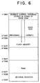
Fig. 4 is a block diagram drawn from the
viewpoint of rewrite of a flash memory based on CPU
control. In the microcomputer MCU of Fig. 1, a rewrite
control program to be executed by the central processing
unit CPU has precedently been written in the flash
memory FMRY by means of the general purpose PROM writer
PRW. In the microcomputer MCU of Fig. 2, a rewrite
control program to be executed by the central processing
unit CPU can be held in the mask read only memory
MASKROM. When the first operation mode is designated by
the mode signals MD0 to MD2 and a decoder included in
the control circuit CONT recognizes this designation,
the central processing unit CPU carries out write of
data into the flash memory FMRY in accordance with a
write control program written in the flash memory FMRY
in advance or the rewrite control program held in the
mask read only memory MASKROM.
Fig. 5 shows a memory map of the microcomputer
having the allover flash memory (see Fig. 1). In the
figure, a rewrite control program and a transfer control
program have precedently been written in predetermined
areas of the flash memory. When the first operation
mode is designated, the central processing unit CPU
executes the transfer control program to transfer the
rewrite control program to the randam access memory RAM.
After completion of the transfer, the processing of the
central processing unit CPU branches to execution of the
rewrite control program on the random access memory RAM
and through this, the erase and write (inclusive of
verification) of the flash memory FMRY is repeated.
Fig. 6 shows a memory map of the microcomputer
having the mask ROM along with the flash memory (see
Fig. 2). In this case, the transfer program as
explained with reference to Fig. 5 is unneeded. When
the first operation mode is designated, the central
processing unit CPU sequentially executes a rewrite
control program held in the mask read only memory
MASKROM to thereby repeat erase and write of the flash
memory FMRY.
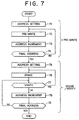
Fig. 7 shows an example of the control
procedure of erase by the central processing unit CPU.
Firstly, in accordance with the rewrite control program,
the central processing unit CPU performs pre-write of
memory cells present within an address range to be
erased (steps 71 to 74). Through this, states of the
memory cells before erase are all uniformed to written
states. Subsequently, memory cells standing for objects
to be erased are erased little by little while verifying
the degree of erase each time erase is completed
(erase/verify) in order to prevent excessive erase, thus completing
an erase operation (steps 75 to 79). Erase by
means of the general purpose PROM writer PRW can be done
in a similar way. Erase sequence for the flash memory
will be detailed hereinafter with reference to Fig. 22.
Fig. 8 shows an example of the control
procedure of write by the central processing unit CPU.
Firstly, the central processing unit CPU sets a write
start address of the flash memory FMRY (step 81).
Subsequently, data transmitted from the outside is read
through peripheral circuits designated by the rewrite
control program, for example,the serial communication
interface SCI or I/O ports (step 82). The thus read
data is written into the flash memory FMRY for a
predetermined time (step 83) and the written data is
read to verify whether the data is written normally
(write/verify) (step 84). Thereafter, the above read,
write and verify of data are repeated until they are
completed for a write end address (steps 85 and 86).
Write by means of the general purpose PROM writer can be
done in a similar way. In this case, however, data to
be written is supplied from the PROM writer PRW through
predetermined ports. Write sequence for the flash
memory will be detailed later with reference to Fig. 21.
[5] Proper use of write by the general purpose PROM
writer or write by the CPU control
Principally, write by the general purpose PROM
writer is applied to write of initial data or an initial
program used before on-board of the microcomputer MCU,
that is, mounting of the microcomputer MCU into a
system. This can ensure that a relatively large amount
of information can be written efficiently.
Write based on the CPU control is applied to
the case where tuning of data is carried out while
operating the system on which the microcomputer MCU is
mounted (called a mounting machine) or the case where
changes of data and programs under condition that the
microcomputer MCU is mounted on the system (on-board
condition), such as bug countermeasures for programs or
changes of programs concomitant with version-up of the
system, are needed. Through this, the flash memory FMRY
can be rewritten without removing the microcomputer MCU
from the mounting system.
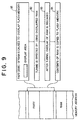
[6] Expedient to achieve rewrite on real time base
Fig. 9 shows an example of a technique of
expedient to rewrite the flash memory on real time base.
In the flash memory, because of its storage formatting,
time required for erase cannot be reduced even when the
storage capacity of a memory block defined as a simultaneous
erasing unit is made to be small and it amounts
up to, for example, several of tens of milliseconds to
several of seconds. This makes it difficult to perform
tuning of data by rewriting control data held in the
flash memory on real time base while operating the
system with the microcomputer MCU mounted thereon. To
cope with this problem, the built-in RAM is utilized as
a work area or data buffer area for rewrite of memory
block.
More particularly, data of a predetermined
small memory block SMB holding data to be subjected to
tuning is first transferred to a specified address area
of the random access memory RAM.
Next, the microcomputer MCU is switched to a
flash memory write mode of operation. This write
operation mode is set either by setting MD0 to MD2 for a
predetermined value or by setting the rewrite high
voltage Vpp to be applied to an external terminal to a
predetermined rewrite high voltage. This write mode
indicates that the flash memory FMRY is in a state in
which it can be written by the CPU and does not indicate
that the CPU is writing the flash memory.
Subsequently, a specified address area of the
random access memory RAM is overlapped with an address
of a part of the predetermined small memory block SMB of
the flash memory FMRY (step 91).
The reasons why a specified address area of
the random access memory RAM is overlapped with an
address area of a predetermined small memory block SMB
of the flash memory FMRY are as follows. Namely, when
the flash memory FMRY stores a user program (e.g., an
engine control program) and user data (e.g., engine
control data), the user data are read out by the CPU in
the course of execution of the user program to thereby
effect engine control on the basis of the read out data.
Thus, the user program contains addresses of a storage
area of the flash memory FMRY in which the user data are
stored. Therefore, in order to change the user data
(i.e., in order to effect the user data tuning) without
converting the user program, that is, without rewriting
the addresses of the user data contained in the user
program, it is necessary, for example, to change the
address location of a specified address area of the
random access memory RAM in such a manner that the
specified address area of the random access memory RAM
can be considered, when viewed in the address space of
the CPU, as being the same as a predetermined address
area of the flash memory FMRY in which the user data to
be subjected to tuning are stored.
In other words, for tuning of user data, the
addresses of the specified address area of the random
access memory RAM are changed to the addresses of an
area of the flash memory FMRY in which the user data to
be subjected to tuning are stored. When the CPU executing
the user program accesses the user data (data being
subjected to tuning) in the flash memory FMRY, actually,
the flash memory is not accessed but the specified area
of the random access memory RAM is accessed.
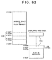
Fig. 63 is a diagrammatic representation of
overlap of the specified address area of the random
access memory RAM with the predetermined address area of
the flash memory FMRY.
For example, as shown in Fig. 63, the address
space of the flash memory FMRY is represented to be
between hexadecimal addresses E000 and EE7F, and the
address space of the random access memory RAM (built-in
RAM area) is represented to be between hexadecimal
addresses F680 and FE7F. In this figure, "H'" indicates
that the addresses are in a hexadecimal representation.
The specified address area (SRA) of the random
access memory RAM is, for example, a 128 byte-area
having addresses from H'F680 to H'F6FF. When user data
tuning is carried out, the addresses of the specified
address area (SRA) are, in Fig. 63, overlapped with
addresses H'ECOO to H'EC7E of a part of the address area
(H'ECOO to H'ECFF) of the small memory block SMB within
the address space of the flash memory FMRY.
Such a change of address arrangement can be
realized by making the decode logic of the random access
memory RAM switchable in response to a predetermined
control bit or setting of a flag.
Namely, the chip select controller CSCONT
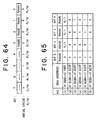
shown in Fig. 14 has a RAM control register RAMCR as
shown in Fig. 64. This register is an eight bit
register which is readable and writable from the CPU and
in which each of bits 3 to 0 has an initial value "0"
and each of the bits 7 to 4 has an initial value "1".
The bits 3 to 0 are made valid when the microcomputer
MCU is in a write operation mode. Here, the initial
values are those set in the register at the time when
the microcomputer is reset.
The bit 3 (RAMS) of the RAM control register
RAMCR determines it how the specified address area SRA
of the random access memory RAM is utilized, i.e.,
whether the specified address area SRA of the random
access memory is utilized as having its original
addresses or as having addresses overlapped with those
of a part of the address area of the small address block
SMB of the flash memory FMRY.
Fig. 65 illustrates how to set addresses of
the specified address area SRA by use of the RAM control
register RAMCR. When the RAMS bit is reset to "0", the
specified address area SRA is utilized as having its
original addresses H'F680 to H'F6FF of the random access
memory RAM, while when the RAMS bit is set to "1" with
the microcomputer CPU being under write operation mode,
the specified address area SRA is utilized as being
overlapped with the addresses of a part of the small
memory block SMB of the flash memory FMRY.
Bit 2 (RAM2) to bit 0 (RAM0) of the RAM
control register RAMCR serve to determine it where in
the small memory block SMB of the flash memory FMRY the
addresses of the specified area SRA should be overlapped
with. When the RAMS bit is reset (cleared) to "0", the
values of the bits 2 to 0 are of no significance.
Meanwhile, when the RAMS bit is set to "1", the
addresses of the specified area SRA are variable
depending on the values of the bits 2 to 0.
Namely, the addresses of the specified area
SRA are:
Then, tuning of control data is carried out
using the specified address area SRA of the random
access memory RAM which is overlapped with the address
of the predetermined memory block.
After completion of tuning (step 92), the
address overlapping of the random access memory RAM and
memory block SMB is released, so that the address
arrangement of the random access memory RAM restores its
original state (step 93). Namely, the value of the RAMS
bit of the RAM control register RAMCR is changed by the
CPU from "1" (set state) to "0" (reset or cleared
state).
Finally, data having been subjected to tuning
which is held in the the specified address area SRA of
the random access memory RAM is written by the CPU into
the predetermined address area of the memory block SMB
of the flash memory FMRY (step 94).
This writing operation is performed by
executing the write control program stored in the flash
memory FMRY. Namely, data in the small memory block of
the flash memory FMRY which data are to be changed or
tuned are erased in accordance with the steps of the
erase flow chart, as will be later described in detail
with reference to Fig. 22. Thereafter, the data having
been transferred to the random access memory RAM and
having been subjected to the tuning are written by the
CPU into the small memory block SMB of the flash memory
FMRY (the data being written in the whole of the the
small memory block SMB). In other words, the scheme
which will be next described in "[7] Making partial
rewrite of a memory block efficient" is employed.
Through this, the same data as control data
held in the flash memory which has been rewritten on
real time base can eventually be set in or obtained on
the memory block SMB while operating the system with the
microcomputer MCU mounted thereon.
Subsequently, the microcomputer MCU is
switched from the flash memory write operation mode to
the normal operation mode by resetting the mode signal
MD0 to MD2 or by resetting the rewrite high voltage Vpp
to be applied to the external terminal of the microcomputer
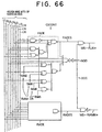
to 0 volt. Fig. 66 shows an example of a
circuit structure of a part of the chip select controller
CSCONT in which a RAM address decoder BADE and a
flash address decoder FADE are coupled to address bus
lines L15 to L7 for the higher bits 15 to 7 of the inner
address bus (bit 15 to 0) to decode the address signal
on the address bus lines L15 to L7. For example, if the
address signal on the lines L15 to L7 represents an
address area of the random access memory RAM, the RAM
address decoder RADE decodes the signal and makes its
output signal RADES high. Meanwhile, if the address
signal on the lines L15 to L7 represents an address area
of the flash memory FMRY, the flash address decoder FADE
decodes the signal and makes its output signal FADES
high.
In Fig. 66, the logic circuit OCC other than
the RAM address decoder RADE and the flash address
decoder FADE serves as means for overlapping the
addresses of the predetermined address area of the flash
memory FMRY (a part of the small memory block SMB) with
addresses of the specified address area of the random
access memory RAM, as described above. The RAMS and
RAM2 to RAM0 correspond to those of the RAM control
register RAMCR described above with reference to Fig.
64.
A specific operation of the circuit shown in
Fig. 66 is considered to be readily understood by those
skilled in the art and will not be described in detail.
With the RAMS bit value being made "1", when the
addresses of the predetermined address area of the flash
memory FMRY (the addresses overlapped with the addresses
of the specified address area SRA of the random access
memory RAM) are accessed under the conditions in which
the values of RAM2 to RAM0 are made to correspond to one
of states (2) to (6) shown in Fig. 65, a detection at a
low level indicating that the overlap designation area
is accessed appears on a point NOD in Fig. 66. As a
result, flash memory select signal MS-FLN* is brought
into a high level non-active state and RAM selection
signal MS-RAMN* is brought into a low level active state
so that the address signal for otherwise accessing the
small memory block SMB of the flash memory FMRY now
serves to access the specified address area SRA of the
random access memory RAM without accessing the small
memory block SMB of the flash memory FMRY.
On the other hand, with the RAMS bit value
being set to "1", when the address signal on the address
lines L15 to L7 indicates an address other than one of
the addresses of address areas of the flash memory FMRY
represented by bits RAM2 to RAM0 of the RAM control
register RAMCR (i.e., other than the address area of one
of the addresses represented by one of states (2) to (6)
shown in Fig. 65), the detection signal on the node NOD
is brought into a high level. As a result, when the
address signal on the address bus lines indicates the
flash memory FMRY, the flash memory selection signal MS-FLN*
is brought into a low level active state so that
data is read into the CPU from an address area of the
flash memory FMRY specified by the address signal on the
address bus lines, while when the address signal on the
address bus lines indicates the random access memory.
RAM, the RAM selection signal MS-RAMN* is brought into a
low level active state so that an address area of the
random access memory RAM specified by the address signal
on the address bus lines is accessed by the CPU for data
reading therefrom or data writing thereinto.
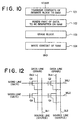
[7] Making partial rewrite of a memory block efficient
Fig. 10 shows an example of a technique of
making partial rewrite of a memory block of the flash
memory efficient. When part of information held in a
predetermined memory block of the flash memory is
rewritten upon modification of a bug of a program or
version-up of the program, information held in the
memory block having a smaller storage capacity than that
of the RAM is transferred to the built-in RAM (step
101), part of the transferred information is renewed on
the RAM (step 102), and after the data in the memory
block in question is erased (step 103), the memory block
in is rewritten with the renewed information (step 104).
Through this, even when one of the memory blocks SMB is
erased simultaneously, information held in that memory
block SMB can be preserved. Therefore, by receiving
only data to be rewritten from the outside and rewriting
the data on the RAM, transfer, from the outside, of
information not required to be rewritten and held in the
flash memory FMRY before rewriting can be unneeded, thus
avoiding wastefulness of information transfer for
partial rewrite of the memory block. The above description
with reference to Fig. 10 will be clear also from
the description with reference to Figs. 63 to 66 made
hereinbefore.
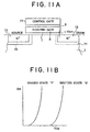
[8] The principle of the flash memory
Figs. 11A and 11B show the principle of the
flash memory. A memory cell exemplified in Fig. 11A is
constructed of an insulated gate field effect transistor
having a two-layer gate structure. In the figure, 1
designates a P type silicon substrate, 14 a P type
semiconductor region formed in the silicon substrate 1,
13 an N type semiconductor region and 15 and N type
semiconductor region of low concentration. Denoted by 8
is a floating gate formed over the P type silicon
substrate 1 through a thin oxide film 7 (for example,
having a thickness of 10 nm) serving as a tunnel
insulating film and by 11 is a control gate formed over
the floating gate 8 through an oxide film 9. A source
is formed of 13 and 15 and a drain is formed of 13 and
14. Information stored in this memory cell is substantially
held as a change in threshold voltage in the
transistor. Described hereinafter is the case where a
transistor used in the memory cell to store information
(hereinafter referred to as a memory transistor) is of N
channel type, except otherwise described.
A write operation of information to the memory
cell can be realized by, applying high voltages to, for
example, the control gate 11 and drain so that electrons
may be injected from the drain side to the floating gate
8 through avalanche injection. As a result of the write
operation, the memory transistor assumes a threshold
voltage as viewed from its control gate 7 which is
raised as shown in Fig. 11B in comparison with that of
the memory transistor without subjected to a write
operation and so placed in the erase condition.
On the other hand, an erase operation can be
realized by applying a high voltage to, for example,
the source so that electrons may be drawn out of the
floating gate 8 to the source side through tunnel
phenomenon. As a result of the erase operation, the
memory transistor assumes a threshold voltage as viewed
from its control gate 11 which is lowered as shown in
Fig. 11B. The threshold of the memory transistor shown
in Fig. 11B is set to a positive voltage level in both
of the write condition and erase condition. In other
words, in relation to a word line selection level
applied from a word line to the control gate 11, the
threshold voltage for write condition is set to be
higher and the threshold voltage for erase condition is
set to be lower. Thanks to the fact that both the
threshold voltages are related to the word line selection
level in a manner described as above, a memory cell
can be constructed of a single transistor without
employing a selection transistor. When stored information
is to be erased electrically, erase of the stored
information can be done by drawing electrons stored in
the floating gate 8 to the source electrode and therefore,
by keeping the erase operation continuing for a
relatively long time, electrons which are larger in
amount than electrons injected in the floating gate 8
upon a write operation are drawn out. Thus, when
electrical erase keeps continuing for a relatively long
time, resulting in excessive erase, the threshold
voltage of the memory transistor assumes, for example, a
negative level and there occurs such inconvenience that
a word line is selected even when the word line is at an
unselection level. Write can also be effected by
utilizing tunnel current as in the case of erase.
In a read operation, to prevent the memory
cell from being written weakly, that is, to prevent the
floating gate 8 from being injected with undesired
carriers, voltages applied to the drain and control gate
11 are limited to relatively low values. For example, a
low voltage of about 1V is applied to the drain and a
low voltage of about 5V is applied to the control gate
11. Under the application of these voltages, the
magnitude of a channel current flowing through the
memory transistor is detected so as to decide whether
information stored in the memory cell is "0" or "1".
Fig. 12 shows the principle of construction of
a memory cell array using the memory transistors. In
the figure, four memory transistors (memory cells) Q1 to
Q4 are typically depicted. In the memory cells arranged
in matrix in X and Y directions, control gates (gates
for selection of memory cells) of memory transistors Q1
and Q2 (Q3 and Q4) arranged on the same row are
connected to a corresponding word line WL1 (WL2), and
drain regions (input/output nodes of memory cells) of
memory transistors Q1 and Q3 (Q2 and Q4) are connected
to a corresponding data line DL1 (DL2). Source regions
of the memory transistors Q1 and Q3 (Q2 and Q4) are
coupled to a source line SL1 (SL2).
Table 1 shows an example of voltage conditions
for erase operation and write operations of memory
cells.
| Writing |
| memory element | selection/unselection | source | drain | gate |
| Q1 | selection | 0 V | 6 V | 12 V |
| Q2 | unselection | 0 V | 0 V | 12 V |
| Q3 | unselection | 0 V | 6 V | 0 V |
| Q4 | unselection | 0 V | 0 V | 0 V |
| Erasing (positive voltage scheme) |
| memory element | selection/unselection | source | drain | gate |
| Q1, Q3 | selection | | 12 V | 0 V | 0 V |
| Q2, Q4 | unselection | 0 V | 0 V | 0 V |
| Erasing (negative voltage scheme) |
| memory element | selection/unselection | source | drain | gate |
| Q1, Q2 | selection | | 5 V | 0 V | -10 V |
| Q3, Q4 | unselection | | 5 V | 0 V | 0 V |
In this table, memory elements mean memory cells and
gates mean control gates serving as selection gates of
the memory cells. In erase based on a negative voltage
scheme shown in the figure, a negative voltage of, for
example, -10 V is applied to the control gate to form a
high electric field necessary for erase. As is clear
from the voltage conditions exemplified in the figure,
in erase based on a positive voltage scheme, memory
cells at least sources of which are connected in common
can be erased collectively. Accordingly, with the
source lines SL1 and SL2 connected together in the
construction of Fig. 12, the four memory cells Q1 to Q4
can be erased simultaneously. In this case, by changing
the number of memory bits connected to the same source
line, the size of memory block can be set desirably. As
for the source line division scheme, in addition to a
typical instance shown in Fig. 12 where the data line is
defined as a unit (a common source line is so laid as to
extend in the data line direction), there is available
an instance where the word line is defined as a unit (a
common source line is so laid as to extend in the word
line direction). On the other hand, in erase based on
the negative voltage scheme, memory cells having control
gates connected in common can be erased simultaneously.
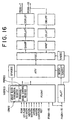
Fig. 13 is a circuit block diagram showing an
example of a flash memory in which storage capacities of
simultaneously erasable memory blocks are made to be
different.
The flash memory FMRY shown in the figure has
data input/output terminals D0 to D7 of 8 bits, so that
memory array portions ARY0 to ARY7 are provided in
association with the respective data input/output
terminals. Each of the memory array portions ARY0 to
ARY7 is divided into two of a memory block LMB having a
relatively large storage capacity and a memory block SMB
having a relatively small storage capacity. In the
figure, details of the memory array portion ARY0 are
typically illustrated and the other memory array
portions ARY1 to ARY7 are constructed similarly.
In each of the memory array portions ARY0 to
ARY7, memory cells MC formed of insulated gate field
effect transistors of two-layer gate structure as
explained previously in connection with Fig. 11 are
arranged in matrix. Also, in the figure, WL0 to WLn
designate word lines which are common to all of the
memory array portions ARY0 to ARY7. Control gates of
memory cells arranged on the same row are connected to a
corresponding word line. In each of the memory array
portions ARY0 to ARY7, drain regions of memory cells MC
arranged on the same column are connected to a corresponding
data line DL0, ... or DL7. Source regions of
memory cells MC constituting the memory block SMB are
connected in common to a source line SL1 and source
regions of memory cells MC constituting the memory block
LMB are connected in common to a source line SL2.
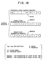
A high voltage Vpp used for erase is supplied
from voltage output circuits VOUT1 and VOUT2 to the
source lines SL1 and SL2. An output operation of the
voltage output circuits VOUT1 and VOUT2 is selected in
accordance with values of bits B1 and B2 of an erase
block designation register. For example, by setting "1"
to the bit B1 of the erase block designation register,
only the memory block SMB of each of the memory array
portions ARY0 to ARY7 is allowed to be erased simultaneously.
When "1 "is set to the bit B2 of the erase
block designation register, only the memory block LMB of
each of the memory array portions ARY0 to ARY7 is
allowed to be erased simultaneously. When "1 "is set to
both the bits B1 and B2, the whole of the flash memory
is allowed to be erased simultaneously.
Selection of the word line WL0, ... or WLn is
effected by causing a row address decoder XADEC to
decode a row address signal AX fetched in through a row
address buffer XABUFF and a row address latch XALAT. A
word driver WDRV selects a word line on the basis of a
selection signal delivered out of the row address decoder
XADEC. In a data read operation, the word driver
WDRV is operated with a power supply as represented by
voltage Vcc such as 5 V and earth potential such as 0 V
fed from a voltage selection circuit VSEL, and it drives
a word line to be selected to a selection level by the
voltage Vcc and maintains a word line not to be selected
at an unselection level such as earth potential. In a
data write operation, the word driver WDRV is operated
with a power supply as represented by voltage Vpp such
as 12 V and earth potential such as 0 V fed from the
voltage selection circuit VSEL and it drives a word line
to be selected to a write high voltage level such as 12
V. In a data erase operation, the output of the word
driver WDRV is rendered to be a low voltage level such
as 0 V.
In each of the memory array portions ARY0 to
ARY7, the data lines DL0 to DL7 are connected in common
to a common data line CD through column selection
switches YS0 to YS7. Switching control of the column
selection switches YS0 to YS7 is carried out by causing
a column address decoder YADEC to decode a column
address signal AY fetched in through a column address
buffer YABUFF and a column address latch YALAT. An
output selection signal of the column address decoder
YADEC is fed in common to all of the memory array
portions ARY0 to ARY7. Accordingly, when any one of the
output selection signals of the column address decoder
YADEC is rendered to be a selection level, a single data
line is brought into connection to the common data line
CD in each of the memory array portions ARY0 to ARY7.
Data read from a memory cell MC to the common
data line is applied to a sense amplifier SAMP through a
selection switch RS and the amplified data is delivered
to the outside through a data output latch DOLAT and a
data output buffer DOBUFF. The selection switch RS is
set to a selection level in synchronism with a read
operation. Write data fed from the outside is held in a
data input latch circuit DILAT through a data input
buffer DIBUFF. When data stored in the data input latch
circuit DILAT is "0", a write circuit WRIT supplies a
write high voltage to the common data line CD through a
selection switch WS. This write high voltage is fed to
the drain of a memory cell, whose control gate is
applied with the high voltage under the direction of a
row address signal AX, through a data line selected by a
column address signal AY, so that write into the memory
cell in question is carried out. The selection switch
WS is set to a selection level in synchronism with a
write operation. Various timings for write and erase
and voltage selection control signals are generated by a
write/erase control circuit WECONT.
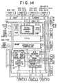
[10] Details of a microcomputer corresponding to Fig. 1
Fig. 14 is a block diagram showing an
embodiment of further details of a microcomputer
corresponding to the microcomputer of Fig. 1. The
microcomputer MCU shown in the figure comprises as the
same function blocks as those shown in Fig. 1 a central
processing unit CPU, a flash memory FMRY, a serial
communication interface SCI, a control circuit CONT and
a random access memory RAM. As equivalence to the timer
of Fig. 1, the microcomputer comprises a 16-bit
integrated timer pulse unit IPU and a watchdog timer
WDTMR. Also, as equivalence to the peripheral circuits
I/O of Fig. 1, the microcomputer comprises ports PORT1
to PORT12. Further, as the other function blocks, there
are provided a clock oscillator CPG, an interruption
controller IRCONT, an analog/digital converter ADC and a
wait state controller WSCONT. The central processing
unit CPU, flash memory FMRY, random access memory RAM
and 16-bit integrated timer pulse unit IPU are coupled
to an address bus ABUS,a lower data bus LDBUS (for
example, 8 bits) and an upper data bus HDBUS (for
example, 8 bits). The serial communication interface
SCI, watchdog timer WDTMR, interruption controller
IRCONT, analog/digital converter ADC, wait state.
controller WSCONT, chip select controller CSCONT and
ports PORT1 to PORT12 are coupled to the address bus
ABUS and higher data bus HDBUS.
In Fig. 14, the chip select controller CSCONT,
an example of a circuit structure is shown in Fig. 66,
serves as means for decoding higher bits (for example,
bits 15 to 7) of the address bus (ABUS) to generate a
selection signal indicating which address area the
address signal on the address bus (ABUS) designates for
selection. The chip select controller CSCONT may
include a plurality of address area designation
registers which are set for designating address areas of
the built-in random access memory RAM, address areas of
the built-in flash memory, address areas of I/O devices
such as a memory and/or a floppy disk controller
externally connected to the microcomputer MCU.
When the access speed of the I/O devices such
as a memory and/or a floppy disk controller externally
connected to the microcomputer is lower than the access
speed of the microcomputer, the chip select controller
CSCONT decodes the address signal on the address bus to
determine whether the address signal is for an access to
a low speed memory or an I/O device externally connected
to the microcomputer MCU. If so determined, the
chip select controller CSCONT informs the wait state
controller WSCONT thereof. As a result, the wait state
controller WSCONT inserts one or more wait states in the
bus cycle of the microcomputer. Such chip select
controller as described above is disclosed, for example,
U.S. Patent 5,070,473 issued on December 3, 1991 and
assigned to Hitachi Microcomputer Engineering Ltd. and
Hitachi, Ltd., the disclosure of which is hereby
incorporated by reference.
In Fig. 14, Vpp designates a high voltage for
rewrite of the flash memory. EXTAL and XTAL represent
signals supplied from a not-shown vibrator, provided
externally of the chip of the microcomputer, to the
clock oscillator CPG. Denoted by is a synchronizing
clock signal delivered from the clock oscillator CPG to
the outside. MD0 to MD2 designate mode signals supplied
to the control circuit CONT in order to set the first
operation mode or the second operation mode upon rewrite
of the flash memory FMRY and correspond to the mode
signal MODE in Fig. 1. Denoted by RES* is a reset
signal and by STBY* is a standby signal, these signals
being supplied to the central processing unit CPU and
other circuit blocks. NMI designates a non-maskable
interrupt signal for applying a non-maskable interruption
to the interruption controller ICONT. Other
interruption signals, not shown, are applied to the
interruption controller ICONT through the ports PORT8
and PORT9. Denoted by AS* is an address strobe signal
indicative of validity of an address signal delivered to
the outside, by RD* is a read signal for informing the
outside of a read cycle, by HWR* is an upper byte write
signal for informing the outside of a write cycle of
upper 8 bits and by LWR* is a lower byte write signal
for informing the outside of a write cycle of lower 8
bits, these signals being access control signals for the
outside of the microcomputer MCU.
The ports PORT1 and PORT2 are allotted, though
not limitedly, for input/output of data BD0 to BD15 used
for the microcomputer MCU to access the outside in the
other mode than the second operation mode in which the
external PROM writer performs direct rewrite control of
the flash memory FMRY. At that time, the ports PORT3 to
PORT 5 are allotted, though not limitedly, for address
signals BA0 to BA19.
On the other hand, when the second operation
mode is set in the microcomputer MCU, the ports PORT2 to
PORTS and PORT8 are allotted, though not limitedly, for
connection to the PROM writer adapted to control write
of the flash memory FMRY. More specifically, the port
PORT2 is allotted for input/output of data ED0 to ED7
for write and verify and the ports PORT3 to PORTS and
PORT8 are allotted for input of address signals EA0 to
EA16 as well as input of access control signal CE* (chip
enable signal), OE* (output enable signal) and WE*
(write enable signal). The chip enable signal CE* is an
operation selection signal for the flash memory FMRY
delivered from the PROM writer, the output enable signal
OE* is a designation signal of an output operation for
the flash memory FMRY and the write enable signal WE* is
a designation signal of a write operation for the flash
memory FMRY. For inputting one-bit EA9 of address
signals EA0 to EA16, the input terminal of the signal
NMI is allotted. External terminals of the thus allotted
ports and other necessary external terminals including
the application terminal of high voltage Vpp are
connected to the general purpose PROM writer through the
conversion socket SOCKET explained in connection with
Fig. 3. Conveniently, the allotment of the external
terminals at that time can be done in the form of such a
terminal arrangement that the microcomputer MCU can be
connected with ease to the PROM writer PRW through the
conversion socket SOCKET. The external terminals
allotted for connection to the PROM writer PRW in the
second operation mode are assigned with other functions
in the other operation mode of the microcomputer MCU.
Fig. 15 shows a top view of a flat package of
the Fig. 14 microcomputer MCU which is, for example,
sealed with resin and designed to have external
terminals in four directions. Signals shown in Fig. 15
are identical to those shown in Fig. 14. External
terminals (pins) not assigned with signal names may be
utilized as an input pin of a wait signal, an input pin
of a bus request signal, an output pin of a bus
acknowledge signal and input/output pins for signals
between such a peripheral circuit as serial communication
interface SCI and the outside.
In the package FP shown in Fig. 15, the
distance PP between adjacent terminals (pins) led from
the package FP may be 0.5 mm or less. To explain,
consider that a user of the microcomputer MCU connects
the flash memory FMRY included in the microcomputer MCU
to the PROM writer PRW through the conversion socket
SOCKET so as to write data into the flash memory FMRY.
In this case, when the distance between adjacent
terminals (pin pitch) PP of the package FP is set to be
0.5 mm or less, pin bends due to unwanted contact
between external terminals of the conversion socket
SOCKET and those of the package FP tend to occur when
the package FP is inserted into the conversion socket
SOCKET. In the event that such pin bends take place,
electrical connection between terminals of the conversion
socket SOCKET and those of the package FP is
prevented in respect of terminals suffering from the pin
bends, thus making it impossible to write data into the
flash memory FMRY by means of the PROM writer PRW.
As far as this point is concerned, according
to the invention, the central processing unit CPU is
allowed to write data into the flash memory FMRY and
therefore, after the package of the microcomputer MCU is
mounted on a mounting board (printed board), the user
can write data in the flash memory FMRY by means of the
central processing unit CPU without using the external
PROM writer PRW for write of data into the flash memory
FMRY, whereby even when the microcomputer MCU is sealed
in the package having the pin pitch which is 0.5 mm or
less, the user can be relieved from committing lead bends
of external terminals led from the package. It is to be
noted that in the semiconductor maker, an automatic
handler can be used and therefore a test of the microcomputer
MCU can be conducted steadily and without
causing pin bends even if the microcomputer MCU is sealed
in the package of the pin pitch being 0.5 mm or less.
[11] A control circuit for rewrite of flash memory FMRY
Fig. 16 is a block diagram showing the whole of
the flash memory FRMY incorporated in the microcomputer
MCU of Fig. 14. In the figure, ARY designates a memory
array in which memory cells formed of insulated gate
field effect transistors of two-layer gate structure
explained in connection with Figs 11A and 11B are
arranged in matrix. In this memory array ARY, like the
construction explained with reference to Fig. 13, control
gates of memory cells are connected to a corresponding
word line, drain regions of memory cells are connected to
a corresponding data line and source regions of memory
cells are connected to a source line common to each
memory block, but the array is divided into memory
blocks in a different manner from Fig. 13. For example,
as shown in Fig. 17, the array is divided into seven
large memory blocks (large blocks) LMB0 to LMB6 each
having a relatively large storage capacity and eight
small memory blocks (small blocks) SMB0 to SMB7 each
having a relatively small storage capacity.. The large
memory block is utilized as, for example, a program
storing area or a large capacity data storing area. The
small memory block is utilized as, for example, a small
capacity data storing area.
In Fig. 16, ALAT designates a latch circuit
for address signals PAB0 to PAB15. In the first operation
mode, the address signals PAB0 to PAB15 correspond
to output address signals BA0 to BA15 of the central
processing unit CPU. In the second operation mode, the
address signals PAB0 to PAB15 correspond to output
address signals EA0 to EA15 of the PROM writer PRW.
XADEC designates a row address decoder for decoding a
row address signal fetched in through the address latch
ALAT. WDRV designates a word driver for driving a word
line on the basis of a selection signal delivered out of
the row address decoder XADEC. In a data read operation,
the word driver WDRV drives the word line with a
voltage of 5 V and in a data write operation, drives the
word line with a high voltage of 12 V. In a data erase
operation, all outputs of the word driver WDRV are
rendered to be a low voltage level of 0V. YADEC
designates a column address decoder for decoding a
column address signal fetched in through the address
latch YALAT. YSEL designates a column selection circuit
for selecting a data line in accordance with an output
selection signal of the column address decoder YADEC.
SAMP designates a sense amplifier for amplifying a read
signal from a data line selected by the column selection
circuit YSEL in a data read operation. DOLAT designates
a data output latch for holding an output of the sense
amplifier. DOBUFF designates a data output buffer for
delivering data held in the data output latch DOLAT to
the outside. In the figure, PDB0 to PDB7 are data of
lower 8 bits (one byte) and PDB8 to PDB15 are data of
upper 8 bits. In accordance with this example, the
output data is of two bytes at maximum. DIBUFF
designates a data input buffer for fetching write data
fed from the outside. The data fetched in by the data
input buffer DIBUFF is held in a data input latch
circuit DILAT. When the data held in the data input
latch circuit DILAT is "0", a write circuit WRIT supplies
a write high voltage to a data line selected by
the column selection circuit YSEL. This write high
voltage is supplied to the drain of a memory cell whose
control gate is applied with a high voltage in accordance
with a row address signal, so that the memory cell
in question undergoes write. ERASEC designates an erase
circuit for supplying an erase high voltage to a source
line of a designated memory block to erase the memory
block simultaneously.
FCONT designates a control circuit for
performing timing control of a data read operation and
selection control of various timings and voltages for
write and erase. This control circuit FCONT comprises a
control register CREG including the erase block
designation register MBREG and the program/erase control
register PEREG.
Fig. 18 shows an example of the control
register CREG. The control register CREG includes a
program/erase control register PEREG of 8 bits and erase
block designation registers MBREG1 and MBREGG2 each
being of 8 bits. In the program/erase control register
PEREG, Vpp represents a high voltage applying flag which
is rendered to be "1" in accordance with the application
of a rewrite high voltage. An E bit is a bit for
designating an erase operation and an EV bit is a bit
for designating a verify operation for erasure. A P bit
is a bit for designating a write operation (program
operation) and a PV bit is a bit for designating a
verify operation for writing. The erase block
designation register MBREG1 is a register for
designating any one of memory blocks contained in the
seven divisions of large block and the erase block
designation register MBREG2 is a register for
designating any one of memory blocks contained in the
eight divisions of small block, each of these registers
having 0-th bit to seventh bit which are bits for
designating individual memory blocks whereby, for
example, bit "1" signifies selection of a corresponding
memory block and bit "0" signifies unselection of a
corresponding memory block. For example, when the
seventh bit of the erase block designation register is
"1", the small memory block SMB7 is designated.
The control register CREG is readable/writable
from the outside. The control circuit FCONT makes
reference to the contents set in the control register
CREG to control erase and write in accordance with the
contents. The operation state of erase and write can be
controlled by the CPU or externally by rewriting the
contents of the control register CREG.
In Fig. 16, the control circuit FCONT is
supplied with control signals of FLM, MS-FLM, MS-MISN,
M2RDN, M2WRN, MRDN, MWRN, IOWOTDN and RST and is also
supplied with data of PDB8 to PDB15 of upper one byte
and predetermined bits of address signals PAB0 to PAB15.
The control signal FLM is a signal for
designating an operation mode of the flash memory FMRY
whereby its "0" designates the first operation mode. and
its "1" designates the second operation mode. This
signal FLM is formed on the basis of, for example, the
mode signals MD0 to MD2.
The control signal MS-FLN is a selection
signal of the flash memory FMRY whereby its "0"
designates selection and its "1" designates unselection.
In the first operation mode, the central processing unit
CPU delivers the control signal MS-FLN and in the second
operation mode, the control signal MS-FLM corresponds to
a chip enable signal CE* supplied from the PROM writer
PRW.
The control signal MS-MISN is a selection
signal of the control register CREG. In this case,
selection of which one of the program/erase control
register PEREG, erase block designation register MBREG1
and erase block register MBREG2 is determined by
consulting predetermined bits of the address signals
PAB0 to PAB15. In the first operation mode, the central
processing unit CPU delivers the control signal MS-MISN.
In the second mode, the most significant address bit
EA16 delivered out of the PROM writer PRM is deemed as
the control signal MS-MISN, though not limitedly.
The M2RDN is a memory read strobe signal, the
M2WRN is a memory write strobe signal, the MRDN is a
read signal of the control register CREG and the MWRN is
a write signal of the control register CREG. In the
first operation mode, the central processing unit CPU
delivers these control signals. In the second operation
mode, though not limitedly, a write enable signal WE*
supplied from the PROM writer PRW is deemed as the M2WRN
and MWRN and an output enable signal OE* supplied from
the PROM writer is deemed as the M2RDN and MRDN. The
memory write strobe signal M2WRN is deemed as a strobe
signal for writing data to be written in a memory cell
into the data input latch circuit DILAT. Practically,
write into the memory cell is started by setting a P bit
of the control register CREG.
IOWORDN is a signal for switching access to
the flash memory FMRY between 8-bit read access and 16-bit
read access. In the second operation mode, this
control signal IOWORDN is fixed to a logical value for
designating the 8-bit read access.
RST is a reset signal for the flash memory
FMRY. When the flash memory FMRY is reset by this
signal RST or when the Vpp flag of program/erase control
register PEREG is rendered to be "0 ", the mode setting
bits EV, PV, E and P in the program/erase control
register PEREG are cleared.
Fig. 19 is a timing chart showing an example
of a memory read operation in the flash memory FMRY. In
the figure, CK1M and CK2M are non-overlap 2-phase clock
signals which are deemed as operation reference clock
signals. Denoted by tCYC is cycle time which differs
only slightly from access time for the RAM. A read
operation of the control register CREG is carried out at
similar timings.
Fig. 20 is a timing chart showing an example
of a memory write operation in the flash memory FMRY.
In a memory write operation designated by a write strobe
signal M2WRN shown in the figure, actual write of a
memory cell is not carried out as described previously
but input address signals PAB0 to PAB15 are held in the
address latch circuit ALAT and input data of PB8 to PB15
is held in the data input latch DILAT, thus completing a
write cycle of interest. A write operation of the
control register CREG is conducted at similar timings
but in this case, actual data write into the control
register CREG is carried out.
[12] Details of the rewrite control procedure of the
flash memory FMRY
In this item, an example of details of the
control procedure will be described in which the central
processing unit CPU or the PROM writer performs write
and erase of the flash memory through the control
circuit FCONT. Basically, in the flash memory,
information is written into a memory cell under the
erase condition. In the first operation mode in which
rewrite of the flash memory is effected with the
microcomputer mounted on the system, a rewrite control
program to be executed by the central processing unit
CPU includes a program for erase and a program for
write. The rewrite control program can be programmed
such that an erase process routine is initially executed
and a write process routine is automatically executed
without interruption in accordance with designation of
the first operation mode. Alternatively, erase and
write may be separated and then the first operation mode
may be designated thereto separately. Rewrite control
by the PROM writer can be executed through a similar
operation to that of the first operation mode. The
write control procedure and erase control procedure will
now be described.
Fig. 21 shows an example of details of the
write control procedure. The procedure shown in the
figure is the procedure for write of data of, for
example, one byte and is common to both of the control
by the central processing unit CPU in the first operation
mode and the control by the PROM writer in the
second operation mode. The following description will
be given by way of a control master which is represented
by the central processing unit CPU.
In the initial step of data write in a unit of
byte, the central processing unit CPU sets one to a
counter n built therein (step S1). Subsequently, the
central processing unit CPU performs the memory write
operation explained in connection with Fig. 20 to set
data to be written in the flash memory FMRY to the data
input latch circuit DILAT shown in Fig. 16 and set an
address to be written with the data to the address latch
circuit ALAT (step S2). Then, the central processing
unit CPU issues a write cycle to the control register
CREG to set a program bit P (step 3). Through this, the
control circuit FCONT applies, on the basis of the data
and address set in the step 2, high voltages to the
control gate and the drain of a memory cell designated
by the address to perform write. The central processing
unit CPU waits for, for example, 10 µsec. to clear the
write process time on the flash memory side (step S4)
and then clears the program bit P (step S5).
Thereafter, in order to confirm the write
state, the central processing unit CPU issues a write
cycle to the control register CREG and sets a program
verify bit PV (step 6). Through this, the control
circuit CONT utilizes the address set by the step 2 to
apply a verify voltage to a word line to be selected by
that address and to read data from the memory cell
subjected to write. To ensure a sufficient write level,
the verify level voltage is set to a voltage level of,
for example, 7 V which is higher than the power supply
voltage Vcc such as 5 V. Thus, the central processing
unit CPU checks coincidence of read-out data with data
utilized for write (step S7). If the central processing
unit CPU confirms coincidence through verify, it clears
the program verify bit PV (step S8), thus completing
write of the one-byte data.
On the other hand, if the central processing
unit CPU confirms non-coincidence through verify by step
S7, it clears the program verify bit PV in step S9 and
thereafter decides whether the value of counter n
reaches a write retry upper-limit frequency N (step
S10). Thus, if the write retry upper-limit frequency N
is reached, defective write is determined and the
processing ends. If the write retry upper-limit
frequency N is not reached, the central processing unit
CPU increments the value of counter n by one (step S11)
and repeats the processing beginning with the step S3.
Fig. 22 shows an example of details of the
erase control procedure. The procedure shown in the
figure is common to both of the control by the central
processing unit CPU in the first operation mode and the
control by the PROM writer in the second operation mode.
The following description will be given by way of a
control master which is represented by the central
processing unit CPU.
Upon erase, the central processing unit CPU
sets one to its built-in counter n (step S21).
Subsequently, the central processing unit CPU performs
pre-write of memory cells within an area to be erased
(step S22). Namely, data "0 "is written in a memory
cell at an address to be erased. The control procedure
for pre-write may make use of the write control
procedure explained with reference to Fig. 21. This
pre-write processing is carried out in order to uniform,
over all bits, electric charge amounts present in the
floating gates before erasing, thus making the erase
state uniform.
Subsequently, the central processing unit CPU
issues a write cycle to the control register CREG to
designate a memory block to be erased simultaneously
(step S23). More particularly, a memory block number to
be erased is designated to the erase block designation
registers MBREG1 and MBREG2. After the designation of
the memory block to be erased, the central processing
unit CPU issues a write cycle to the control register
CREG to set an erase bit E (step 24). Through this, the
control circuit ECONT applies a high voltage to a source
line of the memory block designated by the step 23 to
erase the memory block of interest simultaneously. The
central processing unit CPU waits for, for example, 10
msec. to clear the batch erasing process time on the
flash memory side (step S25). A time duration of 10
msec. is shorter than the time for completing one erase
operation. Then, the erase bit E is cleared (step S26).
Thereafter, in order to confirm the erase
state, the central processing unit CPU first sets
internally a head address of the memory block to be
erased simultaneously as an address to be verified (step
S27) and then performs dummy write to the verify address
(step S28). Namely, a memory write cycle is issued to
the address to be verified. Through this, the memory
address to be verified is held in the address latch
circuit ALAT. Subsequently, the central processing unit
CPU issues a write cycle to the control register CREG
and sets an erase verify bit EV (step 29). Through
this, the control circuit FCONT utilizes the address set
by the step 28 to apply an erase verify voltage to the
word line to be selected by the address and to read data
of the erased memory cell. To ensure a sufficient erase
level, the erase verify voltage is set to a voltage
level of, for example, 3.5 V which is lower than the
power supply voltage Vcc such as 5 V. Thus, the central
processing unit CPU verifies coincidence of read-out
data with data under the erase completion state (step
S30). If the central processing unit CPU confirms
coincidence through verify, it clears the erase verify
bit EV (step S31) and then decides whether the present
verify address is a final address of the erased memory
block (step S32), thus completing a series of erase
operations if the final address is identified. If the
final address is not reached, the central processing
unit CPU increments the verify address by one (step S33)
and repeats the processing beginning with the step S29.
On the other hand, if the central processing
unit CPU confirms non-coincidence through verify by step
S30, it clears the erase verify bit EV in step S34 and
thereafter decides whether the value of counter n
reaches a gradual erase upper-limit frequency N (step
S35). If the gradual erase upper-limit frequency N is
reached, a defective erase is determined and the
processing ends. If the gradual erase upper-limit is
not reached, the central processing unit CPU increments
the value of counter n by one (step S36) and repeats the
processing beginning with step S24. Practically, in
order to prevent an excessive erase in which the
threshold voltage of the memory cell assumes a negative
value owing to erase effected excessively, erase is
gradually repeated for a short time of 10msec while
performing verify every frequency.
[13] Formation of a plurality of memory blocks having
different storage capacities and defined each in a
unit of word line
Fig. 24 shows a memory mat configuration of a
flash memory in which a plurality of memory blocks are
defined each in a unit of word line and the simultaneously
erasable memory blocks have different storage
capacities.
While in the configuration shown in Fig. 13
memory blocks are defined each in a unit of data line,
memory blocks are defined in a unit of word line in Fig.
24. In the figure, a memory block LMB having a relatively
large storage capacity and a memory block SMB
having a relatively small storage capacity are illustrated
as representatives throughout memory array
portions ARY0 to ARY7.
In each of the memory array portions ARY0 to
ARY7, memory cells MC formed of insulated gate field
effect transistors of two-layer gate structure as
explained previously in connection with Fig. 11 are
arranged in matrix. In the figure, WL0 to WLn designate
word lines which are common to all of the memory array
portions ARY0 to ARY7. Control gates of memory cells
arranged on the same row are connected to a corresponding
word line. In each of the memory array
portions ARY0 to ARY7, drain regions of memory cells MC
arranged on the same column are connected to a corresponding
data line DL0, ... or DLm. Source regions
of memory cells MC constituting the small memory block
SMB are connected in common to a source line SLwi
extending in the-word line direction and source regions
of memory cells MC constituting the large memory block
LMB are connected in common to a source line SLwl
extending in the word line direction. As in the case of
Fig. 13, in simultaneous erasing effected in a unit of
memory block, a memory block to be erased simultaneously
is designated by the erase block designation register,
so that high voltage Vpp for erase is supplied to a
source line of the designated memory block. Details of
the voltage conditions for erase and write will be
described later. YSEL designates a Y selection circuit,
CD a common data line, WRIT a write circuit, DILAT a
data input latch, SAMP a sense amplifier, DOLAT a data
output latch, DIBUFF a data input buffer and DOBUFF a
data output buffer.
The relation between memory array portions
ARY0 to ARY7 and output data resembles that in Fig. 13.
More particularly, one bit of input/output data
corresponds to one memory mat. For example, data D0 is
under the charge of the memory array portion ARY0. By
employing such a configuration of one memory mat per one
input/output, the common data line CD can be sectioned,
one for each memory array portion, and need not extend
over a long distance throughout all of the memory array
portions, as illustrated in Figs. 25A and 25B. The
length of the common data line CD is much smaller than
that of the common data line CD'. Accordingly,
parasitic capacitance (Cst) associated with the common
data line CD can be reduced (Cst << C'st) to contribute
to speed-up of access and a low voltage operation.
When memory blocks such as LMB and SMB are
defined each in a unit of word line as shown in Fig. 24,
a minimum memory block in the whole of memory array ARY
having a parallel input/output bit number equal to one
byte has a storage capacity corresponding to that of one
word line, that is, the storage capacity corresponding
to the number of memory cells associated with one word
line over the entire memory array. This holds regardless
of the number of parallel input/output bits.
Contrarily, when memory blocks are defined each in unit
of data line as shown in Fig. 13, a minimum memory block
in the whole of memory array has a storage capacity
complying with the number of parallel input/output bits
to amount up to a storage capacity of 8 data lines (one
data line is associated with each memory mat). Accordingly,
if the number of memory bits in the direction of
data line is 1/8 of the number of memory bits in the
direction of word line, no difference takes place
between memory blocks defined in a unit of data line and
memory blocks defined in a unit of word line. Practically,
however, the number of memory bits in the
direction of data line is conditioned by the efficiency
of layout of semiconductor integrated circuit formation
or the efficiency of addressing memory cells, amounting
up to about 1/2 of the number of memory bits in the
direction of word line and in addition, due to the fact
that the flash memory built in the microcomputer is
connected to internal data bus, the number of parallel
input/output bits is defined in a unit of byte or word.
For these reasons, the storage capacity of the minimum
memory block can be reduced drastically in the case
where memory blocks are defined each in a unit of word
line. With the minimum size of memory block reduced,
convenience of use of a memory block as a data area can
be improved further and besides the effect of preventing
such wastefulness that information is erased simultaneously
together with information which need not substantially
be rewritten and then the latter information
is again written can fulfill itself.
[14] Countermeasures against data line disturbance in
an unselected block for writing
Figs 26A and 26B show an example of the
voltage conditions for erase/write available when memory
blocks are defined each in a unit of word line.
Especially, countermeasures against data line disturbance
are applied to an unselected block (unselected
memory block) for writing.
In Fig. 26A showing the voltage conditions for
erase, a selected block (selected memory block) 20 is a
memory block selected for simultaneous erasing and an
unselected block 21 is a memory block not selected for
simultaneous erasing. In an erase operation, word lines
WLh to WLk depicted as representatives are applied with
ground potential GND such as 0 V. In the selected block
20, its common source line SLwm is applied with a high
voltage Vpp of, for example, 12 V so that memory cells
of the selected block 20 may be erased simultaneously.
In the unselected block 21, its common source line SLwn
is maintained at ground potential GND to inhibit erase.
In Fig. 26B showing the voltage conditions for
write, a selected block 30 is a memory block containing
memory cells selected for writing and an unselected
block 31 is a memory block not containing memory cells
to be written. In the selected block 30, a common
source line SLwm is applied with ground potential GND
and when, for example, a memory cell MC circled by
phantom line is to be written, high voltage Vpp is
applied to a word line WLh connected with its control
gate and a relatively high voltage Vp of, for example, 6
V is applied to its data line. In the selected block
30, a word line WLi not selected is applied with ground
potential GND.
Upon writing, in the unselected block 31, all
word lines WLj and WLk are maintained at ground
potential GND, so that memory cells are rendered not to
be selected. Because of the nature of formation of
memory blocks in a unit of word line, the data line
extending into the unselected block 31 is also applied
with voltage Vp in accordance with write effected in the
selected block 30. Namely, a memory cell MC in the
unselected block 31 is placed in the condition of word
line unselection and data line selection in accordance
with write effected in the selected block 30. For
example, in accordance with the condition shown in Fig.
26B, when a circled memory cell in the selected block is
to be written, a memory cell (surrounded by a quadrangle
of phantom line)in the unselected block 31 and connected
to a data line DLk associated with the former memory
cell is applied with voltage Vp. Then, a common source
line SLwn in the unselected block 31 is applied with a
voltage Vddi (data line disturbance prevention voltage)
of, for example, 3.5 V to apply countermeasures against
data line disturbance. If the source line SLwn is
applied with ground potential GND as in the case of the
selected block 30, then data line disturbance will
occur. In the selected block 30, memory cells which are
connected to data line DLk and are not to be written are
applied with ground potential GND at their associated
word lines and source lines to set up the same condition
as that responsible for occurrence of data line
disturbance but such condition can be substantially
negligible. This will become apparent from item [15] of
"Correlation of data line disturbance time between
memory blocks" to be described later with reference to
Fig. 29.
Fig. 27A shows the mechanism of generation of
data line disturbance. More particularly, in a region
(1) near the source side end of drain, electron and hole
pairs are generated through a tunnel phenomenon between
bands. At that time, if the source is maintained at
ground potential GND and the drain is maintained at a
relatively high voltage Vp to generate a relatively
large electric field, holes of the electron and hole
pairs are accelerated by an electric field in a depletion
layer of the region (2) and turn into hot holes.
The hot holes pass through a thin tunnel insulating film
of about 10 nm thickness (under floating gate electrode
8) so as to be injected into the floating gate 8. This
state is a data line disturbance state and when a memory
cell transistor suffers from the data line disturbance
for a long time, its threshold is decreased, with the
result that the memory cell being in write state "0"
changes to erase state "1" and the memory cell being in
erase state "1" undergoes depletion to cause an unwanted
change of stored information or an eventual erroneous
operation (data line disturbance fault).
Fig. 27B shows the mechanism of countermeasurements
against data line disturbance. To
describe, when potential on the source side is raised in
the unselected block for writing by applying a voltage
Vddi of 3.5 V to the source of a memory cell as shown in
Figs. 26A and 26B, an electric field in a depletion
layer as indicated by a region (2) is weakened and as a
result, the turning of holes of electron and hole pairs
into hot holes is prevented to ensure that the reduction
in threshold of the memory cell transistor can be
prevented.
Fig. 28 shows an example of experiment
concerning the change of threshold of a memory cell with
respect to data line disturbance time. In this experiment,
a memory cell transistor as shown in the figure is
used and write is repeated to obtain threshold voltages
by maintaining the source potential Vs at 0 V, floating
(open) and 3.5 V, respectively, under the condition that
ground potential GND is applied to the control gate and
substrate of the memory cell transistor and 6.5 V is
applied to the drain thereof. The upper portion of the
figure is for the memory cell transistor being in the
write state "0" and the lower portion is for the memory
cell transistor being in the erase state "1". As is
clear from the figure, for Vs = 3.5 V, a decrease in
threshold which is too large to be negligible does not
occur within a data line disturbance time of about 1000
seconds under any of the erase state and the write
state.
From the above, it will be understood that in
order to prevent occurrence of faults due to data line
disturbance, the source potential of the unselected
memory block needs to be biased with a data line
disturbance prevention voltage Vddi such as 3.5 V not
higher than the drain voltage and the data line
disturbance time needs to be reduced to as small a value
as possible.
[15] Correlation of data line disturbance time between
memory blocks
The correlation of data line disturbance time
between a memory block MBa having a relatively small
storage capacity and a memory block MBb having a
relatively large storage capacity as shown in Fig. 29
will be described. For convenience of explanation, the
common source line of an unselected block for writing is
also maintained at ground potential GND as in selected
block for writing. The data line disturbance time in
this case is shown in Table 2. In this table, though
not limitedly, the write time per memory cell one bit is
set to 100 µsec. and the number of times of the erase
and write is set to 10000. One erase and write operation
referred to herein means such an operation that an
object memory block is erased simultaneously and thereafter
individual word lines are sequentially selected to
write memory cells. But the data line disturbance time
of a memory cell in the memory block selected for
writing is handled on the assumption that a word line to
which the memory cell of interest is coupled is not
selected.
| | data line disturbance time affecting MCa | data line disturbance time affecting MCb |
| MBa selected, | 〈PHASE A/A〉 | 〈PHASE B/A〉 |
| MBb unselected | 100 µS×15×1 time =1.5 msec | 100 µS×16×104 times=1.6 sec |
| MBb selected, | 〈PHASE A/B〉 | 〈PHASE B/B〉 |
| MBa unselected | 100 µS×1008×104 times=1000 sec | 100 µS×1007×1 time=0.1 sec |
| write time per bit = 100 µS |
| write/erase times = 104 |
According to the results, the data line
disturbance time affecting a memory cell MCa of the
memory block MBa is 1.5 msec when the memory block MBa
of interest is selected for writing (Phase A/A) and 1000
sec. when the memory block MBb is selected (Phase A/B).
Firstly, this difference is due to a difference in
storage capacity (the number of word lines) between the
memory blocks MBa and MBb. Namely, this is due to the
fact that while in a calculation equation of data line
disturbance time shown in Phase A/A which is 100 µs ×
15 × one frequency the time of word line switching upon
write following simultaneous erasing of the memory block
is 15 which corresponds to the number of word lines of
the memory block MBa, the number of times of word line
switching upon write following simultaneous erasing of
the memory block is 1008 corresponding to the number of
word lines of the memory block MBb in a calculation
equation of data line disturbance time shown in Phase
A/B which is 100 µs × 1008 × 10000 frequencies. Secondly,
the above difference is attributable to the fact
that in calculation of the data line disturbance time
affecting the memory cell MCa in the memory block MBa
selected for rewriting the number of times of substantial
rewrite is deemed as one. More specifically,
the difference is due to the fact while the number of
times of rewrite is deemed as one in the calculation
equation of data line disturbance time shown in Phase
A/A which is 100 µs × 15 × one time, the number of times
of rewrite is 10000 which coincides with the number of
times of actual rewrite operations in the calculation
equation of the data line disturbance time shown in
Phase A/B which is 100 µs × 1008 × 10000 times. Presumably,
this is because for the memory cell MCa in the
memory block MBa selected for rewriting, threshold
voltages of all memory cells are raised through pre-write
preceding simultaneously erasing and thereafter
erase is carried out stepwise from the viewpoint of prevention
of excessive erase upon each rewrite operation
as explained with reference to Fig. 22, so that the data
line disturbance time of the memory cell MCa of interest
is substantially defined by the time for one rewrite
operation. In other words, the data line disturbance
state affecting the memory cell MCa in the memory block
MBa selected for rewriting is deemed as being initialized
every rewrite operation. Contrary to this, when a
memory block selected for rewriting is the memory block
MBb, the memory cell MCa does not undergo the
initialization and the data line disturbance time is
accumulated in accordance with the frequency of actual
rewrite operations.
Similarly, the data line disturbance time
affecting the memory cell MCb of the memory block MBb is
0.1 sec. when the memory block MBb of interest is
selected as write object (Phase B/B) and is 16 sec. when
the memory block MBa is selected (Phase B/A). As in the
preceding, this difference is also due to the fact that
the storage capacity (the number of word lines) differs
between the memory blocks and the substantial frequency
of rewrite operations is deemed as one in the calculation
of the data line disturbance time affecting the
memory cell MCb in the memory block MBb selected for
rewriting.
From this, it is clear that the data line
disturbance time to which the unselected memory block is
subjected owing to write of the selected memory block is
far longer than the data line disturbance time affecting
the memory cell in the selected memory block. Accordingly,
it will be appreciated that in order to prevent a
decrease in threshold voltage of a memory cell due to
data line disturbance, the common source line on the
unselected memory block side for writing is at least
required to be biased by voltage Vddi but the data line
disturbance time affecting the memory cell in the
selected memory block can be neglected without causing
almost any troubles.
Further, the following will be clear from the
contents of Phase A/B and Phase B/A in the correlation
of the data line disturbance time shown in Table 2.
Namely, the data line disturbance time (e.g., 1000 sec)
affecting an unselected memory block having a small
storage capacity owing to write of a memory block having
a large capacity is relatively larger than the data line
disturbance time (e.g., 1.6 sec) in the converse case.
[16] A transfer gate circuit for data line separation
Figs. 30A and 30B show an embodiment of a
memory array in which a transfer gate circuit for
selectively separating data lines is interposed between
memory blocks. A transfer gate circuit TGC is arranged
between memory blocks MBa and MBb and has transfer MOS
transistors T0 to Tk associated with data lines DL0 to
DLk in one to one correspondence relationship, the
transfer MOS transistors being controlled for switching
by a control signal DT. According to this example, a Y
selection circuit YSEL such as a column selection switch
circuit is arranged on the side of the memory block MBb.
Fig. 30B shows switch control modes of the transfer MOS
transistors T0 to Tk. When the memory block MBa is a
selected block for writing, the transfer MOS transistors
T0 to Tk are rendered on. At that time, source
potential Vsa of the memory block MBb serving as the
selected block for writing is maintained at ground
potential GND and source potential Vsb of the memory
block MBb standing for the unselected block for writing
is maintained at data line disturbance prevention
voltage Vddi such as 3.5 V. On the other hand, when the
memory block MBb is a selected block for writing, the
transfer MOS transistors T0 to Tk are rendered off. At
that time, source potential Vsb of the memory block MBb
standing for the write selected block is maintained at
ground potential GND. Source potential Vsa of the
memory block MBa standing for an unselected block for
writing may be maintained at either data line disturbance
prevention voltage Vddi such as 3.5 V or ground
potential GND (or floating). This is because by virtue
of the transfer MOS transistors T0 to Tk rendered to be
cutoff, data line write voltage Vp fed through the Y
selection circuit YSEL is not transmitted to the memory
block MBa.
The transfer gate circuit TGC is in particular
of significance in connection with the data line
disturbance time of an unselected block for writing as
will be described below. More specifically, when the
memory block MBa is set to be a selected block for
writing, a relatively high voltage Vp for write of the
memory block MBa is applied through a data line to the
memory block MBb preceding the transfer gate circuit TGC
(on the side of Y selection circuit YSEL). Under this
condition, the common source line of the memory block
MBb serving as an unselected block for writing is
applied with data line disturbance prevention voltage
Vddi to essentially prevent data line disturbance but as
this condition continues for a long time (resulting in
considerable prolongation of the data line disturbance
time), the threshold of a memory cell subject to write
condition in the unselected memory block for writing MBb
slightly decreases even if the source of the memory cell
is biased by voltage Vddi, as will be clear from Fig.
28. Thus, by taking advantage of the fact that the data
line disturbance time affecting a memory block of a
small storage capacity owing to write concomitant with
rewrite of a memory block of a large storage capacity is
relatively larger than the data line disturbance time in
the converse case, as described with reference to Figs.
30A and 30B, the transfer gate circuit TGC intervenes
such that the memory block MBb on the side of Y selection
circuit YSEL is made to be a large memory block
having a relatively large storage capacity and the
memory block MBa on the opposite side is made to be a
small memory block having a relatively small storage
capacity. By making the memory block MBa a small memory
block and making the memory block MBb a large memory
block in this manner, the data line disturbance time
affecting a memory cell of the memory block MBb owing to
write of the memory block MBa can be far shorter than
the data line disturbance time in the case where the
memory block MBa is made to be a large memory block and
the memory block MBb is made to be a small memory block.
Through this, prevention of an erroneous operation due
to data line disturbance can further be perfected.
The countermeasures against data line
disturbance are summed up in Fig. 31. In the figure,
the voltage application condition showing countermeasures
against data line disturbance for the unselected
memory block shown at (A) is representative of
a memory cell transistor connected to a data line which
is interrupted from the supply of write voltage by the
off state of the transfer gate circuit TGC.
[17] Dummy word lines
Figs. 32, 33 and 34 are circuit diagrams in
which a dummy word line is arranged between a memory
block and a transfer gate circuit. In each of the
figures, DWA designates a dummy word line on the side of
a memory block MBa, and DWB a dummy word line on the
side of a memory block MBb. One DWA of the dummy word
lines is coupled with control gates of dummy cells DC1
to DC3 and the other DWB is coupled with control gates
of dummy cells DC4 to DC6. Each of the dummy cells DC0
to DC6 is formed of the same transistor as that of a
memory cell. In Fig. 32, the dummy cells DC0 to DC6
have their sources made to be floating and their drains
coupled to data lines. In Fig. 34, the dummy cells DC0
to DC6 have their sources and drains which are made to
be floating. In Fig. 34, the dummy cells DC0 to DC6
have their sources connected to a common source line of
a corresponding memory block and their drains made to be
floating. When a transfer gate circuit TGC is provided
between memory blocks, a repetitive pattern of memory
cell transistors and word lines is interrupted at a
position of the transfer gate circuit and from the
standpoint of device structure, there results an abrupt
unevenness in the wafer surface. Such an unevenness
leads to non-uniformity of thickness of a photoresist
film formed when word lines and control gates are formed
through, for example, photoetching. This causes partial
non-uniformity of dimensions of word lines and control
gates and irregularity in electrical characteristics of
transistors and word lines results. Under the circumstances,
by arranging the dummy word lines DWA and DWB
and the dummy cells DC0 to DC3 and DC4 to DC6 at respective
ends of the memory blocks MBa and MBb separated by
the transfer gate circuit TGC, irregularity in dimensions
of word lines and control gates which occurs near
the transfer gate circuit TGC can be reduced.
[18] Various forms of pluralization of memory blocks in
a unit of word line
As shown in Fig. 35, two memory blocks can be
arranged on each side of a transfer gate circuit TGC.
Preferably, in this case, memory blocks MBc and MBd on
the side of a Y selection circuit YAEL are made to be
large memory blocks and memory blocks MBb and MBa
succeeding the transfer gate circuit TGC are made to be
small memory blocks. For example, the large memory
block is used for program storage and the small memory
block is used for data storage.
As shown in Fig. 36, a simultaneously
erasable, minimum memory block has a single word line
and the number of word lines can be increased
sequentially to two, three and four. But the number of
word lines of individual, simultaneously erasable memory
blocks may be determined suitably or the size of
individual memory blocks may be changed suitably.
As shown in Fig. 37, when a group of
relatively small memory blocks MBa to MBe respectively
having one, two, three, four and eight word lines and a
group of relatively large memory blocks MBf each having
64 word lines are employed, a transfer gate circuit TGC
may preferably be arranged at a boundary part between
the large and small memory block groups as will be
inferred from the explanation of the previous item [16].
As shown in Fig. 38, the data line structure
is constructed of main data lines and subsidiary data
lines. Main data lines DL0 to DLk extend to reach all
memory blocks MBa to MBc. Subsidiary data lines d0 to
dk extend only inside each memory block to connect to
drains of memory cells contained in a corresponding
memory block. In this case, connection of the main data
lines DL0 to DLk to the subsidiary data lines d0 to dk
is set up through a transfer gate circuit TGC allotted
to each memory block. Such a structure can be realized
easily by, for example, a two-layer aluminum wiring
structure. Since in the main/subsidiary data line
structure the transfer gate circuit TGC is provided in
each memory block, write data line potential Vp can be
applied to only a selected block for writing.
Accordingly, counter measurements against data line
disturbance can further be perfected.
Fig. 39 shows an embodiment in which
simultaneously erasable memory blocks are arranged on
the left and right sides of an X address decoder.
Decode signals of X address decoder XADEC are delivered
to the left and right sides thereof. Then memory blocks
MBa to MBc and MBa 'to MBc' each defined in a unit of
word line arranged on each side of the X address decoder
XADEC are provided on the left and right sides thereof.
As each memory block, any one of the previously
described memory blocks can be adopted. The memory
blocks on the left and right sides perform input/output
of data io0 to io7 and data io8 to io15, respectively,
in a unit of 8 bits through Y selection circuits YSEL
and YSEL'. Transfer MOS transistors Tsw are provided
between left-hand outputs of the X address decoder XADEC
and word lines WL0 to WLn in one to one correspondence
relationship and similarly, transfer MOS transistors
Tsw' are provided between right-hand outputs of the X
address decoder XADEC and word lines WL0 'to WLn' in one
to one correspondence relationship. Further, the left-hand
word lines are associated with discharge MOS
transistors Csw and the right-hand word lines are
associated with discharge MOS transistors Csw'. A
control circuit DIVCONT is, responsive to a high voltage
Vpp1 (= Vpp such as 12V) and the most significant
address bit An, adapted to perform switching control of
the left-hand transfer MOS transistors Tsw and discharge
MOS transistors Csw and of the right-hand transfer MOS
transistors Tsw' and discharge MOS transistors Csw'.
Though not limitedly, the control circuit DIVCONT
receives a high voltage Vpp1 and the most significant
address bit An of an address signal and performs
complementary switching control between the left-hand
transfer MOS transistors Tsw and discharge MOS
transistors Csw and the right-hand transfer MOS
transistors Tsw' and discharge MOS transistors Csw' in
accordance with a logical value of the most significant
address bit An. For example, when the most significant
address bit An is logical "1", the right-hand transfer
MOS transistors Tsw' are rendered to be on and the left-hand
transfer MOS transistors Tsw are rendered to be
off, so that write data can be supplied through the
right-hand Y selection circuit YSEL'. At that time, the
right-hand discharge MOS transistors Csw' are rendered
to be off and the left-hand discharge MOS transistors
Csw are rendered to be off. When the most significant
address bit An is logical "0", the left-hand transfer
MOS transistors Tsw are rendered to be on and the right-hand
transfer MOS transistors Tsw' are rendered to be
off, so that write data is supplied through the left-hand
Y selection circuit YSEL. At that time, the right-hand
discharge MOS transistors Csw' are rendered to be
on and the left-hand discharge MOS transistors Csw are
rendered to be off. Selection operation of the left-hand
and right-hand Y selection circuits YSEL and YSEL'
depends on a decode output of a Y address decoder YADEC
but any one of the left-hand and right-hand Y selection
circuits YSEL and YSEL' may be activated by the most
significant address bit An or a signal equivalent
thereto or any one of the left-hand and right-hand Y
selection circuits may be selected as the supply path of
write data by means of a separate selection circuit not
shown. A signal voltage for rendering the transfer MOS
transistors Tsw and Tsw' on is set to a high voltage
during write and an example of the control circuit
DIVCONT for this purpose is shown in Fig. 40. A voltage
Vpp1 in Fig. 40 can be generated using a power supply
circuit of Fig. 51 to be described later.
As a comparableness to the configuration shown
in Fig. 39, a configuration may be mentioned in which an
X address decoder is arranged at one end side of word
lines. In this case, the word line direction size of a
memory block defined in a minimum unit of word line is
doubled as compared to that in Fig. 39. In comparison
with the configuration of Fig. 39, this configuration
can contribute to reduction of the word line disturbance
time of a selected block for writing. More particularly,
with reference to Fig. 26B, in the selected block 30
for writing, there is a memory cell associated with a
word line applied with high voltage Vpp and with a data
line not applied with write voltage Vp. In the selected
block 30 for writing, the memory cell placed in word
line selection condition and data line non-selection
condition suffers from a large potential difference
between the control gate and floating gate, with the
result that electric charge is discharged from the
floating gate to the control gate and the threshold of
the memory cell transistor is forced to be decreased
undesirably. This phenomenon is word line disturbance
and in proportion to prolongation of this state, the
threshold decreases. Accordingly, like the data line
disturbance, time for the word line disturbance state to
continue (word line disturbance time) is desired to be
short. From this viewpoint, the configuration of Fig.
39 is more advantageous than the comparative configuration
in that the number of memory cells exposed to the
word line disturbance state can be halved on the
presumption that write is effected in a unit of 8 bits.
This contributes to reduction of the word line
disturbance time.
Fig. 41 shows an embodiment directed to the
provision of redundant words in a memory block. In the
figure, a redundant word line WRa, a redundant data line
DR and redundant memory cells RC for relieving a defective
word line are arranged in a memory block MBa and a
redundant word line WRb, a redundant data line DR and
redundant memory cells RC for the same purpose are
arranged in a memory block MBb. With the redundant
words provided in the memory blocks MBa and MBb, when a
defective word is desired to be relieved, the defective
word can be relieved using a redundant word in the same
block as a memory block to which the defective word
belongs. For example, in the event that a word in the
memory block MBa is defective, the word can be relieved
by a redundant word WRa' in the memory block MBa of
interest. Through this, even when the defective word is
replaced with the redundant word, the counter measurements
against data line disturbance can also be applied
to the redundant word under quite the same condition.
As redundant words, memory blocks MBrd and MBrd' dedicated
to redundancy may be provided as shown in Fig. 42.
Fig. 43 shows an embodiment in which some
memory blocks are formed into one-time programmable
areas (OTP-flash). In an area formed into a one-time
programmable area, only one-time write of desired data
is allowed. In the figure, memory blocks MBc and MBd
are memory blocks which are formed into one-time
programmable areas. Structurally, the memory blocks MBc
and MBd per se which are formed into one-time
programmable areas are quite the same as the other
memory blocks. A specified memory block can be formed
into a one-time programmable area by selectively
suppressing rewrite of the memory block in question.
For example, a designation bit of an erase register for
designating a memory block which is scheduled to be
formed into a one-time programmable area is forced to
assume an unselection level by means of a nonvolatile
memory device and a path for supplying a write voltage
to a word line of the memory block of interest is so
designed as to be breakable by means of the nonvolatile
memory device. Through this, the memory block formed
into a one-time programmable area and the other memory
blocks can have in common an X address decoder, a Y
address decoder and data lines. In this case, most
conveniently, a transistor similar to a memory cell
transistor of the flash memory may be utilized as the
nonvolatile memory device. In a write operation, source
lines Vsc and Vsd of the memory blocks formed into one-time
programmable areas are applied with the data line
disturbance prevention voltage Vddi to prevent a data
line disturbance defect of these memory blocks. With
some memory blocks formed into one-time programmable
areas in this manner, occurrence of such a trouble that
data once written is subsequently rewritten undesirably
can be prevented. For example, the memory block-formed
into a one-time programmable area can be utilized as a
program holding area or a data holding area which needs
to be prevented from being altered.
Fig. 44 shows a configuration in which some
memory blocks are formed into mask ROM's, in place of
the configuration in which some memory blocks are formed
into one-time programmable areas. In the figure, memory
blocks MBc and MBd are areas which are formed into mask
ROM's. By adopting this configuration, write of the
memory blocks MBc and MBd becomes absolutely impossible.
Upon write, word lines of the memory blocks MBc and MBd
formed into mask ROM's are inhibited from being applied.
with a write high voltage and source lines Vsc and Vsd
of these memory blocks are biased by a voltage such as
Vddi. Upon erase, the common source lines Vsc and Vsd
of the memory blocks MBc and MBd are inhibited from
being applied with an erase high voltage.
[19] Layout configuration of memory blocks
Fig. 45 shows an example of a layout configuration
of memory blocks. The layout configuration shown
in the figure is an example where a transfer gate
circuit TGC is not arranged between memory blocks MBa
and MBb. In the figure, a memory cell includes a
control gate 11 integral with a word line, a floating
gate (fg) 8 formed separately from the control gate to
underlie it, a drain formed of an N type semiconductor
region 13 and a P type semiconductor region 14, and a
source formed of the N type semiconductor region 13 and
an N type semiconductor region 15. Individual memory
cells are separated from each other by a thick field
insulating film 4. Word lines WL0 to WLi+2 are
separated from each other and formed in parallel in the
lateral direction in the figure. Data lines DL0 to DL8
are formed of a first wiring layer 23 having a first
aluminum layer (A11) and are separated from each other
so as to be arranged in intersectional relation with the
word lines, thus extending in parallel in the
longitudinal direction in the figure. The data line is
connected to the drain common to an adjacent memory cell
through a contact (CONT) 22. Sources of memory cells
are each formed of the N type semiconductor regions 13
and 15 and are connected every 8 bits to a source line
SL formed of the first wiring layer 23 through the
contact 22. The source line SL is parallel to the data
lines DL0 to DL8. The source line SL in each memory
block is broken at the block end so as to be disconnected
from the source line SL of an adjacent memory
block. Contrarily to this, the data lines DL0 to DL8
extend to pass through adjacent blocks. The source line
SL in one memory block connects, at the block end, to a
common source line SA or SB formed of a second wiring
layer (A12) such as a second aluminum layer through a
through hole (TC) 25. The common source lines SA and SB
extend in parallel to the word lines to underlie the
field oxide film 4. In this manner, the source line in
a unit of memory block is provided separately. The
common source line SA or SB may be arranged at opposite
block ends or at the center of the memory block. Though
not illustrated, each word line is shunted every 16 bits
to the second wiring layer 26 overlying the word line to
reduce a delay component of the word line.
Fig. 46 shows an example of a layout configuration
in which a transfer gate circuit is provided
between memory blocks. The transfer gate circuit is
constructed by arranging transfer MOS transistors TO to
T8 each formed of a high breakdown voltage N channel
type MOS transistor having its gate electrode in the
form of a first conductive layer 8 between common source
lines SA and SB of adjacent memory blocks MBa and MBb.
In this case, data lines are broken at adjacent ends of
the memory blocks MBa and MBb. A broken end of one of
the data lines having mutually opposing broken ends is
connected to the drain of each of the transfer MOS
transistor T0 to T8 through a contact 22 and a broken
end of the other data line is connected to the source of
each of the transfer MOS transistors T0 to T7 through a
contact 22. A memory cell at an end of each of the
opposing memory blocks is used as a dummy cell having
its source being, in this example, floating. Fig. 47
shows a configuration in which the drain of a dummy cell
is floating in contrast to the configuration of Fig. 46.
Fig. 48 shows an example of a layout
configuration in which transfer MOS transistors T0 to T7
are substantially increased in size. In this example,
the gate width of each of the transfer MOS transistors
T0 to T7 is increased to prevent a decrease in data line
potential caused by each of the transfer MOS transistors
T0 to T7. More specifically, in the example of Fig. 48,
the transfer MOS transistors T0, T2, T4 and T6 are
arranged on the side of a memory block MBa in parallel
with word lines and the transfer MOS transistors T1, T3,
T5 and T7 are arranged on the side of a memory block MBb
in parallel with word lines. A data line DL0 extending
from the side of memory block MBb passes above the
transfer MOS transistor T1 so as to be coupled to the
transfer MOS transistor T0 and a data line DL0 extending
from the side of memory block MBa is coupled to the
transfer MOS transistor T0. An adjacent data line DL1
extending from the side of memory block MBa passes above
the transfer MOS transistor T0 so as to be coupled to
the transfer MOS transistor T1 and a data line DL1
extending from the side of memory block MBb is coupled
to the transfer MOS transistor T1. The other transfer
MOS transistors are also coupled to data lines in a
similar manner. The number of stacking of transfer MOS
transistors is not limited to 2 as above but can equal
the number of data lines between source lines SL at
maximum.
[20] The whole of a flash memory applied with
countermeasures against data line disturbance
Fig. 49 is a block diagram showing an embodiment
of the whole of a flash memory applied with
pluralization of memory blocks in a unit of word line
and countermeasures against data line disturbance. The
flash memory shown in the figure is incorporated in a
microcomputer. In the figure, 210 designates a memory
array in which memory cells each constructed of an
insulated gate field effect transistor of two-layer gate
structure as previously explained with reference to, for
example, Fig. 11 are arranged in matrix. In the memory
array ARY, as in the case of the configuration explained
in connection with Fig. 25, memory cells have control
gates connected to corresponding word lines, drain
regions connected to corresponding data lines and source
regions connected to source lines SL1 to SLn being each
common to respective memory blocks MB1 to MBn defined
each in a unit of word line. The source lines SL1 to
SLn of the respective memory blocks are separately
connected to erase circuits ERS1 to ERSn, respectively.
In the figure, n memory blocks MB1 to MBn are shown and
as exemplified in Fig. 18, these memory blocks may be
divided into 7 large memory blocks (large blocks) LMB0
to LMB6 each having a relatively large storage capacity
and 8 small memory blocks (small blocks) SMB0 to SMB7
each having a relatively small storage capacity. The
large memory block may be used as a program storing area
or a large capacity data storing area. The small memory
block may be used as a small capacity data storing area.
In Fig. 49, 200 designates an address buffer
and address latch circuit having its input coupled to an
internal address bus of a microcomputer. Denoted by 201
is an X address decoder (XADEC) for driving a word line
by decoding a row address signal (X address signal)
latched in the address buffer and address latch circuit
200. For example, the X address decoder 201 drives a
given word line with a voltage of, for example, 5V in a
data read operation and drives a given word line with a
high voltage of, for example, 12V in a data write
operation. In a data erase operation, all outputs of
the X address decoder 201 are maintained at a low
voltage level of, for example, 0V. Denoted by 202 is a
Y address decoder (YADEC) for decoding a Y address
signal latched in the address buffer and address latch
circuit 200. Denoted by 203 is a Y selection circuit
(YSEL) for selecting a data line in accordance with a
data line selection signal delivered out of the Y
address decoder 202. The data line is related to the Y
selection circuit such that one memory mat corresponds
to one I/O as described with reference to Fig. 25.
Though not limitedly, the memory array is divided into
16 memory mats. In this case, each of the memory blocks
MB1 to MBn extends over 16 memory mats. Denoted by 204
is a sense amplifier (SAMP) for amplifying a read signal
from a data line selected by the Y selection circuit 203
in a data read operation. According to the present
embodiment, the sense amplifier includes 16 amplifier
circuits in correspondence to output bits of the memory
mats. Denoted by 205 is a data output latch (DOLAT) for
holding an output of the sense amplifier 204. Denoted
by 206 is a data output buffer (DOBUFF) for delivering
data held in the data output latch 205 to the outside.
An output of the data output buffer 206 is coupled to a
16-bit internal data bus of the microcomputer in bit
correspondence relationship. According to this example,
read data is of 2 bytes at maximum. Denoted by 207 is a
data input buffer (DIBUFF)for fetching write data
supplied from the outside. Data fetched in from the
data input buffer 207 is held in a data input latch
(DILAT) 208. When the data held in the data input latch
208 is "0", a write circuit (WRIT) 209 supplies a write
high voltage to a data line selected by the Y selection
circuit 203. This write high voltage is supplied to the
drain of a memory cell having its control gate applied
with a high voltage in accordance with an X address
signal, causing the memory cell of interest to be
written.
Each of the erase circuits ERS1 to ERSn
supplies an erase high voltage to a source line of a
designated memory block to perform simultaneous erase of
the memory block. Which one of the erase circuits is to
be caused to effect an erase operation is controlled by
a setting bit of an erase block designation register
231. The erase block designation register 231
corresponds to the registers MBREG1 and MBREG2 explained
with reference to Fig. 18. As described with reference
to Fig. 26, the erase circuits ERS1 to ERSn are operative
upon writing to apply ground potential GND to a
source line of a selected block for writing and data
line disturbance prevention voltage Vddi to a source
line of an unselected block for writing. This control
is carried out by an unselected block designation
circuit for writing 230. The unselected block designation
circuit for writing 230 receives an X address
signal delivered out of the address buffer and address
latch circuit 200 and decodes the signal to decide a
selected block for writing, designate the application of
ground potential GND to an erase circuit associated with
the selected block for writing and designate the
application of data line disturbance prevention voltage
Vddi to an erase circuit associated with an unselected
block for writing.
In Fig. 49, 240 designates a control circuit
for performing timing control of a data read operation
and selection control of various timings and voltages
for write and erase.
Fig. 50 shows an example of the control
circuit 240. The control circuit 240 has a power supply
circuit 241, a memory read/write control circuit 242, a
register control circuit 243 and a control register 244.
The control register 244 has the program/erase control
register PEREG explained in connection with Figs. 16 and
18. The control circuit FCONT shown in Fig. 16 may be
considered to correspond to the control circuit 240 and
the erase block designation register 231 shown in Fig.
49. An erase signal E, a write signal W, an erase
verification signal EV and a write verification signal
WV correspond to an E bit, a P bit, an EV bit and a PV
bit of the program/erase control register PEREG. As
described with reference to Fig. 18, an erase/write
operation is controlled in accordance with the contents
set in the program/erase control register PEREG. On the
basis of a read/write signal R/W1 and the like supplied
through a control bus, the register control circuit 243
controls read/write of the program/erase control
register PEREG and erase block designation register 231
(MBREG1 and MBREG2) included in the control register
244. On the basis of a read/write signal R/w2 and the
like supplied through the control bus, the memory
read/write control circuit 242 controls operation of the data
input buffer 207, data input latch circuit 208, data
output buffer 206, data output latch circuit 205,
address buffer and address latch circuit 200 as well as
operation of the power supply circuit 241. The power
supply circuit 241 receives power supply voltage Vcc
such as 5V and high voltage Vpp such as 12V and forms
voltages Vpp1, VppS and Vcc1 in accordance with a setting
bit of the program/erase control register PEREG included
in the control register 244 and an output control
signal of the memory read/write control circuit 242.
Fig. 51 shows an example of a circuit diagram
of the power supply circuit 241. The power supply
circuit 241 includes a reference voltage generation
circuit 2410, a decoder drive power supply circuit 2411,
a source circuit drive power supply circuit 2412 and a
sense amplifier drive power supply circuit 2413. In the
reference voltage generation circuit 2410, a high
voltage Vpp (e.g., 12V) is divided by resistors to
generate reference voltages V1 (e.g., 3.5V) and V2
(e.g., 6.5V). In accordance with the operation state of
the flash memory the decoder drive power supply circuit
2411 generates voltage Vpp1 for determining a drive
voltage of word line. The operation state of the flash
memory is transmitted to the power supply circuit 241 by
means of a control signal 2414 from the control register
244 and memory read/write control circuit 242 so that an
internal switch circuit may be controlled to optimize
the value of voltage Vpp1 in accordance with the
operation state. An example of an output waveform of
voltage Vpp1 varying with the internal operation state
is shown in Fig. 52. The decoder drive power supply
circuit 2411 has a detection circuit 2415 for detecting
or discriminating whether the power supply voltage Vcc
has a higher voltage (e.g., 5V) or a lower voltage
(e.g., 3V) than the threshold voltage (e.g., 4V) and a
booster circuit 2416 for boosting power supply voltage
Vcc when the power supply voltage Vcc is detected as
being lower than the threshold voltage. A boosted
voltage is utilized when a read operation is effected
with the power source voltage Vcc (such as of 3V) lower
than the threshold voltage. The source circuit drive
power supply circuit 2412 generates voltage VppS
utilized for drive of source line in accordance with the
control signal 2414. The sense amplifier drive power
supply circuit 2413 generates voltage Vcc1 utilized as
drive voltage of the sense amplifier in accordance with
the control signal 2414. Voltage waveforms of voltages
VppS and Vcc1 varying with the internal state of the
flash memory are depicted in Fig. 52.
Fig. 53A shows an example of the X address
decoder 201. In the figure, the construction
corresponding to one word line is typically illustrated.
The X address decoder consists of a pre-decoder 2010 for
receiving an X address signal, a decode section 2011 for
decoding an output of the pre-decoder and a drive
section 2011 for driving a word line on the basis of an
output of the decode section 2011. The pre-decoder 2010
and decode section 2011 are operated with a power supply
voltage Vcc such as 5V system. The drive section 2012
is constructed as a high voltage driven system which is
driven by a voltage such as the voltage Vpp1. Denoted
by 2013 is a high breakdown voltage N channel type MOS
transistor for separating the 5V system from the high
voltage system.
When the transfer gate circuit TGC as
described with reference to Figs. 32 to 35 is adopted,
the large memory blocks LMB0 to LMB6 shown in Fig. 16
correspond to memory blocks MB1 to MB7 of Fig. 49 and
the small memory blocks SMB0 to SMB7 correspond to
memory blocks MB8 to MBn of Fig. 49. In Fig. 49, the
transfer gate circuit TGC is arranged between the memory
blocks MB7 and MB8, though not illustrated particularly.
Fig. 53B shows an example of a selection circuit 250 for
generating a switching signal DT of the transfer gate
circuit TGC. The selection circuit 250 receives the
voltage Vpp1 from the power supply circuit 241, address
signal from the address buffer 20B and write signal from
the control circuit 240 to cut off the transfer gate
circuit TGC upon write of the large memory blocks. In
particular, the signal DT is set to 0V corresponding to
ground potential upon write of the large memory block
but in the other case, set to voltage Vpp1, though not
limitedly.
Fig. 54 shows an example of the erase circuit
and Fig. 55 shows its operational timing chart.
Supplied to each of the erase circuits ERS1 to ERSn is
operating voltage represented by the voltage VppS and
power supply voltage Vdd. Signal E/W* shown in the
figure is a signal which is maintained at 0 level upon
write or erase. When a bit supplied from the erase
block designation register to the erase circuit of Fig.
54 is "1" level (erase designating level), erase signal
E from the control circuit 240 is also rendered to be
"1" level and supply voltage Vs to a source line is set
to the voltage VppS. Voltage Vpps upon erase is set to
Vpp as described with reference to Fig. 52. Through
this, in a selected block for simultaneous erasing,
simultaneous erase of memory cells can be done. When a
control signal supplied from the upon-write unselected
block designation circuit to the erase circuit of Fig.
54 is "1" level (level for designating an unselected
block) for writing, write signal W from the control
circuit 240 is also rendered to be "1" level and supply
voltage Vs to the source line is set to the voltage
VppS. Voltage VppS upon write is maintained at data
line disturbance prevention voltage Vddi such as 3.5V.
Through this, data line disturbance can be prevented in
the unselected block for writing.
Fig. 56 shows a timing chart of a series of
operations related to erase in the flash memory shown in
Fig. 49 and Fig. 57 shows a timing chart of a series of
operations related to write in the flash memory shown in
Fig. 49. Prior to giving a description of each timing
chart, control signals shown in these figures will first
be described. Part of the contents of the description
given in connection with Fig. 16 will be repeated herein
because this is considered to be necessary for
facilitating understanding. Control signal FLM is a
signal for designating the operation mode of the flash
memory FMRY, whereby its "0" designates the first operation
mode and its "1" designates the second operation
mode. This signal FLM is formed on the basis of, for
example, the mode signals MD0 to MD2. Control signal
MS-MiSN is a selection signal of the flash memory FMRY,
whereby its "0" designates selection and its "1"
designates unselection. Control signal MS-MISN is a
selection signal of internal registers such as the
program/erase control register PEREG and erase block
designation registers MBREG1 and MBREG2. Which one of
the registers is to be selected is determined by an
address signal PABm. Denoted by M2RDN is a memory read
strobe signal, by M2WRN is a memory write strobe signal,
by MRDN is a read signal of registers built in the flash
memory and MWRN is a write signal of registers built in
the flash memory. The memory write strobe signal M2WRN
is deemed as a strobe signal for writing data to be
written in a memory cell into the data input latch
DILAT. Actual write to the memory cell is started by
setting a P bit of the program/erase control register
PEREG.
A series of operations related to erase are
mainly sorted into a setup erase, an erase and an erase
verify as shown in Fig. 56. The setup erase consists of
an operation of writing data for designation of a memory
block to be erased simultaneously into the erase block
designation register and an operation of writing a bit
(flag) of logic "1" into an E bit of the program/erase
control register PEREG. The erase is an operation of
erasing a memory block simultaneously and is started by
setting "1" in the E bit. The specific processing
procedure of an erase operation is the same as the
contents explained in connection with Fig. 22. The
erase verify is started by clearing the E bit so that
verify may be carried out sequentially in a unit of
byte, beginning with a head address, in accordance with
the contents explained in connection with Fig. 22.
As shown in Fig. 57, a series of operations
related to write are mainly sorted into a setup program,
a program and a program verify. The setup program
consists of an operation of writing data to be written
into the data input latch circuit, an operation of
storing a memory address to be written to the address
buffer and address latch circuit and an operation of
writing a bit (flag) of logic"1 "to a P bit of the
program/erase control register PEREG. The program is an
operation of writing a memory cell designated by a
latched address in accordance with data written in the
data input latch circuit. A specific processing
procedure of a write operation is the same as the
contents explained in connection with Fig. 22. The
program verify is started by clearing the P bit so that
verify may be carried out sequentially in a unit of
byte, beginning with a head address, in accordance with
the contents explained in connection with Fig. 22.
Operation timings shown in Figs. 57 and 58 are.
essentially the same for any of the first and second
operation modes and techniques described in the
foregoing items [3] and [4] can be adopted. When
rewrite is conducted by means of the general purpose
PROM writer, part of processings can be put under the
charge of the CPU built in the microcomputer and other
logics by utilizing a rewrite support control program
precedently prepared in the mask ROM built in the
microcomputer. The flash memory shown in Fig. 49 can
obviously be applied to the microcomputer MCU explained
in connection with Figs. 1 to 4 or may be constructed as
a unitary flash memory chip.
[21] A method for production of a flash memory
Figs. 58A to 58I show longitudinal sectional
views of a device in the production processes of various
transistors for constituting the flash memory or the
microcomputer incorporating the same. Illustrated in
each figure are six kinds of transistors which are, as
viewed from the left in turn in each figure, a memory
cell transistor of the flash memory, high breakdown
voltage NMOS and PMOS used for write and erase of the
flash memory, logic system NMOS and PMOS for formation
of a peripheral logic such as CPU and a Zener diode used
for generation of a reference voltage upon write/erase
read of the flash memory.
[22] A semiconductor substrate/well structure meeting
sector erase
Technical consideration to be paid to erasing
the flash memory is voltage conditions as shown in Fig.
59. If, in the case of employment of sector erase (the
control electrode is applied with a negative bias
relative to the semiconductor substrate), a circuit for
generation of the negative bias is complicated, the
control gate electrode=GND and the substrate=positive
bias are set up to thereby perform substantial negative
bias erase. In this case, a portion of substrate at an
area for formation of the flash memory needs to be
separated. A semiconductor substrate/well structure for
this purpose will be described with reference to Figs.
60 to 62.
The following operation and effect can be
brought about by the foregoing embodiments.
The invention achieved by the present
inventors has been described specifically on the basis
of embodiments but the present invention is not limited
thereto and may obviously be changed in various ways
without departing from the gist of the invention.
For example, the peripheral circuits
incorporated in the microcomputer are not limited to
those in the forgoing embodiments but may be changed
suitably. Memory cell transistors of the flash memory
are not limited to MOS transistors of stacked gate
structure in the foregoing embodiments and memory cell
transistors of FLOTOX type using a tunnel phenomenon
also in a write operation can also be used. In the
foregoing embodiments, controlling of both of erase and
write of the flash memory is realized by way of software
means as shown in Figs. 22 and 23 but the invention is
not limited thereto and for example, simultaneous erase
requiring relatively much time may be controlled by
dedicated hardware built in the flash memory. For
example, the dedicated hardware includes control logic
for controlling setting and clear of E bit and EV bit
and for performing verify of the erase state. The
incorporation of the control logic for simultaneous
erase into the flash memory can, on the one hand,
improve ease of use by the user in that software load
concerning simultaneous erase can be mitigated but on
the other hand increases the area of the control logic.
As for the contents of items [1] to [7], in addition to
a memory block in which the unit of simultaneous erase
is effected in a unit of common source line, a memory
block may be used in which the word line is used as a
common line in erase. Which one of the memory blocks is
to be selected can be determined by taking into
consideration circumstances of what polarity of erase
voltage is used or which one of the number of memory
cells connected to a single word line and the number of
memory cells connected to a single data line is smaller
when the storage capacity of simultaneous erase unit is
to be minimized. The size of memory block is not
limited to the fixed size in the foregoing embodiments.
For example, the size can be varied in accordance with
setting of the control register or designation by the
mode signal. For example, when simultaneous erase
voltage is applied to a word line defined as a minimum
unit, the operation of the driver for driving the word
line with the erase voltage can be selected in
accordance with the setting of the control register or
the designation by the mode signal. Further, as for the
division of memory blocks, the whole may be divided into
a plurality of large blocks LMB0 to LMB7 and each large
block may be divided into a plurality of small blocks
SMB0 to SMB7 as shown in Fig. 24, whereby simultaneous
erase can be done in a unit of large block or in a unit
of small block. In a memory cell transistor of the
flash memory,its source and drain are relatively defined
in accordance with voltages applied thereto.
The present invention can be applied widely to
a flash memory in which write can be done by effecting
simultaneous erase in a unit of at least memory block
and to a microcomputer conditioned by comprising, on a
single semiconductor chip, a central processing unit and
a flash memory which is electrically rewritable.