EP1097617B1 - Interconnect assembly for printed circuit boards and method of fabrication - Google Patents
Interconnect assembly for printed circuit boards and method of fabrication Download PDFInfo
- Publication number
- EP1097617B1 EP1097617B1 EP99901354A EP99901354A EP1097617B1 EP 1097617 B1 EP1097617 B1 EP 1097617B1 EP 99901354 A EP99901354 A EP 99901354A EP 99901354 A EP99901354 A EP 99901354A EP 1097617 B1 EP1097617 B1 EP 1097617B1
- Authority
- EP
- European Patent Office
- Prior art keywords
- substrate
- stop structure
- contact elements
- interconnect assembly
- sheet
- Prior art date
- Legal status (The legal status is an assumption and is not a legal conclusion. Google has not performed a legal analysis and makes no representation as to the accuracy of the status listed.)
- Expired - Lifetime
Links
- 238000004519 manufacturing process Methods 0.000 title 1
- 239000000758 substrate Substances 0.000 claims description 158
- 238000000034 method Methods 0.000 claims description 34
- 239000004065 semiconductor Substances 0.000 claims description 26
- 239000002184 metal Substances 0.000 claims description 25
- 229910052751 metal Inorganic materials 0.000 claims description 25
- 239000000463 material Substances 0.000 claims description 22
- 239000000523 sample Substances 0.000 claims description 21
- 239000012790 adhesive layer Substances 0.000 claims description 11
- 229920002120 photoresistant polymer Polymers 0.000 claims description 11
- 238000012360 testing method Methods 0.000 claims description 11
- 238000000926 separation method Methods 0.000 claims description 8
- 239000012530 fluid Substances 0.000 claims description 6
- 239000004642 Polyimide Substances 0.000 claims description 5
- 229920001721 polyimide Polymers 0.000 claims description 5
- 239000004593 Epoxy Substances 0.000 claims description 4
- 239000010410 layer Substances 0.000 description 83
- 235000012431 wafers Nutrition 0.000 description 50
- 230000000712 assembly Effects 0.000 description 15
- 238000000429 assembly Methods 0.000 description 15
- 238000007747 plating Methods 0.000 description 13
- 239000000853 adhesive Substances 0.000 description 12
- 230000001070 adhesive effect Effects 0.000 description 12
- 239000003990 capacitor Substances 0.000 description 6
- 239000012528 membrane Substances 0.000 description 6
- 230000006835 compression Effects 0.000 description 5
- 238000007906 compression Methods 0.000 description 5
- VYPSYNLAJGMNEJ-UHFFFAOYSA-N Silicium dioxide Chemical compound O=[Si]=O VYPSYNLAJGMNEJ-UHFFFAOYSA-N 0.000 description 4
- 230000008569 process Effects 0.000 description 4
- 238000004544 sputter deposition Methods 0.000 description 4
- 229910000679 solder Inorganic materials 0.000 description 3
- 238000012546 transfer Methods 0.000 description 3
- 229910000831 Steel Inorganic materials 0.000 description 2
- 230000006378 damage Effects 0.000 description 2
- 230000000694 effects Effects 0.000 description 2
- 238000009713 electroplating Methods 0.000 description 2
- 239000011810 insulating material Substances 0.000 description 2
- 239000000377 silicon dioxide Substances 0.000 description 2
- 235000012239 silicon dioxide Nutrition 0.000 description 2
- 239000010959 steel Substances 0.000 description 2
- XLYOFNOQVPJJNP-UHFFFAOYSA-N water Substances O XLYOFNOQVPJJNP-UHFFFAOYSA-N 0.000 description 2
- 230000003466 anti-cipated effect Effects 0.000 description 1
- 230000008901 benefit Effects 0.000 description 1
- 230000015572 biosynthetic process Effects 0.000 description 1
- 238000004891 communication Methods 0.000 description 1
- 239000003989 dielectric material Substances 0.000 description 1
- 229920001971 elastomer Polymers 0.000 description 1
- 239000000806 elastomer Substances 0.000 description 1
- 230000007613 environmental effect Effects 0.000 description 1
- 239000011888 foil Substances 0.000 description 1
- 239000012212 insulator Substances 0.000 description 1
- 230000003993 interaction Effects 0.000 description 1
- 230000013011 mating Effects 0.000 description 1
- 150000002739 metals Chemical class 0.000 description 1
- 238000012986 modification Methods 0.000 description 1
- 230000004048 modification Effects 0.000 description 1
- 238000004806 packaging method and process Methods 0.000 description 1
- 239000004033 plastic Substances 0.000 description 1
- 230000009467 reduction Effects 0.000 description 1
- 239000012858 resilient material Substances 0.000 description 1
- 238000005476 soldering Methods 0.000 description 1
Images


Classifications
-
- G—PHYSICS
- G01—MEASURING; TESTING
- G01R—MEASURING ELECTRIC VARIABLES; MEASURING MAGNETIC VARIABLES
- G01R1/00—Details of instruments or arrangements of the types included in groups G01R5/00 - G01R13/00 and G01R31/00
- G01R1/02—General constructional details
- G01R1/04—Housings; Supporting members; Arrangements of terminals
- G01R1/0408—Test fixtures or contact fields; Connectors or connecting adaptors; Test clips; Test sockets
- G01R1/0433—Sockets for IC's or transistors
- G01R1/0441—Details
- G01R1/0466—Details concerning contact pieces or mechanical details, e.g. hinges or cams; Shielding
-
- H—ELECTRICITY
- H01—ELECTRIC ELEMENTS
- H01R—ELECTRICALLY-CONDUCTIVE CONNECTIONS; STRUCTURAL ASSOCIATIONS OF A PLURALITY OF MUTUALLY-INSULATED ELECTRICAL CONNECTING ELEMENTS; COUPLING DEVICES; CURRENT COLLECTORS
- H01R12/00—Structural associations of a plurality of mutually-insulated electrical connecting elements, specially adapted for printed circuits, e.g. printed circuit boards [PCB], flat or ribbon cables, or like generally planar structures, e.g. terminal strips, terminal blocks; Coupling devices specially adapted for printed circuits, flat or ribbon cables, or like generally planar structures; Terminals specially adapted for contact with, or insertion into, printed circuits, flat or ribbon cables, or like generally planar structures
- H01R12/70—Coupling devices
- H01R12/71—Coupling devices for rigid printing circuits or like structures
- H01R12/72—Coupling devices for rigid printing circuits or like structures coupling with the edge of the rigid printed circuits or like structures
- H01R12/73—Coupling devices for rigid printing circuits or like structures coupling with the edge of the rigid printed circuits or like structures connecting to other rigid printed circuits or like structures
-
- G—PHYSICS
- G01—MEASURING; TESTING
- G01R—MEASURING ELECTRIC VARIABLES; MEASURING MAGNETIC VARIABLES
- G01R1/00—Details of instruments or arrangements of the types included in groups G01R5/00 - G01R13/00 and G01R31/00
- G01R1/02—General constructional details
- G01R1/06—Measuring leads; Measuring probes
- G01R1/067—Measuring probes
- G01R1/06711—Probe needles; Cantilever beams; "Bump" contacts; Replaceable probe pins
-
- G—PHYSICS
- G01—MEASURING; TESTING
- G01R—MEASURING ELECTRIC VARIABLES; MEASURING MAGNETIC VARIABLES
- G01R1/00—Details of instruments or arrangements of the types included in groups G01R5/00 - G01R13/00 and G01R31/00
- G01R1/02—General constructional details
- G01R1/06—Measuring leads; Measuring probes
- G01R1/067—Measuring probes
- G01R1/073—Multiple probes
- G01R1/07307—Multiple probes with individual probe elements, e.g. needles, cantilever beams or bump contacts, fixed in relation to each other, e.g. bed of nails fixture or probe card
- G01R1/07342—Multiple probes with individual probe elements, e.g. needles, cantilever beams or bump contacts, fixed in relation to each other, e.g. bed of nails fixture or probe card the body of the probe being at an angle other than perpendicular to test object, e.g. probe card
-
- G—PHYSICS
- G01—MEASURING; TESTING
- G01R—MEASURING ELECTRIC VARIABLES; MEASURING MAGNETIC VARIABLES
- G01R1/00—Details of instruments or arrangements of the types included in groups G01R5/00 - G01R13/00 and G01R31/00
- G01R1/02—General constructional details
- G01R1/06—Measuring leads; Measuring probes
- G01R1/067—Measuring probes
- G01R1/073—Multiple probes
- G01R1/07307—Multiple probes with individual probe elements, e.g. needles, cantilever beams or bump contacts, fixed in relation to each other, e.g. bed of nails fixture or probe card
- G01R1/07364—Multiple probes with individual probe elements, e.g. needles, cantilever beams or bump contacts, fixed in relation to each other, e.g. bed of nails fixture or probe card with provisions for altering position, number or connection of probe tips; Adapting to differences in pitch
- G01R1/07378—Multiple probes with individual probe elements, e.g. needles, cantilever beams or bump contacts, fixed in relation to each other, e.g. bed of nails fixture or probe card with provisions for altering position, number or connection of probe tips; Adapting to differences in pitch using an intermediate adapter, e.g. space transformers
-
- H—ELECTRICITY
- H01—ELECTRIC ELEMENTS
- H01L—SEMICONDUCTOR DEVICES NOT COVERED BY CLASS H10
- H01L21/00—Processes or apparatus adapted for the manufacture or treatment of semiconductor or solid state devices or of parts thereof
- H01L21/67—Apparatus specially adapted for handling semiconductor or electric solid state devices during manufacture or treatment thereof; Apparatus specially adapted for handling wafers during manufacture or treatment of semiconductor or electric solid state devices or components ; Apparatus not specifically provided for elsewhere
- H01L21/67005—Apparatus not specifically provided for elsewhere
-
- H—ELECTRICITY
- H01—ELECTRIC ELEMENTS
- H01L—SEMICONDUCTOR DEVICES NOT COVERED BY CLASS H10
- H01L24/00—Arrangements for connecting or disconnecting semiconductor or solid-state bodies; Methods or apparatus related thereto
- H01L24/01—Means for bonding being attached to, or being formed on, the surface to be connected, e.g. chip-to-package, die-attach, "first-level" interconnects; Manufacturing methods related thereto
- H01L24/02—Bonding areas ; Manufacturing methods related thereto
- H01L24/04—Structure, shape, material or disposition of the bonding areas prior to the connecting process
- H01L24/05—Structure, shape, material or disposition of the bonding areas prior to the connecting process of an individual bonding area
-
- H—ELECTRICITY
- H01—ELECTRIC ELEMENTS
- H01L—SEMICONDUCTOR DEVICES NOT COVERED BY CLASS H10
- H01L24/00—Arrangements for connecting or disconnecting semiconductor or solid-state bodies; Methods or apparatus related thereto
- H01L24/01—Means for bonding being attached to, or being formed on, the surface to be connected, e.g. chip-to-package, die-attach, "first-level" interconnects; Manufacturing methods related thereto
- H01L24/10—Bump connectors ; Manufacturing methods related thereto
- H01L24/12—Structure, shape, material or disposition of the bump connectors prior to the connecting process
- H01L24/13—Structure, shape, material or disposition of the bump connectors prior to the connecting process of an individual bump connector
-
- H—ELECTRICITY
- H01—ELECTRIC ELEMENTS
- H01R—ELECTRICALLY-CONDUCTIVE CONNECTIONS; STRUCTURAL ASSOCIATIONS OF A PLURALITY OF MUTUALLY-INSULATED ELECTRICAL CONNECTING ELEMENTS; COUPLING DEVICES; CURRENT COLLECTORS
- H01R12/00—Structural associations of a plurality of mutually-insulated electrical connecting elements, specially adapted for printed circuits, e.g. printed circuit boards [PCB], flat or ribbon cables, or like generally planar structures, e.g. terminal strips, terminal blocks; Coupling devices specially adapted for printed circuits, flat or ribbon cables, or like generally planar structures; Terminals specially adapted for contact with, or insertion into, printed circuits, flat or ribbon cables, or like generally planar structures
- H01R12/50—Fixed connections
- H01R12/51—Fixed connections for rigid printed circuits or like structures
- H01R12/55—Fixed connections for rigid printed circuits or like structures characterised by the terminals
- H01R12/57—Fixed connections for rigid printed circuits or like structures characterised by the terminals surface mounting terminals
-
- H—ELECTRICITY
- H01—ELECTRIC ELEMENTS
- H01R—ELECTRICALLY-CONDUCTIVE CONNECTIONS; STRUCTURAL ASSOCIATIONS OF A PLURALITY OF MUTUALLY-INSULATED ELECTRICAL CONNECTING ELEMENTS; COUPLING DEVICES; CURRENT COLLECTORS
- H01R12/00—Structural associations of a plurality of mutually-insulated electrical connecting elements, specially adapted for printed circuits, e.g. printed circuit boards [PCB], flat or ribbon cables, or like generally planar structures, e.g. terminal strips, terminal blocks; Coupling devices specially adapted for printed circuits, flat or ribbon cables, or like generally planar structures; Terminals specially adapted for contact with, or insertion into, printed circuits, flat or ribbon cables, or like generally planar structures
- H01R12/70—Coupling devices
- H01R12/71—Coupling devices for rigid printing circuits or like structures
- H01R12/712—Coupling devices for rigid printing circuits or like structures co-operating with the surface of the printed circuit or with a coupling device exclusively provided on the surface of the printed circuit
- H01R12/714—Coupling devices for rigid printing circuits or like structures co-operating with the surface of the printed circuit or with a coupling device exclusively provided on the surface of the printed circuit with contacts abutting directly the printed circuit; Button contacts therefore provided on the printed circuit
-
- H—ELECTRICITY
- H01—ELECTRIC ELEMENTS
- H01R—ELECTRICALLY-CONDUCTIVE CONNECTIONS; STRUCTURAL ASSOCIATIONS OF A PLURALITY OF MUTUALLY-INSULATED ELECTRICAL CONNECTING ELEMENTS; COUPLING DEVICES; CURRENT COLLECTORS
- H01R13/00—Details of coupling devices of the kinds covered by groups H01R12/70 or H01R24/00 - H01R33/00
- H01R13/02—Contact members
- H01R13/22—Contacts for co-operating by abutting
- H01R13/24—Contacts for co-operating by abutting resilient; resiliently-mounted
- H01R13/2407—Contacts for co-operating by abutting resilient; resiliently-mounted characterized by the resilient means
-
- H—ELECTRICITY
- H05—ELECTRIC TECHNIQUES NOT OTHERWISE PROVIDED FOR
- H05K—PRINTED CIRCUITS; CASINGS OR CONSTRUCTIONAL DETAILS OF ELECTRIC APPARATUS; MANUFACTURE OF ASSEMBLAGES OF ELECTRICAL COMPONENTS
- H05K3/00—Apparatus or processes for manufacturing printed circuits
- H05K3/30—Assembling printed circuits with electric components, e.g. with resistor
- H05K3/32—Assembling printed circuits with electric components, e.g. with resistor electrically connecting electric components or wires to printed circuits
- H05K3/325—Assembling printed circuits with electric components, e.g. with resistor electrically connecting electric components or wires to printed circuits by abutting or pinching, i.e. without alloying process; mechanical auxiliary parts therefor
-
- H—ELECTRICITY
- H05—ELECTRIC TECHNIQUES NOT OTHERWISE PROVIDED FOR
- H05K—PRINTED CIRCUITS; CASINGS OR CONSTRUCTIONAL DETAILS OF ELECTRIC APPARATUS; MANUFACTURE OF ASSEMBLAGES OF ELECTRICAL COMPONENTS
- H05K3/00—Apparatus or processes for manufacturing printed circuits
- H05K3/40—Forming printed elements for providing electric connections to or between printed circuits
- H05K3/4092—Integral conductive tabs, i.e. conductive parts partly detached from the substrate
-
- G—PHYSICS
- G01—MEASURING; TESTING
- G01R—MEASURING ELECTRIC VARIABLES; MEASURING MAGNETIC VARIABLES
- G01R1/00—Details of instruments or arrangements of the types included in groups G01R5/00 - G01R13/00 and G01R31/00
- G01R1/02—General constructional details
- G01R1/06—Measuring leads; Measuring probes
- G01R1/067—Measuring probes
- G01R1/073—Multiple probes
- G01R1/07307—Multiple probes with individual probe elements, e.g. needles, cantilever beams or bump contacts, fixed in relation to each other, e.g. bed of nails fixture or probe card
-
- G—PHYSICS
- G01—MEASURING; TESTING
- G01R—MEASURING ELECTRIC VARIABLES; MEASURING MAGNETIC VARIABLES
- G01R31/00—Arrangements for testing electric properties; Arrangements for locating electric faults; Arrangements for electrical testing characterised by what is being tested not provided for elsewhere
- G01R31/28—Testing of electronic circuits, e.g. by signal tracer
- G01R31/2851—Testing of integrated circuits [IC]
- G01R31/2886—Features relating to contacting the IC under test, e.g. probe heads; chucks
-
- H—ELECTRICITY
- H01—ELECTRIC ELEMENTS
- H01L—SEMICONDUCTOR DEVICES NOT COVERED BY CLASS H10
- H01L2224/00—Indexing scheme for arrangements for connecting or disconnecting semiconductor or solid-state bodies and methods related thereto as covered by H01L24/00
- H01L2224/01—Means for bonding being attached to, or being formed on, the surface to be connected, e.g. chip-to-package, die-attach, "first-level" interconnects; Manufacturing methods related thereto
- H01L2224/02—Bonding areas; Manufacturing methods related thereto
- H01L2224/04—Structure, shape, material or disposition of the bonding areas prior to the connecting process
- H01L2224/05—Structure, shape, material or disposition of the bonding areas prior to the connecting process of an individual bonding area
- H01L2224/05001—Internal layers
- H01L2224/05005—Structure
- H01L2224/05008—Bonding area integrally formed with a redistribution layer on the semiconductor or solid-state body, e.g.
-
- H—ELECTRICITY
- H01—ELECTRIC ELEMENTS
- H01L—SEMICONDUCTOR DEVICES NOT COVERED BY CLASS H10
- H01L2224/00—Indexing scheme for arrangements for connecting or disconnecting semiconductor or solid-state bodies and methods related thereto as covered by H01L24/00
- H01L2224/01—Means for bonding being attached to, or being formed on, the surface to be connected, e.g. chip-to-package, die-attach, "first-level" interconnects; Manufacturing methods related thereto
- H01L2224/02—Bonding areas; Manufacturing methods related thereto
- H01L2224/04—Structure, shape, material or disposition of the bonding areas prior to the connecting process
- H01L2224/05—Structure, shape, material or disposition of the bonding areas prior to the connecting process of an individual bonding area
- H01L2224/05001—Internal layers
- H01L2224/0502—Disposition
- H01L2224/05024—Disposition the internal layer being disposed on a redistribution layer on the semiconductor or solid-state body
-
- H—ELECTRICITY
- H01—ELECTRIC ELEMENTS
- H01L—SEMICONDUCTOR DEVICES NOT COVERED BY CLASS H10
- H01L2224/00—Indexing scheme for arrangements for connecting or disconnecting semiconductor or solid-state bodies and methods related thereto as covered by H01L24/00
- H01L2224/01—Means for bonding being attached to, or being formed on, the surface to be connected, e.g. chip-to-package, die-attach, "first-level" interconnects; Manufacturing methods related thereto
- H01L2224/02—Bonding areas; Manufacturing methods related thereto
- H01L2224/04—Structure, shape, material or disposition of the bonding areas prior to the connecting process
- H01L2224/05—Structure, shape, material or disposition of the bonding areas prior to the connecting process of an individual bonding area
- H01L2224/05001—Internal layers
- H01L2224/0502—Disposition
- H01L2224/05026—Disposition the internal layer being disposed in a recess of the surface
-
- H—ELECTRICITY
- H01—ELECTRIC ELEMENTS
- H01L—SEMICONDUCTOR DEVICES NOT COVERED BY CLASS H10
- H01L2224/00—Indexing scheme for arrangements for connecting or disconnecting semiconductor or solid-state bodies and methods related thereto as covered by H01L24/00
- H01L2224/01—Means for bonding being attached to, or being formed on, the surface to be connected, e.g. chip-to-package, die-attach, "first-level" interconnects; Manufacturing methods related thereto
- H01L2224/02—Bonding areas; Manufacturing methods related thereto
- H01L2224/04—Structure, shape, material or disposition of the bonding areas prior to the connecting process
- H01L2224/05—Structure, shape, material or disposition of the bonding areas prior to the connecting process of an individual bonding area
- H01L2224/05001—Internal layers
- H01L2224/05075—Plural internal layers
- H01L2224/0508—Plural internal layers being stacked
-
- H—ELECTRICITY
- H01—ELECTRIC ELEMENTS
- H01L—SEMICONDUCTOR DEVICES NOT COVERED BY CLASS H10
- H01L2224/00—Indexing scheme for arrangements for connecting or disconnecting semiconductor or solid-state bodies and methods related thereto as covered by H01L24/00
- H01L2224/01—Means for bonding being attached to, or being formed on, the surface to be connected, e.g. chip-to-package, die-attach, "first-level" interconnects; Manufacturing methods related thereto
- H01L2224/02—Bonding areas; Manufacturing methods related thereto
- H01L2224/04—Structure, shape, material or disposition of the bonding areas prior to the connecting process
- H01L2224/05—Structure, shape, material or disposition of the bonding areas prior to the connecting process of an individual bonding area
- H01L2224/05001—Internal layers
- H01L2224/05099—Material
- H01L2224/051—Material with a principal constituent of the material being a metal or a metalloid, e.g. boron [B], silicon [Si], germanium [Ge], arsenic [As], antimony [Sb], tellurium [Te] and polonium [Po], and alloys thereof
-
- H—ELECTRICITY
- H01—ELECTRIC ELEMENTS
- H01L—SEMICONDUCTOR DEVICES NOT COVERED BY CLASS H10
- H01L2224/00—Indexing scheme for arrangements for connecting or disconnecting semiconductor or solid-state bodies and methods related thereto as covered by H01L24/00
- H01L2224/01—Means for bonding being attached to, or being formed on, the surface to be connected, e.g. chip-to-package, die-attach, "first-level" interconnects; Manufacturing methods related thereto
- H01L2224/02—Bonding areas; Manufacturing methods related thereto
- H01L2224/04—Structure, shape, material or disposition of the bonding areas prior to the connecting process
- H01L2224/05—Structure, shape, material or disposition of the bonding areas prior to the connecting process of an individual bonding area
- H01L2224/0554—External layer
- H01L2224/0556—Disposition
- H01L2224/05568—Disposition the whole external layer protruding from the surface
-
- H—ELECTRICITY
- H01—ELECTRIC ELEMENTS
- H01L—SEMICONDUCTOR DEVICES NOT COVERED BY CLASS H10
- H01L2224/00—Indexing scheme for arrangements for connecting or disconnecting semiconductor or solid-state bodies and methods related thereto as covered by H01L24/00
- H01L2224/01—Means for bonding being attached to, or being formed on, the surface to be connected, e.g. chip-to-package, die-attach, "first-level" interconnects; Manufacturing methods related thereto
- H01L2224/02—Bonding areas; Manufacturing methods related thereto
- H01L2224/04—Structure, shape, material or disposition of the bonding areas prior to the connecting process
- H01L2224/05—Structure, shape, material or disposition of the bonding areas prior to the connecting process of an individual bonding area
- H01L2224/0554—External layer
- H01L2224/0556—Disposition
- H01L2224/05569—Disposition the external layer being disposed on a redistribution layer on the semiconductor or solid-state body
-
- H—ELECTRICITY
- H01—ELECTRIC ELEMENTS
- H01L—SEMICONDUCTOR DEVICES NOT COVERED BY CLASS H10
- H01L2224/00—Indexing scheme for arrangements for connecting or disconnecting semiconductor or solid-state bodies and methods related thereto as covered by H01L24/00
- H01L2224/01—Means for bonding being attached to, or being formed on, the surface to be connected, e.g. chip-to-package, die-attach, "first-level" interconnects; Manufacturing methods related thereto
- H01L2224/02—Bonding areas; Manufacturing methods related thereto
- H01L2224/04—Structure, shape, material or disposition of the bonding areas prior to the connecting process
- H01L2224/05—Structure, shape, material or disposition of the bonding areas prior to the connecting process of an individual bonding area
- H01L2224/0554—External layer
- H01L2224/05599—Material
- H01L2224/056—Material with a principal constituent of the material being a metal or a metalloid, e.g. boron [B], silicon [Si], germanium [Ge], arsenic [As], antimony [Sb], tellurium [Te] and polonium [Po], and alloys thereof
-
- H—ELECTRICITY
- H01—ELECTRIC ELEMENTS
- H01L—SEMICONDUCTOR DEVICES NOT COVERED BY CLASS H10
- H01L2224/00—Indexing scheme for arrangements for connecting or disconnecting semiconductor or solid-state bodies and methods related thereto as covered by H01L24/00
- H01L2224/01—Means for bonding being attached to, or being formed on, the surface to be connected, e.g. chip-to-package, die-attach, "first-level" interconnects; Manufacturing methods related thereto
- H01L2224/10—Bump connectors; Manufacturing methods related thereto
- H01L2224/12—Structure, shape, material or disposition of the bump connectors prior to the connecting process
- H01L2224/13—Structure, shape, material or disposition of the bump connectors prior to the connecting process of an individual bump connector
- H01L2224/13001—Core members of the bump connector
- H01L2224/13099—Material
-
- H—ELECTRICITY
- H01—ELECTRIC ELEMENTS
- H01L—SEMICONDUCTOR DEVICES NOT COVERED BY CLASS H10
- H01L24/00—Arrangements for connecting or disconnecting semiconductor or solid-state bodies; Methods or apparatus related thereto
- H01L24/01—Means for bonding being attached to, or being formed on, the surface to be connected, e.g. chip-to-package, die-attach, "first-level" interconnects; Manufacturing methods related thereto
- H01L24/02—Bonding areas ; Manufacturing methods related thereto
- H01L24/03—Manufacturing methods
-
- H—ELECTRICITY
- H01—ELECTRIC ELEMENTS
- H01L—SEMICONDUCTOR DEVICES NOT COVERED BY CLASS H10
- H01L2924/00—Indexing scheme for arrangements or methods for connecting or disconnecting semiconductor or solid-state bodies as covered by H01L24/00
- H01L2924/01—Chemical elements
- H01L2924/01005—Boron [B]
-
- H—ELECTRICITY
- H01—ELECTRIC ELEMENTS
- H01L—SEMICONDUCTOR DEVICES NOT COVERED BY CLASS H10
- H01L2924/00—Indexing scheme for arrangements or methods for connecting or disconnecting semiconductor or solid-state bodies as covered by H01L24/00
- H01L2924/01—Chemical elements
- H01L2924/01006—Carbon [C]
-
- H—ELECTRICITY
- H01—ELECTRIC ELEMENTS
- H01L—SEMICONDUCTOR DEVICES NOT COVERED BY CLASS H10
- H01L2924/00—Indexing scheme for arrangements or methods for connecting or disconnecting semiconductor or solid-state bodies as covered by H01L24/00
- H01L2924/01—Chemical elements
- H01L2924/01019—Potassium [K]
-
- H—ELECTRICITY
- H01—ELECTRIC ELEMENTS
- H01L—SEMICONDUCTOR DEVICES NOT COVERED BY CLASS H10
- H01L2924/00—Indexing scheme for arrangements or methods for connecting or disconnecting semiconductor or solid-state bodies as covered by H01L24/00
- H01L2924/01—Chemical elements
- H01L2924/01023—Vanadium [V]
-
- H—ELECTRICITY
- H01—ELECTRIC ELEMENTS
- H01L—SEMICONDUCTOR DEVICES NOT COVERED BY CLASS H10
- H01L2924/00—Indexing scheme for arrangements or methods for connecting or disconnecting semiconductor or solid-state bodies as covered by H01L24/00
- H01L2924/01—Chemical elements
- H01L2924/01027—Cobalt [Co]
-
- H—ELECTRICITY
- H01—ELECTRIC ELEMENTS
- H01L—SEMICONDUCTOR DEVICES NOT COVERED BY CLASS H10
- H01L2924/00—Indexing scheme for arrangements or methods for connecting or disconnecting semiconductor or solid-state bodies as covered by H01L24/00
- H01L2924/01—Chemical elements
- H01L2924/01033—Arsenic [As]
-
- H—ELECTRICITY
- H01—ELECTRIC ELEMENTS
- H01L—SEMICONDUCTOR DEVICES NOT COVERED BY CLASS H10
- H01L2924/00—Indexing scheme for arrangements or methods for connecting or disconnecting semiconductor or solid-state bodies as covered by H01L24/00
- H01L2924/01—Chemical elements
- H01L2924/01051—Antimony [Sb]
-
- H—ELECTRICITY
- H01—ELECTRIC ELEMENTS
- H01L—SEMICONDUCTOR DEVICES NOT COVERED BY CLASS H10
- H01L2924/00—Indexing scheme for arrangements or methods for connecting or disconnecting semiconductor or solid-state bodies as covered by H01L24/00
- H01L2924/01—Chemical elements
- H01L2924/01074—Tungsten [W]
-
- H—ELECTRICITY
- H01—ELECTRIC ELEMENTS
- H01L—SEMICONDUCTOR DEVICES NOT COVERED BY CLASS H10
- H01L2924/00—Indexing scheme for arrangements or methods for connecting or disconnecting semiconductor or solid-state bodies as covered by H01L24/00
- H01L2924/01—Chemical elements
- H01L2924/01078—Platinum [Pt]
-
- H—ELECTRICITY
- H01—ELECTRIC ELEMENTS
- H01L—SEMICONDUCTOR DEVICES NOT COVERED BY CLASS H10
- H01L2924/00—Indexing scheme for arrangements or methods for connecting or disconnecting semiconductor or solid-state bodies as covered by H01L24/00
- H01L2924/01—Chemical elements
- H01L2924/01082—Lead [Pb]
-
- H—ELECTRICITY
- H01—ELECTRIC ELEMENTS
- H01L—SEMICONDUCTOR DEVICES NOT COVERED BY CLASS H10
- H01L2924/00—Indexing scheme for arrangements or methods for connecting or disconnecting semiconductor or solid-state bodies as covered by H01L24/00
- H01L2924/013—Alloys
- H01L2924/014—Solder alloys
-
- H—ELECTRICITY
- H01—ELECTRIC ELEMENTS
- H01L—SEMICONDUCTOR DEVICES NOT COVERED BY CLASS H10
- H01L2924/00—Indexing scheme for arrangements or methods for connecting or disconnecting semiconductor or solid-state bodies as covered by H01L24/00
- H01L2924/10—Details of semiconductor or other solid state devices to be connected
- H01L2924/11—Device type
- H01L2924/14—Integrated circuits
-
- H—ELECTRICITY
- H01—ELECTRIC ELEMENTS
- H01L—SEMICONDUCTOR DEVICES NOT COVERED BY CLASS H10
- H01L2924/00—Indexing scheme for arrangements or methods for connecting or disconnecting semiconductor or solid-state bodies as covered by H01L24/00
- H01L2924/19—Details of hybrid assemblies other than the semiconductor or other solid state devices to be connected
- H01L2924/1901—Structure
- H01L2924/1904—Component type
- H01L2924/19041—Component type being a capacitor
-
- H—ELECTRICITY
- H01—ELECTRIC ELEMENTS
- H01L—SEMICONDUCTOR DEVICES NOT COVERED BY CLASS H10
- H01L2924/00—Indexing scheme for arrangements or methods for connecting or disconnecting semiconductor or solid-state bodies as covered by H01L24/00
- H01L2924/30—Technical effects
- H01L2924/301—Electrical effects
- H01L2924/3025—Electromagnetic shielding
-
- H—ELECTRICITY
- H01—ELECTRIC ELEMENTS
- H01R—ELECTRICALLY-CONDUCTIVE CONNECTIONS; STRUCTURAL ASSOCIATIONS OF A PLURALITY OF MUTUALLY-INSULATED ELECTRICAL CONNECTING ELEMENTS; COUPLING DEVICES; CURRENT COLLECTORS
- H01R12/00—Structural associations of a plurality of mutually-insulated electrical connecting elements, specially adapted for printed circuits, e.g. printed circuit boards [PCB], flat or ribbon cables, or like generally planar structures, e.g. terminal strips, terminal blocks; Coupling devices specially adapted for printed circuits, flat or ribbon cables, or like generally planar structures; Terminals specially adapted for contact with, or insertion into, printed circuits, flat or ribbon cables, or like generally planar structures
- H01R12/70—Coupling devices
- H01R12/82—Coupling devices connected with low or zero insertion force
- H01R12/85—Coupling devices connected with low or zero insertion force contact pressure producing means, contacts activated after insertion of printed circuits or like structures
- H01R12/853—Fluid activated
-
- H—ELECTRICITY
- H05—ELECTRIC TECHNIQUES NOT OTHERWISE PROVIDED FOR
- H05K—PRINTED CIRCUITS; CASINGS OR CONSTRUCTIONAL DETAILS OF ELECTRIC APPARATUS; MANUFACTURE OF ASSEMBLAGES OF ELECTRICAL COMPONENTS
- H05K2201/00—Indexing scheme relating to printed circuits covered by H05K1/00
- H05K2201/10—Details of components or other objects attached to or integrated in a printed circuit board
- H05K2201/10431—Details of mounted components
- H05K2201/10568—Integral adaptations of a component or an auxiliary PCB for mounting, e.g. integral spacer element
-
- H—ELECTRICITY
- H05—ELECTRIC TECHNIQUES NOT OTHERWISE PROVIDED FOR
- H05K—PRINTED CIRCUITS; CASINGS OR CONSTRUCTIONAL DETAILS OF ELECTRIC APPARATUS; MANUFACTURE OF ASSEMBLAGES OF ELECTRICAL COMPONENTS
- H05K2201/00—Indexing scheme relating to printed circuits covered by H05K1/00
- H05K2201/20—Details of printed circuits not provided for in H05K2201/01 - H05K2201/10
- H05K2201/2036—Permanent spacer or stand-off in a printed circuit or printed circuit assembly
-
- H—ELECTRICITY
- H05—ELECTRIC TECHNIQUES NOT OTHERWISE PROVIDED FOR
- H05K—PRINTED CIRCUITS; CASINGS OR CONSTRUCTIONAL DETAILS OF ELECTRIC APPARATUS; MANUFACTURE OF ASSEMBLAGES OF ELECTRICAL COMPONENTS
- H05K3/00—Apparatus or processes for manufacturing printed circuits
- H05K3/30—Assembling printed circuits with electric components, e.g. with resistor
- H05K3/303—Surface mounted components, e.g. affixing before soldering, aligning means, spacing means
-
- Y—GENERAL TAGGING OF NEW TECHNOLOGICAL DEVELOPMENTS; GENERAL TAGGING OF CROSS-SECTIONAL TECHNOLOGIES SPANNING OVER SEVERAL SECTIONS OF THE IPC; TECHNICAL SUBJECTS COVERED BY FORMER USPC CROSS-REFERENCE ART COLLECTIONS [XRACs] AND DIGESTS
- Y10—TECHNICAL SUBJECTS COVERED BY FORMER USPC
- Y10S—TECHNICAL SUBJECTS COVERED BY FORMER USPC CROSS-REFERENCE ART COLLECTIONS [XRACs] AND DIGESTS
- Y10S439/00—Electrical connectors
- Y10S439/948—Contact or connector with insertion depth limiter
Landscapes
- Engineering & Computer Science (AREA)
- Microelectronics & Electronic Packaging (AREA)
- Physics & Mathematics (AREA)
- General Physics & Mathematics (AREA)
- Computer Hardware Design (AREA)
- Power Engineering (AREA)
- Manufacturing & Machinery (AREA)
- Metallurgy (AREA)
- Condensed Matter Physics & Semiconductors (AREA)
- Testing Or Measuring Of Semiconductors Or The Like (AREA)
- Measuring Leads Or Probes (AREA)
- Testing Of Individual Semiconductor Devices (AREA)
- Tests Of Electronic Circuits (AREA)
- Coupling Device And Connection With Printed Circuit (AREA)
Description
Claims (20)
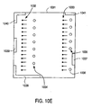
- An interconnect assembly comprising:wherein said stop structure (916, 922, 932, 933, 934, 935) comprises a sheet (903, 931, 953) of material with at least one opening (905, 907, 909, 911, 956, 963).a first substrate (902, 915, 921, 952);a plurality of first contact element (911, 923, 957, 964) disposed on said first substrate (902, 915, 921, 952); anda stop structure (916, 922, 932, 933, 934, 935) disposed on first said substrate,
- The interconnect assembly of claim 1, wherein:said first contact elements (911, 923, 957, 964) are resilient and each has at least a portion thereof which is capable of moving to a first position while a force is applied against said resilient contact element, andsaid stop structure (916, 922, 932, 933, 934, 935) defines said first position.
- The interconnect assembly as in claim 2, further comprising a plurality of second contact elements disposed on a second substrate, and wherein said stop structure (916, 922, 932, 933, 934, 935) defines a separation between said first substrate and said second substrate when said first resilient contact elements (911, 923, 957, 964) are in mechanical and electrical contact with said second contact element.
- The interconnect assembly as in claim 3 wherein said first resilient contact elements comprise spring structures.
- The interconnect assembly as in claim 3 wherein said first substrate and said second substrate are forced toward each other by a vacuum generated between said first substrate and said second substrate.
- The interconnect assembly as in claim 3 wherein said first substrate and said second substrate are forced toward each other by one of a pressurized bladder (1255) or a bellows (1105) and wherein a fluid in said bladder or said bellows is capable of controlling a temperature of at least one of said first substrate and said second substrate.
- The interconnect assembly as in claim 3 wherein said interconnect assembly is part of a probe card assembly (500).
- The interconnect assembly as in claim 3 wherein said interconnect assembly is part of a wafer-level test assembly.
- The interconnect assembly as in claim 3 wherein said stop structure is formed lithographically.
- The interconnect assembly as in claim 3 wherein said stop structure is formed from one of (a) a photoresist material; (b) an epoxy material; (c) a metal coated with an electrophoretic epoxy or (d) a polymeric material.
- The interconnect assembly as in claim 2, further comprising a plurality of openings, and wherein each said first resilient contact elements is disposed in corresponding one of said openings.
- The interconnect assembly as in claim 2 wherein said sheet material comprises an adhesive layer.
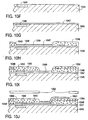
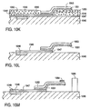
- A method for providing a stop structure for contact elements on a first substrate (902; 952; 623), said method comprising:forming a plurality of openings (905, 907; 956, 963) in a sheet (903; 953);applying said sheet (903; 953) to a first substrate (902; 952; 623); andforming a plurality of contact members (911; 957, 964; 624, 625) on said first substrate (902; 952; 623) in locations corresponding to said plurality of openings (905, 907; 956, 963), wherein at least one region of said sheet (903; 953) disposed around at least one of said openings is said stop structure.
- A method for providing a stop structure for contact elements on a first substrate (902; 952; 623), said method comprising:applying a sheet (903; 953) to a first substrate (902; 952; 623);forming a plurality of openings (905, 907; 956, 963) in said sheet (903; 953); andforming a plurality of contact members (911; 957, 964; 624, 625) on said first substrate (902; 952; 623) in locations corresponding to said plurality of openings (905, 907; 956, 963), wherein at least one region of said sheet (903; 953) disposed around at least one of said openings is said stop structure.
- The method as in claim 13 or 14 wherein said stop structure defines a first position of a first resilient contact element (629) on a second substrate (622) in which said first resilient contact element (629) is in mechanical and electrical contact with one of said contact members (624, 625) in said at least one of said openings (956, 963).
- The method as in claim 13 or 14 wherein each of said contact members comprises a first resilient contact element (905, 907; 957, 964) disposed on said first substrate (902; 952) and which is capable of moving to a first position and wherein said stop structure defines said first position in which said first resilient contact element (911; 952) is in mechanical and electrical contact with a second contact element (605) on a second substrate (603).
- The method as in claim 13 or 14 wherein said first substrate (902; 952; 623) is a wafer of semiconductor integrated circuits and said sheet (903; 953) fits on said wafer.
- The method as in claim 13 or 14 wherein said sheet (903; 953) comprises a polyimide material.
- The method as in claim 13 or 14 further comprising applying an adhesive layer to said sheet (903; 953).
- The method as in claim 13 wherein said plurality of openings (956, 963) is formed before applying said sheet (903; 953) to said first substrate (902; 952; 623) and wherein said plurality of contact members (911; 957, 964; 624, 625) are formed before said sheet is applied to said first substrate.
Priority Applications (1)
| Application Number | Priority Date | Filing Date | Title |
|---|---|---|---|
| EP05012415A EP1583406A3 (en) | 1998-07-13 | 1999-01-04 | Interconnect assembly for printed circuit boards |
Applications Claiming Priority (3)
| Application Number | Priority Date | Filing Date | Title |
|---|---|---|---|
| US114586 | 1998-07-13 | ||
| US09/114,586 US6705876B2 (en) | 1998-07-13 | 1998-07-13 | Electrical interconnect assemblies and methods |
| PCT/US1999/000322 WO2000003569A1 (en) | 1998-07-13 | 1999-01-04 | Interconnect assembly for printed circuit boards and method of fabrication |
Related Child Applications (1)
| Application Number | Title | Priority Date | Filing Date |
|---|---|---|---|
| EP05012415A Division EP1583406A3 (en) | 1998-07-13 | 1999-01-04 | Interconnect assembly for printed circuit boards |
Publications (2)
| Publication Number | Publication Date |
|---|---|
| EP1097617A1 EP1097617A1 (en) | 2001-05-09 |
| EP1097617B1 true EP1097617B1 (en) | 2005-07-20 |
Family
ID=22356165
Family Applications (2)
| Application Number | Title | Priority Date | Filing Date |
|---|---|---|---|
| EP99901354A Expired - Lifetime EP1097617B1 (en) | 1998-07-13 | 1999-01-04 | Interconnect assembly for printed circuit boards and method of fabrication |
| EP05012415A Withdrawn EP1583406A3 (en) | 1998-07-13 | 1999-01-04 | Interconnect assembly for printed circuit boards |
Family Applications After (1)
| Application Number | Title | Priority Date | Filing Date |
|---|---|---|---|
| EP05012415A Withdrawn EP1583406A3 (en) | 1998-07-13 | 1999-01-04 | Interconnect assembly for printed circuit boards |
Country Status (9)
| Country | Link |
|---|---|
| US (4) | US6705876B2 (en) |
| EP (2) | EP1097617B1 (en) |
| JP (2) | JP3949377B2 (en) |
| KR (1) | KR100423683B1 (en) |
| CN (1) | CN1203739C (en) |
| AU (1) | AU2107299A (en) |
| DE (1) | DE69926241T2 (en) |
| TW (1) | TW404033B (en) |
| WO (1) | WO2000003569A1 (en) |
Families Citing this family (79)
| Publication number | Priority date | Publication date | Assignee | Title |
|---|---|---|---|---|
| US6705876B2 (en) * | 1998-07-13 | 2004-03-16 | Formfactor, Inc. | Electrical interconnect assemblies and methods |
| US7435108B1 (en) * | 1999-07-30 | 2008-10-14 | Formfactor, Inc. | Variable width resilient conductive contact structures |
| US6468098B1 (en) * | 1999-08-17 | 2002-10-22 | Formfactor, Inc. | Electrical contactor especially wafer level contactor using fluid pressure |
| US6827584B2 (en) * | 1999-12-28 | 2004-12-07 | Formfactor, Inc. | Interconnect for microelectronic structures with enhanced spring characteristics |
| US6640432B1 (en) | 2000-04-12 | 2003-11-04 | Formfactor, Inc. | Method of fabricating shaped springs |
| US7458816B1 (en) | 2000-04-12 | 2008-12-02 | Formfactor, Inc. | Shaped spring |
| JP4509437B2 (en) * | 2000-09-11 | 2010-07-21 | Hoya株式会社 | Manufacturing method of multilayer wiring board |
| US7396236B2 (en) * | 2001-03-16 | 2008-07-08 | Formfactor, Inc. | Wafer level interposer |
| US6627980B2 (en) | 2001-04-12 | 2003-09-30 | Formfactor, Inc. | Stacked semiconductor device assembly with microelectronic spring contacts |
| DE10143790B4 (en) * | 2001-09-06 | 2007-08-02 | Infineon Technologies Ag | Electronic component with at least one semiconductor chip |
| US6759311B2 (en) | 2001-10-31 | 2004-07-06 | Formfactor, Inc. | Fan out of interconnect elements attached to semiconductor wafer |
| US7385821B1 (en) | 2001-12-06 | 2008-06-10 | Apple Inc. | Cooling method for ICS |
| US20050184748A1 (en) * | 2003-02-04 | 2005-08-25 | Microfabrica Inc. | Pin-type probes for contacting electronic circuits and methods for making such probes |
| US20060051948A1 (en) * | 2003-02-04 | 2006-03-09 | Microfabrica Inc. | Microprobe tips and methods for making |
| US20060006888A1 (en) * | 2003-02-04 | 2006-01-12 | Microfabrica Inc. | Electrochemically fabricated microprobes |
| US7363705B2 (en) * | 2003-02-04 | 2008-04-29 | Microfabrica, Inc. | Method of making a contact |
| US20050104609A1 (en) * | 2003-02-04 | 2005-05-19 | Microfabrica Inc. | Microprobe tips and methods for making |
| US7640651B2 (en) * | 2003-12-31 | 2010-01-05 | Microfabrica Inc. | Fabrication process for co-fabricating multilayer probe array and a space transformer |
| US7273812B2 (en) * | 2002-05-07 | 2007-09-25 | Microfabrica Inc. | Microprobe tips and methods for making |
| US20060053625A1 (en) * | 2002-05-07 | 2006-03-16 | Microfabrica Inc. | Microprobe tips and methods for making |
| US20060238209A1 (en) * | 2002-05-07 | 2006-10-26 | Microfabrica Inc. | Vertical microprobes for contacting electronic components and method for making such probes |
| US7412767B2 (en) * | 2003-02-04 | 2008-08-19 | Microfabrica, Inc. | Microprobe tips and methods for making |
| US7531077B2 (en) | 2003-02-04 | 2009-05-12 | Microfabrica Inc. | Electrochemical fabrication process for forming multilayer multimaterial microprobe structures |
| US7265565B2 (en) * | 2003-02-04 | 2007-09-04 | Microfabrica Inc. | Cantilever microprobes for contacting electronic components and methods for making such probes |
| US6905914B1 (en) | 2002-11-08 | 2005-06-14 | Amkor Technology, Inc. | Wafer level package and fabrication method |
| US7723210B2 (en) | 2002-11-08 | 2010-05-25 | Amkor Technology, Inc. | Direct-write wafer level chip scale package |
| US7084650B2 (en) * | 2002-12-16 | 2006-08-01 | Formfactor, Inc. | Apparatus and method for limiting over travel in a probe card assembly |
| US8088158B2 (en) * | 2002-12-20 | 2012-01-03 | Boston Scientific Scimed, Inc. | Radiopaque ePTFE medical devices |
| US20080211524A1 (en) * | 2003-02-04 | 2008-09-04 | Microfabrica Inc. | Electrochemically Fabricated Microprobes |
| US20080106280A1 (en) * | 2003-02-04 | 2008-05-08 | Microfabrica Inc. | Vertical Microprobes for Contacting Electronic Components and Method for Making Such Probes |
| US9244101B2 (en) * | 2003-02-04 | 2016-01-26 | University Of Southern California | Electrochemical fabrication process for forming multilayer multimaterial microprobe structures |
| US10416192B2 (en) | 2003-02-04 | 2019-09-17 | Microfabrica Inc. | Cantilever microprobes for contacting electronic components |
| US7567089B2 (en) * | 2003-02-04 | 2009-07-28 | Microfabrica Inc. | Two-part microprobes for contacting electronic components and methods for making such probes |
| US8613846B2 (en) * | 2003-02-04 | 2013-12-24 | Microfabrica Inc. | Multi-layer, multi-material fabrication methods for producing micro-scale and millimeter-scale devices with enhanced electrical and/or mechanical properties |
| TW579104U (en) * | 2003-04-09 | 2004-03-01 | Hon Hai Prec Ind Co Ltd | Electrical connector |
| US9671429B2 (en) | 2003-05-07 | 2017-06-06 | University Of Southern California | Multi-layer, multi-material micro-scale and millimeter-scale devices with enhanced electrical and/or mechanical properties |
| TWM249244U (en) * | 2003-07-18 | 2004-11-01 | Hon Hai Prec Ind Co Ltd | Electrical connector |
| US7345350B2 (en) | 2003-09-23 | 2008-03-18 | Micron Technology, Inc. | Process and integration scheme for fabricating conductive components, through-vias and semiconductor components including conductive through-wafer vias |
| US10641792B2 (en) | 2003-12-31 | 2020-05-05 | University Of Southern California | Multi-layer, multi-material micro-scale and millimeter-scale devices with enhanced electrical and/or mechanical properties |
| US20080108221A1 (en) * | 2003-12-31 | 2008-05-08 | Microfabrica Inc. | Microprobe Tips and Methods for Making |
| JP4592292B2 (en) * | 2004-01-16 | 2010-12-01 | 株式会社日本マイクロニクス | Electrical connection device |
| US7282932B2 (en) * | 2004-03-02 | 2007-10-16 | Micron Technology, Inc. | Compliant contact pin assembly, card system and methods thereof |
| US7128580B2 (en) * | 2004-04-09 | 2006-10-31 | Hon Hai Precision Ind. Co., Ltd. | Socket connector with supporting housing protrusions |
| TWM267656U (en) * | 2004-08-20 | 2005-06-11 | Hon Hai Prec Ind Co Ltd | Land grid array electrical connector |
| US7053644B1 (en) * | 2004-12-15 | 2006-05-30 | Aehr Test Systems | System for testing and burning in of integrated circuits |
| US7442049B2 (en) * | 2005-02-09 | 2008-10-28 | International Business Machines Corporation | Electrical connecting device and method of forming same |
| KR20080002793A (en) * | 2005-03-01 | 2008-01-04 | 에스브이 프로브 피티이 엘티디 | Probe card with stacked substrate |
| JP2006261566A (en) * | 2005-03-18 | 2006-09-28 | Alps Electric Co Ltd | Holder and holding sheet for electronic component, electronic module using them, laminate of electronic module, and manufacturing method and inspecting method for electronic module |
| JP2006261565A (en) * | 2005-03-18 | 2006-09-28 | Alps Electric Co Ltd | Electronic functional component mounted body and its manufacturing method |
| JP4036872B2 (en) * | 2005-05-18 | 2008-01-23 | アルプス電気株式会社 | Manufacturing method of semiconductor device |
| JP2007053071A (en) | 2005-07-20 | 2007-03-01 | Alps Electric Co Ltd | Connection element and circuit connection device using the same |
| US7572681B1 (en) | 2005-12-08 | 2009-08-11 | Amkor Technology, Inc. | Embedded electronic component package |
| US7382143B2 (en) * | 2006-05-18 | 2008-06-03 | Centipede Systems, Inc. | Wafer probe interconnect system |
| US7902660B1 (en) | 2006-05-24 | 2011-03-08 | Amkor Technology, Inc. | Substrate for semiconductor device and manufacturing method thereof |
| US7442045B1 (en) | 2007-08-17 | 2008-10-28 | Centipede Systems, Inc. | Miniature electrical ball and tube socket with self-capturing multiple-contact-point coupling |
| JP2009192309A (en) * | 2008-02-13 | 2009-08-27 | Shinko Electric Ind Co Ltd | Semiconductor inspection device |
| US7936177B2 (en) * | 2008-03-07 | 2011-05-03 | Formfactor, Inc. | Providing an electrically conductive wall structure adjacent a contact structure of an electronic device |
| US20100188825A1 (en) * | 2009-01-28 | 2010-07-29 | Honeywell International Inc. | Apparatus for isolating multiple circuit boards from vibration |
| US8796561B1 (en) | 2009-10-05 | 2014-08-05 | Amkor Technology, Inc. | Fan out build up substrate stackable package and method |
| US8937381B1 (en) | 2009-12-03 | 2015-01-20 | Amkor Technology, Inc. | Thin stackable package and method |
| US9691734B1 (en) | 2009-12-07 | 2017-06-27 | Amkor Technology, Inc. | Method of forming a plurality of electronic component packages |
| US8324511B1 (en) | 2010-04-06 | 2012-12-04 | Amkor Technology, Inc. | Through via nub reveal method and structure |
| US8294276B1 (en) | 2010-05-27 | 2012-10-23 | Amkor Technology, Inc. | Semiconductor device and fabricating method thereof |
| US8440554B1 (en) | 2010-08-02 | 2013-05-14 | Amkor Technology, Inc. | Through via connected backside embedded circuit features structure and method |
| US8487445B1 (en) | 2010-10-05 | 2013-07-16 | Amkor Technology, Inc. | Semiconductor device having through electrodes protruding from dielectric layer |
| US8791501B1 (en) | 2010-12-03 | 2014-07-29 | Amkor Technology, Inc. | Integrated passive device structure and method |
| US8390130B1 (en) | 2011-01-06 | 2013-03-05 | Amkor Technology, Inc. | Through via recessed reveal structure and method |
| DE102011109808B4 (en) | 2011-08-08 | 2022-09-22 | Volkswagen Aktiengesellschaft | Process for producing a component connection by element friction welding |
| US8552548B1 (en) | 2011-11-29 | 2013-10-08 | Amkor Technology, Inc. | Conductive pad on protruding through electrode semiconductor device |
| US9129943B1 (en) | 2012-03-29 | 2015-09-08 | Amkor Technology, Inc. | Embedded component package and fabrication method |
| US9048298B1 (en) | 2012-03-29 | 2015-06-02 | Amkor Technology, Inc. | Backside warpage control structure and fabrication method |
| JP2013080938A (en) * | 2012-11-26 | 2013-05-02 | Japan Electronic Materials Corp | Semiconductor inspection device |
| JP6500258B2 (en) * | 2015-06-12 | 2019-04-17 | 北川工業株式会社 | Contact member |
| US9876307B2 (en) | 2015-09-03 | 2018-01-23 | Apple Inc. | Surface connector with silicone spring member |
| US9899757B2 (en) * | 2015-09-03 | 2018-02-20 | Apple Inc. | Surface connector with silicone spring member |
| US9801269B1 (en) * | 2016-05-10 | 2017-10-24 | Northrop Grumman Systems Corporation | Resilient miniature integrated electrical connector |
| JP6858945B2 (en) * | 2016-06-09 | 2021-04-14 | 日本電産リード株式会社 | Inspection jigs, inspection equipment, and probes |
| DE102017002150A1 (en) * | 2017-03-06 | 2018-09-06 | Rosenberger Hochfrequenztechnik Gmbh & Co. Kg | Electrical contact element |
| US11262383B1 (en) | 2018-09-26 | 2022-03-01 | Microfabrica Inc. | Probes having improved mechanical and/or electrical properties for making contact between electronic circuit elements and methods for making |
Family Cites Families (76)
| Publication number | Priority date | Publication date | Assignee | Title |
|---|---|---|---|---|
| US923327A (en) * | 1908-10-17 | 1909-06-01 | Frank A Champlin | Electrical-connection rosette. |
| US4205588A (en) * | 1958-06-10 | 1980-06-03 | The United States Of America As Represented By The Secretary Of The Navy | Method and material for fuze render safe procedure |
| US3193793A (en) * | 1963-03-14 | 1965-07-06 | Kenneth W Plunkett | Electronic connector |
| US3290636A (en) * | 1963-09-30 | 1966-12-06 | Northern Electric Co | Thin-film circuit connector |
| US3573617A (en) * | 1967-10-27 | 1971-04-06 | Aai Corp | Method and apparatus for testing packaged integrated circuits |
| US3936930A (en) * | 1972-07-10 | 1976-02-10 | Rca Corporation | Method of making electrical connections for liquid crystal cells |
| US3842189A (en) * | 1973-01-08 | 1974-10-15 | Rca Corp | Contact array and method of making the same |
| US3794953A (en) * | 1973-01-22 | 1974-02-26 | Security Instr Inc | Electrical terminal for conductive foil |
| US4029375A (en) * | 1976-06-14 | 1977-06-14 | Electronic Engineering Company Of California | Miniature electrical connector |
| US4209745A (en) * | 1978-06-12 | 1980-06-24 | Everett/Charles, Inc. | Interchangeable test head for loaded test member |
| US4202588A (en) * | 1978-11-29 | 1980-05-13 | Technical Wire Products | Electrical connector and support means therefor |
| US4239312A (en) * | 1978-11-29 | 1980-12-16 | Hughes Aircraft Company | Parallel interconnect for planar arrays |
| US4352061A (en) * | 1979-05-24 | 1982-09-28 | Fairchild Camera & Instrument Corp. | Universal test fixture employing interchangeable wired personalizers |
| JPS56116282A (en) * | 1980-02-19 | 1981-09-11 | Sharp Kk | Electronic part with plural terminals |
| US4403272A (en) * | 1980-06-02 | 1983-09-06 | Oak Industries Inc. | Membrane switch interconnect tail and printed circuit board connection |
| US4428633A (en) * | 1982-03-01 | 1984-01-31 | Amp Incorporated | Dual-in-line socket assembly |
| JPS5987842A (en) * | 1982-11-10 | 1984-05-21 | Toshiba Corp | Socket for integrated circuit/large scale integrated circuit |
| US4553192A (en) * | 1983-08-25 | 1985-11-12 | International Business Machines Corporation | High density planar interconnected integrated circuit package |
| US4615573A (en) * | 1983-10-28 | 1986-10-07 | Honeywell Inc. | Spring finger interconnect for IC chip carrier |
| US6330164B1 (en) * | 1985-10-18 | 2001-12-11 | Formfactor, Inc. | Interconnect assemblies and methods including ancillary electronic component connected in immediate proximity of semiconductor device |
| US6043563A (en) | 1997-05-06 | 2000-03-28 | Formfactor, Inc. | Electronic components with terminals and spring contact elements extending from areas which are remote from the terminals |
| US5917707A (en) | 1993-11-16 | 1999-06-29 | Formfactor, Inc. | Flexible contact structure with an electrically conductive shell |
| US5476211A (en) | 1993-11-16 | 1995-12-19 | Form Factor, Inc. | Method of manufacturing electrical contacts, using a sacrificial member |
| US5829128A (en) * | 1993-11-16 | 1998-11-03 | Formfactor, Inc. | Method of mounting resilient contact structures to semiconductor devices |
| US4770641A (en) * | 1986-03-31 | 1988-09-13 | Amp Incorporated | Conductive gel interconnection apparatus |
| US4988306A (en) * | 1989-05-16 | 1991-01-29 | Labinal Components And Systems, Inc. | Low-loss electrical interconnects |
| US5264268B1 (en) * | 1986-07-15 | 1998-12-22 | Mcneil Ppc Inc | Sanitary napkin with composite cover |
| US4813129A (en) | 1987-06-19 | 1989-03-21 | Hewlett-Packard Company | Interconnect structure for PC boards and integrated circuits |
| JPS6447090A (en) * | 1987-08-18 | 1989-02-21 | Seiko Epson Corp | Circuit board |
| JPS6447090U (en) | 1987-09-17 | 1989-03-23 | ||
| JPH01313969A (en) * | 1988-06-13 | 1989-12-19 | Hitachi Ltd | Semiconductor device |
| US4871316A (en) * | 1988-10-17 | 1989-10-03 | Microelectronics And Computer Technology Corporation | Printed wire connector |
| US5366380A (en) * | 1989-06-13 | 1994-11-22 | General Datacomm, Inc. | Spring biased tapered contact elements for electrical connectors and integrated circuit packages |
| US5030109A (en) * | 1990-08-24 | 1991-07-09 | Amp Incorporated | Area array connector for substrates |
| US5136238A (en) * | 1990-11-26 | 1992-08-04 | Electro-Fix, Inc. | Test fixture with diaphragm board with one or more internal grounded layers |
| US5172050A (en) | 1991-02-15 | 1992-12-15 | Motorola, Inc. | Micromachined semiconductor probe card |
| FR2680284B1 (en) | 1991-08-09 | 1993-12-03 | Thomson Csf | VERY LOW PIT CONNECTION DEVICE AND MANUFACTURING METHOD. |
| JPH0564784A (en) | 1991-09-04 | 1993-03-19 | Easy Net:Kk | Electrode type water treatment device |
| DE4135887A1 (en) * | 1991-10-31 | 1993-05-06 | Wolfram Dr. 4040 Neuss De Seiler | DEVICE FOR DEFROSTING COLD DRYERS UNDER 0 (DEGREE) C |
| US5199889A (en) * | 1991-11-12 | 1993-04-06 | Jem Tech | Leadless grid array socket |
| US5309324A (en) * | 1991-11-26 | 1994-05-03 | Herandez Jorge M | Device for interconnecting integrated circuit packages to circuit boards |
| US5252916A (en) * | 1992-01-27 | 1993-10-12 | Everett Charles Technologies, Inc. | Pneumatic test fixture with springless test probes |
| US5338208A (en) * | 1992-02-04 | 1994-08-16 | International Business Machines Corporation | High density electronic connector and method of assembly |
| JPH0669663A (en) | 1992-08-18 | 1994-03-11 | Sony Corp | Multilayered substrate incorporating capacitor |
| EP0615131A1 (en) | 1993-03-10 | 1994-09-14 | Co-Operative Facility For Aging Tester Development | Prober for semiconductor integrated circuit element wafer |
| US5373231A (en) | 1993-06-10 | 1994-12-13 | G. G. B. Industries, Inc. | Integrated circuit probing apparatus including a capacitor bypass structure |
| JP3293334B2 (en) * | 1993-08-25 | 2002-06-17 | セイコーエプソン株式会社 | Semiconductor device and manufacturing method thereof |
| JP2963828B2 (en) | 1993-09-24 | 1999-10-18 | 東京エレクトロン株式会社 | Probe device |
| US5573172A (en) * | 1993-11-08 | 1996-11-12 | Sawtek, Inc. | Surface mount stress relief hidden lead package device and method |
| JP3400051B2 (en) * | 1993-11-10 | 2003-04-28 | ザ ウィタカー コーポレーション | Anisotropic conductive film, method of manufacturing the same, and connector using the same |
| US5974662A (en) | 1993-11-16 | 1999-11-02 | Formfactor, Inc. | Method of planarizing tips of probe elements of a probe card assembly |
| US5772451A (en) | 1993-11-16 | 1998-06-30 | Form Factor, Inc. | Sockets for electronic components and methods of connecting to electronic components |
| US6482013B2 (en) | 1993-11-16 | 2002-11-19 | Formfactor, Inc. | Microelectronic spring contact element and electronic component having a plurality of spring contact elements |
| US5475317A (en) * | 1993-12-23 | 1995-12-12 | Epi Technologies, Inc. | Singulated bare die tester and method of performing forced temperature electrical tests and burn-in |
| US5495667A (en) * | 1994-11-07 | 1996-03-05 | Micron Technology, Inc. | Method for forming contact pins for semiconductor dice and interconnects |
| KR100335165B1 (en) | 1994-11-15 | 2002-05-04 | 이고르 와이. 칸드로스 | Mounting spring elements on semiconductor devices |
| KR100324059B1 (en) | 1994-11-15 | 2002-04-17 | 이고르 와이. 칸드로스 | Interconnection Elements for Microelectronic Components |
| US5633535A (en) * | 1995-01-27 | 1997-05-27 | Chao; Clinton C. | Spacing control in electronic device assemblies |
| JP2876106B2 (en) * | 1995-01-31 | 1999-03-31 | タバイエスペック株式会社 | Composite for burn-in and burn-in device using the composite |
| US5773986A (en) * | 1995-04-03 | 1998-06-30 | Motorola, Inc | Semiconductor wafer contact system and method for contacting a semiconductor wafer |
| JP2968051B2 (en) | 1995-05-26 | 1999-10-25 | フォームファクター,インコーポレイテッド | Chip interconnect carrier and method for mounting a spring contact on a semiconductor device |
| EP0886894B1 (en) | 1995-05-26 | 2005-09-28 | Formfactor, Inc. | Contact carriers for populating substrates with spring contacts |
| JP2799973B2 (en) | 1995-07-06 | 1998-09-21 | 日本電子材料株式会社 | Vertically actuated probe card |
| US5869961A (en) * | 1995-07-31 | 1999-02-09 | Spinner; Howard D. | Smart IC-test receptacle having holes adapted for mounting capacitors arranged adjacent to pin positions |
| JPH0945740A (en) | 1995-08-01 | 1997-02-14 | Nippon Steel Corp | Semiconductor substrate evaluating method and check board therefor |
| WO1997043654A1 (en) | 1996-05-17 | 1997-11-20 | Formfactor, Inc. | Microelectronic spring contact elements |
| WO1998001906A1 (en) | 1996-07-05 | 1998-01-15 | Formfactor, Inc. | Floating lateral support for ends of elongate interconnection elements |
| JPH10125857A (en) | 1996-10-18 | 1998-05-15 | Fuji Electric Co Ltd | Board having built-in capacitor and electronic device using the board |
| US5952840A (en) * | 1996-12-31 | 1999-09-14 | Micron Technology, Inc. | Apparatus for testing semiconductor wafers |
| US6072323A (en) * | 1997-03-03 | 2000-06-06 | Micron Technology, Inc. | Temporary package, and method system for testing semiconductor dice having backside electrodes |
| US6224396B1 (en) * | 1997-07-23 | 2001-05-01 | International Business Machines Corporation | Compliant, surface-mountable interposer |
| US6114240A (en) * | 1997-12-18 | 2000-09-05 | Micron Technology, Inc. | Method for fabricating semiconductor components using focused laser beam |
| US6664628B2 (en) * | 1998-07-13 | 2003-12-16 | Formfactor, Inc. | Electronic component overlapping dice of unsingulated semiconductor wafer |
| US6705876B2 (en) * | 1998-07-13 | 2004-03-16 | Formfactor, Inc. | Electrical interconnect assemblies and methods |
| US6694941B2 (en) * | 2001-08-24 | 2004-02-24 | Kioritz Corporation | Starter |
| US7084650B2 (en) * | 2002-12-16 | 2006-08-01 | Formfactor, Inc. | Apparatus and method for limiting over travel in a probe card assembly |
-
1998
- 1998-07-13 US US09/114,586 patent/US6705876B2/en not_active Expired - Fee Related
- 1998-12-18 TW TW087121224A patent/TW404033B/en not_active IP Right Cessation
-
1999
- 1999-01-04 AU AU21072/99A patent/AU2107299A/en not_active Abandoned
- 1999-01-04 JP JP2000559717A patent/JP3949377B2/en not_active Expired - Fee Related
- 1999-01-04 DE DE69926241T patent/DE69926241T2/en not_active Expired - Lifetime
- 1999-01-04 EP EP99901354A patent/EP1097617B1/en not_active Expired - Lifetime
- 1999-01-04 CN CNB998105392A patent/CN1203739C/en not_active Expired - Fee Related
- 1999-01-04 KR KR10-2001-7000547A patent/KR100423683B1/en not_active IP Right Cessation
- 1999-01-04 WO PCT/US1999/000322 patent/WO2000003569A1/en active IP Right Grant
- 1999-01-04 EP EP05012415A patent/EP1583406A3/en not_active Withdrawn
-
2003
- 2003-12-12 US US10/735,226 patent/US6948941B2/en not_active Expired - Fee Related
-
2004
- 2004-03-09 JP JP2004065217A patent/JP4389209B2/en not_active Expired - Fee Related
-
2005
- 2005-09-27 US US11/237,090 patent/US7169646B2/en not_active Expired - Fee Related
-
2007
- 2007-01-30 US US11/669,068 patent/US7618281B2/en not_active Expired - Fee Related
Also Published As
| Publication number | Publication date |
|---|---|
| US20040127074A1 (en) | 2004-07-01 |
| US20010012704A1 (en) | 2001-08-09 |
| US7618281B2 (en) | 2009-11-17 |
| EP1097617A1 (en) | 2001-05-09 |
| US7169646B2 (en) | 2007-01-30 |
| US20070123082A1 (en) | 2007-05-31 |
| AU2107299A (en) | 2000-02-01 |
| JP4389209B2 (en) | 2009-12-24 |
| DE69926241T2 (en) | 2006-04-20 |
| US20060024988A1 (en) | 2006-02-02 |
| JP2004251910A (en) | 2004-09-09 |
| WO2000003569A1 (en) | 2000-01-20 |
| CN1317224A (en) | 2001-10-10 |
| EP1583406A3 (en) | 2009-09-23 |
| US6705876B2 (en) | 2004-03-16 |
| TW404033B (en) | 2000-09-01 |
| US6948941B2 (en) | 2005-09-27 |
| JP3949377B2 (en) | 2007-07-25 |
| KR20010074710A (en) | 2001-08-09 |
| KR100423683B1 (en) | 2004-03-22 |
| JP2002520864A (en) | 2002-07-09 |
| CN1203739C (en) | 2005-05-25 |
| EP1583406A2 (en) | 2005-10-05 |
| DE69926241D1 (en) | 2005-08-25 |
Similar Documents
| Publication | Publication Date | Title |
|---|---|---|
| EP1097617B1 (en) | Interconnect assembly for printed circuit boards and method of fabrication | |
| US7900347B2 (en) | Method of making a compliant interconnect assembly | |
| US6917525B2 (en) | Construction structures and manufacturing processes for probe card assemblies and packages having wafer level springs | |
| US5414298A (en) | Semiconductor chip assemblies and components with pressure contact | |
| KR20010086060A (en) | Probe card for probing wafers with raised contact elements | |
| WO2010025175A1 (en) | Test contact system for testing integrated circuits with packages having an array of signal and power contacts | |
| WO1997044859A1 (en) | Connectors for microelectronic elements | |
| US5629630A (en) | Semiconductor wafer contact system and method for contacting a semiconductor wafer | |
| US5977784A (en) | Method of performing an operation on an integrated circuit | |
| KR100707044B1 (en) | Construction structures and manufacturing processes for integrated circuit wafer probe card assemblies | |
| KR19990021982A (en) | Contact carriers (tiles) for anchoring large substrates with spring contacts | |
| JPH0783076B2 (en) | Semiconductor chip test socket |
Legal Events
| Date | Code | Title | Description |
|---|---|---|---|
| PUAI | Public reference made under article 153(3) epc to a published international application that has entered the european phase |
Free format text: ORIGINAL CODE: 0009012 |
|
| 17P | Request for examination filed |
Effective date: 20010209 |
|
| AK | Designated contracting states |
Kind code of ref document: A1 Designated state(s): DE FR GB IT |
|
| RAP1 | Party data changed (applicant data changed or rights of an application transferred) |
Owner name: FORMFACTOR, INC. |
|
| 17Q | First examination report despatched |
Effective date: 20031016 |
|
| GRAP | Despatch of communication of intention to grant a patent |
Free format text: ORIGINAL CODE: EPIDOSNIGR1 |
|
| GRAS | Grant fee paid |
Free format text: ORIGINAL CODE: EPIDOSNIGR3 |
|
| GRAA | (expected) grant |
Free format text: ORIGINAL CODE: 0009210 |
|
| AK | Designated contracting states |
Kind code of ref document: B1 Designated state(s): DE FR GB IT |
|
| PG25 | Lapsed in a contracting state [announced via postgrant information from national office to epo] |
Ref country code: IT Free format text: LAPSE BECAUSE OF FAILURE TO SUBMIT A TRANSLATION OF THE DESCRIPTION OR TO PAY THE FEE WITHIN THE PRESCRIBED TIME-LIMIT;WARNING: LAPSES OF ITALIAN PATENTS WITH EFFECTIVE DATE BEFORE 2007 MAY HAVE OCCURRED AT ANY TIME BEFORE 2007. THE CORRECT EFFECTIVE DATE MAY BE DIFFERENT FROM THE ONE RECORDED. Effective date: 20050720 |
|
| REG | Reference to a national code |
Ref country code: GB Ref legal event code: FG4D |
|
| REF | Corresponds to: |
Ref document number: 69926241 Country of ref document: DE Date of ref document: 20050825 Kind code of ref document: P |
|
| RAP2 | Party data changed (patent owner data changed or rights of a patent transferred) |
Owner name: FORMFACTOR, INC. |
|
| PG25 | Lapsed in a contracting state [announced via postgrant information from national office to epo] |
Ref country code: GB Free format text: LAPSE BECAUSE OF NON-PAYMENT OF DUE FEES Effective date: 20060104 |
|
| ET | Fr: translation filed | ||
| PLBE | No opposition filed within time limit |
Free format text: ORIGINAL CODE: 0009261 |
|
| STAA | Information on the status of an ep patent application or granted ep patent |
Free format text: STATUS: NO OPPOSITION FILED WITHIN TIME LIMIT |
|
| 26N | No opposition filed |
Effective date: 20060421 |
|
| GBPC | Gb: european patent ceased through non-payment of renewal fee |
Effective date: 20060104 |
|
| PG25 | Lapsed in a contracting state [announced via postgrant information from national office to epo] |
Ref country code: FR Free format text: LAPSE BECAUSE OF NON-PAYMENT OF DUE FEES Effective date: 20060131 |
|
| PGFP | Annual fee paid to national office [announced via postgrant information from national office to epo] |
Ref country code: DE Payment date: 20110127 Year of fee payment: 13 |
|
| REG | Reference to a national code |
Ref country code: FR Ref legal event code: ST Effective date: 20110923 |
|
| PG25 | Lapsed in a contracting state [announced via postgrant information from national office to epo] |
Ref country code: DE Free format text: LAPSE BECAUSE OF NON-PAYMENT OF DUE FEES Effective date: 20120801 |
|
| REG | Reference to a national code |
Ref country code: DE Ref legal event code: R119 Ref document number: 69926241 Country of ref document: DE Effective date: 20120801 |