TECHNICAL FIELD OF THE INVENTION
-
This invention relates generally to the field of electronic
devices and, more particularly, to a via capacitor.
BACKGROUND OF THE INVENTION
-
Capacitors are typical elements in integrated circuits.
Decreasing the size of integrated circuits often leads to a
corresponding decrease in the size of the capacitors used in
those circuits. As the size of the capacitors decreases,
difficulty may be encountered in maintaining a high capacitance,
which often leads manufacturers to fabricate capacitors with
higher densities in order to maintain a high capacitance.
However, conventional high density capacitors typically require
additional steps to fabricate, resulting in higher manufacturing
costs.
-
In an effort to maintain capacitance levels without
increasing fabrication costs, manufacturers of integrated
circuits may use larger capacitors rather than smaller, high
density capacitors. A disadvantage associated with this method
is that the larger capacitors occupy physical space that could
be used for other physical elements of the integrated circuits.
SUMMARY OF THE INVENTION
-
The present invention recognizes a need for an improved via
capacitor and a method for manufacturing a via capacitor that
reduces or eliminates many shortcomings of prior systems and
methods.
-
In accordance with one aspect of the present invention, a
capacitor comprises a first conductive layer disposed outwardly
from a semiconductor substrate and comprising a first plate and
a second plate. The capacitor also comprises a first via layer
disposed outwardly from the first conductive layer and
comprising a first via coupled to the first plate and a second
via coupled to the second plate. The first and second vias are
separated by a dielectric and are each operable to be charged
with different potentials to establish a capacitance between the
first and second vias. The capacitor further comprises a second
conductive layer disposed outwardly from the first via layer and
comprising a third plate coupled to the first via and a fourth
plate coupled to the second via.
-
Technical advantages of the present invention include the
provision of a capacitive structure that uses inter-layer vias
to contribute to the overall capacitance of the structure.
While vias have been typically used to connect elements in an
integrated circuit to a power supply, vias are not typically
used in conventional capacitors and have never been used to
actually contribute to the capacitance of the device.
Conventional capacitors typically include two oppositely
polarized conductive layers disposed one on top of the other and
separated by a dielectric. Due to the typically opposite
polarization of the two conductive layers, vias have not been
used to connect the conductive layers because using a via to
connect the layers would create a short circuit. One aspect of
the present invention is the use of vias to couple stacked
conductive layers and to provide a capacitance not only between
adjacent plates in the conductive layers, but also between
adjacent vias. This may be provided using a unique charging
scheme.
-
The invention provides a higher density than other typical
capacitors without the additional costs typically associated
with fabricating high density capacitors. The invention,
therefore, may reduce the costs of integrated circuits. In
addition, multiple alternating layers of vias and conductive
plates can be disposed one on top of the other, resulting in a
stacked via capacitor and further increasing the density of the
capacitor.
-
A further advantage of the via capacitor is the ability to
fabricate the capacitors without adding additional steps to the
fabrication process. The elimination of additional fabrication
steps offers another cost reduction to manufacturers of
integrated circuits.
-
In addition, the via capacitor can be designed to result in
a structure more rigid than other typical capacitors. As
mechanical stresses are applied to an integrated circuit,
typical capacitors may become deformed, reducing the
effectiveness of the capacitor. The via capacitor can be
structured to resist mechanical stresses to a greater degree,
increasing the performance of the capacitor.
-
Other technical advantages are readily apparent to one of
skill in the art from the attached figures, description and
claims.
BRIEF DESCRIPTION OF THE DRAWINGS
-
For a more complete understanding of the present invention
and the advantages thereof, reference is now made to the
following descriptions taken in connection with the accompanying
drawings, in which:
- FIGURE 1 is a cross-sectional view of one exemplary
embodiment of a via capacitor constructed in accordance with the
teachings of the present invention;
- FIGURE 2 is a cross-sectional view of another exemplary
embodiment of a via capacitor constructed in accordance with the
teachings of the present invention;
- FIGURES 3a-3c are cut-away views of the via capacitor shown
in FIGURE 2 along lines 3A-3C, respectively;
- FIGURES 4a-4d illustrate an exemplary series of steps in
the formation of a first conductive layer in a via capacitor;
- FIGURES 5a-5d illustrate an exemplary series of steps in
the formation of a via layer in a via capacitor; and
- FIGURES 6a-6d illustrate an exemplary series of steps in
the formation of a second conductive layer in a via capacitor.
-
DETAILED DESCRIPTION OF THE INVENTION
-
FIGURE 1 is a cross-sectional view of one exemplary
embodiment of a via capacitor 16 constructed in accordance with
the teachings of the present invention. In the illustrated
embodiment, via capacitor 16 resides within an integrated
circuit 10. In this example, integrated circuit 10 comprises a
semiconductor substrate 12, intermediate layer 14 disposed
outwardly from semiconductor substrate 12, and capacitor 16
disposed outwardly from intermediate layer 14. Intermediate
layer 14 may comprise any layer, structure, or combination of
layers and/or structures of integrated circuit 10 disposed
inwardly from capacitor 16. In another embodiment, capacitor 16
may be in direct contact with semiconductor substrate 12 without
any intermediate layers and/or structures 14 separating
semiconductor substrate 12 and capacitor 16.
-
In the illustrated embodiment, capacitor 16 comprises
alternating conductive layers and via layers. A first
conductive layer 18 is disposed outwardly from semiconductor
substrate 12, and a first via layer 20 is disposed outwardly
from first conductive layer 18. A second conductive layer 22 is
disposed outwardly from first via layer 20 and is coupled to
first conductive layer 18 by first via layer 20. In this
document, the term "couple" refers to any direct or indirect
electrical connection between two or more elements. The
elements said to be "coupled" to one another may or may not
physically contact one another.
-
First conductive layer 18 is disposed outwardly from
semiconductor substrate 12. In the illustrated embodiment,
first conductive layer 18 comprises two or more conductive
plates, each separated by a dielectric 32. In this document,
the term "plate" may refer to any uniform or nonuniform
structure capable of forming a lateral capacitance with an
approximately adjacent structure. In this example, first
conductive layer 18 is a feed layer, the plates of first
conductive layer 18 comprising a first feed contact 34a and a
second feed contact 34b disposed approximately adjacent to first
feed contact 34a. Feed contacts 34a and 34b are separated by
dielectric 32. Feed contacts 34 are coupled to a power supply
(not explicitly shown), which allows feed contact 34a to be
charged with one potential and feed contact 34b with a different
potential. In one embodiment, feed contact 34a is operable to
be charged with one potential, and feed contact 34b is operable
to be charged with an approximately equal potential of opposite
polarity.
-
Feed contacts 34 may be formed from any conductive material
or combination of conductive materials including, for example,
copper, aluminum, tungsten, and/or doped polysilicon.
Dielectric 32 may comprise, for example, silicon dioxide,
silicon nitride, silicon carbide, or any other suitable
dielectric material or combination of dielectric materials.
Dielectric 32 may comprise one or multiple layers without
departing from the scope of the invention.
-
Although the illustrated embodiment shows first conductive
layer 18 as the feed layer, the invention is not so limited.
Any conductive layer could be coupled to the power supply and
serve as a feed layer without departing from the scope of the
invention. In addition, although the illustrated embodiment
shows a single feed layer operable to couple both potentials to
capacitor 16, integrated circuit 10 may include multiple feed
layers, each coupling selected nodes 30 of capacitor 16 to a
particular potential power supply.
-
First via layer 20 is disposed outwardly from first
conductive layer 18. In the illustrated embodiment, first via
layer 20 comprises two or more vias coupling first conductive
layer 18 and second conductive layer 22. In this example, first
via layer 20 comprises a first via 36a and a second via 36b.
Vias 36 are separated by dielectric 32. Via 36a is coupled to
feed contact 34a, and via 36b is coupled to feed contact 34b.
Vias 36 may be formed from any conductive material or
combination of conductive materials including, for example,
copper, aluminum, tungsten, and/or doped polysilicon.
Identification of vias in this document as a "first via," a
"second via," a "third via," etc., is for identification
purposes only and is not intended to limit the number of vias in
any particular via layer or in capacitor 16.
-
Second conductive layer 22 is disposed outwardly from first
via layer 20. In the illustrated embodiment, second conductive
layer 22 comprises two or more conductive plates, each separated
by dielectric 32. In this example, second conductive layer 22
comprises a first plate 38a and a second plate 38b disposed
approximately adjacent to first plate 38a. Plates 38 are
coupled to feed contacts 34 by via layer 20. Plate 38a is
coupled to feed contact 34a by via 36a, and plate 38b is coupled
to feed contact 34b by via 36b. Plates 38 may be formed from
any conductive material or combination of conductive materials
including, for example, copper, aluminum, tungsten, and/or doped
polysilicon. Identification of plates in this document as a
"first plate," a "second plate," a "third plate," etc., is for
identification purposes only and is not intended to limit the
number of plates in any particular conductive layer or in
capacitor 16.
-
In the illustrated embodiment, capacitor 16 has two nodes
30a and 30b. Nodes 30a and 30b are separated by dielectric 32.
In one aspect of operation, nodes 30a and 30b are operable to be
charged with differing potentials, creating a capacitance
between feed contacts 34, vias 36, and plates 38 of nodes 30a
and 30b. In a particular embodiment, nodes 30a and 30b are
operable to be charged with approximately equal magnitude,
oppositely polarized charges.
-
Via 36a couples feed contact 34a and plate 38a, and via 36a
and plate 38a are operable to be charged with approximately the
same potential as feed contact 34a. Via 36b couples feed
contact 34b and plate 38b, and via 36b and plate 38b are
operable to be charged with approximately the same potential as
feed contact 34b. Feed contact 34a has a different potential
than feed contact 34b. The difference in potential, appropriate
selection of dielectric 32 between nodes 30, and arrangement of
nodes 30 create a lateral capacitance between feed contacts 34a
and 34b in first conductive layer 18 and between plates 38a and
38b in second conductive layer 22. In addition, the arrangement
and charging of vias 36 along with the presence of dielectric 32
creates an inter-via capacitance between vias 36a and 36b in
first via layer 20. The inter-via capacitance advantageously
contributes to the overall capacitance of capacitor 16.
-
Although the illustrated embodiment of capacitor 16 has
only two nodes 30a and 30b, capacitor 16 may comprise any number
of nodes 30, and each node 30 may comprise any number of
conductive and via layers. In addition, although the
illustrated embodiment shows a single via coupling each plate 34
to a plate 38, any number of vias could be used.
-
Capacitor 16 advantageously provides a high capacitance per
unit of area. The use of vias 36 between conductive layers 18
and 22 creates an inter-via capacitance between vias 36 in via
layer 20, in addition to the capacitance between plates 34 and
38 in conductive layers 18 and 22. The inter-via capacitance
contributes to and increases the overall capacitance of
capacitor 16. Also, capacitor 16 may be fabricated without
additional steps to the fabrication process, reducing the costs
of manufacturing capacitor 16. In addition, capacitor 16 has a
structure that is more rigid than the structures of other
typical capacitors. In the illustrated embodiment, vias 36 in
via layer 20 provide support for plates 34 and 38 in conductive
layers 18 and 22. This support may reduce the amount of
deformation of plates 34 and 38 and allow capacitor 16 to resist
mechanical stresses to a greater degree.
-
FIGURE 2 is a cross-sectional view of another exemplary
embodiment of a via capacitor 116 constructed in accordance with
the teachings of the present invention. Capacitor 116 comprises
a first conductive layer 118, a first via layer 120, a second
conductive layer 122, a second via layer 124, and a third
conductive layer 126.
-
First conductive layer 118 is disposed outwardly from a
semiconductor substrate 112 and comprises a first feed contact
134a and a second feed contact 134b. First conductive layer 118
may be disposed on one or multiple intermediate layers and/or
structures 114 or directly on semiconductor substrate 112.
First via layer 120 is disposed outwardly from first conductive
layer 118 and comprises vias 136a and 136b, and second
conductive layer 122 is disposed outwardly from first via layer
120 and comprises plates 138a and 138b. First conductive layer
118, first via layer 120, and second conductive layer 122 may be
the same as or similar to first conductive layer 18, first via
layer 20, and second conductive layer 22, respectively, from
FIGURE 1.
-
In the illustrated embodiment, second via layer 124 is
disposed outwardly from second conductive layer 122 and
comprises two or more vias. In this embodiment, third
conductive layer 126 is disposed outwardly from second via layer
124 and comprises two or more conductive plates. In this
example, second via layer 124 comprises two vias 140a and 140b,
and third conductive layer 126 comprises two plates 142a and
142b. A dielectric 132 separates each plate 142 from one
another and each via 140 from one another.
-
Via 140a couples plates 138a and 142a, and via 140b couples
plates 138b and 142b. Via 140a and plate 142a are operable to
be charged with approximately the same potential as feed contact
134a, and via 140b and plate 142b are operable to be charged
with approximately the same potential as feed contact 134b. The
structural arrangement of the conductive plates, vias, and
dielectric, as well as the difference in potential, creates a
capacitance between plates 142a and 142b and an inter-via
capacitance between vias 140a and 140b.
-
Plates 142 and vias 140 may be formed from any conductive
material or combination of conductive materials including, for
example, copper, aluminum, tungsten, and/or doped polysilicon.
Dielectric 132 may comprise, for example, silicon dioxide,
silicon nitride, silicon carbide, or any other suitable
dielectric material or materials comprising one or multiple
layers.
-
Capacitor 116 may further comprise any number of
alternating via and conductive layers. Each plate in each
conductive layer in capacitor 116 is coupled to a plate in
another conductive layer by at least one via. The vias are
arranged and charged so that each via having one potential is
approximately adjacent to at least one other via having a
different potential, creating an inter-via capacitance between
the vias in each via layer.
-
Although the illustrated embodiment shows feed contacts 134
in first conductive layer 118, those skilled in the art will
recognize that feed contacts 134a and 134b may be fabricated
anywhere in capacitor 116. Feed contacts 134a and 134b may be
located in third conductive layer 126 or in any other conductive
layer. Feed contacts 134a and 134b could also be located on
different conductive layers within capacitor 116. For example,
feed contact 134a may be fabricated on first conductive layer
118, and feed contact 134b may be fabricated on third conductive
layer 126. In addition, multiple feed contacts may feed each
node 130.
-
FIGURES 3a-3c are cut-away views of via capacitor 116 shown
in FIGURE 2 along lines 3A-3C, respectively. FIGURE 3a is a
cut-away view of capacitor 116 along line 3A illustrated in
FIGURE 2, showing first conductive layer 118 and first via layer
120. In the illustrated embodiment, fist conductive layer 118
is a feed layer comprising first feed contact 134a and second
feed contact 134b. In this embodiment, first feed contact 134a
comprises a plurality of first feed fingers 150, and second feed
contact 134b comprises a plurality of second feed fingers 152.
First feed fingers 150 and second feed fingers 152 are separated
by dielectric 132. In this example, first feed fingers 150 and
second feed fingers 152 are interlaced such that each first feed
finger 150 is approximately adjacent to at least one second feed
finger 152.
-
In the illustrated embodiment, first via layer 120
comprises a plurality of vias 136a coupled to feed contact 134a
and a plurality of vias 136b coupled to feed contact 134b. Vias
136 are separated by dielectric 132. Vias 136a are operable to
be charged with approximately the same potential as feed contact
134a, and vias 136b are operable to be charged with
approximately the same potential as feed contact 134b. Vias 136
are arranged and charged so that each via 136a is approximately
adjacent to at least one via 136b. The difference in potential
and dielectric 132 between vias 136a and 136b creates a
capacitance between vias 136a and 136b.
-
FIGURE 3b is a cut-away view of capacitor 116 along line 3B
illustrated in FIGURE 2, showing second conductive layer 122 and
second via layer 124. In the illustrated embodiment, second
conductive layer 122 comprises a plurality of plates 138a
coupled to feed contact 134a and a plurality of plates 138b
coupled to feed contact 134b. Dielectric 132 separates plates
138 from one another. Each plate 138 is coupled to first
conductive layer 118 by the vias 136 illustrated in FIGURE 3a.
Vias 136a couple plates 138a to feed contact 134a, and plates
138a are operable to be charged with approximately the same
potential as feed contact 134a. Vias 136b couple plates 138b to
feed contact 134b, and plates 138b are operable to be charged
with approximately the same potential as feed contact 134b. The
difference in potential and presence of dielectric 132 creates a
capacitance between plates 138a and 138b.
-
In the illustrated embodiment, second via layer 124
comprises a plurality of vias 140a coupling plates 138a to third
conductive layer 126 and a plurality of vias 140b coupling
plates 138b to third conductive layer 126. Vias 140 are
separated by dielectric 132. Vias 140a are operable to be
charged with approximately the same potential as plates 138a,
which have approximately the same potential as feed contact
134a. Vias 140b are operable to be charged with approximately
the same potential as plates 138b, which have approximately the
same potential as feed contact 134b. Vias 140 are arranged and
charged so that each via 140a is approximately adjacent to at
least one via 140b, and the difference in potential and presence
of dielectric 132 creates a capacitance between vias 140a and
140b.
-
FIGURE 3c is a cut-away view of capacitor 116 along line 3C
illustrated in FIGURE 2, showing third conductive layer 126. In
the illustrated embodiment, third conductive layer 126 comprises
a plurality of plates 142a coupled to plates 138a and a
plurality of plates 142b coupled to plates 138b. Dielectric 132
separates plates 142 from one another. Each plate 142 is
coupled to second conductive layer 122 by the vias 140
illustrated in FIGURE 3b. Vias 140a couple plates 142a to
plates 138a, and plates 142a are operable to be charged with
approximately the same potential as feed contact 134a. Vias
140b couple plates 142b to plates 138b, and plates 142b are
operable to be charged with approximately the same potential as
feed contact 134b. The difference in potential and presence of
dielectric 132 creates a capacitance between plates 142a and
142b.
-
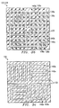
FIGURES 4a-4d illustrate an exemplary series of steps in
the formation of a first conductive layer 18 of a via capacitor
such as via capacitor 16 shown in FIGURE 1. In FIGURE 4a, a
dielectric material 160 is formed outwardly from semiconductor
substrate 12. Dielectric material 160 may be formed directly on
semiconductor substrate 12 or on one or more intermediate layers
and/or structures 14. Dielectric material 160 may comprise any
suitable dielectric material or materials comprising one or
multiple layers. In FIGURE 4b, cavities 162a and 162b are
formed in dielectric material 160 using any appropriate
fabrication process, such as a pattern and etch. Cavities 162
may be formed to approximately conform to the shape of feed
contacts 34. In FIGURE 4c, a conductive material 164 is formed
outwardly from and in cavities 162. Conductive material 164 may
comprise any conductive material or combination of conductive
materials. In FIGURE 4d, dielectric material 160 and conductive
material 164 are polished to form feed contacts 34a and 34b
separated by dielectric 160.
-
Although the illustrated steps show dielectric material 160
being formed before conductive material 164, the invention is
not so limited. The series of steps illustrated in FIGURES 4a-4d
show one particular example of a method of forming feed
contacts 34a and 34b in first conductive layer 18. These
structures could alternatively be formed using a wide variety of
methods. For example, conductive material 164 could initially
be formed outwardly from semiconductor substrate 12 or
intermediate layer 14 and formed into feed contacts 34 using any
appropriate fabrication process, such as a pattern and etch.
Dielectric material 160 can then be formed outwardly from and
between feed contacts 34a and 34b.
-
In addition, although the illustrated embodiment shows the
formation of feed contacts 34a and 34b in first conductive layer
18, similar steps could be used to form plates 38 in first
conductive layer 18.
-
FIGURES 5a-5d illustrate an exemplary series of steps in
the formation of a via layer of a via capacitor such as via
capacitor 16 shown in FIGURE 1. In FIGURE 5a, a dielectric
material 180 is formed outwardly from first conductive layer 18.
Dielectric material 180 may comprise any suitable dielectric
material or materials comprising one or multiple layers, and
dielectric material 180 may be the same as or different than
dielectric material 160. In FIGURE 5b, cavities 182a and 182b
are formed in dielectric material 180 using any appropriate
fabrication process, such as a pattern and etch. Cavities 182
may be formed to approximately conform to the shape of vias 36.
In FIGURE 5c, a conductive material 184 is formed outwardly from
and in cavities 182. Conductive material 184 may comprise any
conductive material or combination of conductive materials, and
conductive material 184 need not be the same as conductive
material 164. In FIGURE 5d, dielectric material 180 and
conductive material 184 are polished to form vias 36a and 36b
separated by dielectric 180.
-
Although the illustrated steps show dielectric material 180
being formed before conductive material 184, the invention is
not so limited. The series of steps illustrated in FIGURES 5a-5d
show one particular method of forming vias 36a and 36b.
These structures could alternately be formed using a wide
variety of methods. For example, conductive material 184 could
initially be formed outwardly from first conductive layer 18
and, using any appropriate fabrication process, formed into vias
36a and 36b. Dielectric material 180 can then be formed
outwardly from and between vias 36a and 36b.
-
In addition, although FIGURES 4a-4d and FIGURES 5a-5d
illustrate the formation of first conductive layer 18 and first
via layer 20 as two independent series of steps, first
conductive layer 18 and first via layer 20 could be formed using
an integrated series of steps. For example, conductive material
164 could be formed outwardly from semiconductor substrate 12
and formed into feed contacts 34. Dielectric material 160 can
be formed between feed contacts 34 in first conductive layer 18
and outwardly in first via layer 20. Cavities 182 could then be
formed in dielectric material 160, and conductive material 184
could be formed outwardly from and in cavities 182. Conductive
material 184 and dielectric material 160 could be polished to
form vias 36 coupled to feed contacts 34.
-
FIGURES 6a-6d illustrate an exemplary series of steps in
the formation of a second conductive layer 22 of a via capacitor
such as via capacitor 16 shown in FIGURE 1. In FIGURE 6a, a
dielectric material 200 is formed outwardly from first via layer
20. Dielectric material 200 may comprise any suitable
dielectric material or materials comprising one or multiple
layers, and dielectric material 200 need not be the same as
dielectric material 160 or 180. In FIGURE 6b, cavities 202a and
202b are formed in dielectric material 200 using any appropriate
fabrication process, such as a pattern and etch. Cavities 202
may be formed to approximately conform to the shape of plates
38. In FIGURE 6c, a conductive material 204 is formed outwardly
from and in cavities 202. Conductive material 204 may comprise
any conductive material or combination of conductive materials,
and conductive material 204 may be the same as or different than
conductive material 164 or 184. In FIGURE 6d, dielectric
material 200 and conductive material 204 are polished to form
plates 38a and 38b separated by dielectric 200.
-
Although the illustrated steps show dielectric material 200
being formed before conductive material 204, other methods,
including the method described above for first conductive layer
18, may be used. Also, although FIGURES 5a-5d and FIGURES 6a-6d
illustrate the formation of first via layer 20 and second
conductive layer 22 as two independent series of steps, first
via layer 20 and second conductive layer 22 could be formed
using an integrated series of steps. For example, conductive
material 164 can be formed outwardly from semiconductor
substrate 12 and formed into feed contacts 34. Dielectric
material 160 can be formed between feed contacts 34 in first
conductive layer 18 and outwardly in first via layer 20 and
second conductive layer 22. Cavities 202 can be formed in
dielectric material 160, and then cavities 182 can be formed in
dielectric material 160. Conductive material 204 can be formed
outwardly from and in cavities 182 and 202. Conductive material
204 and dielectric material 164 can be polished to form vias 36
and plates 38.
-
In addition, although FIGURES 6a-6d have been described as
forming plates 38 in second conductive layer 22, similar steps
could be implemented to form feed contacts 34 in second
conductive layer 22.
-
Although the present invention has been described in
several embodiments, a myriad of changes, variations,
alterations, transformations, and modifications may be suggested
to one skilled in the art, and it is intended that the present
invention encompass such changes, variations, alterations,
transformations, and modifications.