EP1115511B1 - Offset rotor flat media processor - Google Patents
Offset rotor flat media processor Download PDFInfo
- Publication number
- EP1115511B1 EP1115511B1 EP99930500A EP99930500A EP1115511B1 EP 1115511 B1 EP1115511 B1 EP 1115511B1 EP 99930500 A EP99930500 A EP 99930500A EP 99930500 A EP99930500 A EP 99930500A EP 1115511 B1 EP1115511 B1 EP 1115511B1
- Authority
- EP
- European Patent Office
- Prior art keywords
- bowl
- rotor
- processor
- flat media
- openings
- Prior art date
- Legal status (The legal status is an assumption and is not a legal conclusion. Google has not performed a legal analysis and makes no representation as to the accuracy of the status listed.)
- Expired - Lifetime
Links
Images

Classifications
-
- H—ELECTRICITY
- H01—ELECTRIC ELEMENTS
- H01L—SEMICONDUCTOR DEVICES NOT COVERED BY CLASS H10
- H01L21/00—Processes or apparatus adapted for the manufacture or treatment of semiconductor or solid state devices or of parts thereof
- H01L21/67—Apparatus specially adapted for handling semiconductor or electric solid state devices during manufacture or treatment thereof; Apparatus specially adapted for handling wafers during manufacture or treatment of semiconductor or electric solid state devices or components ; Apparatus not specifically provided for elsewhere
- H01L21/67005—Apparatus not specifically provided for elsewhere
- H01L21/67011—Apparatus for manufacture or treatment
- H01L21/67017—Apparatus for fluid treatment
- H01L21/67028—Apparatus for fluid treatment for cleaning followed by drying, rinsing, stripping, blasting or the like
- H01L21/67034—Apparatus for fluid treatment for cleaning followed by drying, rinsing, stripping, blasting or the like for drying
-
- B—PERFORMING OPERATIONS; TRANSPORTING
- B08—CLEANING
- B08B—CLEANING IN GENERAL; PREVENTION OF FOULING IN GENERAL
- B08B3/00—Cleaning by methods involving the use or presence of liquid or steam
- B08B3/02—Cleaning by the force of jets or sprays
-
- Y—GENERAL TAGGING OF NEW TECHNOLOGICAL DEVELOPMENTS; GENERAL TAGGING OF CROSS-SECTIONAL TECHNOLOGIES SPANNING OVER SEVERAL SECTIONS OF THE IPC; TECHNICAL SUBJECTS COVERED BY FORMER USPC CROSS-REFERENCE ART COLLECTIONS [XRACs] AND DIGESTS
- Y10—TECHNICAL SUBJECTS COVERED BY FORMER USPC
- Y10S—TECHNICAL SUBJECTS COVERED BY FORMER USPC CROSS-REFERENCE ART COLLECTIONS [XRACs] AND DIGESTS
- Y10S134/00—Cleaning and liquid contact with solids
- Y10S134/902—Semiconductor wafer
Definitions
- the technical field of this invention is centrifugal processing equipment and methods used to process semiconductor wafers, photomasks, optical and glass disks, magnetic disks, flat panels, lenses or similar flat media.
- the production of semiconductor wafers, substrates and photomask plates used in the manufacture of semiconductor wafers has typically utilized processing equipment in which various types of processing fluids are used to treat the wafers.
- processing equipment in which various types of processing fluids are used to treat the wafers.
- One example of a semiconductor processor is a centrifugal rinser-dryer used to rinse acids, caustics, etchants and other processing fluids from wafers, photomask plates, and similar flat media.
- the rinser-dryers are also used to dry the rinsed units using a flow of heated gas, such as nitrogen, which is passed through the processing chamber after rinsing with the desired fluid.
- heated gas such as nitrogen
- the wafers are spun during processing to provide more even distribution of the processing fluids across the wafer surfaces, and to assist in removal of rinsing liquids in preparation for drying.
- semiconductor processors include acid, solvent, and caustic treatment machines which spray or otherwise apply acids, solvents and caustics to the wafers or other flat media. Stripping processors are used to remove photoresist from the wafers. Other specific processing of semiconductors may require other types of chemicals. Many of these processes are performed in centrifugal processing machines to provide for even distribution of fluids over the wafer and to aid in removal of liquids.
- a primary problem in the production of semiconductors is particle contamination. Contaminant particles can affect the photographic processes used to transfer the chip layouts onto the wafers being processed into chips. Contaminants on the photomasks can cause deterioration of the image being transferred onto the wafer.
- the direct processing of the wafers themselves is even more susceptible to contamination because of the numerous processing steps involved and the risk at each stage that contaminating particles can become adhered to the surface of the wafer.
- Particle contamination causes a large number of the chips in a wafer to be defective. Thus it is very important to reduce contamination to increase yields.
- the causes of contaminating particles on wafer surfaces occurs from numerous sources. Each of the processing fluids used is necessarily impure to some small degree.
- the water used in processing is deionized to remove metallic ions and other impurities, but such supplies also contain some impurities.
- Centrifugal processing is advantageous because spinning the wafers or other flat media flings off fluid droplets. This helps to prevent contamination by "spotting" which occurs if fluid droplets on the wafer evaporate. It is also advantageous to have the used rinse water or fluids removed from the processing chamber as quickly as possible, to prevent recontamination.
- Centrifugal processors such as spray solvent and spray acid processors, and spin rinser dryers, typically have a rotor which spins inside of a cylindrical processing chamber or bowl.
- the cylindrical rotor holds a removable cassette or non-removable combs which carry the wafers.
- the bowl typically has a drainage ditch or channel running from the front to the rear, near the bottom of the bowl, to drain fluids out of the bowl.
- the spinning rotor which is centered in the bowl, generates rapid counter-clockwise air movement within the bowl.
- This air movement hinders the clean drying or other processing operation of the centrifugal processor, as it tends to draw spent fluid droplets of e.g., water, solvent, or acid, up and around in the bowl, allowing droplets to be re-deposited on the wafers or other flat media.
- the air movement also tends to draw droplets away from the drainage channel, allowing them to be disadvantageously recycled back up and around the bowl.
- US 0 471 541 A describes a washing-machine having a base formed with lower converging ends, n vertically-adjustable cylinders within the base, and a cover adapted to rest on the converging ends when in its lowered position.
- US 2 895 320 A describes a washing machine including a cabinet and a rotatable tub at an angle in said cabinet and provided with an inclined axis of rotation.
- the machine for cleaning clothes and the like disclosed in US 3 388 410 A includes a rotatable chamber adapted to receive clothes to be cleaned in a cleaning solution and means for rotating the chamber about its central axis at a relatively high speed.
- the closed cycle dry cleaning apparatus disclosed in US 3 410 118 A comprises a housing, an apertured basket rotatably mounted in said housing, and means for selectively rotating said basket.
- US 4 153 551 A describes a centrifuge having a drum to which a wobble or nutating motion is applied to discharge the centrifuged material over the edge of a wall of the perforated basket.
- the wobble or nutation is caused by tilting the axis of this wall relative to the axis rotation of the assembly.
- the present invention is directed to a centrifugal semiconductor wafer spray processor with a rotor contained within a bowl which is designed to better direct and scavenge fluids from the bowl. By doing so, a more complete process can be accomplished with less risk of contamination from spent fluid.
- the present invention provides a centrifugal semiconductor wafer spray processor as featured in independent claim. Preferred embodiments are described in the dependent claims.
- the centrifugal processor includes a rotor offset from the centerline of the bowl.
- the offset provides an area of lower fluid velocities.
- the centrifugal processor includes drain openings in the form of staggered slots.
- the slots quickly remove spent fluid from the bowl and inhibit any re-entraining of the fluid into the air flow within the bowl.
- the slots of the second separate aspect include peripheries which are not perpendicular to the flow. With such a configuration, fluid droplets accumulate and more readily fall out of the bowl.
- any one or more of the foregoing separate aspects are contemplated to be combined to enhance removal of fluid droplets.
- an object of the present invention is to provide an improved centrifugal processor, which more effectively removes used fluid from the bowl, thereby reducing the potential for recontamination of the silicon wafers or other flat media.
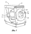
- the present centrifugal processor 10 has a cylindrical bowl 14 mounted within a housing 12.
- a cylindrical cassette rotor 18 is rotatably mounted within the bowl 14 .
- the back end of the rotor 18 is connected to a drive motor 16 , which spins the rotor within the bowl 14 .
- the workpieces 22 are held within the rotor 18 , in a wafer cassette 24 , as shown in Fig. 10, placed within the rotor 18 .
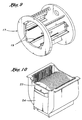
- a comb rotor 17 having combs 19 for directly holding the wafers 22 , as shown in Fig. 9, may be used.
- the techniques for holding wafers in the combs, or for holding the wafer cassette, in a rotor, as shown in Figs. 9 and 10, are well known in the art.
- the workpieces 22 may be semiconductor wafers, metal or glass disks, flat panels, lenses, or other flat media.
- One or more fluid spray manifolds such as manifolds 20 and 26 are positioned near the top of the bowl 14 .
- the wafers 22 or cassette 24 are loaded into the rotor 18 via a swing out door 30 .
- the manifolds may spray out liquid such as water, solvents, or acids, or gases, such as nitrogen.
- an ionizer 28 may also be provided.
- the rotor horizontal centerline or spin axis 52 is offset above and to one side of the bowl centerline 50 .
- the rotor spin axis is diagonally displaced from the bowl centerline 50 , by a distance D, and at an angle ⁇ from vertical.
- D is preferably about 1.3 cm and ⁇ is about 45°.
- E between the vertical centerline 56 of the rotor, and the vertical centerline 54 of the bowl 14 is about 0.9 cm.
- drain openings 41 are provided in a cluster 40 near the bottom of the bowl 14 .
- the openings 41 pass through the cylindrical sidewall of the bowl 14 .
- the openings 41 are arranged in a first row 42 staggered or offset from a second row 44 .
- the rotor 18 spins counter-clockwise in Figs. 1, 3 and 4.
- the cluster 40 of drain openings 41 is located at or between the 5 o'clock (30° counter-clockwise up from bottom center) and 6 o'clock (bottom center) positions.
- the motor 16 spins the rotor 18 .
- the rotor 16 is offset in a direction away from the openings 41. This offset position helps to avoid low pressure over the openings 41 , which reduces the tendency of the spinning rotor to draw fluid droplets up and away from the openings 41 .
- the drainage route out of the bowl 14 is made up of individual openings 41 , in contrast to the continuous drain channel used in prior designs, spent fluid drains more quickly from the bowl 14 .
- the combination of the offset rotor and openings 41 also allows spent fluid droplets which fall to the bottom of the bowl to exit the bowl under gravity via the openings, rather than splashing back onto and contaminating the wafers or workpieces.
- a drainage channel under the openings 41 similar to the channel shown in Fig. 2, catches the droplets and carries them to a drain.
- Figs. 6 and 8 show an alternative embodiment having a bowl 60 including alternating pairs of aligned drainage holes 62.
- the drainage holes are elliptical or oval-shaped.
- the major axis of each hole extends at an angle of about 30° to the major axes of the adjacent holes in the adjacent row.
- fluid droplets clinging to an edge of an opening 62 move toward the down wind (right side in Fig. 6) of the openings 62, and collect at the down wind radius of the hole.
- the force of gravity surpasses the surface tension adhesion forces and aerodynamic forces.
- the droplet then falls through the opening, to a collection pipe or channel on the outside of the bowl 14.
- a bowl depth R of about 280mm three rows of openings 62 are provided, with each row having 5 openings.
- the angles and dimensions S; T; U; V; W; and X are 15°; 29; 44; 22; and 57mm respectively, with the other dimensions shown proportionally to scale.
Abstract
Description
- The technical field of this invention is centrifugal processing equipment and methods used to process semiconductor wafers, photomasks, optical and glass disks, magnetic disks, flat panels, lenses or similar flat media.
- The production of semiconductor wafers, substrates and photomask plates used in the manufacture of semiconductor wafers, has typically utilized processing equipment in which various types of processing fluids are used to treat the wafers. One example of a semiconductor processor is a centrifugal rinser-dryer used to rinse acids, caustics, etchants and other processing fluids from wafers, photomask plates, and similar flat media.
- The rinser-dryers are also used to dry the rinsed units using a flow of heated gas, such as nitrogen, which is passed through the processing chamber after rinsing with the desired fluid. The wafers are spun during processing to provide more even distribution of the processing fluids across the wafer surfaces, and to assist in removal of rinsing liquids in preparation for drying.
- Other types of semiconductor processors include acid, solvent, and caustic treatment machines which spray or otherwise apply acids, solvents and caustics to the wafers or other flat media. Stripping processors are used to remove photoresist from the wafers. Other specific processing of semiconductors may require other types of chemicals. Many of these processes are performed in centrifugal processing machines to provide for even distribution of fluids over the wafer and to aid in removal of liquids.
- A primary problem in the production of semiconductors is particle contamination. Contaminant particles can affect the photographic processes used to transfer the chip layouts onto the wafers being processed into chips. Contaminants on the photomasks can cause deterioration of the image being transferred onto the wafer. The direct processing of the wafers themselves is even more susceptible to contamination because of the numerous processing steps involved and the risk at each stage that contaminating particles can become adhered to the surface of the wafer. Particle contamination causes a large number of the chips in a wafer to be defective. Thus it is very important to reduce contamination to increase yields.
- With the high resolution now made possible through newer semiconductor processing techniques, the effects of contaminants have become even more significant and problematic than in the past. Previously, contaminant particles smaller than 1 micron did not result in defects due to minimum feature sizes of 2 microns or more. However, now the feature size used in high density chip designs is substantially less, e.g., 0.18 micron. Even higher density chips with even smaller feature sizes are expected in the future. The move toward smaller feature size is compounding the contamination problem because of the greater difficulty in controlling smaller particles in the environment. If contaminants are present then substantial numbers of the resulting chips can be rendered defective and unusable, at substantial costs to the manufacturer.
- The causes of contaminating particles on wafer surfaces occurs from numerous sources. Each of the processing fluids used is necessarily impure to some small degree. The water used in processing is deionized to remove metallic ions and other impurities, but such supplies also contain some impurities. Centrifugal processing is advantageous because spinning the wafers or other flat media flings off fluid droplets. This helps to prevent contamination by "spotting" which occurs if fluid droplets on the wafer evaporate. It is also advantageous to have the used rinse water or fluids removed from the processing chamber as quickly as possible, to prevent recontamination.
- Centrifugal processors, such as spray solvent and spray acid processors, and spin rinser dryers, typically have a rotor which spins inside of a cylindrical processing chamber or bowl. The cylindrical rotor holds a removable cassette or non-removable combs which carry the wafers. The bowl typically has a drainage ditch or channel running from the front to the rear, near the bottom of the bowl, to drain fluids out of the bowl. These types of centrifugal processors have been used very successfully in semiconductor manufacturing.
- However, in these types of centrifugal processors, the spinning rotor, which is centered in the bowl, generates rapid counter-clockwise air movement within the bowl. This air movement hinders the clean drying or other processing operation of the centrifugal processor, as it tends to draw spent fluid droplets of e.g., water, solvent, or acid, up and around in the bowl, allowing droplets to be re-deposited on the wafers or other flat media. The air movement also tends to draw droplets away from the drainage channel, allowing them to be disadvantageously recycled back up and around the bowl.
- Accordingly, there remains a need in semiconductor manufacturing for improved centrifugal processing machines.
- US 0 471 541 A describes a washing-machine having a base formed with lower converging ends, n vertically-adjustable cylinders within the base, and a cover adapted to rest on the converging ends when in its lowered position.
- US 2 895 320 A describes a washing machine including a cabinet and a rotatable tub at an angle in said cabinet and provided with an inclined axis of rotation.
- The machine for cleaning clothes and the like disclosed in US 3 388 410 A includes a rotatable chamber adapted to receive clothes to be cleaned in a cleaning solution and means for rotating the chamber about its central axis at a relatively high speed.
- The closed cycle dry cleaning apparatus disclosed in US 3 410 118 A comprises a housing, an apertured basket rotatably mounted in said housing, and means for selectively rotating said basket.
- US 4 153 551 A describes a centrifuge having a drum to which a wobble or nutating motion is applied to discharge the centrifuged material over the edge of a wall of the perforated basket. The wobble or nutation is caused by tilting the axis of this wall relative to the axis rotation of the assembly.
- The present invention is directed to a centrifugal semiconductor wafer spray processor with a rotor contained within a bowl which is designed to better direct and scavenge fluids from the bowl. By doing so, a more complete process can be accomplished with less risk of contamination from spent fluid.
- The present invention provides a centrifugal semiconductor wafer spray processor as featured in independent claim. Preferred embodiments are described in the dependent claims.
- In a first separate aspect of the present invention, the centrifugal processor includes a rotor offset from the centerline of the bowl. The offset provides an area of lower fluid velocities. Thus, separation of entrained fluid droplets from the rotating air or gas flow is enhanced.
- In a second separate aspect of the present invention, the centrifugal processor includes drain openings in the form of staggered slots. The slots quickly remove spent fluid from the bowl and inhibit any re-entraining of the fluid into the air flow within the bowl.
- In a third separate aspect of the present invention, the slots of the second separate aspect include peripheries which are not perpendicular to the flow. With such a configuration, fluid droplets accumulate and more readily fall out of the bowl.
- In a fourth separate aspect of the present invention, any one or more of the foregoing separate aspects are contemplated to be combined to enhance removal of fluid droplets.
- Accordingly, an object of the present invention is to provide an improved centrifugal processor, which more effectively removes used fluid from the bowl, thereby reducing the potential for recontamination of the silicon wafers or other flat media.
-
- Fig. 1 is a perspective view of the centrifugal processor of the invention;
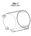
- Fig. 2 is a perspective view of a bowl of a prior art machine;
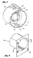
- Fig. 3 is a perspective view of the bowl of the present centrifugal processor shown in Fig. 1;
- Fig. 4 is a front elevation view of the bowl and rotor of the centrifugal processor shown in Fig. 1;
- Fig. 5 is a section view taken along line 5-5 of Fig. 4;
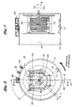
- Fig. 6 is a perspective view of a bowl according to a second embodiment of the invention;
- Fig. 7 is a section view taken along line 7-7 of Fig. 6;
- Fig. 8 is an enlarged detail of the openings shown in Figs. 6 and 7;
- Fig. 9 is a perspective view of a comb rotor having combs for directly holding wafers or other flat media; and
- Fig. 10 is a perspective view of a cassette holding wafers, with the cassette placeable into the rotor shown in Figs. 3 and 6.
- Turning now in detail to the drawings, as shown in Fig. 1, the present
centrifugal processor 10 has acylindrical bowl 14 mounted within ahousing 12. Referring to Figs. 1, 4 and 5, acylindrical cassette rotor 18 is rotatably mounted within thebowl 14. The back end of therotor 18 is connected to adrive motor 16, which spins the rotor within thebowl 14. Theworkpieces 22 are held within therotor 18, in awafer cassette 24, as shown in Fig. 10, placed within therotor 18. Alternatively, acomb rotor 17, havingcombs 19 for directly holding thewafers 22, as shown in Fig. 9, may be used. The techniques for holding wafers in the combs, or for holding the wafer cassette, in a rotor, as shown in Figs. 9 and 10, are well known in the art. Theworkpieces 22 may be semiconductor wafers, metal or glass disks, flat panels, lenses, or other flat media. - One or more fluid spray manifolds, such as
manifolds bowl 14. Thewafers 22 orcassette 24 are loaded into therotor 18 via a swing outdoor 30. The manifolds may spray out liquid such as water, solvents, or acids, or gases, such as nitrogen. Depending on the type of centrifugal processing performed, anionizer 28 may also be provided. - Referring to Figs. 4 and 5, wherein the illustrated features are drawn to scale, the rotor horizontal centerline or spin
axis 52 is offset above and to one side of thebowl centerline 50. As shown in Fig. 4, the rotor spin axis is diagonally displaced from thebowl centerline 50, by a distance D, and at an angle α from vertical. - In an embodiment having a bowl inside diameter of about 35 cm, D is preferably about 1.3 cm and α is about 45°. Correspondingly, the distance E between the
vertical centerline 56 of the rotor, and thevertical centerline 54 of thebowl 14 is about 0.9 cm. - Referring to Fig. 3,
drain openings 41 are provided in acluster 40 near the bottom of thebowl 14. Theopenings 41 pass through the cylindrical sidewall of thebowl 14. Theopenings 41 are arranged in afirst row 42 staggered or offset from asecond row 44. Therotor 18 spins counter-clockwise in Figs. 1, 3 and 4. Thecluster 40 ofdrain openings 41 is located at or between the 5 o'clock (30° counter-clockwise up from bottom center) and 6 o'clock (bottom center) positions. - In use, the
motor 16 spins therotor 18. As shown in Fig. 4, therotor 16 is offset in a direction away from theopenings 41. This offset position helps to avoid low pressure over theopenings 41, which reduces the tendency of the spinning rotor to draw fluid droplets up and away from theopenings 41. In addition, since the drainage route out of thebowl 14 is made up ofindividual openings 41, in contrast to the continuous drain channel used in prior designs, spent fluid drains more quickly from thebowl 14. The combination of the offset rotor andopenings 41 also allows spent fluid droplets which fall to the bottom of the bowl to exit the bowl under gravity via the openings, rather than splashing back onto and contaminating the wafers or workpieces. A drainage channel under theopenings 41, similar to the channel shown in Fig. 2, catches the droplets and carries them to a drain. - Figs. 6 and 8 show an alternative embodiment having a
bowl 60 including alternating pairs of aligned drainage holes 62. The drainage holes are elliptical or oval-shaped. The major axis of each hole extends at an angle of about 30° to the major axes of the adjacent holes in the adjacent row. As the spinningrotor 18 generates air movement in the direction A shown in Fig. 6, fluid droplets clinging to an edge of anopening 62 move toward the down wind (right side in Fig. 6) of theopenings 62, and collect at the down wind radius of the hole. As the droplets collect at the radius, and the volume of fluid builds up, the force of gravity surpasses the surface tension adhesion forces and aerodynamic forces. The droplet then falls through the opening, to a collection pipe or channel on the outside of thebowl 14. - As shown in Figs. 7 and 8, in a preferred embodiment having a bowl depth R of about 280mm, three rows of
openings 62 are provided, with each row having 5 openings. In the embodiment shown, the angles and dimensions S; T; U; V; W; and X are 15°; 29; 44; 22; and 57mm respectively, with the other dimensions shown proportionally to scale.
Claims (5)
- A centrifugal processor (10) having a housing (12), a bowl (14) within the housing (12), one or more spray manifolds (20, 26) for spraying liquids or gases into the bowl (14), and a rotor (18) rotatable within the bowl (14) for spinning the rotor (18) within the bowl (14), characterized by: the rotor (18) being rotatable within the bowl (14) about an axis offset from a central axis of the bowl (14).
- The processor (10) of claim 1, further characterized by multiple drain openings (41) in the bowl (14).
- The processor (10) of claim 1, further characterized by a flat media holder (24) within the rotor (18).
- The processor (10) of claim 3, further characterized by a flat media workpiece (22) in the flat media holder (24), the flat media workpiece (22) being selected from the group consisting of: silicon or other semiconductor material wafers, metal or glass disks, flat panels, replacement lenses used in cataract surgery, photomasks, optical disks, and magnetic disks.
- The processor (10) of claim 3, characterized in that the flat media holder (24) is a cassette within a cassette-holder within the rotor (18).
Applications Claiming Priority (3)
| Application Number | Priority Date | Filing Date | Title |
|---|---|---|---|
| US107878 | 1998-06-30 | ||
| US09/107,878 US6125863A (en) | 1998-06-30 | 1998-06-30 | Offset rotor flat media processor |
| PCT/US1999/013984 WO2000000301A1 (en) | 1998-06-30 | 1999-06-21 | Offset rotor flat media processor |
Publications (3)
| Publication Number | Publication Date |
|---|---|
| EP1115511A1 EP1115511A1 (en) | 2001-07-18 |
| EP1115511A4 EP1115511A4 (en) | 2005-04-20 |
| EP1115511B1 true EP1115511B1 (en) | 2007-04-11 |
Family
ID=22318945
Family Applications (1)
| Application Number | Title | Priority Date | Filing Date |
|---|---|---|---|
| EP99930500A Expired - Lifetime EP1115511B1 (en) | 1998-06-30 | 1999-06-21 | Offset rotor flat media processor |
Country Status (6)
| Country | Link |
|---|---|
| US (1) | US6125863A (en) |
| EP (1) | EP1115511B1 (en) |
| JP (1) | JP2002519856A (en) |
| AT (1) | ATE359132T1 (en) |
| DE (1) | DE69935795T2 (en) |
| WO (1) | WO2000000301A1 (en) |
Families Citing this family (15)
| Publication number | Priority date | Publication date | Assignee | Title |
|---|---|---|---|---|
| US6350322B1 (en) | 1997-03-21 | 2002-02-26 | Micron Technology, Inc. | Method of reducing water spotting and oxide growth on a semiconductor structure |
| US6516816B1 (en) * | 1999-04-08 | 2003-02-11 | Applied Materials, Inc. | Spin-rinse-dryer |
| US6691720B2 (en) * | 2001-07-16 | 2004-02-17 | Semitool, Inc. | Multi-process system with pivoting process chamber |
| US20040025901A1 (en) * | 2001-07-16 | 2004-02-12 | Semitool, Inc. | Stationary wafer spin/spray processor |
| US6895981B2 (en) * | 2002-07-19 | 2005-05-24 | Semitool, Inc. | Cross flow processor |
| JP2005534188A (en) * | 2002-07-26 | 2005-11-10 | アプライド マテリアルズ インコーポレイテッド | Hydrophilic components for spin dryers |
| US7289734B2 (en) * | 2002-12-24 | 2007-10-30 | Tropic Networks Inc. | Method and system for multi-level power management in an optical network |
| US20060201541A1 (en) * | 2005-03-11 | 2006-09-14 | Semiconductor Energy Laboratory Co., Ltd. | Cleaning-drying apparatus and cleaning-drying method |
| KR100829923B1 (en) * | 2006-08-30 | 2008-05-16 | 세메스 주식회사 | Spin head and method using the same for treating substrate |
| WO2009114043A1 (en) * | 2008-03-07 | 2009-09-17 | Automation Technology, Inc. | Solar wafer cleaning systems, apparatus and methods |
| US9421617B2 (en) | 2011-06-22 | 2016-08-23 | Tel Nexx, Inc. | Substrate holder |
| US8967935B2 (en) | 2011-07-06 | 2015-03-03 | Tel Nexx, Inc. | Substrate loader and unloader |
| AT515531B1 (en) * | 2014-09-19 | 2015-10-15 | Siconnex Customized Solutions Gmbh | Mounting system and feeding method for disc-shaped objects |
| WO2020010357A1 (en) | 2018-07-06 | 2020-01-09 | Oem Group, Llc | Systems and methods for a spray measurement apparatus |
| CN115228828B (en) * | 2022-09-20 | 2023-01-24 | 山东鲁西药业有限公司 | Medicine raw materials belt cleaning device |
Family Cites Families (87)
| Publication number | Priority date | Publication date | Assignee | Title |
|---|---|---|---|---|
| US28135A (en) * | 1860-05-01 | Aaron williamson | ||
| US193222A (en) * | 1877-07-17 | Improvement in steam dish-cleaners | ||
| US1035480A (en) * | 1907-10-09 | 1912-08-13 | Milton Schnaier | Area-drain. |
| US910882A (en) * | 1908-10-15 | 1909-01-26 | George Truesdell | Bottle-washing apparatus. |
| US1405243A (en) * | 1920-11-16 | 1922-01-31 | Claude E Wing | Dishwashing machine |
| US1793798A (en) * | 1928-07-05 | 1931-02-24 | Sarah B Harker | Dishwashing machine |
| US2225501A (en) * | 1938-06-04 | 1940-12-17 | James R Lapham | Machine for washing cream separator disks |
| US2699660A (en) * | 1946-05-23 | 1955-01-18 | Apex Electrical Mfg Co | Washing and extracting machine |
| US2573128A (en) * | 1947-04-05 | 1951-10-30 | Cavicchioli Mario | Device in dishwashing machine for recovering silverware and the like |
| US2677381A (en) * | 1950-05-25 | 1954-05-04 | Spray Blast Corp | Spray blast cleaning cabinet |
| US2684585A (en) * | 1951-08-01 | 1954-07-27 | Carl D Smith | Washing machine |
| US2669660A (en) * | 1951-10-27 | 1954-02-16 | Western Electric Co | Leak detecting apparatus |
| US2721566A (en) * | 1952-05-08 | 1955-10-25 | William E Brucker | Parts washer |
| US2675012A (en) * | 1952-10-18 | 1954-04-13 | Frank J Scales | Washing apparatus for automotive and machine parts and assmeblies |
| US3214026A (en) * | 1961-10-03 | 1965-10-26 | Borg Warner | Solvent recovery device |
| US3079286A (en) * | 1962-03-02 | 1963-02-26 | Detrex Chem Ind | Enclosed cold solvent spray cleaner |
| US3116744A (en) * | 1962-10-26 | 1964-01-07 | Earl E Hager | Washing machine for small articles |
| US3203434A (en) * | 1963-12-06 | 1965-08-31 | Western Electric Co | Chemical polishing machine |
| US3242934A (en) * | 1964-07-22 | 1966-03-29 | Heinricke Instr Co | Combination washer and drier |
| US3383255A (en) * | 1964-11-05 | 1968-05-14 | North American Rockwell | Planar etching of fused silica |
| US3341016A (en) * | 1965-08-23 | 1967-09-12 | Jens A Paasche | Spray booth |
| DE1477965A1 (en) * | 1965-10-08 | 1969-06-04 | Badische Maschinenfabrik Ag Se | Centrifugal blast machine |
| US3489608A (en) * | 1965-10-26 | 1970-01-13 | Kulicke & Soffa Ind Inc | Method and apparatus for treating semiconductor wafers |
| US3443567A (en) * | 1967-11-01 | 1969-05-13 | Howard L Moore | Automatic egg flat washer |
| US3607478A (en) * | 1967-12-14 | 1971-09-21 | Bosch Gmbh Robert | Method of treating semiconductor elements of circular outline |
| US3464429A (en) * | 1967-12-14 | 1969-09-02 | Henry B Ehrhardt | Automatic washer for small machine parts |
| US3526237A (en) * | 1968-05-08 | 1970-09-01 | Scott E Neill Jr | Filter cleaner |
| US3585668A (en) * | 1969-06-02 | 1971-06-22 | Bell Telephone Labor Inc | Brush cleaning apparatus for semiconductor slices |
| US3585128A (en) * | 1969-07-28 | 1971-06-15 | Gen Electric | Pre-wash scrap basket for dishwasher |
| US3727620A (en) * | 1970-03-18 | 1973-04-17 | Fluoroware Of California Inc | Rinsing and drying device |
| US3608567A (en) * | 1970-06-26 | 1971-09-28 | Scott E Neill Jr | Filter cleaning process and apparatuses |
| US3664872A (en) * | 1970-09-18 | 1972-05-23 | Western Electric Co | Method for scrubbing thin, fragile slices of material |
| US3748677A (en) * | 1970-09-18 | 1973-07-31 | Western Electric Co | Methods and apparatus for scrubbing thin, fragile slices of material |
| DE2125102A1 (en) * | 1971-05-19 | 1972-11-30 | Anton Huber Gmbh & Co Kg, 8050 Freising | Method and device for cleaning a number of small objects |
| US3756410A (en) * | 1971-11-08 | 1973-09-04 | Moody Aquamatic System Inc | Sewage disposal effluent purifier |
| US3769992A (en) * | 1971-12-06 | 1973-11-06 | Fluoroware Inc | Spray processing machine |
| US3808065A (en) * | 1972-02-28 | 1974-04-30 | Rca Corp | Method of polishing sapphire and spinel |
| US3760822A (en) * | 1972-03-22 | 1973-09-25 | A Evans | Machine for cleaning semiconductive wafers |
| US3804758A (en) * | 1972-03-29 | 1974-04-16 | Cosham Eng Design Ltd | Screen changer |
| US4027686A (en) * | 1973-01-02 | 1977-06-07 | Texas Instruments Incorporated | Method and apparatus for cleaning the surface of a semiconductor slice with a liquid spray of de-ionized water |
| US3964957A (en) * | 1973-12-19 | 1976-06-22 | Monsanto Company | Apparatus for processing semiconductor wafers |
| US3939514A (en) * | 1974-11-11 | 1976-02-24 | Kayex Corporation | Apparatus for cleaning thin, fragile wafers of a material |
| US3977926A (en) * | 1974-12-20 | 1976-08-31 | Western Electric Company, Inc. | Methods for treating articles |
| US3970471A (en) * | 1975-04-23 | 1976-07-20 | Western Electric Co., Inc. | Methods and apparatus for treating wafer-like articles |
| US3990462A (en) * | 1975-05-19 | 1976-11-09 | Fluoroware Systems Corporation | Substrate stripping and cleaning apparatus |
| JPS5271871A (en) * | 1975-12-11 | 1977-06-15 | Nec Corp | Washing apparatus |
| DE2710586C2 (en) * | 1977-03-11 | 1981-12-24 | Krauss-Maffei AG, 8000 München | Tumbling centrifuge |
| US4132567A (en) * | 1977-10-13 | 1979-01-02 | Fsi Corporation | Apparatus for and method of cleaning and removing static charges from substrates |
| US4208760A (en) * | 1977-12-19 | 1980-06-24 | Huestis Machine Corp. | Apparatus and method for cleaning wafers |
| DE2901643A1 (en) * | 1979-01-17 | 1980-07-31 | Krauss Maffei Ag | CENTRIFUGES PRODUCT ACCELERATOR |
| US4226642A (en) * | 1979-02-06 | 1980-10-07 | American Sterilizer Company | System providing for decontamination washing and/or biocidal treatment |
| US4286541A (en) * | 1979-07-26 | 1981-09-01 | Fsi Corporation | Applying photoresist onto silicon wafers |
| US4300581A (en) * | 1980-03-06 | 1981-11-17 | Thompson Raymon F | Centrifugal wafer processor |
| JPS587830A (en) * | 1981-07-08 | 1983-01-17 | Hitachi Ltd | Article washing method and device thererof |
| US4370992A (en) * | 1981-09-21 | 1983-02-01 | Abbott Laboratories | Washing apparatus for small parts |
| US4456022A (en) * | 1981-10-16 | 1984-06-26 | Roberts Donald E | Flatware washing machine |
| DE3223703C2 (en) * | 1982-06-25 | 1984-05-30 | M.A.N. Maschinenfabrik Augsburg-Nürnberg AG, 4200 Oberhausen | Gas-locked shaft seal with radial sealing gap |
| US4440185A (en) * | 1982-08-18 | 1984-04-03 | Wiltse Dean P | Support stand for a food slicer |
| JPS6014244A (en) * | 1983-07-06 | 1985-01-24 | Fujitsu Ltd | Washing device for mask |
| US4982753A (en) * | 1983-07-26 | 1991-01-08 | National Semiconductor Corporation | Wafer etching, cleaning and stripping apparatus |
| US4536845A (en) * | 1983-08-31 | 1985-08-20 | Culligan International Company | Self-programmable controller for water conditioner recharging |
| US4571850A (en) * | 1984-05-17 | 1986-02-25 | The Fluorocarbon Company | Centrifugal wafer processor |
| DE8430403U1 (en) * | 1984-10-16 | 1985-04-25 | Gebr. Steimel, 5202 Hennef | CENTERING DEVICE |
| JPS61164226A (en) * | 1985-01-17 | 1986-07-24 | Toshiba Ceramics Co Ltd | Washing device for semiconductor wafer |
| JPS61178187U (en) * | 1985-04-26 | 1986-11-06 | ||
| US4682614A (en) * | 1985-07-26 | 1987-07-28 | Fsi Corporation | Wafer processing machine |
| US4753258A (en) * | 1985-08-06 | 1988-06-28 | Aigo Seiichiro | Treatment basin for semiconductor material |
| US4745422A (en) * | 1985-11-18 | 1988-05-17 | Kabushiki Kaisha Toshiba | Automatic developing apparatus |
| US4731154A (en) * | 1986-06-23 | 1988-03-15 | The Dow Chemical Company | Method and apparatus for quantitative measurement of organic contaminants remaining on cleaned surfaces |
| JPS6314434A (en) * | 1986-07-04 | 1988-01-21 | Dainippon Screen Mfg Co Ltd | Substrate surface processing and equipment therefor |
| US4788994A (en) * | 1986-08-13 | 1988-12-06 | Dainippon Screen Mfg. Co. | Wafer holding mechanism |
| US4828660A (en) * | 1986-10-06 | 1989-05-09 | Athens Corporation | Method and apparatus for the continuous on-site chemical reprocessing of ultrapure liquids |
| US5022419A (en) * | 1987-04-27 | 1991-06-11 | Semitool, Inc. | Rinser dryer system |
| US5095927A (en) * | 1987-04-27 | 1992-03-17 | Semitool, Inc. | Semiconductor processor gas-liquid separation |
| DE3815018A1 (en) * | 1987-05-06 | 1988-12-01 | Dan Science Co | CARRIER CLEANING AND DRYING DEVICE |
| JPH069499Y2 (en) * | 1987-06-23 | 1994-03-09 | 黒谷 信子 | Draining device for semiconductor materials |
| JPH01111338A (en) * | 1987-10-24 | 1989-04-28 | Sony Corp | Cleaning and cleaning apparatus |
| AT389959B (en) * | 1987-11-09 | 1990-02-26 | Sez Semiconduct Equip Zubehoer | DEVICE FOR SETTING DISC-SHAPED OBJECTS, ESPECIALLY SILICONE DISC |
| JPH0264646A (en) * | 1988-08-31 | 1990-03-05 | Toshiba Corp | Developing method for resist pattern and developing device using the same |
| US5069236A (en) * | 1990-03-07 | 1991-12-03 | Pathway Systems, Inc. | Method and apparatus for cleaning disks |
| US5027841A (en) * | 1990-04-24 | 1991-07-02 | Electronic Controls Design, Inc. | Apparatus to clean printed circuit boards |
| US5000208A (en) * | 1990-06-21 | 1991-03-19 | Micron Technology, Inc. | Wafer rinser/dryer |
| US5232328A (en) * | 1991-03-05 | 1993-08-03 | Semitool, Inc. | Robot loadable centrifugal semiconductor processor with extendible rotor |
| US5174045A (en) * | 1991-05-17 | 1992-12-29 | Semitool, Inc. | Semiconductor processor with extendible receiver for handling multiple discrete wafers without wafer carriers |
| JP2877216B2 (en) * | 1992-10-02 | 1999-03-31 | 東京エレクトロン株式会社 | Cleaning equipment |
| US5784797A (en) * | 1994-04-28 | 1998-07-28 | Semitool, Inc. | Carrierless centrifugal semiconductor processing system |
| US5664337A (en) * | 1996-03-26 | 1997-09-09 | Semitool, Inc. | Automated semiconductor processing systems |
-
1998
- 1998-06-30 US US09/107,878 patent/US6125863A/en not_active Expired - Lifetime
-
1999
- 1999-06-21 DE DE69935795T patent/DE69935795T2/en not_active Expired - Lifetime
- 1999-06-21 EP EP99930500A patent/EP1115511B1/en not_active Expired - Lifetime
- 1999-06-21 WO PCT/US1999/013984 patent/WO2000000301A1/en active IP Right Grant
- 1999-06-21 JP JP2000556884A patent/JP2002519856A/en active Pending
- 1999-06-21 AT AT99930500T patent/ATE359132T1/en active
Also Published As
| Publication number | Publication date |
|---|---|
| US6125863A (en) | 2000-10-03 |
| ATE359132T1 (en) | 2007-05-15 |
| DE69935795T2 (en) | 2007-12-27 |
| EP1115511A4 (en) | 2005-04-20 |
| JP2002519856A (en) | 2002-07-02 |
| DE69935795D1 (en) | 2007-05-24 |
| EP1115511A1 (en) | 2001-07-18 |
| WO2000000301A1 (en) | 2000-01-06 |
Similar Documents
| Publication | Publication Date | Title |
|---|---|---|
| EP1115511B1 (en) | Offset rotor flat media processor | |
| JP3556043B2 (en) | Substrate drying equipment | |
| US7472713B2 (en) | Substrate processing apparatus | |
| JPH1092784A (en) | Wafer treatment equipment and wafer treatment method | |
| JP2008034779A (en) | Method and equipment for processing substrate | |
| US6062239A (en) | Cross flow centrifugal processor | |
| US7678199B2 (en) | Substrate cleaning method | |
| JP3713447B2 (en) | Development processing equipment | |
| JPH0878368A (en) | Work treating method and apparatus | |
| JP4457046B2 (en) | Substrate processing equipment | |
| JPH10189511A (en) | Wafer cleaning device | |
| JP4325831B2 (en) | Substrate processing apparatus, rotating plate provided in substrate processing apparatus, and method for cleaning surrounding member | |
| KR100998849B1 (en) | Single type cleaning apparatus for substrate | |
| KR100408114B1 (en) | Substrate processing apparatus | |
| KR20090131207A (en) | Spin chuck and apparatus and method for cleaning substrate having the same | |
| JP2000114219A (en) | Substrate-processing device | |
| KR101018963B1 (en) | Substrate processing apparatus and cleaning method | |
| JP2000208466A (en) | Method and apparatus for treating substrate | |
| JP2916409B2 (en) | Spin cleaning method and apparatus therefor | |
| JP2001217218A (en) | Device and method for treating wafer | |
| JP2002261065A (en) | Spin processor | |
| JP4347765B2 (en) | Substrate processing equipment | |
| KR100830394B1 (en) | Spin coating apparatus | |
| KR100983759B1 (en) | Apparatus for cleaning substrate | |
| KR100885242B1 (en) | Apparatus for treating substrates, and method for treating substrates using the same |
Legal Events
| Date | Code | Title | Description |
|---|---|---|---|
| PUAI | Public reference made under article 153(3) epc to a published international application that has entered the european phase |
Free format text: ORIGINAL CODE: 0009012 |
|
| 17P | Request for examination filed |
Effective date: 20010129 |
|
| AK | Designated contracting states |
Kind code of ref document: A1 Designated state(s): AT BE CH CY DE DK ES FI FR GB GR IE IT LI LU MC NL PT SE |
|
| A4 | Supplementary search report drawn up and despatched |
Effective date: 20050304 |
|
| GRAP | Despatch of communication of intention to grant a patent |
Free format text: ORIGINAL CODE: EPIDOSNIGR1 |
|
| GRAS | Grant fee paid |
Free format text: ORIGINAL CODE: EPIDOSNIGR3 |
|
| GRAA | (expected) grant |
Free format text: ORIGINAL CODE: 0009210 |
|
| AK | Designated contracting states |
Kind code of ref document: B1 Designated state(s): AT BE CH CY DE DK ES FI FR GB GR IE IT LI LU MC NL PT SE |
|
| PG25 | Lapsed in a contracting state [announced via postgrant information from national office to epo] |
Ref country code: LI Free format text: LAPSE BECAUSE OF FAILURE TO SUBMIT A TRANSLATION OF THE DESCRIPTION OR TO PAY THE FEE WITHIN THE PRESCRIBED TIME-LIMIT Effective date: 20070411 Ref country code: FI Free format text: LAPSE BECAUSE OF FAILURE TO SUBMIT A TRANSLATION OF THE DESCRIPTION OR TO PAY THE FEE WITHIN THE PRESCRIBED TIME-LIMIT Effective date: 20070411 Ref country code: CH Free format text: LAPSE BECAUSE OF FAILURE TO SUBMIT A TRANSLATION OF THE DESCRIPTION OR TO PAY THE FEE WITHIN THE PRESCRIBED TIME-LIMIT Effective date: 20070411 |
|
| REG | Reference to a national code |
Ref country code: GB Ref legal event code: FG4D |
|
| REG | Reference to a national code |
Ref country code: CH Ref legal event code: EP |
|
| REG | Reference to a national code |
Ref country code: IE Ref legal event code: FG4D |
|
| REF | Corresponds to: |
Ref document number: 69935795 Country of ref document: DE Date of ref document: 20070524 Kind code of ref document: P |
|
| PG25 | Lapsed in a contracting state [announced via postgrant information from national office to epo] |
Ref country code: SE Free format text: LAPSE BECAUSE OF FAILURE TO SUBMIT A TRANSLATION OF THE DESCRIPTION OR TO PAY THE FEE WITHIN THE PRESCRIBED TIME-LIMIT Effective date: 20070711 |
|
| PG25 | Lapsed in a contracting state [announced via postgrant information from national office to epo] |
Ref country code: ES Free format text: LAPSE BECAUSE OF FAILURE TO SUBMIT A TRANSLATION OF THE DESCRIPTION OR TO PAY THE FEE WITHIN THE PRESCRIBED TIME-LIMIT Effective date: 20070722 |
|
| PG25 | Lapsed in a contracting state [announced via postgrant information from national office to epo] |
Ref country code: PT Free format text: LAPSE BECAUSE OF FAILURE TO SUBMIT A TRANSLATION OF THE DESCRIPTION OR TO PAY THE FEE WITHIN THE PRESCRIBED TIME-LIMIT Effective date: 20070911 |
|
| NLV1 | Nl: lapsed or annulled due to failure to fulfill the requirements of art. 29p and 29m of the patents act | ||
| REG | Reference to a national code |
Ref country code: CH Ref legal event code: PL |
|
| EN | Fr: translation not filed | ||
| PG25 | Lapsed in a contracting state [announced via postgrant information from national office to epo] |
Ref country code: BE Free format text: LAPSE BECAUSE OF FAILURE TO SUBMIT A TRANSLATION OF THE DESCRIPTION OR TO PAY THE FEE WITHIN THE PRESCRIBED TIME-LIMIT Effective date: 20070411 |
|
| PG25 | Lapsed in a contracting state [announced via postgrant information from national office to epo] |
Ref country code: NL Free format text: LAPSE BECAUSE OF FAILURE TO SUBMIT A TRANSLATION OF THE DESCRIPTION OR TO PAY THE FEE WITHIN THE PRESCRIBED TIME-LIMIT Effective date: 20070411 Ref country code: MC Free format text: LAPSE BECAUSE OF NON-PAYMENT OF DUE FEES Effective date: 20070630 Ref country code: DK Free format text: LAPSE BECAUSE OF FAILURE TO SUBMIT A TRANSLATION OF THE DESCRIPTION OR TO PAY THE FEE WITHIN THE PRESCRIBED TIME-LIMIT Effective date: 20070411 |
|
| PLBE | No opposition filed within time limit |
Free format text: ORIGINAL CODE: 0009261 |
|
| STAA | Information on the status of an ep patent application or granted ep patent |
Free format text: STATUS: NO OPPOSITION FILED WITHIN TIME LIMIT |
|
| 26N | No opposition filed |
Effective date: 20080114 |
|
| PG25 | Lapsed in a contracting state [announced via postgrant information from national office to epo] |
Ref country code: IT Free format text: LAPSE BECAUSE OF FAILURE TO SUBMIT A TRANSLATION OF THE DESCRIPTION OR TO PAY THE FEE WITHIN THE PRESCRIBED TIME-LIMIT Effective date: 20070411 Ref country code: GR Free format text: LAPSE BECAUSE OF FAILURE TO SUBMIT A TRANSLATION OF THE DESCRIPTION OR TO PAY THE FEE WITHIN THE PRESCRIBED TIME-LIMIT Effective date: 20070712 Ref country code: FR Free format text: LAPSE BECAUSE OF FAILURE TO SUBMIT A TRANSLATION OF THE DESCRIPTION OR TO PAY THE FEE WITHIN THE PRESCRIBED TIME-LIMIT Effective date: 20071207 |
|
| PG25 | Lapsed in a contracting state [announced via postgrant information from national office to epo] |
Ref country code: IE Free format text: LAPSE BECAUSE OF NON-PAYMENT OF DUE FEES Effective date: 20070621 |
|
| PG25 | Lapsed in a contracting state [announced via postgrant information from national office to epo] |
Ref country code: FR Free format text: LAPSE BECAUSE OF FAILURE TO SUBMIT A TRANSLATION OF THE DESCRIPTION OR TO PAY THE FEE WITHIN THE PRESCRIBED TIME-LIMIT Effective date: 20070411 |
|
| PG25 | Lapsed in a contracting state [announced via postgrant information from national office to epo] |
Ref country code: CY Free format text: LAPSE BECAUSE OF FAILURE TO SUBMIT A TRANSLATION OF THE DESCRIPTION OR TO PAY THE FEE WITHIN THE PRESCRIBED TIME-LIMIT Effective date: 20070411 |
|
| PG25 | Lapsed in a contracting state [announced via postgrant information from national office to epo] |
Ref country code: LU Free format text: LAPSE BECAUSE OF NON-PAYMENT OF DUE FEES Effective date: 20070621 |
|
| REG | Reference to a national code |
Ref country code: DE Ref legal event code: R082 Ref document number: 69935795 Country of ref document: DE Representative=s name: VIERING, JENTSCHURA & PARTNER, DE |
|
| REG | Reference to a national code |
Ref country code: GB Ref legal event code: 732E Free format text: REGISTERED BETWEEN 20120802 AND 20120808 |
|
| REG | Reference to a national code |
Ref country code: DE Ref legal event code: R082 Ref document number: 69935795 Country of ref document: DE Representative=s name: VIERING, JENTSCHURA & PARTNER, DE Effective date: 20120801 Ref country code: DE Ref legal event code: R081 Ref document number: 69935795 Country of ref document: DE Owner name: APPLIED MATERIALS, INC. (N.D.GES.D. STAATES DE, US Free format text: FORMER OWNER: SEMITOOL, INC., KALISPELL, MONT., US Effective date: 20120801 Ref country code: DE Ref legal event code: R081 Ref document number: 69935795 Country of ref document: DE Owner name: APPLIED MATERIALS, INC. (N.D.GES.D. STAATES DE, US Free format text: FORMER OWNER: SEMITOOL, INC., KALISPELL, US Effective date: 20120801 |
|
| REG | Reference to a national code |
Ref country code: AT Ref legal event code: PC Ref document number: 359132 Country of ref document: AT Kind code of ref document: T Owner name: APPLIED MATERIALS, INC., US Effective date: 20120913 |
|
| PGFP | Annual fee paid to national office [announced via postgrant information from national office to epo] |
Ref country code: AT Payment date: 20120525 Year of fee payment: 14 |
|
| PGFP | Annual fee paid to national office [announced via postgrant information from national office to epo] |
Ref country code: GB Payment date: 20130529 Year of fee payment: 15 |
|
| PGFP | Annual fee paid to national office [announced via postgrant information from national office to epo] |
Ref country code: DE Payment date: 20130628 Year of fee payment: 15 |
|
| REG | Reference to a national code |
Ref country code: DE Ref legal event code: R119 Ref document number: 69935795 Country of ref document: DE |
|
| REG | Reference to a national code |
Ref country code: AT Ref legal event code: MM01 Ref document number: 359132 Country of ref document: AT Kind code of ref document: T Effective date: 20140621 |
|
| GBPC | Gb: european patent ceased through non-payment of renewal fee |
Effective date: 20140621 |
|
| REG | Reference to a national code |
Ref country code: DE Ref legal event code: R119 Ref document number: 69935795 Country of ref document: DE Effective date: 20150101 |
|
| PG25 | Lapsed in a contracting state [announced via postgrant information from national office to epo] |
Ref country code: DE Free format text: LAPSE BECAUSE OF NON-PAYMENT OF DUE FEES Effective date: 20150101 |
|
| PG25 | Lapsed in a contracting state [announced via postgrant information from national office to epo] |
Ref country code: GB Free format text: LAPSE BECAUSE OF NON-PAYMENT OF DUE FEES Effective date: 20140621 Ref country code: AT Free format text: LAPSE BECAUSE OF NON-PAYMENT OF DUE FEES Effective date: 20140621 |