EP1119056A2 - Semiconductor for device and method of fabrication - Google Patents
Semiconductor for device and method of fabrication Download PDFInfo
- Publication number
- EP1119056A2 EP1119056A2 EP01300349A EP01300349A EP1119056A2 EP 1119056 A2 EP1119056 A2 EP 1119056A2 EP 01300349 A EP01300349 A EP 01300349A EP 01300349 A EP01300349 A EP 01300349A EP 1119056 A2 EP1119056 A2 EP 1119056A2
- Authority
- EP
- European Patent Office
- Prior art keywords
- insulating layer
- layer
- active region
- over
- bond pad
- Prior art date
- Legal status (The legal status is an assumption and is not a legal conclusion. Google has not performed a legal analysis and makes no representation as to the accuracy of the status listed.)
- Withdrawn
Links
- 239000004065 semiconductor Substances 0.000 title claims abstract description 21
- 238000004519 manufacturing process Methods 0.000 title claims abstract description 11
- 238000000034 method Methods 0.000 claims abstract description 28
- 229910052751 metal Inorganic materials 0.000 claims abstract description 19
- 239000002184 metal Substances 0.000 claims abstract description 19
- 239000000758 substrate Substances 0.000 claims abstract description 18
- 238000000151 deposition Methods 0.000 claims abstract description 13
- 230000008021 deposition Effects 0.000 claims abstract description 10
- 238000010884 ion-beam technique Methods 0.000 claims abstract description 4
- 239000000463 material Substances 0.000 claims description 8
- 229910052737 gold Inorganic materials 0.000 claims description 7
- GWEVSGVZZGPLCZ-UHFFFAOYSA-N Titan oxide Chemical compound O=[Ti]=O GWEVSGVZZGPLCZ-UHFFFAOYSA-N 0.000 claims description 6
- 230000003287 optical effect Effects 0.000 claims description 5
- 239000000203 mixture Substances 0.000 claims description 4
- 239000004642 Polyimide Substances 0.000 claims description 3
- VYPSYNLAJGMNEJ-UHFFFAOYSA-N Silicium dioxide Chemical compound O=[Si]=O VYPSYNLAJGMNEJ-UHFFFAOYSA-N 0.000 claims description 3
- PNEYBMLMFCGWSK-UHFFFAOYSA-N aluminium oxide Inorganic materials [O-2].[O-2].[O-2].[Al+3].[Al+3] PNEYBMLMFCGWSK-UHFFFAOYSA-N 0.000 claims description 3
- PMSZNCMIJVNSPB-UHFFFAOYSA-N bis(ethenyl)silicon Chemical compound C=C[Si]C=C PMSZNCMIJVNSPB-UHFFFAOYSA-N 0.000 claims description 3
- 229910052804 chromium Inorganic materials 0.000 claims description 3
- 229910052593 corundum Inorganic materials 0.000 claims description 3
- 238000005566 electron beam evaporation Methods 0.000 claims description 3
- 229920001721 polyimide Polymers 0.000 claims description 3
- 229920001343 polytetrafluoroethylene Polymers 0.000 claims description 3
- 229910052814 silicon oxide Inorganic materials 0.000 claims description 3
- PBCFLUZVCVVTBY-UHFFFAOYSA-N tantalum pentoxide Inorganic materials O=[Ta](=O)O[Ta](=O)=O PBCFLUZVCVVTBY-UHFFFAOYSA-N 0.000 claims description 3
- 229910001845 yogo sapphire Inorganic materials 0.000 claims description 3
- 238000009792 diffusion process Methods 0.000 claims description 2
- 239000012535 impurity Substances 0.000 claims description 2
- 229910052759 nickel Inorganic materials 0.000 claims 2
- 230000008020 evaporation Effects 0.000 claims 1
- 238000001704 evaporation Methods 0.000 claims 1
- 238000000059 patterning Methods 0.000 claims 1
- 238000004544 sputter deposition Methods 0.000 description 7
- 239000003989 dielectric material Substances 0.000 description 6
- CFAKWWQIUFSQFU-UHFFFAOYSA-N 2-hydroxy-3-methylcyclopent-2-en-1-one Chemical compound CC1=C(O)C(=O)CC1 CFAKWWQIUFSQFU-UHFFFAOYSA-N 0.000 description 4
- 239000002318 adhesion promoter Substances 0.000 description 3
- 239000000969 carrier Substances 0.000 description 3
- 238000005530 etching Methods 0.000 description 3
- ARXJGSRGQADJSQ-UHFFFAOYSA-N 1-methoxypropan-2-ol Chemical compound COCC(C)O ARXJGSRGQADJSQ-UHFFFAOYSA-N 0.000 description 2
- 239000001837 2-hydroxy-3-methylcyclopent-2-en-1-one Substances 0.000 description 2
- 239000006096 absorbing agent Substances 0.000 description 2
- 238000000206 photolithography Methods 0.000 description 2
- 239000000126 substance Substances 0.000 description 2
- VATRWWPJWVCZTA-UHFFFAOYSA-N 3-oxo-n-[2-(trifluoromethyl)phenyl]butanamide Chemical compound CC(=O)CC(=O)NC1=CC=CC=C1C(F)(F)F VATRWWPJWVCZTA-UHFFFAOYSA-N 0.000 description 1
- 229910000530 Gallium indium arsenide Inorganic materials 0.000 description 1
- 239000004809 Teflon Substances 0.000 description 1
- 229920006362 Teflon® Polymers 0.000 description 1
- NOZAQBYNLKNDRT-UHFFFAOYSA-N [diacetyloxy(ethenyl)silyl] acetate Chemical compound CC(=O)O[Si](OC(C)=O)(OC(C)=O)C=C NOZAQBYNLKNDRT-UHFFFAOYSA-N 0.000 description 1
- 229910052793 cadmium Inorganic materials 0.000 description 1
- 230000015556 catabolic process Effects 0.000 description 1
- 238000006243 chemical reaction Methods 0.000 description 1
- 238000006731 degradation reaction Methods 0.000 description 1
- 239000008367 deionised water Substances 0.000 description 1
- 229910021641 deionized water Inorganic materials 0.000 description 1
- 238000001312 dry etching Methods 0.000 description 1
- 230000000694 effects Effects 0.000 description 1
- 238000010894 electron beam technology Methods 0.000 description 1
- 125000005842 heteroatom Chemical group 0.000 description 1
- 238000001659 ion-beam spectroscopy Methods 0.000 description 1
- 150000002500 ions Chemical class 0.000 description 1
- 230000007774 longterm Effects 0.000 description 1
- 239000002923 metal particle Substances 0.000 description 1
- 238000001465 metallisation Methods 0.000 description 1
- 150000002739 metals Chemical class 0.000 description 1
- 229920002120 photoresistant polymer Polymers 0.000 description 1
- 238000009987 spinning Methods 0.000 description 1
- 238000010561 standard procedure Methods 0.000 description 1
- 239000007858 starting material Substances 0.000 description 1
- XLYOFNOQVPJJNP-UHFFFAOYSA-N water Chemical compound O XLYOFNOQVPJJNP-UHFFFAOYSA-N 0.000 description 1
- 229910052725 zinc Inorganic materials 0.000 description 1
Images


Classifications
-
- H—ELECTRICITY
- H01—ELECTRIC ELEMENTS
- H01L—SEMICONDUCTOR DEVICES NOT COVERED BY CLASS H10
- H01L31/00—Semiconductor devices sensitive to infrared radiation, light, electromagnetic radiation of shorter wavelength or corpuscular radiation and specially adapted either for the conversion of the energy of such radiation into electrical energy or for the control of electrical energy by such radiation; Processes or apparatus specially adapted for the manufacture or treatment thereof or of parts thereof; Details thereof
- H01L31/02—Details
- H01L31/0224—Electrodes
- H01L31/022408—Electrodes for devices characterised by at least one potential jump barrier or surface barrier
-
- H—ELECTRICITY
- H01—ELECTRIC ELEMENTS
- H01L—SEMICONDUCTOR DEVICES NOT COVERED BY CLASS H10
- H01L2924/00—Indexing scheme for arrangements or methods for connecting or disconnecting semiconductor or solid-state bodies as covered by H01L24/00
- H01L2924/0001—Technical content checked by a classifier
- H01L2924/0002—Not covered by any one of groups H01L24/00, H01L24/00 and H01L2224/00
Definitions
- This invention relates to semiconductor devices, for example, optical semiconductor devices such as photodetectors.
- Electrodetectors often include a wire bond for providing electrical connection to the active regions of the device. Since pressure and ultrasonic energy are applied to effect the bond, the wire bonding process can lead to damage to the device resulting in such undesired characteristics as increased leakage current. In order to avoid this problem, it has been proposed to provide the wire bond pad at some portion away from the active area.
- Such bond sites are desirably formed in a manner which keeps additional capacitance to a minimum. This is of particular significance for high speed devices. It is known that capacitance is a function of the area of the pad, the dielectric constant of the insulating layer over which the pad is formed, and the thickness of the insulating layer. Therefore, one of the design criteria is to use an insulating layer with as low a dielectric constant as possible (known in the art as low k dielectric material) which can be applied with an adequate thickness. Desirably, the dielectric constant is no greater than 3 and the thickness is at least 4 ⁇ m.
- low k dielectric materials however, presents additional problems in the fabrication of the devices.
- metals generally adhere poorly to the low k dielectrics and conventional wire bonding techniques utilizing ultrasonic energy leads to low yielding manufacturing processes.
- metal deposition can be effected by sputtering to alleviate the metal adhesion problem, the simple and convenient method of a lift-off process to define metal patterns is not compatible with common sputtering processes.
- conventional sputtering is employed to deposit metal, often a conductive interface is produced on the whole surface of the low k dielectric (through a chemical reaction of energetic metal particles) and hence making it virtually impossible to devise a suitable manufacturing process to define a confined metal bond pad.
- bond pads are thick (2-4 ⁇ m) and hence makes sputtering an unattractive method of manufacturing as compared to conventional electron beam evaporation which is known in the art as having much higher deposition rates.
- substrate temperature may use rise high enough to cause surface degradation of low k dielectrics and eventually lead to potential long term reliability problems.
- the invention in accordance with one aspect is a semiconductor device including a semiconductor substrate, an active region in the substrate, a first low dielectric constant insulating layer formed over at least a portion of the substrate, a second insulating layer formed over at least a portion of the first insulating layer, and a bond pad formed over the second insulating layer and electrically contacting the active region.
- the invention in accordance with another aspect is a method of fabricating a semiconductor device including the steps of forming an active region in a semiconductor substrate, forming a first low dielectric constant insulating layer over at least a portion of the substrate, forming a second insulating layer over at least a portion of the first layer by deposition at a temperature no greater then 200°C, and forming a bond pad over the second insulating layer.
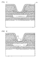
- Figs 1-7 illustrate the fabrication of a photodetector using principles of the invention. It will be appreciated that the invention is not limited to photodetectors, but can be applied to any semiconductor device where reduced capacitance is desirable.
- Fig 1 illustrates a typical starting material for the illustrative process.
- a semiconductor body, 10, preferably comprising n-type InP is provided, upon which are successively grown epitaxial layers, 11-13.
- the body, 10, and the layers, 11-13 are all considered as part of the semiconductor substrate.
- the layer, 11, was an undoped InP buffer layer with a thickness of approximately 1.5 microns.
- the layer, 12, was an undoped InGaAs absorber layer with a thickness of 2-5 microns.
- the layer, 13, was an undoped InP or InGaAsP contact layer with a thickness of approximately 0.5 microns.
- Such layers are standard for PIN photodiodes.
- a dielectric layer, 14, in this example SiN was deposited over the substrate and patterned by standard photolithographic techniques to form an opening, 30, therein.
- the active region is the region of the semiconductor device which includes a homo or hetero junction of opposite conductivity types.
- free carriers are produced in the active region by incident light and provide an electrical read-out.
- free carriers are produced by applying an electrical bin to the device and the carriers recombine to produce light in the active region.
- the preferred process continues with the deposition of an adhesion promoter, 18, over the dielectric layer, 16, and contact, 17, as shown in Fig 4.
- the adhesion promoter was vinyltriacetoxy silane dissolved in 1-methoxy-2-propanol (sold by Dow Chemical under the designation "AP3000") which was deposited by spinning.
- the low k dielectric was B-staged divinyl silane bisbenzocylobutane which is sold by Dow Chemical under the designation Cyclotene (TM). This material is advantageous since it can be spun-on the structure to a thickness of 5-10 microns.
- the dielectric constant of the material was approximately 2.56.
- any organic insulating layer with a dielectric constant less than 3 can be utilized.
- polyimide or polytetra fluroethylene (Teflon) could be employed.
- An opening, 31, was formed in the dielectric layer, 19, and adhesion promoter, 18, by exposure of the layer, 19, through a mask (not shown) and then developing with a suitable developer such as dipropylene glycol dimethyl ether to expose the underlying contact, 17.
- a suitable developer such as dipropylene glycol dimethyl ether
- this particular Cyclotene is a photosensitive material.
- other dielectrics which are not photosensitive can be employed, in which case, a separate patterned photoresist layer could be deposited over the dielectric followed by subtractive etching to define the opening, 31.
- an additional insulating layer, 20, was preferably deposited over the low k insulating layer, 19, and the exposed portion of the contact, 17.
- the layer is deposited at a temperature of less than 200 deg C so that the low k material does not degrade.
- ion beam assistance deposition which is described, for example in U.S. Patent No. 5,802,091. Briefly, such a deposition involved placing the structure in an evacuated chamber with a crucible containing oxide evaporatant which is impinged with an electron beam. The resulting vapor from the crucible was incident on the surface of the low k dielectric layer, 19, and contact, 17.
- the thickness of the layer, 20, was preferably within the range 1000 to 3000 ⁇ .
- the insulating layer, 20 was selectively etched to expose a portion of the underlying contact, 17.
- Standard photolithography was employed followed by etching.
- a convenient etchant comprises 1:10 HF and deionized water. It is understood that other methods of etching, e.g., dry etching are also possible.
- a metal stack, 21, was deposited over the insulating layer, 20, and the exposed portion of the contact, 17, so as to establish ohmic contact to the active region, 15, of the semiconductor.
- the metal stack can be, for example, Ti/Pt/Au, Cr/Pt/An, Ni/Pt/Au or Al/Pt/Au.
- the layer, 21 was deposited by electron beam evaporation to a total thickness within the range 3 ⁇ m to 4 ⁇ m.
- the presence of the insulating layer, 20, resulted in excellent adhesion of the metal stack, 21.
- the metal stack 21 was defined by a lift-off process which would not be used if the metal was deposited by sputtering.
- the metal layer, 21, comprises a contact portion, 22, overlying the active region, 15, and a bond pad portion, 23, which overlies the insulating layers, 19 and 20, and is laterally displaced from the area above the active region.
- This configuration permits a wire bond (not shown) to be made to the bond pad portion without the risk of damaging the active region.
Abstract
The invention is a semiconductor device and method of fabricating the device. The
device includes a semiconductor substrate (10-13) with an active region (15), and a low dielectric
constant insulating layer (19) formed over the substrate. An additional insulating layer (20) is
formed over the low dielectric constant layer by a low temperature deposition, such as ion beam
assistance deposition. A metal layer (21) can then be formed over the additional layer using lift-off
techniques. The metal layer can be patterned to form a bond pad (23) which may be displaced
from the area over the active region. Wire bonds can be made on the bond pad using ultrasonic
energy.
Description
- This invention relates to semiconductor devices, for example, optical semiconductor devices such as photodetectors.
- Semiconductor devices, such as photodetectors, often include a wire bond for providing electrical connection to the active regions of the device. Since pressure and ultrasonic energy are applied to effect the bond, the wire bonding process can lead to damage to the device resulting in such undesired characteristics as increased leakage current. In order to avoid this problem, it has been proposed to provide the wire bond pad at some portion away from the active area.
- To be effective, such bond sites are desirably formed in a manner which keeps additional capacitance to a minimum. This is of particular significance for high speed devices. It is known that capacitance is a function of the area of the pad, the dielectric constant of the insulating layer over which the pad is formed, and the thickness of the insulating layer. Therefore, one of the design criteria is to use an insulating layer with as low a dielectric constant as possible (known in the art as low k dielectric material) which can be applied with an adequate thickness. Desirably, the dielectric constant is no greater than 3 and the thickness is at least 4 µm.
- Use of low k dielectric materials, however, presents additional problems in the fabrication of the devices. In particular, metals generally adhere poorly to the low k dielectrics and conventional wire bonding techniques utilizing ultrasonic energy leads to low yielding manufacturing processes. Although metal deposition can be effected by sputtering to alleviate the metal adhesion problem, the simple and convenient method of a lift-off process to define metal patterns is not compatible with common sputtering processes. Further, if conventional sputtering is employed to deposit metal, often a conductive interface is produced on the whole surface of the low k dielectric (through a chemical reaction of energetic metal particles) and hence making it virtually impossible to devise a suitable manufacturing process to define a confined metal bond pad.
- Furthermore, usually bond pads are thick (2-4 µm) and hence makes sputtering an unattractive method of manufacturing as compared to conventional electron beam evaporation which is known in the art as having much higher deposition rates.
- Unfortunately, if high rate sputtering is employed, substrate temperature may use rise high enough to cause surface degradation of low k dielectrics and eventually lead to potential long term reliability problems.
- It is desirable, therefore, to provide a method and optical device utilizing low k dielectric materials.
- The invention in accordance with one aspect is a semiconductor device including a semiconductor substrate, an active region in the substrate, a first low dielectric constant insulating layer formed over at least a portion of the substrate, a second insulating layer formed over at least a portion of the first insulating layer, and a bond pad formed over the second insulating layer and electrically contacting the active region.
- The invention in accordance with another aspect is a method of fabricating a semiconductor device including the steps of forming an active region in a semiconductor substrate, forming a first low dielectric constant insulating layer over at least a portion of the substrate, forming a second insulating layer over at least a portion of the first layer by deposition at a temperature no greater then 200°C, and forming a bond pad over the second insulating layer.
- These and other features of the invention are delineated in detail in the following description. In the drawing:
- Figs 1-7 are cross sectional schematic views of an optical device during various stages of fabrication in accordance with an embodiment of the invention; and
- Fig 8 is a plan view of the device during a stage of fabrication illustrated in Fig 7.
-
- It will be appreciated that, for purposes of illustration, these figures are not necessarily drawn to scale.
- Figs 1-7 illustrate the fabrication of a photodetector using principles of the invention. It will be appreciated that the invention is not limited to photodetectors, but can be applied to any semiconductor device where reduced capacitance is desirable.
- Fig 1 illustrates a typical starting material for the illustrative process. In this example, a semiconductor body, 10, preferably comprising n-type InP is provided, upon which are successively grown epitaxial layers, 11-13. In the context of this application, the body, 10, and the layers, 11-13, are all considered as part of the semiconductor substrate. The layer, 11, was an undoped InP buffer layer with a thickness of approximately 1.5 microns. The layer, 12, was an undoped InGaAs absorber layer with a thickness of 2-5 microns. The layer, 13, was an undoped InP or InGaAsP contact layer with a thickness of approximately 0.5 microns. Such layers are standard for PIN photodiodes.
- As illustrated in Fig 2, a dielectric layer, 14, in this example SiN, was deposited over the substrate and patterned by standard photolithographic techniques to form an opening, 30, therein. An active region, 15, was then formed in the substrate by standard diffusion of impurities such as Cd or Zn so that the region, 15, comprised p+ conductivity type extending through the contact layer,13, and part of the absorber layer, 12.
- In the context of this application, the "active region" is the region of the semiconductor device which includes a homo or hetero junction of opposite conductivity types. In the case of a photodetector, free carriers are produced in the active region by incident light and provide an electrical read-out. In the case of lasers, free carriers are produced by applying an electrical bin to the device and the carriers recombine to produce light in the active region.
- As illustrated in Fig 3, another dielectric layer, 16, which was also SiN in this example, was deposited over essentially the entire substrate including the dielectric layer, 14, and the exposed portion of the
region 15. This layer was also patterned by photolithography to form an opening therein. A metal contact, 17, which was Au-Be/Ti/Pt/Au in this example, was then formed in the opening by standard techniques in order to provide ohmic contact to the active region. - The preferred process continues with the deposition of an adhesion promoter, 18, over the dielectric layer, 16, and contact, 17, as shown in Fig 4. The adhesion promoter was vinyltriacetoxy silane dissolved in 1-methoxy-2-propanol (sold by Dow Chemical under the designation "AP3000") which was deposited by spinning. A low dielectric constant insulating layer, 19, was then deposited over the structure. In this example, the low k dielectric was B-staged divinyl silane bisbenzocylobutane which is sold by Dow Chemical under the designation Cyclotene (TM). This material is advantageous since it can be spun-on the structure to a thickness of 5-10 microns. The dielectric constant of the material was approximately 2.56. It should be understood, however, that any organic insulating layer with a dielectric constant less than 3 can be utilized. For example, polyimide or polytetra fluroethylene (Teflon) could be employed. An opening, 31, was formed in the dielectric layer, 19, and adhesion promoter, 18, by exposure of the layer, 19, through a mask (not shown) and then developing with a suitable developer such as dipropylene glycol dimethyl ether to expose the underlying contact, 17. (It will be noted that this particular Cyclotene is a photosensitive material. However, other dielectrics which are not photosensitive can be employed, in which case, a separate patterned photoresist layer could be deposited over the dielectric followed by subtractive etching to define the opening, 31.)
- Next, as illustrated in Fig 5, an additional insulating layer, 20, was preferably deposited over the low k insulating layer, 19, and the exposed portion of the contact, 17. Preferably, the layer is deposited at a temperature of less than 200 deg C so that the low k material does not degrade. One preferred method is ion beam assistance deposition, which is described, for example in U.S. Patent No. 5,802,091. Briefly, such a deposition involved placing the structure in an evacuated chamber with a crucible containing oxide evaporatant which is impinged with an electron beam. The resulting vapor from the crucible was incident on the surface of the low k dielectric layer, 19, and contact, 17. At the same time, an ion beam comprising energized Ar ions was also incident on the low k dielectric layer and contact. This procedure resulted in a low temperature deposition which was highly uniform. Other techniques which could be employed include sputter deposition and ion beam sputter deposition. In this example, the insulating layer, 20, was a mixture of Al2O3 and Ta2O5, but other insulating layers such as SiOx(x=1-2), TiO2, and mixtures thereof may be used. The thickness of the layer, 20, was preferably within the range 1000 to 3000 Å.
- In the next step, illustrated in Fig 6, the insulating layer, 20, was selectively etched to expose a portion of the underlying contact, 17. Standard photolithography was employed followed by etching. A convenient etchant comprises 1:10 HF and deionized water. It is understood that other methods of etching, e.g., dry etching are also possible.
- Subsequently, as illustrated in Figs 7 and 8, a metal stack, 21, was deposited over the insulating layer, 20, and the exposed portion of the contact, 17, so as to establish ohmic contact to the active region, 15, of the semiconductor. The metal stack can be, for example, Ti/Pt/Au, Cr/Pt/An, Ni/Pt/Au or Al/Pt/Au. The layer, 21 was deposited by electron beam evaporation to a total thickness within the range 3 µm to 4 µm. The presence of the insulating layer, 20, resulted in excellent adhesion of the metal stack, 21. The
metal stack 21 was defined by a lift-off process which would not be used if the metal was deposited by sputtering. - It will also be noted that the metal layer, 21, comprises a contact portion, 22, overlying the active region, 15, and a bond pad portion, 23, which overlies the insulating layers, 19 and 20, and is laterally displaced from the area above the active region. This configuration permits a wire bond (not shown) to be made to the bond pad portion without the risk of damaging the active region.
Claims (22)
- A semiconductor device comprising:a semiconductor substrate (10-13) with an active region (15) in the substrate;a first low dielectric constant insulating layer (19) formed over at least a portion of the substrate;a second insulating layer (20) formed over at least a portion of the first insulating layer; anda bond pad (23) formed over the second insulating layer and electrically contacting the active region.
- The device according to claim 1 wherein the bond pad is laterally displaced from an area over the active region.
- The device according to claim 1 wherein the first insulating layer has a dielectric constant no greater than 3.
- The device according to claim 3 wherein the first insulating layer comprises a material selected from B-stage Divinyl Silane Bisbenzocylobutane, polyimide, and polytetrafluroethylene.
- The device according to claim 1 wherein the second insulating layer comprises a material selected from Al2O3, Ta2O5, SiOx(x=1-2), TiO2 and mixtures thereof.
- The device according to claim 1 wherein the second insulating layer is formed by deposition at a temperature of less than 200 deg C.
- The device according to claim 1 wherein the bond pad comprises a stack of metal selected from Ti/Pt/Au, Cr/Pt/Au, Ni/Pt/Au and Al/Pt/Au.
- The device according to claim 7 wherein the metal layer is deposited by electron beam evaporation and patterned by a lift-off process.
- The device according to claim 1 wherein the device is a semiconductor optical device.
- The device according to claim 9 wherein the device is a photodetector.
- A method of fabricating a semiconductor device comprising:forming an active region (15) in a semiconductor substrate (10-13);forming a first low dielectric constant insulating layer (19) over at least a portion of the substrate;forming a second insulating layer (20) over at least a portion of the first layer by depositing the layer at a temperature no greater than 200 deg C; andforming a bond pad (23) over the second insulating layer which makes electrical contact to the active region.
- The method according to claim 11 wherein the bond pad is laterally displaced from an area over the active region.
- The method according to claim 11 wherein the second insulating layer is formed by ion beam assistance deposition.
- The method according to claim 11 wherein the bond pad is formed by depositing a metal layer over the second insulating layer including the application of ultrasonic energy, and patterning the layer by a lift-off process.
- The method according to claim 11 wherein the active region is formed by diffusion of impurities into the substrate.
- The method according to claim 11 wherein the first insulating layer has a dielectric constant no greater than 3.
- The method according to claim 15 wherein the first insulating layer comprises a material selected from B-stage Divinyl Silane Bisbenzocylobutane, polyimide, and polytetrafluroethylene.
- The method according to claim 10 wherein the second insulating layer comprises a material selected from Al2O3, Ta2O5, SiOx(x=1-2), TiO2 and mixtures thereof.
- The method according to claim 10 wherein the bond pad comprises a layer of metal selected from Ti/Pt/Au, Cr/Pt/Au, Ni/Pt/Au and Al/Pt/Au.
- The method according to claim 10 wherein the device is a semiconductor optical device.
- The method according to claim 20 wherein the device is a photodetector
- The method according to claim 11 wherein the bond pad is formed by depositing a metal stack over the second insulating layer by e-beam evaporation.
Applications Claiming Priority (2)
| Application Number | Priority Date | Filing Date | Title |
|---|---|---|---|
| US09/487,400 US6437425B1 (en) | 2000-01-18 | 2000-01-18 | Semiconductor devices which utilize low K dielectrics |
| US487400 | 2000-01-18 |
Publications (1)
| Publication Number | Publication Date |
|---|---|
| EP1119056A2 true EP1119056A2 (en) | 2001-07-25 |
Family
ID=23935578
Family Applications (1)
| Application Number | Title | Priority Date | Filing Date |
|---|---|---|---|
| EP01300349A Withdrawn EP1119056A2 (en) | 2000-01-18 | 2001-01-16 | Semiconductor for device and method of fabrication |
Country Status (3)
| Country | Link |
|---|---|
| US (2) | US6437425B1 (en) |
| EP (1) | EP1119056A2 (en) |
| JP (1) | JP2001267622A (en) |
Cited By (3)
| Publication number | Priority date | Publication date | Assignee | Title |
|---|---|---|---|---|
| EP1291920A3 (en) * | 2001-08-31 | 2005-02-02 | Matsushita Electric Industrial Co., Ltd. | Solar cell, method for manufacturing the same, and apparatus for manufacturing the same |
| WO2005010988A1 (en) * | 2003-07-22 | 2005-02-03 | Infineon Technologies Ag | Electronic component with semiconductor chip and semiconductor wafer having contact pads, and method for the production thereof |
| WO2012084186A3 (en) * | 2010-12-22 | 2013-05-30 | MAX-PLANCK-Gesellschaft zur Förderung der Wissenschaften e.V. | Semiconductor detector having offset bonding contact |
Families Citing this family (32)
| Publication number | Priority date | Publication date | Assignee | Title |
|---|---|---|---|---|
| US6852167B2 (en) * | 2001-03-01 | 2005-02-08 | Micron Technology, Inc. | Methods, systems, and apparatus for uniform chemical-vapor depositions |
| US6844203B2 (en) * | 2001-08-30 | 2005-01-18 | Micron Technology, Inc. | Gate oxides, and methods of forming |
| US8026161B2 (en) | 2001-08-30 | 2011-09-27 | Micron Technology, Inc. | Highly reliable amorphous high-K gate oxide ZrO2 |
| US6638878B2 (en) * | 2001-10-02 | 2003-10-28 | International Business Machines Corporation | Film planarization for low-k polymers used in semiconductor structures |
| US6953730B2 (en) * | 2001-12-20 | 2005-10-11 | Micron Technology, Inc. | Low-temperature grown high quality ultra-thin CoTiO3 gate dielectrics |
| KR100464367B1 (en) * | 2002-01-08 | 2005-01-03 | 삼성전자주식회사 | Photodiode detector and fabrication method thereof |
| US6767795B2 (en) | 2002-01-17 | 2004-07-27 | Micron Technology, Inc. | Highly reliable amorphous high-k gate dielectric ZrOXNY |
| KR100790268B1 (en) * | 2002-03-05 | 2007-12-31 | 매그나칩 반도체 유한회사 | Method of fabricating semiconductor device for corrosion protection of metal pad |
| US6812100B2 (en) * | 2002-03-13 | 2004-11-02 | Micron Technology, Inc. | Evaporation of Y-Si-O films for medium-k dielectrics |
| US6806182B2 (en) * | 2002-05-01 | 2004-10-19 | International Business Machines Corporation | Method for eliminating via resistance shift in organic ILD |
| US7160577B2 (en) | 2002-05-02 | 2007-01-09 | Micron Technology, Inc. | Methods for atomic-layer deposition of aluminum oxides in integrated circuits |
| US7589029B2 (en) * | 2002-05-02 | 2009-09-15 | Micron Technology, Inc. | Atomic layer deposition and conversion |
| US7135421B2 (en) * | 2002-06-05 | 2006-11-14 | Micron Technology, Inc. | Atomic layer-deposited hafnium aluminum oxide |
| US7221586B2 (en) | 2002-07-08 | 2007-05-22 | Micron Technology, Inc. | Memory utilizing oxide nanolaminates |
| US7084078B2 (en) * | 2002-08-29 | 2006-08-01 | Micron Technology, Inc. | Atomic layer deposited lanthanide doped TiOx dielectric films |
| US7049192B2 (en) * | 2003-06-24 | 2006-05-23 | Micron Technology, Inc. | Lanthanide oxide / hafnium oxide dielectrics |
| US7601649B2 (en) | 2004-08-02 | 2009-10-13 | Micron Technology, Inc. | Zirconium-doped tantalum oxide films |
| US7081421B2 (en) | 2004-08-26 | 2006-07-25 | Micron Technology, Inc. | Lanthanide oxide dielectric layer |
| US7588988B2 (en) * | 2004-08-31 | 2009-09-15 | Micron Technology, Inc. | Method of forming apparatus having oxide films formed using atomic layer deposition |
| US7494939B2 (en) | 2004-08-31 | 2009-02-24 | Micron Technology, Inc. | Methods for forming a lanthanum-metal oxide dielectric layer |
| US7235501B2 (en) * | 2004-12-13 | 2007-06-26 | Micron Technology, Inc. | Lanthanum hafnium oxide dielectrics |
| US7560395B2 (en) * | 2005-01-05 | 2009-07-14 | Micron Technology, Inc. | Atomic layer deposited hafnium tantalum oxide dielectrics |
| US7687409B2 (en) | 2005-03-29 | 2010-03-30 | Micron Technology, Inc. | Atomic layer deposited titanium silicon oxide films |
| US7662729B2 (en) * | 2005-04-28 | 2010-02-16 | Micron Technology, Inc. | Atomic layer deposition of a ruthenium layer to a lanthanide oxide dielectric layer |
| US7927948B2 (en) | 2005-07-20 | 2011-04-19 | Micron Technology, Inc. | Devices with nanocrystals and methods of formation |
| US7605030B2 (en) | 2006-08-31 | 2009-10-20 | Micron Technology, Inc. | Hafnium tantalum oxynitride high-k dielectric and metal gates |
| JP4389962B2 (en) * | 2007-04-26 | 2009-12-24 | ソニー株式会社 | SEMICONDUCTOR DEVICE, ELECTRONIC DEVICE, AND SEMICONDUCTOR DEVICE MANUFACTURING METHOD |
| US7759237B2 (en) | 2007-06-28 | 2010-07-20 | Micron Technology, Inc. | Method of forming lutetium and lanthanum dielectric structures |
| US8030778B2 (en) * | 2007-07-06 | 2011-10-04 | United Microelectronics Corp. | Integrated circuit structure and manufacturing method thereof |
| IT1400096B1 (en) | 2010-05-12 | 2013-05-17 | St Microelectronics Srl | PROCESS OF MANUFACTURE OF INTEGRATED ELECTRONIC CIRCUITS AND CIRCUITS OBTAINED SO |
| US10529135B2 (en) * | 2016-07-27 | 2020-01-07 | Google Llc | Low-power mode feature identification at a head mounted display |
| JP6814698B2 (en) * | 2017-06-05 | 2021-01-20 | ルネサスエレクトロニクス株式会社 | Manufacturing method of semiconductor devices |
Family Cites Families (16)
| Publication number | Priority date | Publication date | Assignee | Title |
|---|---|---|---|---|
| DE3009533C2 (en) * | 1980-03-12 | 1986-11-06 | D. Swarovski & Co., Wattens, Tirol | Covering with medium refractive index, process for its production and use of the covering |
| US5449950A (en) * | 1984-04-16 | 1995-09-12 | Canon Kabushiki Kaisha | Photosensor with organic and inorganic insulation layers |
| US4723197A (en) * | 1985-12-16 | 1988-02-02 | National Semiconductor Corporation | Bonding pad interconnection structure |
| JPH07118548B2 (en) * | 1986-04-28 | 1995-12-18 | 住友電気工業株式会社 | III-V group compound semiconductor PIN photo diode |
| JPH0773111B2 (en) * | 1986-08-11 | 1995-08-02 | ソニー株式会社 | Semiconductor device |
| JPH01241832A (en) * | 1988-03-23 | 1989-09-26 | Rohm Co Ltd | Wire bonding structure of electronic component |
| US5719448A (en) * | 1989-03-07 | 1998-02-17 | Seiko Epson Corporation | Bonding pad structures for semiconductor integrated circuits |
| JPH0316176A (en) * | 1989-03-10 | 1991-01-24 | Sumitomo Electric Ind Ltd | Electrode structure of iii-v compound semiconductor element and formation thereof |
| JPH04179278A (en) * | 1990-11-13 | 1992-06-25 | Sumitomo Electric Ind Ltd | Photodetector |
| JP3531688B2 (en) * | 1994-11-04 | 2004-05-31 | 宇部興産株式会社 | Dielectric crystal film |
| US5841178A (en) * | 1996-10-04 | 1998-11-24 | Lucent Technologies Inc. | Optical component package |
| US5802091A (en) * | 1996-11-27 | 1998-09-01 | Lucent Technologies Inc. | Tantalum-aluminum oxide coatings for semiconductor devices |
| KR100249047B1 (en) * | 1997-12-12 | 2000-03-15 | 윤종용 | Semiconductor device and method for manufacturing thereof |
| JP2000183104A (en) * | 1998-12-15 | 2000-06-30 | Texas Instr Inc <Ti> | Method and system for bonding on integrated circuit |
| US6236061B1 (en) * | 1999-01-08 | 2001-05-22 | Lakshaman Mahinda Walpita | Semiconductor crystallization on composite polymer substrates |
| JP2000223527A (en) * | 1999-01-28 | 2000-08-11 | Mitsubishi Electric Corp | Semiconductor device |
-
2000
- 2000-01-18 US US09/487,400 patent/US6437425B1/en not_active Expired - Lifetime
-
2001
- 2001-01-16 EP EP01300349A patent/EP1119056A2/en not_active Withdrawn
- 2001-01-18 JP JP2001009925A patent/JP2001267622A/en active Pending
-
2002
- 2002-05-28 US US10/156,429 patent/US6734036B2/en not_active Expired - Fee Related
Cited By (3)
| Publication number | Priority date | Publication date | Assignee | Title |
|---|---|---|---|---|
| EP1291920A3 (en) * | 2001-08-31 | 2005-02-02 | Matsushita Electric Industrial Co., Ltd. | Solar cell, method for manufacturing the same, and apparatus for manufacturing the same |
| WO2005010988A1 (en) * | 2003-07-22 | 2005-02-03 | Infineon Technologies Ag | Electronic component with semiconductor chip and semiconductor wafer having contact pads, and method for the production thereof |
| WO2012084186A3 (en) * | 2010-12-22 | 2013-05-30 | MAX-PLANCK-Gesellschaft zur Förderung der Wissenschaften e.V. | Semiconductor detector having offset bonding contact |
Also Published As
| Publication number | Publication date |
|---|---|
| JP2001267622A (en) | 2001-09-28 |
| US6437425B1 (en) | 2002-08-20 |
| US20030001241A1 (en) | 2003-01-02 |
| US6734036B2 (en) | 2004-05-11 |
Similar Documents
| Publication | Publication Date | Title |
|---|---|---|
| US6734036B2 (en) | Semiconductor device and method of fabrication | |
| EP0100735B1 (en) | Lift-off process for fabricating self-aligned contacts | |
| JP3553997B2 (en) | Gallium arsenide / aluminum gallium arsenide photocell with environmentally sealed ohmic contact grid and method of manufacturing the cell | |
| US6097748A (en) | Vertical cavity surface emitting laser semiconductor chip with integrated drivers and photodetectors and method of fabrication | |
| JP2706030B2 (en) | Photodetector and method of manufacturing the same | |
| EP0156185B1 (en) | Electrode pattern of semiconductor device and method of forming thereof | |
| US3994758A (en) | Method of manufacturing a semiconductor device having closely spaced electrodes by perpendicular projection | |
| US5448099A (en) | Pin-type light receiving device, manufacture of the pin-type light receiving device and optoelectronic integrated circuit | |
| JP2599131B2 (en) | Integrated photodetector-amplifier device | |
| JP2558016B2 (en) | Method for manufacturing integrated semiconductor device | |
| EP0810645B1 (en) | Method of fabricating double photoresist layer self-aligned heterojunction bipolar transistor | |
| KR100203307B1 (en) | A method of manufacturing laser diode | |
| JPH07118524B2 (en) | Optical receiver integrated circuit and manufacturing method thereof | |
| EP1148559A2 (en) | High speed semiconductor photodetector and method of fabricating the same | |
| US6645819B2 (en) | Self-aligned fabrication method for a semiconductor device | |
| JP2932469B2 (en) | Hall element and method of manufacturing the same | |
| JP2002083993A (en) | Optical semiconductor light receiving element and its manufacturing method | |
| JP2005505133A (en) | Method of manufacturing a semiconductor device based on nitride-compound semiconductor | |
| JPH05502760A (en) | Processing method for manufacturing electrical contacts in mesa structures of semiconductor devices | |
| CN115039201A (en) | Semiconductor device and method for manufacturing the same | |
| US20030077849A1 (en) | Method for fabricating ohmic contact layer in semiconductor devices | |
| JP4072248B2 (en) | Manufacturing method of semiconductor device | |
| JPH0982990A (en) | Photoconductor, manufacture thereof and optical switch | |
| CN117374132A (en) | Method for manufacturing photoelectric sensor and method for forming double-layer metal structure | |
| JPH03257875A (en) | Electrode structure of semiconductor photosensitive device |
Legal Events
| Date | Code | Title | Description |
|---|---|---|---|
| PUAI | Public reference made under article 153(3) epc to a published international application that has entered the european phase |
Free format text: ORIGINAL CODE: 0009012 |
|
| AK | Designated contracting states |
Kind code of ref document: A2 Designated state(s): AT BE CH CY DE DK ES FI FR GB GR IE IT LI LU MC NL PT SE TR |
|
| AX | Request for extension of the european patent |
Free format text: AL;LT;LV;MK;RO;SI |
|
| RTI1 | Title (correction) |
Free format text: SEMICONDUCTOR DEVICE AND METHOD OF FABRICATION |
|
| STAA | Information on the status of an ep patent application or granted ep patent |
Free format text: STATUS: THE APPLICATION IS DEEMED TO BE WITHDRAWN |
|
| 18D | Application deemed to be withdrawn |
Effective date: 20030801 |