EP1120838A2 - Organic light emitting device and method for mounting - Google Patents
Organic light emitting device and method for mounting Download PDFInfo
- Publication number
- EP1120838A2 EP1120838A2 EP20010300569 EP01300569A EP1120838A2 EP 1120838 A2 EP1120838 A2 EP 1120838A2 EP 20010300569 EP20010300569 EP 20010300569 EP 01300569 A EP01300569 A EP 01300569A EP 1120838 A2 EP1120838 A2 EP 1120838A2
- Authority
- EP
- European Patent Office
- Prior art keywords
- light emitting
- organic light
- electrode
- mounting substrate
- substrate
- Prior art date
- Legal status (The legal status is an assumption and is not a legal conclusion. Google has not performed a legal analysis and makes no representation as to the accuracy of the status listed.)
- Granted
Links
- 238000000034 method Methods 0.000 title description 16
- 239000000758 substrate Substances 0.000 claims abstract description 111
- 238000004519 manufacturing process Methods 0.000 claims abstract description 11
- 239000012811 non-conductive material Substances 0.000 claims description 3
- 239000010410 layer Substances 0.000 description 93
- 229920000642 polymer Polymers 0.000 description 38
- 239000000463 material Substances 0.000 description 29
- -1 poly(p-phenylenevinylene) Polymers 0.000 description 21
- OAICVXFJPJFONN-UHFFFAOYSA-N Phosphorus Chemical compound [P] OAICVXFJPJFONN-UHFFFAOYSA-N 0.000 description 12
- 239000000853 adhesive Substances 0.000 description 12
- 230000001070 adhesive effect Effects 0.000 description 12
- 238000002347 injection Methods 0.000 description 12
- 239000007924 injection Substances 0.000 description 12
- 229910052751 metal Inorganic materials 0.000 description 11
- 239000002184 metal Substances 0.000 description 11
- 239000004642 Polyimide Substances 0.000 description 9
- XAGFODPZIPBFFR-UHFFFAOYSA-N aluminium Chemical compound [Al] XAGFODPZIPBFFR-UHFFFAOYSA-N 0.000 description 9
- 229920000547 conjugated polymer Polymers 0.000 description 9
- 239000010408 film Substances 0.000 description 9
- 229920000553 poly(phenylenevinylene) Polymers 0.000 description 9
- 229920001721 polyimide Polymers 0.000 description 9
- 238000007789 sealing Methods 0.000 description 9
- 229910052782 aluminium Inorganic materials 0.000 description 8
- 229920000548 poly(silane) polymer Polymers 0.000 description 8
- NIHNNTQXNPWCJQ-UHFFFAOYSA-N fluorene Chemical compound C1=CC=C2CC3=CC=CC=C3C2=C1 NIHNNTQXNPWCJQ-UHFFFAOYSA-N 0.000 description 7
- 239000011521 glass Substances 0.000 description 7
- 125000000843 phenylene group Chemical group C1(=C(C=CC=C1)*)* 0.000 description 7
- 239000000243 solution Substances 0.000 description 7
- 229910019655 synthetic inorganic crystalline material Inorganic materials 0.000 description 7
- 239000004593 Epoxy Substances 0.000 description 6
- OKKJLVBELUTLKV-UHFFFAOYSA-N Methanol Chemical compound OC OKKJLVBELUTLKV-UHFFFAOYSA-N 0.000 description 6
- 238000000576 coating method Methods 0.000 description 6
- 230000005525 hole transport Effects 0.000 description 6
- PQXKHYXIUOZZFA-UHFFFAOYSA-M lithium fluoride Chemical compound [Li+].[F-] PQXKHYXIUOZZFA-UHFFFAOYSA-M 0.000 description 6
- 229920003227 poly(N-vinyl carbazole) Polymers 0.000 description 6
- 229920002098 polyfluorene Polymers 0.000 description 6
- 238000004528 spin coating Methods 0.000 description 6
- 239000011248 coating agent Substances 0.000 description 5
- 239000000975 dye Substances 0.000 description 5
- 238000001704 evaporation Methods 0.000 description 5
- 230000008020 evaporation Effects 0.000 description 5
- 150000002220 fluorenes Chemical class 0.000 description 5
- 239000000203 mixture Substances 0.000 description 5
- 229910052757 nitrogen Inorganic materials 0.000 description 5
- 239000002245 particle Substances 0.000 description 5
- 229920003229 poly(methyl methacrylate) Polymers 0.000 description 5
- 239000004926 polymethyl methacrylate Substances 0.000 description 5
- IJGRMHOSHXDMSA-UHFFFAOYSA-N Atomic nitrogen Chemical compound N#N IJGRMHOSHXDMSA-UHFFFAOYSA-N 0.000 description 4
- OYPRJOBELJOOCE-UHFFFAOYSA-N Calcium Chemical compound [Ca] OYPRJOBELJOOCE-UHFFFAOYSA-N 0.000 description 4
- HEDRZPFGACZZDS-UHFFFAOYSA-N Chloroform Chemical compound ClC(Cl)Cl HEDRZPFGACZZDS-UHFFFAOYSA-N 0.000 description 4
- RYGMFSIKBFXOCR-UHFFFAOYSA-N Copper Chemical compound [Cu] RYGMFSIKBFXOCR-UHFFFAOYSA-N 0.000 description 4
- YLQBMQCUIZJEEH-UHFFFAOYSA-N Furan Chemical group C=1C=COC=1 YLQBMQCUIZJEEH-UHFFFAOYSA-N 0.000 description 4
- PXHVJJICTQNCMI-UHFFFAOYSA-N Nickel Chemical compound [Ni] PXHVJJICTQNCMI-UHFFFAOYSA-N 0.000 description 4
- WYURNTSHIVDZCO-UHFFFAOYSA-N Tetrahydrofuran Chemical compound C1CCOC1 WYURNTSHIVDZCO-UHFFFAOYSA-N 0.000 description 4
- MWPLVEDNUUSJAV-UHFFFAOYSA-N anthracene Chemical compound C1=CC=CC2=CC3=CC=CC=C3C=C21 MWPLVEDNUUSJAV-UHFFFAOYSA-N 0.000 description 4
- 125000003118 aryl group Chemical group 0.000 description 4
- QVGXLLKOCUKJST-UHFFFAOYSA-N atomic oxygen Chemical compound [O] QVGXLLKOCUKJST-UHFFFAOYSA-N 0.000 description 4
- 230000008901 benefit Effects 0.000 description 4
- 229910052791 calcium Inorganic materials 0.000 description 4
- 239000011575 calcium Substances 0.000 description 4
- 239000002800 charge carrier Substances 0.000 description 4
- 229910052802 copper Inorganic materials 0.000 description 4
- 239000010949 copper Substances 0.000 description 4
- AFYCEAFSNDLKSX-UHFFFAOYSA-N coumarin 460 Chemical compound CC1=CC(=O)OC2=CC(N(CC)CC)=CC=C21 AFYCEAFSNDLKSX-UHFFFAOYSA-N 0.000 description 4
- AMGQUBHHOARCQH-UHFFFAOYSA-N indium;oxotin Chemical compound [In].[Sn]=O AMGQUBHHOARCQH-UHFFFAOYSA-N 0.000 description 4
- 229910052760 oxygen Inorganic materials 0.000 description 4
- 239000001301 oxygen Substances 0.000 description 4
- 229910052709 silver Inorganic materials 0.000 description 4
- 239000004332 silver Substances 0.000 description 4
- 239000002356 single layer Substances 0.000 description 4
- 125000001424 substituent group Chemical group 0.000 description 4
- KFZMGEQAYNKOFK-UHFFFAOYSA-N Isopropanol Chemical compound CC(C)O KFZMGEQAYNKOFK-UHFFFAOYSA-N 0.000 description 3
- 229920001609 Poly(3,4-ethylenedioxythiophene) Polymers 0.000 description 3
- YXFVVABEGXRONW-UHFFFAOYSA-N Toluene Chemical compound CC1=CC=CC=C1 YXFVVABEGXRONW-UHFFFAOYSA-N 0.000 description 3
- 230000004888 barrier function Effects 0.000 description 3
- XZCJVWCMJYNSQO-UHFFFAOYSA-N butyl pbd Chemical compound C1=CC(C(C)(C)C)=CC=C1C1=NN=C(C=2C=CC(=CC=2)C=2C=CC=CC=2)O1 XZCJVWCMJYNSQO-UHFFFAOYSA-N 0.000 description 3
- 239000013522 chelant Substances 0.000 description 3
- 239000003086 colorant Substances 0.000 description 3
- 150000001875 compounds Chemical class 0.000 description 3
- 238000007796 conventional method Methods 0.000 description 3
- 229920001577 copolymer Polymers 0.000 description 3
- 238000004132 cross linking Methods 0.000 description 3
- 125000004122 cyclic group Chemical group 0.000 description 3
- 238000004020 luminiscence type Methods 0.000 description 3
- 239000003960 organic solvent Substances 0.000 description 3
- 229920003223 poly(pyromellitimide-1,4-diphenyl ether) Polymers 0.000 description 3
- 238000012545 processing Methods 0.000 description 3
- 238000007650 screen-printing Methods 0.000 description 3
- 239000000126 substance Substances 0.000 description 3
- 239000010409 thin film Substances 0.000 description 3
- SCYULBFZEHDVBN-UHFFFAOYSA-N 1,1-Dichloroethane Chemical compound CC(Cl)Cl SCYULBFZEHDVBN-UHFFFAOYSA-N 0.000 description 2
- YMMGRPLNZPTZBS-UHFFFAOYSA-N 2,3-dihydrothieno[2,3-b][1,4]dioxine Chemical compound O1CCOC2=C1C=CS2 YMMGRPLNZPTZBS-UHFFFAOYSA-N 0.000 description 2
- OXFFIMLCSVJMHA-UHFFFAOYSA-N 2,7-dibromo-9,9-dihexylfluorene Chemical compound C1=C(Br)C=C2C(CCCCCC)(CCCCCC)C3=CC(Br)=CC=C3C2=C1 OXFFIMLCSVJMHA-UHFFFAOYSA-N 0.000 description 2
- 229910052684 Cerium Inorganic materials 0.000 description 2
- FYYHWMGAXLPEAU-UHFFFAOYSA-N Magnesium Chemical compound [Mg] FYYHWMGAXLPEAU-UHFFFAOYSA-N 0.000 description 2
- VYPSYNLAJGMNEJ-UHFFFAOYSA-N Silicium dioxide Chemical compound O=[Si]=O VYPSYNLAJGMNEJ-UHFFFAOYSA-N 0.000 description 2
- XUIMIQQOPSSXEZ-UHFFFAOYSA-N Silicon Chemical group [Si] XUIMIQQOPSSXEZ-UHFFFAOYSA-N 0.000 description 2
- NINIDFKCEFEMDL-UHFFFAOYSA-N Sulfur Chemical compound [S] NINIDFKCEFEMDL-UHFFFAOYSA-N 0.000 description 2
- GWEVSGVZZGPLCZ-UHFFFAOYSA-N Titan oxide Chemical compound O=[Ti]=O GWEVSGVZZGPLCZ-UHFFFAOYSA-N 0.000 description 2
- RTAQQCXQSZGOHL-UHFFFAOYSA-N Titanium Chemical compound [Ti] RTAQQCXQSZGOHL-UHFFFAOYSA-N 0.000 description 2
- 229920001646 UPILEX Polymers 0.000 description 2
- 239000012790 adhesive layer Substances 0.000 description 2
- 125000000217 alkyl group Chemical group 0.000 description 2
- 229910052799 carbon Inorganic materials 0.000 description 2
- MVPPADPHJFYWMZ-UHFFFAOYSA-N chlorobenzene Chemical compound ClC1=CC=CC=C1 MVPPADPHJFYWMZ-UHFFFAOYSA-N 0.000 description 2
- VBVAVBCYMYWNOU-UHFFFAOYSA-N coumarin 6 Chemical compound C1=CC=C2SC(C3=CC4=CC=C(C=C4OC3=O)N(CC)CC)=NC2=C1 VBVAVBCYMYWNOU-UHFFFAOYSA-N 0.000 description 2
- 238000003618 dip coating Methods 0.000 description 2
- KPUWHANPEXNPJT-UHFFFAOYSA-N disiloxane Chemical class [SiH3]O[SiH3] KPUWHANPEXNPJT-UHFFFAOYSA-N 0.000 description 2
- 238000005553 drilling Methods 0.000 description 2
- 238000007772 electroless plating Methods 0.000 description 2
- 238000005401 electroluminescence Methods 0.000 description 2
- 238000009713 electroplating Methods 0.000 description 2
- 239000002223 garnet Substances 0.000 description 2
- PCHJSUWPFVWCPO-UHFFFAOYSA-N gold Chemical compound [Au] PCHJSUWPFVWCPO-UHFFFAOYSA-N 0.000 description 2
- 229910052737 gold Inorganic materials 0.000 description 2
- 239000010931 gold Substances 0.000 description 2
- 238000000608 laser ablation Methods 0.000 description 2
- 239000003446 ligand Substances 0.000 description 2
- 239000011777 magnesium Substances 0.000 description 2
- 238000002156 mixing Methods 0.000 description 2
- 230000037230 mobility Effects 0.000 description 2
- 229910052759 nickel Inorganic materials 0.000 description 2
- VOFUROIFQGPCGE-UHFFFAOYSA-N nile red Chemical compound C1=CC=C2C3=NC4=CC=C(N(CC)CC)C=C4OC3=CC(=O)C2=C1 VOFUROIFQGPCGE-UHFFFAOYSA-N 0.000 description 2
- IEQIEDJGQAUEQZ-UHFFFAOYSA-N phthalocyanine Chemical compound N1C(N=C2C3=CC=CC=C3C(N=C3C4=CC=CC=C4C(=N4)N3)=N2)=C(C=CC=C2)C2=C1N=C1C2=CC=CC=C2C4=N1 IEQIEDJGQAUEQZ-UHFFFAOYSA-N 0.000 description 2
- 238000001020 plasma etching Methods 0.000 description 2
- 230000008569 process Effects 0.000 description 2
- 238000004080 punching Methods 0.000 description 2
- 238000005215 recombination Methods 0.000 description 2
- 230000006798 recombination Effects 0.000 description 2
- 239000000565 sealant Substances 0.000 description 2
- 238000000926 separation method Methods 0.000 description 2
- 239000002904 solvent Substances 0.000 description 2
- 229910052717 sulfur Inorganic materials 0.000 description 2
- 239000011593 sulfur Substances 0.000 description 2
- 239000010936 titanium Substances 0.000 description 2
- 229910052719 titanium Inorganic materials 0.000 description 2
- XLYOFNOQVPJJNP-UHFFFAOYSA-N water Substances O XLYOFNOQVPJJNP-UHFFFAOYSA-N 0.000 description 2
- OHWIQIVPGPMWHV-UHFFFAOYSA-N 1,2-dihexyl-9h-fluorene Chemical compound C1=CC=C2C3=CC=C(CCCCCC)C(CCCCCC)=C3CC2=C1 OHWIQIVPGPMWHV-UHFFFAOYSA-N 0.000 description 1
- FXSCJZNMWILAJO-UHFFFAOYSA-N 2-bromo-9h-fluorene Chemical compound C1=CC=C2C3=CC=C(Br)C=C3CC2=C1 FXSCJZNMWILAJO-UHFFFAOYSA-N 0.000 description 1
- MCSXGCZMEPXKIW-UHFFFAOYSA-N 3-hydroxy-4-[(4-methyl-2-nitrophenyl)diazenyl]-N-(3-nitrophenyl)naphthalene-2-carboxamide Chemical compound Cc1ccc(N=Nc2c(O)c(cc3ccccc23)C(=O)Nc2cccc(c2)[N+]([O-])=O)c(c1)[N+]([O-])=O MCSXGCZMEPXKIW-UHFFFAOYSA-N 0.000 description 1
- BRUOAURMAFDGLP-UHFFFAOYSA-N 9,10-dibromoanthracene Chemical compound C1=CC=C2C(Br)=C(C=CC=C3)C3=C(Br)C2=C1 BRUOAURMAFDGLP-UHFFFAOYSA-N 0.000 description 1
- 229910001316 Ag alloy Inorganic materials 0.000 description 1
- 229920002799 BoPET Polymers 0.000 description 1
- 229920001651 Cyanoacrylate Polymers 0.000 description 1
- 229910002601 GaN Inorganic materials 0.000 description 1
- JMASRVWKEDWRBT-UHFFFAOYSA-N Gallium nitride Chemical compound [Ga]#N JMASRVWKEDWRBT-UHFFFAOYSA-N 0.000 description 1
- MWCLLHOVUTZFKS-UHFFFAOYSA-N Methyl cyanoacrylate Chemical compound COC(=O)C(=C)C#N MWCLLHOVUTZFKS-UHFFFAOYSA-N 0.000 description 1
- 229910000861 Mg alloy Inorganic materials 0.000 description 1
- 239000005041 Mylar™ Substances 0.000 description 1
- UFWIBTONFRDIAS-UHFFFAOYSA-N Naphthalene Chemical group C1=CC=CC2=CC=CC=C21 UFWIBTONFRDIAS-UHFFFAOYSA-N 0.000 description 1
- CTQNGGLPUBDAKN-UHFFFAOYSA-N O-Xylene Chemical compound CC1=CC=CC=C1C CTQNGGLPUBDAKN-UHFFFAOYSA-N 0.000 description 1
- CBENFWSGALASAD-UHFFFAOYSA-N Ozone Chemical compound [O-][O+]=O CBENFWSGALASAD-UHFFFAOYSA-N 0.000 description 1
- 229920000291 Poly(9,9-dioctylfluorene) Polymers 0.000 description 1
- 239000004697 Polyetherimide Substances 0.000 description 1
- BLRPTPMANUNPDV-UHFFFAOYSA-N Silane Chemical compound [SiH4] BLRPTPMANUNPDV-UHFFFAOYSA-N 0.000 description 1
- BQCADISMDOOEFD-UHFFFAOYSA-N Silver Chemical compound [Ag] BQCADISMDOOEFD-UHFFFAOYSA-N 0.000 description 1
- ATJFFYVFTNAWJD-UHFFFAOYSA-N Tin Chemical compound [Sn] ATJFFYVFTNAWJD-UHFFFAOYSA-N 0.000 description 1
- 229920004738 ULTEM® Polymers 0.000 description 1
- 239000012190 activator Substances 0.000 description 1
- 125000003545 alkoxy group Chemical group 0.000 description 1
- REDXJYDRNCIFBQ-UHFFFAOYSA-N aluminium(3+) Chemical compound [Al+3] REDXJYDRNCIFBQ-UHFFFAOYSA-N 0.000 description 1
- QZPSXPBJTPJTSZ-UHFFFAOYSA-N aqua regia Chemical compound Cl.O[N+]([O-])=O QZPSXPBJTPJTSZ-UHFFFAOYSA-N 0.000 description 1
- 150000004982 aromatic amines Chemical class 0.000 description 1
- 239000011230 binding agent Substances 0.000 description 1
- 238000009835 boiling Methods 0.000 description 1
- 239000000872 buffer Substances 0.000 description 1
- 125000004432 carbon atom Chemical group C* 0.000 description 1
- GWXLDORMOJMVQZ-UHFFFAOYSA-N cerium Chemical compound [Ce] GWXLDORMOJMVQZ-UHFFFAOYSA-N 0.000 description 1
- 229910019990 cerium-doped yttrium aluminum garnet Inorganic materials 0.000 description 1
- 239000003153 chemical reaction reagent Substances 0.000 description 1
- 229910052681 coesite Inorganic materials 0.000 description 1
- 210000001072 colon Anatomy 0.000 description 1
- 239000004020 conductor Substances 0.000 description 1
- 150000004696 coordination complex Chemical class 0.000 description 1
- 238000007334 copolymerization reaction Methods 0.000 description 1
- 238000005336 cracking Methods 0.000 description 1
- 229910052906 cristobalite Inorganic materials 0.000 description 1
- 238000000354 decomposition reaction Methods 0.000 description 1
- 230000007547 defect Effects 0.000 description 1
- 238000013461 design Methods 0.000 description 1
- 239000003599 detergent Substances 0.000 description 1
- 238000010586 diagram Methods 0.000 description 1
- 239000002019 doping agent Substances 0.000 description 1
- 238000001312 dry etching Methods 0.000 description 1
- 230000005684 electric field Effects 0.000 description 1
- 238000005538 encapsulation Methods 0.000 description 1
- 125000005678 ethenylene group Chemical group [H]C([*:1])=C([H])[*:2] 0.000 description 1
- 230000005281 excited state Effects 0.000 description 1
- 229920005570 flexible polymer Polymers 0.000 description 1
- 125000003983 fluorenyl group Chemical group C1(=CC=CC=2C3=CC=CC=C3CC12)* 0.000 description 1
- 230000005283 ground state Effects 0.000 description 1
- 229910052736 halogen Inorganic materials 0.000 description 1
- 150000002367 halogens Chemical class 0.000 description 1
- 238000010438 heat treatment Methods 0.000 description 1
- 125000005842 heteroatom Chemical group 0.000 description 1
- 125000000623 heterocyclic group Chemical group 0.000 description 1
- BHEPBYXIRTUNPN-UHFFFAOYSA-N hydridophosphorus(.) (triplet) Chemical compound [PH] BHEPBYXIRTUNPN-UHFFFAOYSA-N 0.000 description 1
- 125000001183 hydrocarbyl group Chemical group 0.000 description 1
- 125000002312 hydrocarbylidene group Chemical group 0.000 description 1
- 229910052738 indium Inorganic materials 0.000 description 1
- APFVFJFRJDLVQX-UHFFFAOYSA-N indium atom Chemical compound [In] APFVFJFRJDLVQX-UHFFFAOYSA-N 0.000 description 1
- 238000009434 installation Methods 0.000 description 1
- 229910052749 magnesium Inorganic materials 0.000 description 1
- WPBNNNQJVZRUHP-UHFFFAOYSA-L manganese(2+);methyl n-[[2-(methoxycarbonylcarbamothioylamino)phenyl]carbamothioyl]carbamate;n-[2-(sulfidocarbothioylamino)ethyl]carbamodithioate Chemical compound [Mn+2].[S-]C(=S)NCCNC([S-])=S.COC(=O)NC(=S)NC1=CC=CC=C1NC(=S)NC(=O)OC WPBNNNQJVZRUHP-UHFFFAOYSA-L 0.000 description 1
- 230000001404 mediated effect Effects 0.000 description 1
- 238000001465 metallisation Methods 0.000 description 1
- 238000012986 modification Methods 0.000 description 1
- 230000004048 modification Effects 0.000 description 1
- 238000005442 molecular electronic Methods 0.000 description 1
- 239000000178 monomer Substances 0.000 description 1
- DCZNSJVFOQPSRV-UHFFFAOYSA-N n,n-diphenyl-4-[4-(n-phenylanilino)phenyl]aniline Chemical class C1=CC=CC=C1N(C=1C=CC(=CC=1)C=1C=CC(=CC=1)N(C=1C=CC=CC=1)C=1C=CC=CC=1)C1=CC=CC=C1 DCZNSJVFOQPSRV-UHFFFAOYSA-N 0.000 description 1
- 125000000449 nitro group Chemical group [O-][N+](*)=O 0.000 description 1
- 125000004433 nitrogen atom Chemical group N* 0.000 description 1
- 239000006250 one-dimensional material Substances 0.000 description 1
- 239000012044 organic layer Substances 0.000 description 1
- 239000011368 organic material Substances 0.000 description 1
- 230000035515 penetration Effects 0.000 description 1
- 238000005424 photoluminescence Methods 0.000 description 1
- 229920002120 photoresistant polymer Polymers 0.000 description 1
- 229920003023 plastic Polymers 0.000 description 1
- 229920000515 polycarbonate Polymers 0.000 description 1
- 239000004417 polycarbonate Substances 0.000 description 1
- 229920001601 polyetherimide Polymers 0.000 description 1
- 239000005020 polyethylene terephthalate Substances 0.000 description 1
- 229920000139 polyethylene terephthalate Polymers 0.000 description 1
- 229920005596 polymer binder Polymers 0.000 description 1
- 239000002491 polymer binding agent Substances 0.000 description 1
- 229920002959 polymer blend Polymers 0.000 description 1
- 229920006254 polymer film Polymers 0.000 description 1
- 238000006116 polymerization reaction Methods 0.000 description 1
- 239000002243 precursor Substances 0.000 description 1
- 238000006862 quantum yield reaction Methods 0.000 description 1
- 230000005855 radiation Effects 0.000 description 1
- 229920005604 random copolymer Polymers 0.000 description 1
- 238000007761 roller coating Methods 0.000 description 1
- 229910000077 silane Inorganic materials 0.000 description 1
- 229910052710 silicon Inorganic materials 0.000 description 1
- 239000010703 silicon Substances 0.000 description 1
- 239000000377 silicon dioxide Substances 0.000 description 1
- 150000003384 small molecules Chemical class 0.000 description 1
- 239000007787 solid Substances 0.000 description 1
- 239000006104 solid solution Substances 0.000 description 1
- 230000003595 spectral effect Effects 0.000 description 1
- 238000005507 spraying Methods 0.000 description 1
- 238000004544 sputter deposition Methods 0.000 description 1
- 229910052682 stishovite Inorganic materials 0.000 description 1
- 229920001187 thermosetting polymer Polymers 0.000 description 1
- 229910052718 tin Inorganic materials 0.000 description 1
- XOLBLPGZBRYERU-UHFFFAOYSA-N tin dioxide Chemical compound O=[Sn]=O XOLBLPGZBRYERU-UHFFFAOYSA-N 0.000 description 1
- 229910001887 tin oxide Inorganic materials 0.000 description 1
- TVIVIEFSHFOWTE-UHFFFAOYSA-K tri(quinolin-8-yloxy)alumane Chemical compound [Al+3].C1=CN=C2C([O-])=CC=CC2=C1.C1=CN=C2C([O-])=CC=CC2=C1.C1=CN=C2C([O-])=CC=CC2=C1 TVIVIEFSHFOWTE-UHFFFAOYSA-K 0.000 description 1
- 125000005389 trialkylsiloxy group Chemical group 0.000 description 1
- 229910052905 tridymite Inorganic materials 0.000 description 1
- 238000007740 vapor deposition Methods 0.000 description 1
- 239000008096 xylene Substances 0.000 description 1
- 229910019901 yttrium aluminum garnet Inorganic materials 0.000 description 1
Images


Classifications
-
- H—ELECTRICITY
- H10—SEMICONDUCTOR DEVICES; ELECTRIC SOLID-STATE DEVICES NOT OTHERWISE PROVIDED FOR
- H10K—ORGANIC ELECTRIC SOLID-STATE DEVICES
- H10K50/00—Organic light-emitting devices
- H10K50/80—Constructional details
- H10K50/805—Electrodes
-
- H—ELECTRICITY
- H01—ELECTRIC ELEMENTS
- H01L—SEMICONDUCTOR DEVICES NOT COVERED BY CLASS H10
- H01L2224/00—Indexing scheme for arrangements for connecting or disconnecting semiconductor or solid-state bodies and methods related thereto as covered by H01L24/00
- H01L2224/91—Methods for connecting semiconductor or solid state bodies including different methods provided for in two or more of groups H01L2224/80 - H01L2224/90
- H01L2224/92—Specific sequence of method steps
- H01L2224/921—Connecting a surface with connectors of different types
- H01L2224/9212—Sequential connecting processes
- H01L2224/92142—Sequential connecting processes the first connecting process involving a layer connector
- H01L2224/92144—Sequential connecting processes the first connecting process involving a layer connector the second connecting process involving a build-up interconnect
-
- H—ELECTRICITY
- H01—ELECTRIC ELEMENTS
- H01L—SEMICONDUCTOR DEVICES NOT COVERED BY CLASS H10
- H01L2924/00—Indexing scheme for arrangements or methods for connecting or disconnecting semiconductor or solid-state bodies as covered by H01L24/00
- H01L2924/06—Polymers
- H01L2924/078—Adhesive characteristics other than chemical
- H01L2924/0781—Adhesive characteristics other than chemical being an ohmic electrical conductor
- H01L2924/07811—Extrinsic, i.e. with electrical conductive fillers
-
- H—ELECTRICITY
- H01—ELECTRIC ELEMENTS
- H01L—SEMICONDUCTOR DEVICES NOT COVERED BY CLASS H10
- H01L2924/00—Indexing scheme for arrangements or methods for connecting or disconnecting semiconductor or solid-state bodies as covered by H01L24/00
- H01L2924/10—Details of semiconductor or other solid state devices to be connected
- H01L2924/11—Device type
- H01L2924/12—Passive devices, e.g. 2 terminal devices
- H01L2924/1204—Optical Diode
- H01L2924/12044—OLED
-
- H—ELECTRICITY
- H10—SEMICONDUCTOR DEVICES; ELECTRIC SOLID-STATE DEVICES NOT OTHERWISE PROVIDED FOR
- H10K—ORGANIC ELECTRIC SOLID-STATE DEVICES
- H10K59/00—Integrated devices, or assemblies of multiple devices, comprising at least one organic light-emitting element covered by group H10K50/00
- H10K59/30—Devices specially adapted for multicolour light emission
- H10K59/35—Devices specially adapted for multicolour light emission comprising red-green-blue [RGB] subpixels
-
- H—ELECTRICITY
- H10—SEMICONDUCTOR DEVICES; ELECTRIC SOLID-STATE DEVICES NOT OTHERWISE PROVIDED FOR
- H10K—ORGANIC ELECTRIC SOLID-STATE DEVICES
- H10K59/00—Integrated devices, or assemblies of multiple devices, comprising at least one organic light-emitting element covered by group H10K50/00
- H10K59/30—Devices specially adapted for multicolour light emission
- H10K59/38—Devices specially adapted for multicolour light emission comprising colour filters or colour changing media [CCM]
-
- H—ELECTRICITY
- H10—SEMICONDUCTOR DEVICES; ELECTRIC SOLID-STATE DEVICES NOT OTHERWISE PROVIDED FOR
- H10K—ORGANIC ELECTRIC SOLID-STATE DEVICES
- H10K59/00—Integrated devices, or assemblies of multiple devices, comprising at least one organic light-emitting element covered by group H10K50/00
- H10K59/80—Constructional details
- H10K59/84—Parallel electrical configurations of multiple OLEDs
Definitions
- the present invention relates generally to lighting applications, and more particularly to an organic light emitting device and a light source comprising a plurality of organic light emitting devices mounted on a common substrate.
- LEDs inorganic light emitting diodes
- OLEDs organic light emitting devices
- an OLED is set forth in U.S. Patent 5,294,870, which describes an organic electroluminescent multicolor display device comprising an organic electroluminescent source emitting blue light with green- and red-emitting fluorescent materials applied to different subpixel areas. This device emits different colors from the different subpixel areas by color shifting with the green- and red-emitting fluorescent materials.
- OLED Organic Electroluminescent Device
- Junji Kido et al. “Multilayer White Light-Emitting Organic Electroluminescent Device", 267 Science 1332-1334 (1995).
- This device includes three emitter layers with different carrier transport properties, each emitting blue, green, or red light, which layers are used to generate white light.
- This OLED outputs white light over an area which is greater than that of an inorganic LED. However, its emitting area is still relatively small.
- the invention relates to a light source comprising a mounting substrate, at least two organic light emitting devices mounted on the mounting substrate, each of the at least two organic light emitting devices comprising a first electrode which is light transmissive, an organic light emitting layer, a second electrode, a first device electrical contact extending from the first electrode to the mounting substrate, and a second device electrical contact extending from the second electrode to the mounting substrate.
- the invention also relates to an organic light emitting device comprising a first electrode which is light transmissive, an organic light emitting layer positioned adjacent to the first electrode, the organic light emitting layer having an imaginary surface running therethrough defining a first side and a second side of the organic light emitting device, wherein the first electrode is on the first side of the organic light emitting device, a second electrode positioned adjacent to the organic light emitting layer on the second side of the organic light emitting device, a first device electrical contact extending from the first electrode to the second side of the organic light emitting device, and a second device electrical contact extending from the second electrode.
- the invention also relates to a method of making a light source comprising the steps of providing a plurality of organic light emitting devices, each of the organic light emitting devices having first and second device electrical contacts which have respective first and second device contacting surfaces which occupy a common plane, the first and second device electrical contacts being electrically connected with first and second electrodes of the organic light emitting device, respectively, and mounting the plurality of organic light emitting devices on a mounting substrate such that the first and second device contacting surfaces make electrical contact with corresponding first and second mounting electrical contacts on the mounting substrate.
- FIG 1 is a drawing of an organic light emitting device according to an exemplary embodiment of the invention.
- the organic light emitting device 100 includes an organic light emitting layer 110 disposed between two electrodes, e.g., a cathode 120 and an anode 130.
- the organic light emitting layer 110 emits light upon application of a voltage across the anode and cathode.
- the organic light emitting device 100 typically includes a device substrate 125, such as glass or transparent plastics such as PET (MYLAR), polycarbonate, and the like, as shown in Figure 1.
- organic light emitting device generally refers to the combination which includes the organic light emitting layer, the cathode, and the anode, and which may also include other elements such as the device substrate, device electrical contacts, and a photoluminescent layer, as will be described below.
- the anode and cathode inject charge carriers, i.e. 1 oles and electrons, into the organic light emitting layer 110 where they recombine to form excited molecules or excitons which emit light when the molecules or excitons decay.
- the color of light emitted by the molecules depends on the energy difference between the excited state and the ground state of the molecules or excitons.
- the applied voltage is about 3-10 volts but can be up to 30 volts or more, and the external quantum efficiency (photons out/electrons in) is between 0.01% and 5%, but could be up to 10%, 20%, 30%, or more.
- the organic light emitting layer 110 typically has a thickness of about 50-500 nanometers, and the electrodes 120, 130 each typically have a thickness of about 100-1000 nanometers.
- the cathode 120 generally comprises a material having a low work function value such that a relatively small voltage causes emission of electrons from the cathode.
- the cathode 120 may comprise, for example, calcium or a metal such as gold, indium, manganese, tin, lead, aluminum, silver, magnesium, or a magnesium/silver alloy.
- the cathode can be made of two layers to enhance electron injection. Examples include a thin inner layer of LiF followed by a thicker outer layer of aluminum or silver, or a thin inner layer of calcium followed by a thicker outer layer of aluminum or silver.
- the anode 130 typically comprises a material having a high work function value.
- the anode 130 is preferably transparent so that light generated in the organic light emitting layer 110 can propagate out of the organic light emitting device 100.
- the anode 130 may comprise, for example, indium tin oxide (ITO), tin oxide, nickel, or gold.
- ITO indium tin oxide
- the electrodes 120, 130 can be formed by conventional vapor deposition techniques, such as evaporation or sputtering, for example.
- the organic light emitting layer 110 comprises a single layer.
- the organic light emitting layer 110 may comprise, for example, a conjugated polymer which is luminescent, a hole-transporting polymer doped with electron transport molecules and a luminescent material, or an inert polymer doped with hole transporting molecules and a luminescent material.
- the organic light emitting layer 110 may also comprise an amorphous film of luminescent small organic molecules which car be doped with other luminescent molecules.
- the organic light emitting layer 110 comprises two or more sublayers which carry out the functions of hole injection, hole transport, electron injection, electron transport, and luminescence. Only the luminescent layer is required for a functioning device. However, the additional sublayers generally increase the efficiency with which holes and electrons recombine to produce light.
- the organic light emitting layer 110 can comprise 1-4 sublayers including, for example, a hole injection sublayer, a hole transport sublayer, a luminescent sublayer, and an electron injection sublayer.
- one or more sublayers may comprise a material which achieves two or more functions such as hole injection, hole transport, electron injection, electron transport, and luminescence.
- the organic light emitting layer 110 comprises a conjugated polymer.
- conjugated polymer refers to a polymer which includes a delocalized ⁇ -electron system along the backbone of the polymer.
- the delocalized ⁇ -electron system provides semiconducting properties to the polymer and gives it the ability to support positive and negative charge carriers with high mobilities along the polymer chain.
- the polymer film has a sufficiently low concentration of extrinsic charge carriers that on applying an electric field between the electrodes, charge carriers are injected into the polymer and radiation is emitted from the polymer. Conjugated polymers are discussed, for example, in R. H. Friend, 4 Journal of Molecular Electronics 37-46 (1988).
- PPV poly(p-phenylenevinylene)
- PPV poly(p-phenylenevinylene)
- a suitable PPV film typically has a thickness of about 100-1000 nanometers.
- the PPV film can be formed by spin coating a solution of the precursor to PPV in methanol onto a substrate and heating in a vacuum oven.
- the phenylene ring of the PPV can optionally carry one or more substituents each independently selected from alkyl, alkoxy, halogen, or nitro.
- Other conjugated polymers derived from PPV may also be used in conjunction with exemplary embodiments of the invention. Examples of such derivatives of PPV include: 1) polymers derived by replacing the phenylene ring with a fused ring system, e.g. replacing the phenylene ring with an anthracene or napthalene ring system.
- These alternative ring systems may also carry one or more substituents of the type described above with respect to the phenylene ring; 2) polymers derived by replacing the phenylene ring with a heterocyclic ring system such as a furan ring.
- the furan ring may carry one or more substituents of the type described above in connection with the phenylene ring; 3) polymers derived by increasing the number of vinylene moieties associated with each phenylene or other ring system.
- the above described derivatives have different energy gaps, which allows flexibility in producing an organic light emitting layer 110 which emits in a desired color range or ranges. Additional information on luminescent conjugated polymers is described in U.S. Patent 5,247,190.
- Suitable conjugated polymers include polyfluorenes such as 2,7-substituted-9-substituted fluorenes and 9-substituted fluorene oligomers and polymers.
- Polyfluorenes generally have good thermal and chemical stability and high solid-state fluorescence quantum yields.
- the fluorenes, oligomers and polymers may be substituted at the 9-position with two hydrocarbyl moieties which may optionally contain one or more of sulfur, nitrogen, oxygen, phosphorous or silicon heteroatoms; a C 5-20 ring structure formed with the 9-carbon on the fluorene ring or a C 4-20 ring structure formed with the 9-carbon containing one or more heteroatoms of sulfur, nitrogen or oxygen; or a hydrocarbylidene moiety.
- the fluorenes are substituted at the 2- and 7-positions with aryl moieties which may further be substituted with moieties which are capable of crosslinking or chain extension or a trialkylsiloxy moiety.
- the fluorene polymers and oligomers may be substituted at the 2- and 7'-positions.
- the monomer units of the fluorene oligomers and polymers are bound to one another at the 2- and 7'-positions.
- the 2,7'-aryl-9-substituted fluorene oligomers and polymers may be further reacted with one another to form higher molecular weight polymers by causing the optional moieties on the terminal 2,7'-aryl moieties, which are capable of crosslinking or chain extension, to undergo chain extension or crosslinking.
- fluorenes and fluorene oligomers or polymers are readily soluble in common organic solvents. They are processable into thin films or coatings by conventional techniques such as spin coating, spray coating, dip coating and roller coating. Upon curing, such films demonstrate resistance to common organic solvents and high heat resistance. Additional information on such polyfluorenes is described in U.S. Patent 5,708,130.
- poly(fluorene) copolymers such as poly(fluorene-co-anthracene)s, which exhibit blue electroluminescence.
- These copolymers include a polyfluorene subunit such as 2,7-dibromo-9,9-di-n-hexylfluorene (DHF) and another subunit such as 9,10-dibromoanthracene (ANT).
- DHF 2,7-dibromo-9,9-di-n-hexylfluorene
- ANT 9,10-dibromoanthracene
- High molecular weight copolymers from DHF and ANT can be prepared by the nickel-mediated copolymerization of the corresponding aryl dibromides.
- the final polymer molecular weight can be controlled by adding the end capping reagent 2-bromofluorene at different stages of the polymerization.
- the copolymers are thermally stable with decomposition temperatures above 400° C and are soluble in common organic solvents such as tetrahydrofuran (THF), chloroform, xylene, or chlorobenzene. They emit blue light having a wavelength of about 455 nm. Additional information on such polyfluorenes is described in Gerrit Klarner et al., "Colorfast Blue Light Emitting Random Copolymers Derived from Di-n-hexylfluorene and Anthracene", 10 Adv. Mater. 993-997 (1998).
- the organic light emitting layer 110 comprises a molecularly doped polymer.
- a molecularly doped polymer typically comprises a binary solid solution of charge transporting molecules which are molecularly dispersed in an inert polymeric binder.
- the charge transporting molecules enhance the ability of holes and electrons to travel through the doped polymer and recombine.
- the inert polymer offers many alternatives in terms of available dopant materials and mechanical properties of the host polymer binder.
- a molecularly doped polymer comprises poly(methyl methacrylate) (PMMA) molecularly doped with the hole transporting molecule N,N'-diphenyl-N,N'-bis(3-methylsphenyl)-1,1'-biphenyl-4,4'-diamine (TPD) and the luminescent material tris(8-quinolinolato)-aluminum(III) (Alq).
- TDP has a high hole drift mobility of 10 -3 cm 2 /volt-sec
- Alq is a luminescent metal complex having electron transporting properties in addition to its luminescent properties.
- the doping concentration is typically about 50%, while the molar ratio of TDP to Alq may vary from about 0.4 to 1.0, for example.
- a film of the doped PMMA can be prepared by mixing a dichloroethane solution containing suitable amounts of TPD, Alq, and PMMA, and dip coating the solution onto the desired substrate, e.g. an indium tin oxide (ITO) electrode.
- the thickness of the doped PMMA layer is typically about 100 nanometers. When activated by application of a voltage, a green emission is generated. Additional information on such doped polymers is described in Junji Kido et al., "Organic Electroluminescent Devices Based on Molecularly Doped Polymers", 61 Appl. Phys. Lett. 761-763 (1992).
- the organic light emitting layer 110 comprises two sublayers.
- the first sublayer 11 provides hole transport, electron transport, and luminescent properties and is positioned adjacent the cathode 120.
- the second sublayer 12 serves as a hole injection sublayer and is positioned adjacent the anode 130.
- the first sublayer 11 comprises a hole-transporting polymer doped with electron transporting molecules and a luminescent material, e.g. a dye or polymer.
- the hole-transporting polymer may comprise poly(N-vinylcarbazole) (PVK), for example:
- the electron transport molecules may comprise 2-(4-biphenyl)-5-(4-tert-butylphenyl)-1,3,4-oxadiazole (PBD), for example.
- the luminescent material typically comprises small molecules or polymers which act as emitting centers to vary the emission color.
- the luminescent materials may comprise the organic dyes coumarin 460 (blue), coumarin 6 (green) or nile red.
- Thin films of these blends can be formed by spin coating a chloroform solution containing different amounts of PVK, electron transport molecules, and luminescent materials.
- a suitable mixture comprises 100 weight percent PVK, 40 weight percent PBD, and 0.2-1.0 weight percent organic dye.
- the second sublayer 12 serves as a hole injection sublayer and may comprise poly(3,4)ethylenedioxythiophene/polystyrenesulphonate (PEDT/PSS), for example, available from Bayer Corporation, which can be applied by conventional methods such as spin coating. Additional information on hole-transporting polymers doped with electron transporting molecules and a luminescent material is described in Chung-Chih Wu et al., "Efficient Organic Electroluminescent Devices Using Single-Layer Doped Polymer Thin Films with Bipolar Carrier Transport Abilities", 44 IEEE Trans. on Elec. Devices 1269-1281 (1997).
- PDT/PSS poly(3,4)ethylenedioxythiophene/polystyrenesulphonate
- the organic light emitting layer 110 includes a first sublayer 13 comprising a luminescent sublayer and a second sublayer 14 comprising a hole transporting sublayer.
- the hole transporting sublayer 14 may comprise an aromatic amine that is readily and reversibly oxidizable, for example.
- a luminescent sublayer and a hole transporting sublayer is described in A. W. Grice et al, "High Brightness and Efficiency of Blue Light-Emitting Polymer Diodes", 73 Appl. Phys. Letters 629-631 (1998), which is hereby incorporated by reference.
- the device described therein comprises two polymer layers sandwiched between an ITO electrode and a calcium electrode.
- the polymer layer next to the ITO is a hole transport layer and comprises a polymeric triphenyldiamine derivative (poly-TPD).
- the blue emitting polymer layer which is next to the calcium electrode is poly(9,9-dioctylfluorene).
- the organic light emitting layer 110 comprises a first sublayer 15 which includes luminescent and hole transport properties, and a second sublayer 16 which includes electron injection properties.
- the first sublayer 15 comprises a polysilane, and the second sublayer comprises an oxadiazole compound. This structure produces ultraviolet (UV) light.
- Polysilanes are linear silicon (Si)-backbone polymers substituted with a variety of alkyl and/or aryl side groups. In contrast to ⁇ -conjugated polymers, polysilanes are quasi one-dimensional materials with delocalized ⁇ -conjugated electrons along the polymer backbone chain. Due to their one-dimensional direct-gap nature, polysilanes exhibit a sharp photoluminescence with a high quantum efficiency in the ultraviolet region.
- polysilanes examples include poly(di- n -butylsilane) (PDBS), poly(di- n -pentylsilane) (PDPS), poly(di- n -hexylsilane) (PDHS), poly(methyl-phenylsilane) (PMPS), and poly[-bis( p -butylphenyl)silane] (PBPS).
- the polysilane sublayer 15 can be applied by spin coating from a toluene solution, for example.
- the electron injection sublayer 16 may comprise 2,5-bis(4-biphenyl)-1,3,4-oxadiazole (BBD), for example. Additional information on UV-emitting polysilane organic light emitting layers is described in Hiroyuki Suzuki et al, "Near-ultraviolet Electroluminescence from Polysilanes", 331 Thin Solid Films 64-70 (1998).
- the organic light emitting layer 110 comprises a hole injecting sublayer 17, a hole transporting sublayer 18, a luminescent sublayer 19, and an electron injecting sublayer 20.
- the hole injecting sublayer 17 and hole transporting sublayer 18 efficiently provide holes to the recombination area.
- the electrode injecting sublayer 20 efficiently provides electrons to the recombination area.
- the hole injecting sublayer 17 may comprise a porphyrinic compound, such as a metal free phthalocyanine or a metal containing phthalocyanine, for example.
- the hole transporting sublayer 18 may comprise a hole transporting aromatic tertiary amine, where the latter is a compound containing at least one trivalent nitrogen atom that is bonded only to carbon atoms, at least one of which is a member of an aromatic ring.
- the luminescent sublayer 19 may comprise, for example, a mixed ligand aluminum chelate emitting in the blue wavelengths, such as bis(R-8-quinolinolato)-(phenolato)aluminum(III) chelate where R is a ring substituent of the 8-quinolinolato ring nucleus chosen to block the attachment of more than two 8-quinolinolato ligands to the aluminum atom.
- the electron injection sublayer 20 may comprise a metal oxinoid charge accepting compound such as a tris-chelate of aluminum. Additional information on such four-layer materials and devices are described in U.S. Patent 5,294,870.
- organic light emitting layers 110 can be used to design an organic light emitting device which emits in one or more desired colors.
- the organic light emitting device 100 can emit ultraviolet, blue, green, or red light.
- the following example describes a blue-emitting organic light emitting device 100 which can be used in conjunction with exemplary embodiments of the invention.
- a blue-emitting organic light emitting device was constructed as follows. Indium tin oxide (ITO) coated glass (15 ohm-square) was obtained from Applied Films Corporation and portions of it were etched away using the vapors of aqua regia. This substrate was then mechanically cleaned with a detergent, soaked in a methanol solution followed by a boiling isopropyl alcohol solution, and finally placed in an ozone cleaner for 5 minutes. An approximately 5 nanometer (nm) layer of poly(3,4)ethylenedioxythiophene/polystyrenesulphonate (PEDT/PSS) from Bayer Corporation was then spin coated onto the ITO.
- ITO Indium tin oxide
- PDT/PSS poly(3,4)ethylenedioxythiophene/polystyrenesulphonate
- PVK poly(9-vinyl carbazole)
- PPD 2-(4-biphenylyl)-5-(4-tert-butyl-phenyl)-1,3,4-oxadiazole
- Coumarin 460 7-Diethylamino-4-methylcoumarin
- a cathode consisting of an approximately 0.8 nm layer of lithium fluoride followed by about 100 nm of aluminum was evaporated onto the device through a shadow-mask to define a cathode pattern.
- the device was then transferred to a glove box and a glass slide was attached to the cathode side of the device with epoxy in order to provide encapsulation.
- the resulting device emitted blue light upon application of a voltage.
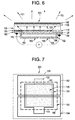
- the organic light emitting device 200 comprises an organic light emitting layer 110, a cathode 120, and an anode 130 which is light transmissive.
- the organic light emitting device 200 also includes a device substrate 125 which is light transmissive.
- the elements in Figures 6 and 7 e.g. the anode 130, cathode 120, light emitting layer 110
- the organic light emitting device 200 may optionally include a photolumincscent layer 135.
- the photoluminescent layer 135 comprises a photoluminescent material which absorbs light from the organic light emitting layer 110 and emits light typically having a longer wavelength.
- the photoluminescent material typically comprises an inorganic phosphor, but may also comprise an organic photoluminescent material such as an organic dye. Examples of phosphor materials that can be utilized include those phosphors based on cerium doped into a Y 3 Al 5 O 12 (YAG) lattice which crystallizes in the garnet structure.
- YAG Y 3 Al 5 O 12
- the YAG phosphors can be described generally as (Y 1-x- Y Gd X Ce Y ) 3 (Al 1-Z Ga Z ) 5 O 12 , wherein x + y ⁇ 1; 0 ⁇ x ⁇ 1; 0 ⁇ y ⁇ 1; and 0 ⁇ z ⁇ 1.
- the position of the peak of the emission band varies considerably in the aforementioned phosphors.
- the Ce 3+ emission can be tuned from the green ( ⁇ 540 nm; YAG:Ga,Ce) to the red ( ⁇ 600 nm; YAG:Gd:Ce) without appreciable loss in the luminescence efficiency.
- An appropriate phosphor material or blend of phosphor materials in combination with a blue or UV emission of the organic light emitting device 100 can produce a white field corresponding to a wide range of color temperatures.
- Light sources in the form of large area white light electroluminescent panels which closely approximate the color, CRI, and brightness of conventional fluorescent lamps can be made with such phosphors and organic light emitting devices.
- more than one phosphor material may be combined together and then utilized with an organic light emitting device to achieve different colors, color temperatures, and color rendition indices.
- Other phosphors which can be used are described in U.S. Serial No. 09/469,702, entitled “Luminescent Display and Method of Making", filed December 22, 1999, in the name of Anil Duggal and Alok Srivastava, which is hereby incorporated by reference.
- An example of a suitable red emitting inorganic phosphor is SrB 4 O 7 :Sm 2+ , where the Sm 2+ following the colon represents an activator. This phosphor absorbs most visible wavelengths shorter than 600 nm and emits light as a deep red line with a wavelength greater than 650 nm.
- An example of a suitable green emitting inorganic phosphor is SrGa 2 S 4 :Eu 2+ . This phosphor absorbs below 500 nm and has a maximum emission at 535 nanometers.
- An example of a suitable blue emitting inorganic phosphor is BaMg 2 Al 16 O 27 :Eu 2+ . BaMg 2 Al 16 O 27 :Eu 2+ absorbs most wavelengths below 430 nm and has a maximum emission at 450 nm.
- organic dyes which can be utilized in the photoluminescent layer include coumarin 460 (blue), coumarin 6 (green), and nile red.
- the organic light emitting device 200 may also include a scattering layer 145 comprising scattering particles such as TiO 2 or SiO 2 for effective color mixing and brightness uniformity.
- the scattering particles can also be mixed into the photoluminescent layer, rather than as a separate layer, if desired.
- a sealing member 150 Adjacent to the cathode 120 is a sealing member 150, typically comprising glass, which provides a barrier to oxygen and water.
- the sealing member 150 in conjunction with a sealant 152 which may comprise epoxy, a metal, or a glass frit, for example, provides a near hermetic barrier to prevent water and oxygen penetration into the cathode 120, anode 130 and organic light emitting layer 110.
- first and second device electrical contacts 162, 164 are Formed adjacent to the sealing member 150.
- first device electrical contact 162 connects electrically to the anode 130 in a tab region 132 of the anode 130.
- the tab region 132 is beyond the perimeter of the sealing member 150.
- the second device electrical contact 164 connects electrically to the cathode 120 in a tab region 124 of the cathode 120.
- the tab region 124 is beyond the perimeter of the sealing member 150.
- the organic light emitting layer 110 typically occupies at least the overlap region of the andoe 130 and cathode 120 and may extend beyond these electrodes.
- the device electrical contacts 162, 164 typically have respective device contacting surfaces 163, 165 which occupy a common plane. These device contacting surfaces 163, 165 facilitate the mounting of one or more organic light emitting devices 200 onto a mounting substrate, as will be described further below in connection with Figure 9.
- the imaginary surface which is typically planar, divides the organic light emitting device 200 into a first side and a second side.
- the anode 130 is on the first side
- the cathode 120 is on the second side.
- the light is emitted through the first side
- the device electrical contacts 162, 164 extend to the second side.
- the first device electrical contact 162 extends from the anode 130 on the first side to the second side of the organic light emitting device.
- the second device electrical contact 164 extends from the cathode 120 on the second side to another location on the second side of the organic light emitting device.
- the organic light emitting device 200 can be powered by contacting both device electrical contacts 162, 164 on a common planar surface 163, 165 which is on an opposite side of the organic light emitting device as where the light emission occurs.
- the planar surface defined by surfaces 163, 165 is parallel to the light emitting layer 110 and the device substrate 125. This configuration allows a number of organic light emitting devices 200 to be easily mounted adjacent to each other ("tiled") on a mounting substrate.
- the device substrate 125 can define the area of the organic light emitting device 200.
- the first and second device electrical contacts 162, 164 can occupy an area which is within the area of the device substrate 125. Therefore, two organic light emitting devices 200 can be placed directly adjacent to each other without any electrical connectors in between and with a small separation distance between the adjacent light emitting device substrates 125. For example, if desired, the separation distance could be less than 2 centimeters (cm), 1 cm, 0.5 cm or 0.25 cm, but is typically greater than 0.1 cm.
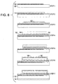
- Figure 8 illustrates a method for forming the organic light emitting device 200 of Figures 6 and 7 according to an exemplary embodiment of the invention.
- a glass substrate 125 is sputter coated with a layer of thin indium tin oxide (ITO).
- ITO is then patterned to form the anode 130, e.g in the pattern shown in Figure 7.
- the organic light emitting layer 110 (which may include one or more sublayers as shown in Figures 1-5) is deposited, for example by spin coating or inkjet processing.
- the cathode 120 is deposited as a reflective structure comprising a thin layer of lithium fluoride overcoated with aluminum, for example.
- the cathode 120 can be deposited through a stencil mask by evaporation, for example.
- the sealing member 150 which may comprise glass, for example, is next applied with a sealant 152 in step 4 to form a near hermetic barrier.
- step 5 the organic light emitting layer 110 extending beyond the sealing member 150 is removed by solvent or dry etching methods.
- the device electrical contacts 162, 164 which may comprise a metal such as aluminum or silver, are then applied to the reflective side of the organic light emitting device 200 in step 6.
- the device electrical contacts 162, 164 allow for external contact to the organic light emitting device and additionally can provide a near hermetic seal to the anode 130, cathode 120, and light emitting layer 110.
- step 7 optionally, a layer 135 of photoluminescent material, e.g. an inorganic phosphor, is applied to the device substrate 125.
- a layer 145 of scattering particles can be applied in a subsequent step.
- the steps shown in Figure 8 are of course merely an example of a method of making a light source, and not intended to be limiting.
- FIG. 9 illustrates a method of mounting one or more organic light emitting devices onto a mounting substrate to form a light source according to an exemplary embodiment of the invention.
- the term "light source” generally refers to the combination of at least one, and usually many, organic light emitting devices 200 mounted on a mounting substrate.
- Step 1 shows the mounting substrate 160, which may comprise a conventional printed circuit board such as FR4 or GETEK, or a flexible polymer film such as Kapton E TM or Kapton H TM polyimide (Kapton is a trademark of E. I.
- KaptonTM polyimide is mounted on a rigid frame (not shown in Figure 9) which rigidly supports the flexible film during processing and for end use if desired.
- An adhesive typically comprising a material capable of adhering at a low temperature, can be applied to the rigid frame.
- Suitable adhesives include materials such as ULTEM polyetherimide (ULTEMTM is a trademark of General Electric Company) and MULTIPOSITTM XP-9500 thermoset epoxy (MULTIPOSIT is a trademark of Shipley Company Inc., Marlborough, Mass.).
- step 2 another adhesive 161, which is typically organic, such as ULTEMTM, SPIE (siloxane polyimide epoxy) or other polyimide and epoxy blends, or cyanoacrylate is applied to the mounting substrate 160, as shown in Figure 9.
- step 3 one or more organic light emitting devices 200 are placed on the adhesive 161, and the adhesive is cured to bond the organic light emitting devices 200 to the mounting substrate 160.
- vias 169 are formed using laser ablation or reactive ion etching, for example, through the mounting substrate 160 and the adhesive 161 to the device contacting surfaces 163, 165 of the device electrical contacts 162, 164, respectively.
- first and second mounting electrical contacts 172, 174 are formed or inserted into the via holes 169 to make contact with the device electrical contacts 162, 164, respectively.
- the mounting electrical contacts 172, 174 can be formed as a patterned metal layer using sputter or electroless plating techniques, in combination with electroplating if desired, and patterned with a standard photoresist and etch process.
- the interconnect metallization in one embodiment comprises a thin adhesion layer of 1000 angstroms ( ⁇ ) sputtered titanium, coated by a thin layer of 3000 ⁇ sputtered copper, coated by a layer of electroplated copper to a thickness of 4 microns, for example.
- An optional buffer layer of 1000 ⁇ of titanium can be applied over the electroplated copper.
- the mounting electrical contacts 172, 174 can also be applied by the conventional methods of evaporation with a shadow mask or screen printing.
- a scattering layer 145 can be applied to organic light emitting devices 200 individually, or more typically can be applied across a number of organic light emitting devices 200, as shown in Figure 9.
- the scattering layer 145 applied across multiple organic light emitting devices 200 helps to reduce any variations in output light intensity at the gaps 175 between adjacent organic light emitting devices 200.
- a nonconductive material such as SPIE (siloxane polyimide epoxy) can be inserted into the gaps 175 between adjacent organic light emitting devices 200.
- SPIE siloxane polyimide epoxy
- embodiments of the present invention allow the organic light emitting devices 200 to be placed very close to each other on the mounting substrate 160, it may be desirable in some applications to have a larger spacing between individual organic light emitting devices 200. In such cases, it may not be desirable to have a scattering layer 145 which bridges adjacent organic light emitting devices 200.
- Spacing between organic light emitting devices 200 may also occur in the case where the mounting substrate 160 is designed to be flexible, curved, or non-planar.
- the mounting substrate 160 may be formed in any desired shape, e.g. to conform to an existing building structure.
- the organic light emitting devices 200 can be sized such that they collectively follow the shape of the mounting substrate.
- the combination of a flexible, curved, or non-planar mounting substrate and appropriately sized organic light emitting devices 200 can produce a light source having an emitting surface in many desired shapes, e.g. cylindrical, spherical, etc.
- the spacing of the organic light emitting devices 200 on the mounting substrate 160 can also be designed such that the mounting substrate 160 can form a right angle between adjacent organic light emitting devices 200. In this case, the emitting surfaces of adjacent organic light emitting devices would together form a corner with perpendicular emitting surfaces.
- an alternative sequence of attachment can be used, in which vias 169 can be formed before attachment of the individual organic light emitting devices 200.
- the vias 169 are formed through the mounting substrate 160 and the adhesive layer 161 using laser ablation, mechanical punching, mechanical drilling, or reactive ion etching, for example.
- the organic light emitting devices 200 are mounted on the mounting substrate 160.
- the mounting electrical contacts 172, 174 can then be formed in step 4 as a patterned metal layer using sputter or electroless plating techniques, which may be in combination with electroplating, evaporation with a shadow mask, or screen printing, as described above.
- a scattering layer 145 can be applied in step 5.
- This embodiment provides the advantage that the vias 169 can be drilled more easily without concern for the organic light emitting devices 200, which have not yet been installed on the mounting substrate 160 at the time of drilling.
- the organic light emitting devices 200 are mounted on the mounting substrate 160 by a conventional "flip chip" interconnect technique using an adhesive.
- the mounting substrate 160 may comprise a pre-patterned double sided flex (e.g. a Kapton polyimide) or other suitable substrate material as described above with respect to Figure 9.
- the mounting electrical contacts 172, 174 are formed in the mounting substrate 160 prior to installation of the organic light emitting devices 200.
- an adhesive 171 is applied to the organic light emitting devices 200 or to the mounting electrical contacts 172, 174.
- the adhesive 171 may comprise, for example, an anisotropically conductive adhesive, a metallic bump and non-conductive adhesive, or an isotropically conductive adhesive.
- the organic light emitting devices 200 are then mounted on the mounting substrate 160.
- a scattering layer 145 is applied. This embodiment provides the advantage that the combination of the mounting substrate 160 and mounting electrical contacts 172, 174 can be produced economically in a desired pattern, and the organic light emitting devices 200 can be mounted easily on the mounting substrate 160.
- the mounting substrate 160 is provided in the form of a roll 210.
- the mounting substrate 160 may comprise a material such as a Kapton polyimide, or other flexible material as described above with respect to Figure 9.
- the mounting substrate 160 may have a preformed adhesive layer 161 thereon.
- the mounting substrate 160 is unrolled at a desired rate and the vias 169 are formed with a drill 212, which may be a laser drill or a mechanical drill, for example. Other methods of forming the vias 169, such as mechanical punching, can be used.
- the organic light emitting devices 200 are mounted with a suitable mounting apparatus 214.
- the mounting electrical contacts 172, 174 are then formed in a subsequent step with suitable apparatus 216, by evaporation or screen printing or other method.
- FIG. 10 illustrates an example of a connection layout for six organic light emitting devices 200.
- the first mounting electrical contacts 172 are all connected to a first line 182 and the second mounting electrical contacts 174 are all connected to a second line 184.
- the plurality of organic light emitting devices 200 are activated.
- the connecting structure e.g. as shown in Figure 10, can utilize highly conductive materials such as copper to efficiently carry power to the individual organic light emitting devices 200.
Abstract
Description
- The present invention relates generally to lighting applications, and more particularly to an organic light emitting device and a light source comprising a plurality of organic light emitting devices mounted on a common substrate.
- There are many examples of lighting devices which comprise inorganic light emitting diodes (LEDs) or organic light emitting devices (OLEDs). One example is a commercially available blue-emitting inorganic gallium nitride LED which is coated with yellow-emitting phosphor particles to produce white light. The LED is essentially a point source of light rather than an extended area source of light.
- An example of an OLED is set forth in U.S. Patent 5,294,870, which describes an organic electroluminescent multicolor display device comprising an organic electroluminescent source emitting blue light with green- and red-emitting fluorescent materials applied to different subpixel areas. This device emits different colors from the different subpixel areas by color shifting with the green- and red-emitting fluorescent materials.
- Another example of an OLED is described in Junji Kido et al., "Multilayer White Light-Emitting Organic Electroluminescent Device", 267 Science 1332-1334 (1995). This device includes three emitter layers with different carrier transport properties, each emitting blue, green, or red light, which layers are used to generate white light. This OLED outputs white light over an area which is greater than that of an inorganic LED. However, its emitting area is still relatively small.
- In some lighting applications, it is desirable to have extended area light sources. Although it is theoretically possible to increase the size of known OLED devices by using larger equipment, the process of coating thin, high quality organic layers over large areas may present many technical challenges. Issues that would typically need to be addressed in scaling up production to larger sizes include, for example, uniformity of coating thickness, pinholes, particulates, CTE mismatches during thermal excursions, organic material stability to processing chemicals, and adhesion to organic and inorganic interfaces. Moreover, a defect anywhere in a large panel may necessitate scrapping the entire panel. Large equipment is also more costly.
- It would be desirable, therefore, to have a light source with a large emitting area and an effective method of making such a light source.
- The invention relates to a light source comprising a mounting substrate, at least two organic light emitting devices mounted on the mounting substrate, each of the at least two organic light emitting devices comprising a first electrode which is light transmissive, an organic light emitting layer, a second electrode, a first device electrical contact extending from the first electrode to the mounting substrate, and a second device electrical contact extending from the second electrode to the mounting substrate.
- The invention also relates to an organic light emitting device comprising a first electrode which is light transmissive, an organic light emitting layer positioned adjacent to the first electrode, the organic light emitting layer having an imaginary surface running therethrough defining a first side and a second side of the organic light emitting device, wherein the first electrode is on the first side of the organic light emitting device, a second electrode positioned adjacent to the organic light emitting layer on the second side of the organic light emitting device, a first device electrical contact extending from the first electrode to the second side of the organic light emitting device, and a second device electrical contact extending from the second electrode.
- The invention also relates to a method of making a light source comprising the steps of providing a plurality of organic light emitting devices, each of the organic light emitting devices having first and second device electrical contacts which have respective first and second device contacting surfaces which occupy a common plane, the first and second device electrical contacts being electrically connected with first and second electrodes of the organic light emitting device, respectively, and mounting the plurality of organic light emitting devices on a mounting substrate such that the first and second device contacting surfaces make electrical contact with corresponding first and second mounting electrical contacts on the mounting substrate.
- The invention will now be described in greater detail, by way of example, with reference to the drawings, in which:
- Other features and advantages of the invention will be apparent from the following detailed description of preferred embodiments and the accompanying drawings, in which:
- Figure 1 is a drawing of an organic light emitting device according to one embodiment of the invention;
- Figures 2-5 illustrate various examples of organic light emitting layers formed of two or more sublayers;
- Figure 6 is a side view of an organic light emitting device according to an exemplary embodiment of the invention;
- Figure 7 is a bottom view of the organic light emitting device of Figure 6;
- Figure 8 illustrates a method of making the organic light emitting device of Figure 6;
- Figure 9 illustrates a method of mounting a plurality of light emitting devices on a mounting substrate to produce a light source according to an exemplary embodiment of the invention;
- Figure 10 is a diagram of electrical connections to a plurality of organic light emitting devices according to an exemplary embodiment of the invention; and
- Figures 11-13 illustrate methods of mounting a plurality of light emitting devices on a mounting substrate to produce a light source according to other embodiments of the invention.
-
- Figure 1 is a drawing of an organic light emitting device according to an exemplary embodiment of the invention. The organic
light emitting device 100 includes an organiclight emitting layer 110 disposed between two electrodes, e.g., acathode 120 and ananode 130. The organiclight emitting layer 110 emits light upon application of a voltage across the anode and cathode. The organiclight emitting device 100 typically includes adevice substrate 125, such as glass or transparent plastics such as PET (MYLAR), polycarbonate, and the like, as shown in Figure 1. The term "organic light emitting device" generally refers to the combination which includes the organic light emitting layer, the cathode, and the anode, and which may also include other elements such as the device substrate, device electrical contacts, and a photoluminescent layer, as will be described below. - The anode and cathode inject charge carriers, i.e. 1 oles and electrons, into the organic
light emitting layer 110 where they recombine to form excited molecules or excitons which emit light when the molecules or excitons decay. The color of light emitted by the molecules depends on the energy difference between the excited state and the ground state of the molecules or excitons. Typically, the applied voltage is about 3-10 volts but can be up to 30 volts or more, and the external quantum efficiency (photons out/electrons in) is between 0.01% and 5%, but could be up to 10%, 20%, 30%, or more. The organiclight emitting layer 110 typically has a thickness of about 50-500 nanometers, and theelectrodes - The
cathode 120 generally comprises a material having a low work function value such that a relatively small voltage causes emission of electrons from the cathode. Thecathode 120 may comprise, for example, calcium or a metal such as gold, indium, manganese, tin, lead, aluminum, silver, magnesium, or a magnesium/silver alloy. Alternatively, the cathode can be made of two layers to enhance electron injection. Examples include a thin inner layer of LiF followed by a thicker outer layer of aluminum or silver, or a thin inner layer of calcium followed by a thicker outer layer of aluminum or silver. - The
anode 130 typically comprises a material having a high work function value. Theanode 130 is preferably transparent so that light generated in the organiclight emitting layer 110 can propagate out of the organiclight emitting device 100. Theanode 130 may comprise, for example, indium tin oxide (ITO), tin oxide, nickel, or gold. Theelectrodes - A variety of organic
light emitting layers 110 can be used in conjunction with exemplary embodiments of the invention. According to one embodiment shown in Figure 1, the organiclight emitting layer 110 comprises a single layer. The organiclight emitting layer 110 may comprise, for example, a conjugated polymer which is luminescent, a hole-transporting polymer doped with electron transport molecules and a luminescent material, or an inert polymer doped with hole transporting molecules and a luminescent material. The organiclight emitting layer 110 may also comprise an amorphous film of luminescent small organic molecules which car be doped with other luminescent molecules. - According to other embodiments of the invention shown in Figures 2-5, the organic
light emitting layer 110 comprises two or more sublayers which carry out the functions of hole injection, hole transport, electron injection, electron transport, and luminescence. Only the luminescent layer is required for a functioning device. However, the additional sublayers generally increase the efficiency with which holes and electrons recombine to produce light. Thus the organiclight emitting layer 110 can comprise 1-4 sublayers including, for example, a hole injection sublayer, a hole transport sublayer, a luminescent sublayer, and an electron injection sublayer. Also, one or more sublayers may comprise a material which achieves two or more functions such as hole injection, hole transport, electron injection, electron transport, and luminescence. - Embodiments in which the organic
light emitting layer 110 comprises a single layer, as shown in Figure 1, will now be described. - According to one embodiment, the organic
light emitting layer 110 comprises a conjugated polymer. The term conjugated polymer refers to a polymer which includes a delocalized π-electron system along the backbone of the polymer. The delocalized π-electron system provides semiconducting properties to the polymer and gives it the ability to support positive and negative charge carriers with high mobilities along the polymer chain. The polymer film has a sufficiently low concentration of extrinsic charge carriers that on applying an electric field between the electrodes, charge carriers are injected into the polymer and radiation is emitted from the polymer. Conjugated polymers are discussed, for example, in R. H. Friend, 4 Journal of Molecular Electronics 37-46 (1988). - One example of a conjugated polymer which emits light upon application of a voltage is PPV (poly(p-phenylenevinylene)). PPV emits light in the spectral range of about 500-690 nanometers and has good resistance to thermal and stress induced cracking. A suitable PPV film typically has a thickness of about 100-1000 nanometers. The PPV film can be formed by spin coating a solution of the precursor to PPV in methanol onto a substrate and heating in a vacuum oven.
- Various modifications can be made to the PPV while retaining its luminescent properties. For example, the phenylene ring of the PPV can optionally carry one or more substituents each independently selected from alkyl, alkoxy, halogen, or nitro. Other conjugated polymers derived from PPV may also be used in conjunction with exemplary embodiments of the invention. Examples of such derivatives of PPV include: 1) polymers derived by replacing the phenylene ring with a fused ring system, e.g. replacing the phenylene ring with an anthracene or napthalene ring system. These alternative ring systems may also carry one or more substituents of the type described above with respect to the phenylene ring; 2) polymers derived by replacing the phenylene ring with a heterocyclic ring system such as a furan ring. The furan ring may carry one or more substituents of the type described above in connection with the phenylene ring; 3) polymers derived by increasing the number of vinylene moieties associated with each phenylene or other ring system. The above described derivatives have different energy gaps, which allows flexibility in producing an organic
light emitting layer 110 which emits in a desired color range or ranges. Additional information on luminescent conjugated polymers is described in U.S. Patent 5,247,190. - Other examples of suitable conjugated polymers include polyfluorenes such as 2,7-substituted-9-substituted fluorenes and 9-substituted fluorene oligomers and polymers. Polyfluorenes generally have good thermal and chemical stability and high solid-state fluorescence quantum yields. The fluorenes, oligomers and polymers may be substituted at the 9-position with two hydrocarbyl moieties which may optionally contain one or more of sulfur, nitrogen, oxygen, phosphorous or silicon heteroatoms; a C5-20 ring structure formed with the 9-carbon on the fluorene ring or a C4-20 ring structure formed with the 9-carbon containing one or more heteroatoms of sulfur, nitrogen or oxygen; or a hydrocarbylidene moiety. According to one embodiment, the fluorenes are substituted at the 2- and 7-positions with aryl moieties which may further be substituted with moieties which are capable of crosslinking or chain extension or a trialkylsiloxy moiety. The fluorene polymers and oligomers may be substituted at the 2- and 7'-positions. The monomer units of the fluorene oligomers and polymers are bound to one another at the 2- and 7'-positions. The 2,7'-aryl-9-substituted fluorene oligomers and polymers may be further reacted with one another to form higher molecular weight polymers by causing the optional moieties on the
terminal 2,7'-aryl moieties, which are capable of crosslinking or chain extension, to undergo chain extension or crosslinking. - The above described fluorenes and fluorene oligomers or polymers are readily soluble in common organic solvents. They are processable into thin films or coatings by conventional techniques such as spin coating, spray coating, dip coating and roller coating. Upon curing, such films demonstrate resistance to common organic solvents and high heat resistance. Additional information on such polyfluorenes is described in U.S. Patent 5,708,130.
- Other suitable polyfluorenes which can be used in conjunction with exemplary embodiments of the invention include poly(fluorene) copolymers, such as poly(fluorene-co-anthracene)s, which exhibit blue electroluminescence. These copolymers include a polyfluorene subunit such as 2,7-dibromo-9,9-di-n-hexylfluorene (DHF) and another subunit such as 9,10-dibromoanthracene (ANT). High molecular weight copolymers from DHF and ANT can be prepared by the nickel-mediated copolymerization of the corresponding aryl dibromides. The final polymer molecular weight can be controlled by adding the end capping reagent 2-bromofluorene at different stages of the polymerization. The copolymers are thermally stable with decomposition temperatures above 400° C and are soluble in common organic solvents such as tetrahydrofuran (THF), chloroform, xylene, or chlorobenzene. They emit blue light having a wavelength of about 455 nm. Additional information on such polyfluorenes is described in Gerrit Klarner et al., "Colorfast Blue Light Emitting Random Copolymers Derived from Di-n-hexylfluorene and Anthracene", 10 Adv. Mater. 993-997 (1998).
- According to a second embodiment of a single layer device as shown in Figure 1, the organic
light emitting layer 110 comprises a molecularly doped polymer. A molecularly doped polymer typically comprises a binary solid solution of charge transporting molecules which are molecularly dispersed in an inert polymeric binder. The charge transporting molecules enhance the ability of holes and electrons to travel through the doped polymer and recombine. The inert polymer offers many alternatives in terms of available dopant materials and mechanical properties of the host polymer binder. - One example of a molecularly doped polymer comprises poly(methyl methacrylate) (PMMA) molecularly doped with the hole transporting molecule N,N'-diphenyl-N,N'-bis(3-methylsphenyl)-1,1'-biphenyl-4,4'-diamine (TPD) and the luminescent material tris(8-quinolinolato)-aluminum(III) (Alq). TDP has a high hole drift mobility of 10-3 cm2/volt-sec, while Alq is a luminescent metal complex having electron transporting properties in addition to its luminescent properties.
- The doping concentration is typically about 50%, while the molar ratio of TDP to Alq may vary from about 0.4 to 1.0, for example. A film of the doped PMMA can be prepared by mixing a dichloroethane solution containing suitable amounts of TPD, Alq, and PMMA, and dip coating the solution onto the desired substrate, e.g. an indium tin oxide (ITO) electrode. The thickness of the doped PMMA layer is typically about 100 nanometers. When activated by application of a voltage, a green emission is generated. Additional information on such doped polymers is described in Junji Kido et al., "Organic Electroluminescent Devices Based on Molecularly Doped Polymers", 61 Appl. Phys. Lett. 761-763 (1992).
- According to another embodiment of the invention shown in Figure 2, the organic
light emitting layer 110 comprises two sublayers. The first sublayer 11 provides hole transport, electron transport, and luminescent properties and is positioned adjacent thecathode 120. Thesecond sublayer 12 serves as a hole injection sublayer and is positioned adjacent theanode 130. The first sublayer 11 comprises a hole-transporting polymer doped with electron transporting molecules and a luminescent material, e.g. a dye or polymer. The hole-transporting polymer may comprise poly(N-vinylcarbazole) (PVK), for example: The electron transport molecules may comprise 2-(4-biphenyl)-5-(4-tert-butylphenyl)-1,3,4-oxadiazole (PBD), for example. The luminescent material typically comprises small molecules or polymers which act as emitting centers to vary the emission color. For example, the luminescent materials may comprise the organic dyes coumarin 460 (blue), coumarin 6 (green) or nile red. Thin films of these blends can be formed by spin coating a chloroform solution containing different amounts of PVK, electron transport molecules, and luminescent materials. For example, a suitable mixture comprises 100 weight percent PVK, 40 weight percent PBD, and 0.2-1.0 weight percent organic dye. - The
second sublayer 12 serves as a hole injection sublayer and may comprise poly(3,4)ethylenedioxythiophene/polystyrenesulphonate (PEDT/PSS), for example, available from Bayer Corporation, which can be applied by conventional methods such as spin coating. Additional information on hole-transporting polymers doped with electron transporting molecules and a luminescent material is described in Chung-Chih Wu et al., "Efficient Organic Electroluminescent Devices Using Single-Layer Doped Polymer Thin Films with Bipolar Carrier Transport Abilities", 44 IEEE Trans. on Elec. Devices 1269-1281 (1997). - According to another embodiment of the invention shown in Figure 3, the organic
light emitting layer 110 includes afirst sublayer 13 comprising a luminescent sublayer and asecond sublayer 14 comprising a hole transporting sublayer. Thehole transporting sublayer 14 may comprise an aromatic amine that is readily and reversibly oxidizable, for example. One example of such a luminescent sublayer and a hole transporting sublayer is described in A. W. Grice et al, "High Brightness and Efficiency of Blue Light-Emitting Polymer Diodes", 73 Appl. Phys. Letters 629-631 (1998), which is hereby incorporated by reference. The device described therein comprises two polymer layers sandwiched between an ITO electrode and a calcium electrode. The polymer layer next to the ITO is a hole transport layer and comprises a polymeric triphenyldiamine derivative (poly-TPD). The blue emitting polymer layer which is next to the calcium electrode is poly(9,9-dioctylfluorene). - According to another embodiment of the invention shown in Figure 4, the organic
light emitting layer 110 comprises afirst sublayer 15 which includes luminescent and hole transport properties, and asecond sublayer 16 which includes electron injection properties. Thefirst sublayer 15 comprises a polysilane, and the second sublayer comprises an oxadiazole compound. This structure produces ultraviolet (UV) light. - Polysilanes are linear silicon (Si)-backbone polymers substituted with a variety of alkyl and/or aryl side groups. In contrast to π-conjugated polymers, polysilanes are quasi one-dimensional materials with delocalized σ-conjugated electrons along the polymer backbone chain. Due to their one-dimensional direct-gap nature, polysilanes exhibit a sharp photoluminescence with a high quantum efficiency in the ultraviolet region. Examples of suitable polysilanes include poly(di-n-butylsilane) (PDBS), poly(di-n-pentylsilane) (PDPS), poly(di-n-hexylsilane) (PDHS), poly(methyl-phenylsilane) (PMPS), and poly[-bis(p-butylphenyl)silane] (PBPS). The
polysilane sublayer 15 can be applied by spin coating from a toluene solution, for example. Theelectron injection sublayer 16 may comprise 2,5-bis(4-biphenyl)-1,3,4-oxadiazole (BBD), for example. Additional information on UV-emitting polysilane organic light emitting layers is described in Hiroyuki Suzuki et al, "Near-ultraviolet Electroluminescence from Polysilanes", 331 Thin Solid Films 64-70 (1998). - According to another embodiment of the invention shown in Figure 5, the organic
light emitting layer 110 comprises ahole injecting sublayer 17, ahole transporting sublayer 18, aluminescent sublayer 19, and anelectron injecting sublayer 20. Thehole injecting sublayer 17 andhole transporting sublayer 18 efficiently provide holes to the recombination area. Theelectrode injecting sublayer 20 efficiently provides electrons to the recombination area. - The
hole injecting sublayer 17 may comprise a porphyrinic compound, such as a metal free phthalocyanine or a metal containing phthalocyanine, for example. Thehole transporting sublayer 18 may comprise a hole transporting aromatic tertiary amine, where the latter is a compound containing at least one trivalent nitrogen atom that is bonded only to carbon atoms, at least one of which is a member of an aromatic ring. Theluminescent sublayer 19 may comprise, for example, a mixed ligand aluminum chelate emitting in the blue wavelengths, such as bis(R-8-quinolinolato)-(phenolato)aluminum(III) chelate where R is a ring substituent of the 8-quinolinolato ring nucleus chosen to block the attachment of more than two 8-quinolinolato ligands to the aluminum atom. Theelectron injection sublayer 20 may comprise a metal oxinoid charge accepting compound such as a tris-chelate of aluminum. Additional information on such four-layer materials and devices are described in U.S. Patent 5,294,870. - The above examples of organic
light emitting layers 110 can be used to design an organic light emitting device which emits in one or more desired colors. For example, the organiclight emitting device 100 can emit ultraviolet, blue, green, or red light. - The following example describes a blue-emitting organic
light emitting device 100 which can be used in conjunction with exemplary embodiments of the invention. - A blue-emitting organic light emitting device was constructed as follows. Indium tin oxide (ITO) coated glass (15 ohm-square) was obtained from Applied Films Corporation and portions of it were etched away using the vapors of aqua regia. This substrate was then mechanically cleaned with a detergent, soaked in a methanol solution followed by a boiling isopropyl alcohol solution, and finally placed in an ozone cleaner for 5 minutes. An approximately 5 nanometer (nm) layer of poly(3,4)ethylenedioxythiophene/polystyrenesulphonate (PEDT/PSS) from Bayer Corporation was then spin coated onto the ITO. Approximately 100 nm of a polymer blend consisting of poly(9-vinyl carbazole) (PVK) from Aldrich Co., 2-(4-biphenylyl)-5-(4-tert-butyl-phenyl)-1,3,4-oxadiazole (PBD) from Aldrich Co., and 7-Diethylamino-4-methylcoumarin (Coumarin 460) from Exciton Co. with weight percent ratios of 100:40:1 was then spin coated onto the PEDT layer using dichloroethane as the solvent. Next, a cathode consisting of an approximately 0.8 nm layer of lithium fluoride followed by about 100 nm of aluminum was evaporated onto the device through a shadow-mask to define a cathode pattern. The device was then transferred to a glove box and a glass slide was attached to the cathode side of the device with epoxy in order to provide encapsulation. The resulting device emitted blue light upon application of a voltage.
- Referring to Figures 6 and 7, an organic light emitting device is shown according to another embodiment of the invention. The organic
light emitting device 200 comprises an organiclight emitting layer 110, acathode 120, and ananode 130 which is light transmissive. The organiclight emitting device 200 also includes adevice substrate 125 which is light transmissive. The elements in Figures 6 and 7 (e.g. theanode 130,cathode 120, light emitting layer 110) corresponding to those in Figure 1 can be formed of the same materials as described above with respect to Figure 1. Upon application of a voltage, light (represented by arrows 101) is generated in thelight emitting layer 110 and propagates through theanode 130 and thedevice substrate 125. - As shown in Figure 6, the organic
light emitting device 200 may optionally include aphotolumincscent layer 135. Thephotoluminescent layer 135 comprises a photoluminescent material which absorbs light from the organiclight emitting layer 110 and emits light typically having a longer wavelength. The photoluminescent material typically comprises an inorganic phosphor, but may also comprise an organic photoluminescent material such as an organic dye. Examples of phosphor materials that can be utilized include those phosphors based on cerium doped into a Y3Al5O12 (YAG) lattice which crystallizes in the garnet structure. Specific examples include (Y1-x-yGdxCey)3Al5O12 (YAG:Gd,Ce), (Y1-x-Cex)3Al5O12 (YAG:Ce), (Y1-xCex)3(Al1- yGay)5O12 (YAG:Ga,Ce) and (Y1-x-yGdxCey)3(Al5-zGaz)5O12 (YAG:Gd,Ga,Ce) and (Gd1- xCex)Sc2Al3O12 (GSAG). The YAG phosphors can be described generally as (Y1-x- YGdXCeY)3(Al1-ZGaZ)5O12, wherein x + y ≤ 1; 0 ≤ x ≤ 1; 0 ≤ y < 1; and 0 ≤ z ≤ 1. The position of the peak of the emission band varies considerably in the aforementioned phosphors. Depending on the garnet composition, the Ce3+ emission can be tuned from the green (∼540 nm; YAG:Ga,Ce) to the red (∼600 nm; YAG:Gd:Ce) without appreciable loss in the luminescence efficiency. An appropriate phosphor material or blend of phosphor materials in combination with a blue or UV emission of the organiclight emitting device 100 can produce a white field corresponding to a wide range of color temperatures. Light sources in the form of large area white light electroluminescent panels which closely approximate the color, CRI, and brightness of conventional fluorescent lamps can be made with such phosphors and organic light emitting devices. - In addition, more than one phosphor material may be combined together and then utilized with an organic light emitting device to achieve different colors, color temperatures, and color rendition indices. Other phosphors which can be used are described in U.S. Serial No. 09/469,702, entitled "Luminescent Display and Method of Making", filed December 22, 1999, in the name of Anil Duggal and Alok Srivastava, which is hereby incorporated by reference. An example of a suitable red emitting inorganic phosphor is SrB4O7:Sm2+, where the Sm2+ following the colon represents an activator. This phosphor absorbs most visible wavelengths shorter than 600 nm and emits light as a deep red line with a wavelength greater than 650 nm. An example of a suitable green emitting inorganic phosphor is SrGa2S4:Eu2+. This phosphor absorbs below 500 nm and has a maximum emission at 535 nanometers. An example of a suitable blue emitting inorganic phosphor is BaMg2Al16O27:Eu2+. BaMg2Al16O27:Eu2+ absorbs most wavelengths below 430 nm and has a maximum emission at 450 nm. Examples of organic dyes which can be utilized in the photoluminescent layer include coumarin 460 (blue), coumarin 6 (green), and nile red.
- Referring again to Figure 6, the organic
light emitting device 200 may also include ascattering layer 145 comprising scattering particles such as TiO2 or SiO2 for effective color mixing and brightness uniformity. The scattering particles can also be mixed into the photoluminescent layer, rather than as a separate layer, if desired. - Adjacent to the
cathode 120 is a sealingmember 150, typically comprising glass, which provides a barrier to oxygen and water. The sealingmember 150, in conjunction with asealant 152 which may comprise epoxy, a metal, or a glass frit, for example, provides a near hermetic barrier to prevent water and oxygen penetration into thecathode 120,anode 130 and organiclight emitting layer 110. - Formed adjacent to the sealing
member 150 are first and second deviceelectrical contacts anode 130 andcathode 120, respectively. As shown most clearly in-Figure 7, the first deviceelectrical contact 162 connects electrically to theanode 130 in atab region 132 of theanode 130. Thetab region 132 is beyond the perimeter of the sealingmember 150. The second deviceelectrical contact 164 connects electrically to thecathode 120 in atab region 124 of thecathode 120. Thetab region 124 is beyond the perimeter of the sealingmember 150. The organic light emitting layer 110 (not shown in Figure 7) typically occupies at least the overlap region of theandoe 130 andcathode 120 and may extend beyond these electrodes. - Referring again to Figure 6, the device
electrical contacts device contacting surfaces device contacting surfaces light emitting devices 200 onto a mounting substrate, as will be described further below in connection with Figure 9. - An advantageous feature of the device
electrical contacts light emitting layer 110. The imaginary surface, which is typically planar, divides the organiclight emitting device 200 into a first side and a second side. Theanode 130 is on the first side, and thecathode 120 is on the second side. The light is emitted through the first side, and the deviceelectrical contacts electrical contact 162 extends from theanode 130 on the first side to the second side of the organic light emitting device. The second deviceelectrical contact 164 extends from thecathode 120 on the second side to another location on the second side of the organic light emitting device. Thus, the organiclight emitting device 200 can be powered by contacting both deviceelectrical contacts planar surface surfaces light emitting layer 110 and thedevice substrate 125. This configuration allows a number of organiclight emitting devices 200 to be easily mounted adjacent to each other ("tiled") on a mounting substrate. - As shown in Figure 7, the
device substrate 125 can define the area of the organiclight emitting device 200. The first and second deviceelectrical contacts device substrate 125. Therefore, two organiclight emitting devices 200 can be placed directly adjacent to each other without any electrical connectors in between and with a small separation distance between the adjacent light emittingdevice substrates 125. For example, if desired, the separation distance could be less than 2 centimeters (cm), 1 cm, 0.5 cm or 0.25 cm, but is typically greater than 0.1 cm. - Figure 8 illustrates a method for forming the organic
light emitting device 200 of Figures 6 and 7 according to an exemplary embodiment of the invention. As shown in Figure 8,step 1, aglass substrate 125 is sputter coated with a layer of thin indium tin oxide (ITO). The ITO is then patterned to form theanode 130, e.g in the pattern shown in Figure 7. Instep 2, the organic light emitting layer 110 (which may include one or more sublayers as shown in Figures 1-5) is deposited, for example by spin coating or inkjet processing. Instep 3, thecathode 120 is deposited as a reflective structure comprising a thin layer of lithium fluoride overcoated with aluminum, for example. Thecathode 120 can be deposited through a stencil mask by evaporation, for example. The sealingmember 150, which may comprise glass, for example, is next applied with asealant 152 instep 4 to form a near hermetic barrier. - In
step 5, the organiclight emitting layer 110 extending beyond the sealingmember 150 is removed by solvent or dry etching methods. The deviceelectrical contacts light emitting device 200 instep 6. The deviceelectrical contacts anode 130,cathode 120, and light emittinglayer 110. Instep 7, optionally, alayer 135 of photoluminescent material, e.g. an inorganic phosphor, is applied to thedevice substrate 125. Optionally, alayer 145 of scattering particles can be applied in a subsequent step. The steps shown in Figure 8 are of course merely an example of a method of making a light source, and not intended to be limiting. - Figure 9 illustrates a method of mounting one or more organic light emitting devices onto a mounting substrate to form a light source according to an exemplary embodiment of the invention. The term "light source" generally refers to the combination of at least one, and usually many, organic
light emitting devices 200 mounted on a mounting substrate.Step 1 shows the mountingsubstrate 160, which may comprise a conventional printed circuit board such as FR4 or GETEK, or a flexible polymer film such as Kapton E ™ or Kapton H ™ polyimide (Kapton is a trademark of E. I. Du Pont de Nemours & Co.), Apical A V polyimide (Apical is a trademark of Kanegafugi Chemical Company), or Upilex polyimide (Upilex is a trademark of UBE Industries, Ltd) for example. In one embodiment, free-standing Kapton™ polyimide is mounted on a rigid frame (not shown in Figure 9) which rigidly supports the flexible film during processing and for end use if desired. An adhesive, typically comprising a material capable of adhering at a low temperature, can be applied to the rigid frame. Examples of suitable adhesives include materials such as ULTEM polyetherimide (ULTEM™ is a trademark of General Electric Company) and MULTIPOSIT™ XP-9500 thermoset epoxy (MULTIPOSIT is a trademark of Shipley Company Inc., Marlborough, Mass.). - In
step 2, according to one embodiment, another adhesive 161, which is typically organic, such as ULTEM™, SPIE (siloxane polyimide epoxy) or other polyimide and epoxy blends, or cyanoacrylate is applied to the mountingsubstrate 160, as shown in Figure 9. Instep 3, one or more organiclight emitting devices 200 are placed on the adhesive 161, and the adhesive is cured to bond the organiclight emitting devices 200 to the mountingsubstrate 160. - In
step 4, vias 169 are formed using laser ablation or reactive ion etching, for example, through the mountingsubstrate 160 and the adhesive 161 to thedevice contacting surfaces electrical contacts step 5, first and second mountingelectrical contacts holes 169 to make contact with the deviceelectrical contacts electrical contacts electrical contacts - In
step 6, optionally, ascattering layer 145 can be applied to organiclight emitting devices 200 individually, or more typically can be applied across a number of organiclight emitting devices 200, as shown in Figure 9. Thescattering layer 145 applied across multiple organiclight emitting devices 200 helps to reduce any variations in output light intensity at thegaps 175 between adjacent organiclight emitting devices 200. Although not shown instep 6, a nonconductive material such as SPIE (siloxane polyimide epoxy) can be inserted into thegaps 175 between adjacent organiclight emitting devices 200. Although only two organiclight emitting devices 200 are shown in Figure 9, this method can of course be used to make large area light sources comprising many individual organiclight emitting devices 200. - Although embodiments of the present invention allow the organic
light emitting devices 200 to be placed very close to each other on the mountingsubstrate 160, it may be desirable in some applications to have a larger spacing between individual organiclight emitting devices 200. In such cases, it may not be desirable to have ascattering layer 145 which bridges adjacent organiclight emitting devices 200. - Spacing between organic light emitting
devices 200 may also occur in the case where the mountingsubstrate 160 is designed to be flexible, curved, or non-planar. The mountingsubstrate 160 may be formed in any desired shape, e.g. to conform to an existing building structure. The organiclight emitting devices 200 can be sized such that they collectively follow the shape of the mounting substrate. Thus, the combination of a flexible, curved, or non-planar mounting substrate and appropriately sized organiclight emitting devices 200 can produce a light source having an emitting surface in many desired shapes, e.g. cylindrical, spherical, etc. The spacing of the organiclight emitting devices 200 on the mountingsubstrate 160 can also be designed such that the mountingsubstrate 160 can form a right angle between adjacent organiclight emitting devices 200. In this case, the emitting surfaces of adjacent organic light emitting devices would together form a corner with perpendicular emitting surfaces. - According to another embodiment of the invention shown in Figure 11, an alternative sequence of attachment can be used, in which vias 169 can be formed before attachment of the individual organic
light emitting devices 200. As shown instep 2, thevias 169 are formed through the mountingsubstrate 160 and theadhesive layer 161 using laser ablation, mechanical punching, mechanical drilling, or reactive ion etching, for example. Instep 3, the organiclight emitting devices 200 are mounted on the mountingsubstrate 160. The mountingelectrical contacts step 4 as a patterned metal layer using sputter or electroless plating techniques, which may be in combination with electroplating, evaporation with a shadow mask, or screen printing, as described above. Optionally, ascattering layer 145 can be applied instep 5. This embodiment provides the advantage that thevias 169 can be drilled more easily without concern for the organiclight emitting devices 200, which have not yet been installed on the mountingsubstrate 160 at the time of drilling. - According to a further embodiment of the invention shown in Figure 12, the organic
light emitting devices 200 are mounted on the mountingsubstrate 160 by a conventional "flip chip" interconnect technique using an adhesive. As shown in Figure 12,step 1, the mountingsubstrate 160 may comprise a pre-patterned double sided flex (e.g. a Kapton polyimide) or other suitable substrate material as described above with respect to Figure 9. The mountingelectrical contacts substrate 160 prior to installation of the organiclight emitting devices 200. Instep 2, an adhesive 171 is applied to the organiclight emitting devices 200 or to the mountingelectrical contacts light emitting devices 200 are then mounted on the mountingsubstrate 160. Optionally, instep 3, ascattering layer 145 is applied. This embodiment provides the advantage that the combination of the mountingsubstrate 160 and mountingelectrical contacts light emitting devices 200 can be mounted easily on the mountingsubstrate 160. - Another embodiment of the invention is shown in Figure 13. In this embodiment, the mounting
substrate 160 is provided in the form of aroll 210. The mountingsubstrate 160 may comprise a material such as a Kapton polyimide, or other flexible material as described above with respect to Figure 9. The mountingsubstrate 160 may have a preformedadhesive layer 161 thereon. The mountingsubstrate 160 is unrolled at a desired rate and thevias 169 are formed with adrill 212, which may be a laser drill or a mechanical drill, for example. Other methods of forming thevias 169, such as mechanical punching, can be used. Next, the organiclight emitting devices 200 are mounted with a suitable mountingapparatus 214. The mountingelectrical contacts suitable apparatus 216, by evaporation or screen printing or other method. - After the mounting electrical contacts have been installed, they can be connected to a suitable power supply. Figure 10 illustrates an example of a connection layout for six organic
light emitting devices 200. The first mountingelectrical contacts 172 are all connected to afirst line 182 and the second mountingelectrical contacts 174 are all connected to asecond line 184. Upon application of a voltage, the plurality of organiclight emitting devices 200 are activated. One advantage of exemplary embodiments of the invention is that the connecting structure, e.g. as shown in Figure 10, can utilize highly conductive materials such as copper to efficiently carry power to the individual organiclight emitting devices 200. - For the sake of good order, various features of the invention are set out in the following clauses:-
- 1. An organic light emitting device comprising:
- a first electrode which is light transmissive;
- an organic light emitting layer positioned adjacent to the first electrode, the organic light emitting layer having an imaginary surface running therethrough defining a first side and a second side of the organic light emitting device, wherein the first electrode is on the first side of the organic light emitting device;
- a second electrode positioned adjacent to the organic light emitting layer on
- the second side of the organic light emitting device;
- a first device electrical contact extending from the first electrode to the second side of the organic light emitting device; and
- a second device electrical contact extending from the second electrode.
- 2. The organic light emitting device of
clause 1, wherein the first and second device electrical contacts include first and second device contacting surfaces, respectively, which first and second device contacting surfaces occupy a common plane on the second side of the organic light emitting device. - 3. The organic light emitting device of
clause 1, further comprising a sealing member adjacent to the second electrode. - 4. The organic light emitting device of
clause 3, wherein the first and second device electrical contacts include first and second device contacting surfaces, respectively, which first and second device contacting surfaces occupy a common plane on the second side of the organic light emitting device adjacent to the sealing member. - 5. The organic light emitting device of
clause 1, further comprising a device substrate which is light transmissive adjacent to the first electrode. - 6. An organic light emitting device comprising:
- a first electrode which is light transmissive;
- an organic light emitting layer;
- a second electrode;
- a first device electrical contact extending from the first electrode; and
- a second device electrical contact extending from the second electrode; wherein the first and second device electrical contacts include first and second device contacting surfaces, respectively, which first and second device contacting surfaces occupy a common plane.
- 7. The organic light emitting device of
clause 6, wherein the organic light emitting layer has an imaginary surface running therethrough defining a first side and a second side of the organic light emitting device, the first electrode being on the first side of the organic light emitting device and the second electrode being on the second side of the organic light emitting device;
wherein the first and second device contacting surfaces occupy a common plane on the second side of the organic light emitting device. - 8. The organic light emitting device of
clause 6, further comprising a device substrate which is light transmissive adjacent to the first electrode. - 9. The organic light emitting device of clause 8, wherein the common plane is parallel to the organic light emitting layer and the device substrate.
- 10. A light source comprising:
- a mounting substrate;
- at least two organic light emitting devices mounted on the mounting substrate, each of the at least two organic light emitting devices comprising:
- a first electrode which is light transmissive;
- an organic light emitting layer;
- a second electrode;
- a first device electrical contact extending from the first electrode to the mounting substrate; and a second device electrical contact extending from the second electrode to the mounting substrate.
- 11. The light source of clause 10, wherein the first and second device electrical contacts include first and second device contacting surfaces, respectively, which first and second device contacting surfaces occupy a common plane which interfaces with the mounting substrate.
- 12. The light source of clause 10, wherein the mounting substrate includes mounting electrical contacts which interface with the first and second device electrical contacts of the organic light emitting devices.
- 13. The light source of
clause 12, wherein the mounting electrical contacts each comprise a metal coating on a via. - 14. The light source of
clause 13, wherein the metal coating has a through hole. - 15. The light source of
clause 13, wherein the metal coating does not have a through hole. - 16. The light source of clause 10, wherein, for each of the at least two organic light emitting devices, the mounting substrate is on one side of the light emitting layer and the first electrode is on an opposite side of the light emitting layer.
- 17. The light source of
clause 16, wherein each of the at least two organic light emitting devices further comprises a device substrate which is light transmissive adjacent to the first electrode. - 18. The light source of clause 10, wherein
each of the at least two organic light emitting devices further comprises a y device substrate which is light transmissive adjacent to the first electrode; each device substrate has a rectilinear emitting area. - 19. A light source comprising:
- a mounting substrate;
- at least two organic light emitting devices mounted on the mounting substrate, each of the at least two organic light emitting devices comprising:
- a device substrate which is light transmissive;
- a first electrode which is light transmissive;
- an organic light emitting layer; and
- a second electrode;
- wherein light generated in the organic light emitting layer propagates through the first electrode and the device substrate; and
- wherein the device substrate of one of the at least two organic light emitting devices is positioned on the mounting substrate directly adjacent to the device substrate of another of the at least two organic light emitting devices such that the adjacent device substrates are separated only by a gap filled with air or a nonconductive material.
- 20. The light source of
clause 19, further comprising: - a first device electrical contact extending from the first electrode to the mounting substrate; and
- a second device electrical contact extending from the second electrode to the mounting substrate; wherein
- for each of the at least two organic light emitting devices, the mounting substrate is on one side of the light emitting layer and the device substrate is on an opposite side of the light emitting layer.
- 21. The light source of
clause 19, further comprising a layer of scattering particles which spans the gap from one device substrate to an adjacent device substrate. - 22. The light source of
clause 19, wherein the device substrate defines an area of the organic light emitting device, and the electrical connectors are disposed within the area of the organic light emitting device. - 23. The light source of
clause 19, wherein the mounting substrate is as least one of flexible, curved, or non-planar. - 24. A method of making an organic light emitting device comprising the steps of:
- providing a device substrate;
- forming a first electrode on the device substrate;
- forming an organic light emitting layer on the first electrode, the organic light emitting layer having an imaginary surface running therethrough defining a first side and a second side of the organic light emitting device, wherein the first electrode is on the first side of the organic light emitting device;
- forming a second electrode on the second side of the organic light emitting device; and
- forming a first device electrical contact on the first electrode, which first device electrical contact extends from the first electrode to the second side of the organic light emitting device.
- 25. The method of clause 24, further comprising the step of forming a second device electrical contact on the second electrode, wherein the first and second device electrical contacts have first and second device contacting surfaces which occupy a common plane.
- 26. A method of making a light source comprising the steps of providing a
plurality of organic light emitting devices, each of the organic light emitting devices
having first and second device electrical contacts which have respective first and
second device contacting surfaces which occupy a common plane, the first and second
device electrical contacts being electrically connected with first and second electrodes
of the organic light emitting device, respectively; and
mounting the plurality of organic light emitting devices on a mounting substrate such that the first and second device contacting surfaces make electrical contact with corresponding first and second mounting electrical contacts on the mounting substrate. -
Claims (10)
- An organic light emitting device comprising:a first electrode which is light transmissive;an organic light emitting layer positioned adjacent to the first electrode, the organic light emitting layer having an imaginary surface running therethrough defining a first side and a second side of the organic light emitting device, wherein the first electrode is on the first side of the organic light emitting device;a second electrode positioned adjacent to the organic light emitting layer onthe second side of the organic light emitting device;a first device electrical contact extending from the first electrode to the second side of the organic light emitting device; anda second device electrical contact extending from the second electrode.
- The organic light emitting device of claim 1, wherein the first and second device electrical contacts include first and second device contacting surfaces, respectively, which first and second device contacting surfaces occupy a common plane on the second side of the organic light emitting device.
- An organic light emitting device comprising:a first electrode which is light transmissive;an organic light emitting layer;a second electrode;a first device electrical contact extending from the first electrode; anda second device electrical contact extending from the second electrode; wherein the first and second device electrical contacts include first and second device contacting surfaces, respectively, which first and second device contacting surfaces occupy a common plane.
- The organic light emitting device of claim 3, wherein the organic light emitting layer has an imaginary surface running therethrough defining a first side and a second side of the organic light emitting device, the first electrode being on the first side of the organic light emitting device and the second electrode being on the second side of the organic light emitting device;
wherein the first and second device contacting surfaces occupy a common plane on the second side of the organic light emitting device. - A light source comprising:a mounting substrate;at least two organic light emitting devices mounted on the mounting substrate, each of the at least two organic light emitting devices comprising:a first electrode which is light transmissive;an organic light emitting layer;a second electrode;a first device electrical contact extending from the first electrode to the mounting substrate; and a second device electrical contact extending from the second electrode to the mounting substrate.
- The light source of claim 5, wherein the first and second device electrical contacts include first and second device contacting surfaces, respectively, which first and second device contacting surfaces occupy a common plane which interfaces with the mounting substrate.
- A light source comprising:a mounting substrate;at least two organic light emitting devices mounted on the mounting substrate, each of the at least two organic light emitting devices comprising:a device substrate which is light transmissive;a first electrode which is light transmissive;an organic light emitting layer; anda second electrode;wherein light generated in the organic light emitting layer propagates through the first electrode and the device substrate; andwherein the device substrate of one of the at least two organic light emitting devices is positioned on the mounting substrate directly adjacent to the device substrate of another of the at least two organic light emitting devices such that the adjacent device substrates are separated only by a gap filled with air or a nonconductive material.
- The light source of claim 7, further comprising:a first device electrical contact extending from the first electrode to the mounting substrate; anda second device electrical contact extending from the second electrode to the mounting substrate; whereinfor each of the at least two organic light emitting devices, the mounting substrate is on one side of the light emitting layer and the device substrate is on an opposite side of the light emitting layer.
- A method of making an organic light emitting device comprising the steps of:providing a device substrate;forming a first electrode on the device substrate;forming an organic light emitting layer on the first electrode, the organic light emitting layer having an imaginary surface running therethrough defining a first side and a second side of the organic light emitting device, wherein the first electrode is on the first side of the organic light emitting device;forming a second electrode on the second side of the organic light emitting device; andforming a first device electrical contact on the first electrode, which first device electrical contact extends from the first electrode to the second side of the organic light emitting device.
- A method of making a light source comprising the steps of providing a plurality of organic light emitting devices, each of the organic light emitting devices having first and second device electrical contacts which have respective first and second device contacting surfaces which occupy a common plane, the first and second device electrical contacts being electrically connected with first and second electrodes of the organic light emitting device, respectively; and
mounting the plurality of organic light emitting devices on a mounting substrate such that the first and second device contacting surfaces make electrical contact with corresponding first and second mounting electrical contacts on the mounting substrate.
Applications Claiming Priority (8)
| Application Number | Priority Date | Filing Date | Title |
|---|---|---|---|
| US17845100P | 2000-01-27 | 2000-01-27 | |
| US178451P | 2000-01-27 | ||
| US19406800P | 2000-03-31 | 2000-03-31 | |
| US194068P | 2000-03-31 | ||
| US09/592,045 US6700322B1 (en) | 2000-01-27 | 2000-06-12 | Light source with organic layer and photoluminescent layer |
| US592045 | 2000-06-12 | ||
| US592078 | 2000-06-12 | ||
| US09/592,078 US6515417B1 (en) | 2000-01-27 | 2000-06-12 | Organic light emitting device and method for mounting |
Publications (3)
| Publication Number | Publication Date |
|---|---|
| EP1120838A2 true EP1120838A2 (en) | 2001-08-01 |
| EP1120838A3 EP1120838A3 (en) | 2007-01-24 |
| EP1120838B1 EP1120838B1 (en) | 2019-01-02 |
Family
ID=27497281
Family Applications (1)
| Application Number | Title | Priority Date | Filing Date |
|---|---|---|---|
| EP01300569.9A Expired - Lifetime EP1120838B1 (en) | 2000-01-27 | 2001-01-23 | Organic light emitting device and method for mounting |
Country Status (3)
| Country | Link |
|---|---|
| EP (1) | EP1120838B1 (en) |
| JP (1) | JP4993420B2 (en) |
| TW (1) | TWI273722B (en) |
Cited By (21)
| Publication number | Priority date | Publication date | Assignee | Title |
|---|---|---|---|---|
| US6565231B1 (en) | 2002-05-28 | 2003-05-20 | Eastman Kodak Company | OLED area illumination lighting apparatus |
| GB2382991A (en) * | 2001-11-17 | 2003-06-18 | Univ St Andrews | Photo-dynamic therapy device using organic semiconductor light emitters and reduced photo-pharmaceutical bleaching |
| EP1367675A1 (en) * | 2002-05-28 | 2003-12-03 | Eastman Kodak Company | OLED lighting apparatus |
| EP1367676A1 (en) * | 2002-05-28 | 2003-12-03 | Eastman Kodak Company | OLED area illumination light source having flexible substrate on a support |
| EP1403908A2 (en) * | 2002-09-30 | 2004-03-31 | Eastman Kodak Company | Oled lamp |
| EP1432050A2 (en) | 2002-12-20 | 2004-06-23 | General Electric Company | Large organic devices and methods of fabricating large organic devices |
| US6776496B2 (en) | 2002-08-19 | 2004-08-17 | Eastman Kodak Company | Area illumination lighting apparatus having OLED planar light source |
| US6787994B2 (en) | 2002-09-04 | 2004-09-07 | Eastman Kodak Company | OLED area illumination light source having a plurality of segments |
| US7011420B2 (en) | 2002-09-04 | 2006-03-14 | Eastman Kodak Company | Planar directed light source |
| EP1793261A1 (en) * | 2005-12-01 | 2007-06-06 | C.R.F. Societa Consortile per Azioni | Transparent display based on photoluminescent material |
| US7722965B2 (en) | 2003-12-26 | 2010-05-25 | Nitto Denko Corporation | Electroluminescence device, planar light source and display using the same |
| WO2011146350A1 (en) * | 2010-05-18 | 2011-11-24 | General Electric Company | Large-area flexible oled light source |
| WO2012172059A1 (en) * | 2011-06-17 | 2012-12-20 | Astron Fiamm Safety | Oled encapsulated in a full-wafer adhesive having a perforated cover |
| US8344369B2 (en) | 2001-12-28 | 2013-01-01 | Semiconductor Energy Laboratory Co., Ltd. | Vehicle that includes a display panel having a curved surface |
| US8371728B2 (en) | 2007-02-12 | 2013-02-12 | Koninklijke Philips Electronics N.V. | Control module for a lighting system, lighting system and light module for a lighting system |
| US8582058B2 (en) | 2004-06-03 | 2013-11-12 | Semiconductor Energy Laboratory Co., Ltd. | Lighting system including wiring over electrode |
| US8592852B2 (en) | 2010-05-21 | 2013-11-26 | Semiconductor Energy Laboratory Co., Ltd. | Light-emitting device and lighting device |
| US8748930B2 (en) | 2010-07-26 | 2014-06-10 | Semiconductor Energy Laboratory Co., Ltd. | Light-emitting device, lighting device, and manufacturing method of light-emitting device |
| WO2014206647A1 (en) * | 2013-06-28 | 2014-12-31 | Osram Oled Gmbh | Optoelectronic component and method for producing an optoelectronic component |
| CN105977276A (en) * | 2015-03-10 | 2016-09-28 | 三星显示有限公司 | Organic light emitting diode display |
| US10325940B2 (en) | 2001-11-30 | 2019-06-18 | Semiconductor Energy Laboratory Co., Ltd. | Vehicle, display device and manufacturing method for a semiconductor device |
Families Citing this family (8)
| Publication number | Priority date | Publication date | Assignee | Title |
|---|---|---|---|---|
| TW517356B (en) * | 2001-10-09 | 2003-01-11 | Delta Optoelectronics Inc | Package structure of display device and its packaging method |
| JP2005000914A (en) * | 2002-03-13 | 2005-01-06 | Ricoh Co Ltd | Manufacturing apparatus of functional element substrate |
| JP3838964B2 (en) | 2002-03-13 | 2006-10-25 | 株式会社リコー | Functional element substrate manufacturing equipment |
| US7541671B2 (en) * | 2005-03-31 | 2009-06-02 | General Electric Company | Organic electronic devices having external barrier layer |
| JP5336071B2 (en) * | 2007-12-21 | 2013-11-06 | ローム株式会社 | Organic light emitting device |
| JP2010186609A (en) * | 2009-02-11 | 2010-08-26 | Brother Ind Ltd | Organic el light-emitting device |
| WO2014027395A1 (en) * | 2012-08-13 | 2014-02-20 | パイオニア株式会社 | Light-emitting device equipped with organic el element |
| WO2017191800A1 (en) * | 2016-05-06 | 2017-11-09 | コニカミノルタ株式会社 | Surface light emitting device, and manufacturing method for same |
Citations (2)
| Publication number | Priority date | Publication date | Assignee | Title |
|---|---|---|---|---|
| US5302468A (en) * | 1992-01-28 | 1994-04-12 | Pioneer Electronic Corporation | Organic electroluminescent display apparatus |
| US5693170A (en) * | 1994-08-31 | 1997-12-02 | Cornell Research Foundation, Inc. | Tiled panel display assembly |
Family Cites Families (9)
| Publication number | Priority date | Publication date | Assignee | Title |
|---|---|---|---|---|
| DE19638667C2 (en) * | 1996-09-20 | 2001-05-17 | Osram Opto Semiconductors Gmbh | Mixed-color light-emitting semiconductor component with luminescence conversion element |
| JPH1092571A (en) * | 1996-09-18 | 1998-04-10 | Nec Kansai Ltd | Power supply method for electroluminescent lamp |
| JPH10162953A (en) * | 1996-12-03 | 1998-06-19 | Hokuriku Electric Ind Co Ltd | Chip type electroluminescent element |
| JPH10177894A (en) * | 1996-12-19 | 1998-06-30 | Matsushita Electric Ind Co Ltd | Distributed-electroluminescent element board |
| DE19717740C2 (en) * | 1997-04-26 | 2001-07-05 | Schoenberg & Cerny Gmbh Wien | Plastic molded body with integrated optoelectronic light field and process for its production |
| JPH10312882A (en) * | 1997-05-12 | 1998-11-24 | Matsushita Electric Ind Co Ltd | Organic electroluminescence element |
| JP3499114B2 (en) * | 1997-10-29 | 2004-02-23 | セイコープレシジョン株式会社 | EL element |
| JPH11162651A (en) * | 1997-12-01 | 1999-06-18 | Kozo Oshio | El light emitting body for decoration and el decoration unit |
| JPH11297470A (en) * | 1998-04-14 | 1999-10-29 | Matsushita Electric Ind Co Ltd | Illumination unit |
-
2001
- 2001-01-15 TW TW090100862A patent/TWI273722B/en not_active IP Right Cessation
- 2001-01-23 EP EP01300569.9A patent/EP1120838B1/en not_active Expired - Lifetime
- 2001-01-26 JP JP2001017759A patent/JP4993420B2/en not_active Expired - Lifetime
Patent Citations (2)
| Publication number | Priority date | Publication date | Assignee | Title |
|---|---|---|---|---|
| US5302468A (en) * | 1992-01-28 | 1994-04-12 | Pioneer Electronic Corporation | Organic electroluminescent display apparatus |
| US5693170A (en) * | 1994-08-31 | 1997-12-02 | Cornell Research Foundation, Inc. | Tiled panel display assembly |
Cited By (41)
| Publication number | Priority date | Publication date | Assignee | Title |
|---|---|---|---|---|
| GB2382991A (en) * | 2001-11-17 | 2003-06-18 | Univ St Andrews | Photo-dynamic therapy device using organic semiconductor light emitters and reduced photo-pharmaceutical bleaching |
| GB2382991B (en) * | 2001-11-17 | 2004-03-17 | Univ St Andrews | Therapeutic light-emitting device |
| US10325940B2 (en) | 2001-11-30 | 2019-06-18 | Semiconductor Energy Laboratory Co., Ltd. | Vehicle, display device and manufacturing method for a semiconductor device |
| US10957723B2 (en) | 2001-11-30 | 2021-03-23 | Semiconductor Energy Laboratory Co., Ltd. | Vehicle, display device and manufacturing method for a semiconductor device |
| US10629637B2 (en) | 2001-11-30 | 2020-04-21 | Semiconductor Energy Laboratory Co., Ltd. | Vehicle, display device and manufacturing method for a semiconductor device |
| US8610118B2 (en) | 2001-12-28 | 2013-12-17 | Semiconductor Energy Laboratory Co., Ltd. | Flexible display panel having curvature that matches curved surface of vehicle part |
| US9123595B2 (en) | 2001-12-28 | 2015-09-01 | Semiconductor Energy Laboratory Co., Ltd. | Method for fabricating a semiconductor device by bonding a layer to a support with curvature |
| US8344369B2 (en) | 2001-12-28 | 2013-01-01 | Semiconductor Energy Laboratory Co., Ltd. | Vehicle that includes a display panel having a curved surface |
| EP1367676A1 (en) * | 2002-05-28 | 2003-12-03 | Eastman Kodak Company | OLED area illumination light source having flexible substrate on a support |
| US6787990B2 (en) | 2002-05-28 | 2004-09-07 | Eastman Kodak Company | OLED area illumination light source having flexible substrate on a support |
| US6819036B2 (en) | 2002-05-28 | 2004-11-16 | Eastman Kodak Company | OLED lighting apparatus |
| US6565231B1 (en) | 2002-05-28 | 2003-05-20 | Eastman Kodak Company | OLED area illumination lighting apparatus |
| EP1367675A1 (en) * | 2002-05-28 | 2003-12-03 | Eastman Kodak Company | OLED lighting apparatus |
| CN100409723C (en) * | 2002-05-28 | 2008-08-06 | 伊斯曼柯达公司 | Luminous lighting device with organic light-emitting diode layer |
| EP1367674A1 (en) * | 2002-05-28 | 2003-12-03 | Eastman Kodak Company | OLED area illumination lighting apparatus |
| US6776496B2 (en) | 2002-08-19 | 2004-08-17 | Eastman Kodak Company | Area illumination lighting apparatus having OLED planar light source |
| US6787994B2 (en) | 2002-09-04 | 2004-09-07 | Eastman Kodak Company | OLED area illumination light source having a plurality of segments |
| US7011420B2 (en) | 2002-09-04 | 2006-03-14 | Eastman Kodak Company | Planar directed light source |
| US6936964B2 (en) | 2002-09-30 | 2005-08-30 | Eastman Kodak Company | OLED lamp |
| EP1403908A3 (en) * | 2002-09-30 | 2006-01-11 | Eastman Kodak Company | Oled lamp |
| EP1403908A2 (en) * | 2002-09-30 | 2004-03-31 | Eastman Kodak Company | Oled lamp |
| EP1432050A3 (en) * | 2002-12-20 | 2009-09-30 | General Electric Company | Large organic devices and methods of fabricating large organic devices |
| EP1432050A2 (en) | 2002-12-20 | 2004-06-23 | General Electric Company | Large organic devices and methods of fabricating large organic devices |
| US7722965B2 (en) | 2003-12-26 | 2010-05-25 | Nitto Denko Corporation | Electroluminescence device, planar light source and display using the same |
| US8847479B2 (en) | 2004-06-03 | 2014-09-30 | Semiconductor Energy Laboratory Co., Ltd. | Organic electroluminescent lighting system including wiring including a plurality of openings |
| US8582058B2 (en) | 2004-06-03 | 2013-11-12 | Semiconductor Energy Laboratory Co., Ltd. | Lighting system including wiring over electrode |
| US9099668B2 (en) | 2004-06-03 | 2015-08-04 | Semiconductor Energy Laboratory Co., Ltd. | Lighting system |
| EP1793261A1 (en) * | 2005-12-01 | 2007-06-06 | C.R.F. Societa Consortile per Azioni | Transparent display based on photoluminescent material |
| US8371728B2 (en) | 2007-02-12 | 2013-02-12 | Koninklijke Philips Electronics N.V. | Control module for a lighting system, lighting system and light module for a lighting system |
| WO2011146350A1 (en) * | 2010-05-18 | 2011-11-24 | General Electric Company | Large-area flexible oled light source |
| US8618731B2 (en) | 2010-05-18 | 2013-12-31 | General Electric Company | Large-area flexible OLED light source |
| CN102893395A (en) * | 2010-05-18 | 2013-01-23 | 通用电气公司 | Large-area flexible OLED light source |
| CN102893395B (en) * | 2010-05-18 | 2015-08-19 | 通用电气公司 | Large-area flexible OLED light source |
| US8592852B2 (en) | 2010-05-21 | 2013-11-26 | Semiconductor Energy Laboratory Co., Ltd. | Light-emitting device and lighting device |
| US8748930B2 (en) | 2010-07-26 | 2014-06-10 | Semiconductor Energy Laboratory Co., Ltd. | Light-emitting device, lighting device, and manufacturing method of light-emitting device |
| US9728737B2 (en) | 2010-07-26 | 2017-08-08 | Semiconductor Energy Laboratory Co., Ltd. | Light-emitting device, lighting device, and manufacturing method of light-emitting device |
| US9515293B2 (en) | 2011-06-17 | 2016-12-06 | Astron Flamm Safety Sarl | OLED encapsulated in a full-wafer adhesive having a perforated cover |
| WO2012172059A1 (en) * | 2011-06-17 | 2012-12-20 | Astron Fiamm Safety | Oled encapsulated in a full-wafer adhesive having a perforated cover |
| FR2976730A1 (en) * | 2011-06-17 | 2012-12-21 | Astron Fiamm Safety | ENCLOSURE ENCAPSULATED IN GLUE FULL PLATE WITH HOOD HOUSING |
| WO2014206647A1 (en) * | 2013-06-28 | 2014-12-31 | Osram Oled Gmbh | Optoelectronic component and method for producing an optoelectronic component |
| CN105977276A (en) * | 2015-03-10 | 2016-09-28 | 三星显示有限公司 | Organic light emitting diode display |
Also Published As
| Publication number | Publication date |
|---|---|
| JP2001257081A (en) | 2001-09-21 |
| EP1120838A3 (en) | 2007-01-24 |
| EP1120838B1 (en) | 2019-01-02 |
| JP4993420B2 (en) | 2012-08-08 |
| TWI273722B (en) | 2007-02-11 |
Similar Documents
| Publication | Publication Date | Title |
|---|---|---|
| US6515417B1 (en) | Organic light emitting device and method for mounting | |
| EP1120838B1 (en) | Organic light emitting device and method for mounting | |
| US7049757B2 (en) | Series connected OLED structure and fabrication method | |
| US7576496B2 (en) | AC powered OLED device | |
| US6841949B2 (en) | Color tunable organic electroluminescent light source | |
| US7198533B2 (en) | Method for making an OLED device | |
| US6700322B1 (en) | Light source with organic layer and photoluminescent layer | |
| US20020190661A1 (en) | AC powered oled device | |
| US6538375B1 (en) | Oled fiber light source | |
| US6847162B2 (en) | Light source with organic layer and photoluminescent layer | |
| EP1164644B1 (en) | Plastic substrates with improved barrier properties for devices sensitive to water and/or oxygen | |
| US6777871B2 (en) | Organic electroluminescent devices with enhanced light extraction | |
| EP1164817B1 (en) | Outdoor electroluminescent display devices | |
| EP1816690B1 (en) | OLED with area defined multicolor emission within a single lighting element | |
| JP2006245003A (en) | Electroluminescence device | |
| GB2392023A (en) | Series connected oled structure and fabrication method | |
| KR20100111684A (en) | Organic electroluminescence element and method for manufacturing the same |
Legal Events
| Date | Code | Title | Description |
|---|---|---|---|
| PUAI | Public reference made under article 153(3) epc to a published international application that has entered the european phase |
Free format text: ORIGINAL CODE: 0009012 |
|
| AK | Designated contracting states |
Kind code of ref document: A2 Designated state(s): AT BE CH CY DE DK ES FI FR GB GR IE IT LI LU MC NL PT SE TR |
|
| AX | Request for extension of the european patent |
Free format text: AL;LT;LV;MK;RO;SI |
|
| RIN1 | Information on inventor provided before grant (corrected) |
Inventor name: DUGGAL, ANIL RAJ Inventor name: SAIA, RICHARD JOSEPH Inventor name: TURNER, LARRY GENE Inventor name: MCCONNELEE, PAUL ALAN |
|
| PUAL | Search report despatched |
Free format text: ORIGINAL CODE: 0009013 |
|
| AK | Designated contracting states |
Kind code of ref document: A3 Designated state(s): AT BE CH CY DE DK ES FI FR GB GR IE IT LI LU MC NL PT SE TR |
|
| AX | Request for extension of the european patent |
Extension state: AL LT LV MK RO SI |
|
| 17P | Request for examination filed |
Effective date: 20070724 |
|
| AKX | Designation fees paid |
Designated state(s): DE FR GB IT |
|
| 17Q | First examination report despatched |
Effective date: 20070906 |
|
| RAP1 | Party data changed (applicant data changed or rights of an application transferred) |
Owner name: BOE TECHNOLOGY GROUP CO., LTD. |
|
| REG | Reference to a national code |
Ref country code: DE Ref legal event code: R079 Ref document number: 60151038 Country of ref document: DE Free format text: PREVIOUS MAIN CLASS: H01L0051200000 Ipc: H01L0051520000 |
|
| GRAP | Despatch of communication of intention to grant a patent |
Free format text: ORIGINAL CODE: EPIDOSNIGR1 |
|
| RIC1 | Information provided on ipc code assigned before grant |
Ipc: H01L 27/32 20060101ALI20180907BHEP Ipc: H01L 51/52 20060101AFI20180907BHEP |
|
| INTG | Intention to grant announced |
Effective date: 20181004 |
|
| RIN1 | Information on inventor provided before grant (corrected) |
Inventor name: DUGGAL, ANIL RAJ Inventor name: MCCONNELEE, PAUL ALAN Inventor name: TURNER, LARRY GENE Inventor name: SAIA, RICHARD JOSEPH |
|
| GRAS | Grant fee paid |
Free format text: ORIGINAL CODE: EPIDOSNIGR3 |
|
| GRAA | (expected) grant |
Free format text: ORIGINAL CODE: 0009210 |
|
| AK | Designated contracting states |
Kind code of ref document: B1 Designated state(s): DE FR GB IT |
|
| REG | Reference to a national code |
Ref country code: GB Ref legal event code: FG4D |
|
| REG | Reference to a national code |
Ref country code: DE Ref legal event code: R096 Ref document number: 60151038 Country of ref document: DE |
|
| REG | Reference to a national code |
Ref country code: DE Ref legal event code: R097 Ref document number: 60151038 Country of ref document: DE |
|
| PG25 | Lapsed in a contracting state [announced via postgrant information from national office to epo] |
Ref country code: IT Free format text: LAPSE BECAUSE OF FAILURE TO SUBMIT A TRANSLATION OF THE DESCRIPTION OR TO PAY THE FEE WITHIN THE PRESCRIBED TIME-LIMIT Effective date: 20190102 |
|
| PLBE | No opposition filed within time limit |
Free format text: ORIGINAL CODE: 0009261 |
|
| STAA | Information on the status of an ep patent application or granted ep patent |
Free format text: STATUS: NO OPPOSITION FILED WITHIN TIME LIMIT |
|
| 26N | No opposition filed |
Effective date: 20191003 |
|
| PGFP | Annual fee paid to national office [announced via postgrant information from national office to epo] |
Ref country code: DE Payment date: 20200121 Year of fee payment: 20 Ref country code: GB Payment date: 20200123 Year of fee payment: 20 |
|
| PGFP | Annual fee paid to national office [announced via postgrant information from national office to epo] |
Ref country code: FR Payment date: 20200121 Year of fee payment: 20 |
|
| REG | Reference to a national code |
Ref country code: DE Ref legal event code: R071 Ref document number: 60151038 Country of ref document: DE |
|
| REG | Reference to a national code |
Ref country code: GB Ref legal event code: PE20 Expiry date: 20210122 |
|
| PG25 | Lapsed in a contracting state [announced via postgrant information from national office to epo] |
Ref country code: GB Free format text: LAPSE BECAUSE OF EXPIRATION OF PROTECTION Effective date: 20210122 |