EP1122736A1 - ATD generation in a synchronous memory - Google Patents
ATD generation in a synchronous memory Download PDFInfo
- Publication number
- EP1122736A1 EP1122736A1 EP00830313A EP00830313A EP1122736A1 EP 1122736 A1 EP1122736 A1 EP 1122736A1 EP 00830313 A EP00830313 A EP 00830313A EP 00830313 A EP00830313 A EP 00830313A EP 1122736 A1 EP1122736 A1 EP 1122736A1
- Authority
- EP
- European Patent Office
- Prior art keywords
- atd
- pulse
- counter
- memory
- address
- Prior art date
- Legal status (The legal status is an assumption and is not a legal conclusion. Google has not performed a legal analysis and makes no representation as to the accuracy of the status listed.)
- Granted
Links
Images


Classifications
-
- G—PHYSICS
- G11—INFORMATION STORAGE
- G11C—STATIC STORES
- G11C7/00—Arrangements for writing information into, or reading information out from, a digital store
- G11C7/10—Input/output [I/O] data interface arrangements, e.g. I/O data control circuits, I/O data buffers
- G11C7/1051—Data output circuits, e.g. read-out amplifiers, data output buffers, data output registers, data output level conversion circuits
- G11C7/1057—Data output buffers, e.g. comprising level conversion circuits, circuits for adapting load
-
- G—PHYSICS
- G11—INFORMATION STORAGE
- G11C—STATIC STORES
- G11C7/00—Arrangements for writing information into, or reading information out from, a digital store
- G11C7/10—Input/output [I/O] data interface arrangements, e.g. I/O data control circuits, I/O data buffers
- G11C7/1015—Read-write modes for single port memories, i.e. having either a random port or a serial port
- G11C7/1018—Serial bit line access mode, e.g. using bit line address shift registers, bit line address counters, bit line burst counters
-
- G—PHYSICS
- G11—INFORMATION STORAGE
- G11C—STATIC STORES
- G11C7/00—Arrangements for writing information into, or reading information out from, a digital store
- G11C7/10—Input/output [I/O] data interface arrangements, e.g. I/O data control circuits, I/O data buffers
- G11C7/1015—Read-write modes for single port memories, i.e. having either a random port or a serial port
- G11C7/1039—Read-write modes for single port memories, i.e. having either a random port or a serial port using pipelining techniques, i.e. using latches between functional memory parts, e.g. row/column decoders, I/O buffers, sense amplifiers
-
- G—PHYSICS
- G11—INFORMATION STORAGE
- G11C—STATIC STORES
- G11C7/00—Arrangements for writing information into, or reading information out from, a digital store
- G11C7/10—Input/output [I/O] data interface arrangements, e.g. I/O data control circuits, I/O data buffers
- G11C7/1015—Read-write modes for single port memories, i.e. having either a random port or a serial port
- G11C7/1042—Read-write modes for single port memories, i.e. having either a random port or a serial port using interleaving techniques, i.e. read-write of one part of the memory while preparing another part
-
- G—PHYSICS
- G11—INFORMATION STORAGE
- G11C—STATIC STORES
- G11C7/00—Arrangements for writing information into, or reading information out from, a digital store
- G11C7/10—Input/output [I/O] data interface arrangements, e.g. I/O data control circuits, I/O data buffers
- G11C7/1015—Read-write modes for single port memories, i.e. having either a random port or a serial port
- G11C7/1045—Read-write mode select circuits
-
- G—PHYSICS
- G11—INFORMATION STORAGE
- G11C—STATIC STORES
- G11C7/00—Arrangements for writing information into, or reading information out from, a digital store
- G11C7/10—Input/output [I/O] data interface arrangements, e.g. I/O data control circuits, I/O data buffers
- G11C7/1051—Data output circuits, e.g. read-out amplifiers, data output buffers, data output registers, data output level conversion circuits
- G11C7/106—Data output latches
-
- G—PHYSICS
- G11—INFORMATION STORAGE
- G11C—STATIC STORES
- G11C7/00—Arrangements for writing information into, or reading information out from, a digital store
- G11C7/10—Input/output [I/O] data interface arrangements, e.g. I/O data control circuits, I/O data buffers
- G11C7/1051—Data output circuits, e.g. read-out amplifiers, data output buffers, data output registers, data output level conversion circuits
- G11C7/1069—I/O lines read out arrangements
-
- G—PHYSICS
- G11—INFORMATION STORAGE
- G11C—STATIC STORES
- G11C7/00—Arrangements for writing information into, or reading information out from, a digital store
- G11C7/10—Input/output [I/O] data interface arrangements, e.g. I/O data control circuits, I/O data buffers
- G11C7/1072—Input/output [I/O] data interface arrangements, e.g. I/O data control circuits, I/O data buffers for memories with random access ports synchronised on clock signal pulse trains, e.g. synchronous memories, self timed memories
-
- G—PHYSICS
- G11—INFORMATION STORAGE
- G11C—STATIC STORES
- G11C7/00—Arrangements for writing information into, or reading information out from, a digital store
- G11C7/22—Read-write [R-W] timing or clocking circuits; Read-write [R-W] control signal generators or management
-
- G—PHYSICS
- G11—INFORMATION STORAGE
- G11C—STATIC STORES
- G11C8/00—Arrangements for selecting an address in a digital store
- G11C8/04—Arrangements for selecting an address in a digital store using a sequential addressing device, e.g. shift register, counter
-
- G—PHYSICS
- G11—INFORMATION STORAGE
- G11C—STATIC STORES
- G11C8/00—Arrangements for selecting an address in a digital store
- G11C8/18—Address timing or clocking circuits; Address control signal generation or management, e.g. for row address strobe [RAS] or column address strobe [CAS] signals
Definitions
- the present invention relates in general to memory devices and in particular to interleaved memories, readable in synchronous mode by successive locations with a sequential type of access, commonly referred to as burst mode, and to standard memories read in a random access asynchronous mode with fast access times.
- the invention can be effectively used in interleaved memory devices, even if not exclusively.
- a read cycle spans from a request of data by way of the switching of the input address lines to the final extraction of the bits stored in the addressed memory location.
- the read circuitry (references, sense amplifiers, etc.) is disabled at the end of each read cycle in order to minimize energy consumption. Therefore the start of a new reading must be triggered by the generation of a suitable signal (Address Transition Detection pulse or briefly ATD) that is generally produced by a circuit sensing a change of the input address.
- a suitable signal Address Transition Detection pulse or briefly ATD
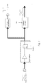
- FIG. 1 A typical ATD pulse generator is depicted in Fig. 1.
- the ATD pulse must satisfy fundamental requirements for a correct reading and for satisfying the access time requirements.
- the ATD independently from the particular architecture of the read circuitry, the ATD must be generated as quick as possible in order to quickly restart the whole analog sensing networks.
- a synchronous memory Differently from a standard memory, in a synchronous memory the addresses successive to the first one of random access (asynchronous) are internally generated by a counter incremented by a pulse coherently with the system's clock.
- a common ATD pulse generator is unsuitable because the external address lines do not switch (or are not accessible to the memory device) during synchronous read cycles.
- a different solution could be that of placing the ATD generation circuit in cascade of the counter that generates the internal addresses (during the asynchronous reading the counter works as a register, because the internal and external addresses coincide), instead of in cascade of the input address buffer, in order to generate the pulses always at the same point of the control chain, independently of the kind of access in progress.
- the present invention provides an outstanding solution to these drawbacks by using an ATD signal even for starting sequential readings, by causing its generation when the start of a new cycle of synchronous readings with sequential access is detected.
- the most appropriate signal to provide such an information is the increment pulse for the internal address counter.
- this increment pulse it is possible to generate a (pseudo) ATD signal, i.e. stimulated by an internal cause and not by the switching of the external address lines, thus starting a new reading.
- the final architecture maintains the classical structure of ATD generation, with circuits sensing the external address lines (useful for all conventional accesses) and has a block that senses the pulses of sequential increment of an internal address counter and generates the ATD pulses for starting sequential readings.
- ATD pulses a first kind due to external cause and the other kind due to internal cause can be summed by way of a logic output OR gate of the ATD generator.
- the method of the invention for synchronizing the start of sequential readings for a read cycle of a memory in burst synchronous mode consists in using the increment pulses of the address counter, or of the address counters in the case of interleaved memory devices, as synchronization signals, by generating, after each increment pulse, a dummy ATD pulse, practically undistinguishable from an ATD pulse generated by an effective switching of the input address latches.
- a ATD pulse generator conventionally sensing the external address lines is used, but modified such to include at least a pulse generator circuit stimulated by an increment pulse synchronized by a respective address counter.
- the method of the invention can advantageously contemplate the fact that the increment pulses are distinct for the counter of one or of another bank of subdivision of the array of cells of the interleaved memory, the so distinct increment pulses producing corresponding distinct dummy ATD pulses for starting sequential readings in the respective subdivision banks of the array of cells of the interleaved memory.
- An external protocol signal (ALE) or more generally an equivalent command ENABLE for enabling the input latch or latches of acquisition of externally input addresses determines, in function of its logic state, the generation of ATD pulses common to both the subdivision banks of the matrix (array) of cells of the interleaved memory, in case of read cycles in random access asynchronous mode or, according to the invention, the generation of dummy ATD pulses specifically for one or the other subdivision bank of the matrix of cells of the interleaved memory, in case of a synchronous read cycle in burst access.
- ALE external protocol signal
- the ALE signal establishes that it is necessary to start a read cycle from an external address. Being such a cycle either the first random cycle of a sequence of burst readings or a generic asynchronous access, the ATD pulse stimulated by the switching of the external address lines is sent to all the banks in the case of an interleaved memory, which will then enable their respective read structures.
- the control logic of the memory will generate a first increment pulse for the address counter of the bank (or banks) that is not in priority, for example the bank ODD, in order to generate the address on which the following (second) reading will be carried out.
- a new dummy ATD pulse is generated to start a new read cycle on the ODD bank, i.e. on the bank whose internal address is being incremented.
- a new ATD pulse dedicated to the bank EVEN will be generated to restart a new reading, while the ODD bank, having acquired priority from the control logic, will be completing the reading cycle as far as to output of the read datum.
- dedicated ATD pulses are coordinately generated to start the readings on the two banks in an alternate fashion.
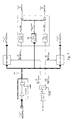
- FIG. 2 The basic diagram of the architecture of the invention for a synchronous memory is depicted in Fig. 2.
- the increment pulse of the address counter (generically indicated by the signal CONTROL in the conventional diagram of Fig. 1 ) is identified as INC_COUNTER, and in addition to the function of incrementing the counter or of the counters of the internal addresses, stimulates, by way of a suitable pulse generator circuit (PULSER), the generation of a "dummy" ATD signal, that at the output constituted by an OR logic gate, results substantially undistinguishable from the ATD pulses produced by the array of pulse generators, PULSE GENERATOR, because of a switching of the registers of external addresses.
- PULSER pulse generator circuit
- the block CONTROL LOGIC represents the logic circuit that generates the increment pulse INC_COUNTER, immediately after the detection of a rising edge of a synchronism signal of the synchronous readings, indicated as EXT_CLOCK in the diagram.
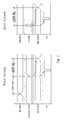
- Fig. 3 The functioning of the circuit of the invention of Fig. 2 is diagrammatically depicted in Fig. 3 in the case of a random access (RAND ACCESS) and in the case of a sequential read cycle (SYNC ACCESS).
- RAND ACCESS random access
- SYNC ACCESS sequential read cycle
- a fundamental advantage of the architecture of the invention consists in making the path of ATD be the same both in case of sequential reading and in case of random access asynchronous readings.
- the generation of the ATD pulses takes place during the same logic phase of a reading, that is when the latches that constitute the internal address counter are stabilizing themselves, whether the address is input from outside or it is internally generated through an incrementing of the counter itself.
- the same propagation delay of the ATD pulses that would be experienced during a standard random access read cycle is ensured also in case of sequential synchronous reading cycles.
- increment pulses could be used ATD pulses for readings successive to the first one, in this case it would be necessary to tie the duration of the ATD pulse, from which depends the timing of the reading and thus the access time, to the duration of the increment pulse, that on the contrary may be dictated by the particular structure and by the characteristics of the internal address counters. As a consequence, the access time would made unduly dependent from the characteristics of the address counters.
- FIG. 4 A simplified block diagram of a typical two-bank interleaved memory is depicted in Fig. 4.
- the matrix is divided into two independent banks, EVEN MATRIX and ODD MATRIX, each one of them having its own read path structure.
- the read cycles of the two banks may then superimpose to one another though out of phase.
- evaluation and transfer of the datum to the output is being carried out (OUTPUT BUFFER), on the other bank (by virtue of the fact that the location to be addressed is known) it is possible to start a new reading without waiting for the conclusion of the reading in progress on the first one.
- CONTROL tied to the external synchronization clock
- FIG. 6 An example of the timing of the main involved signals is depicted in Fig. 6 .
- Fig. 2 the basic diagram of Fig. 2 can be modified as depicted in Fig. 7.
- ATD pulse generation structure based on circuits sensing switchings of the external address lines.
- the ATD pulses generated by these circuits sensing the external address lines are common for the two banks and are used for all conventional random accesses.
- Substantially the structure of the ATD pulse generator of Fig. 7 comprises, instead of a single auxiliary pulse generator, two auxiliary pulse generators, EVEN PULSER and ODD PULSER, stimulated by specific increment signals INC_EVEN COUNTER and INC_ODD COUNTER, respectively, for the internal address counter of the EVEN bank and for the internal address counter of the ODD band which generate specific dummy ATD pulses: EVEN_ATD and ODD_ATD for the two banks for interleaved sequential readings.
- the path of the control signals (starting from the ATD pulse) in case of sequential access reading is the same of that in case of a random access reading.
- the generation of ATD pulses takes place in the same logic phase of a reading, i.e. when the latches that constitute the internal address counter are stabilizing themselves, whether the address is input from outside or it is internally generated through an incrementing of one or of the other counter.
- the same propagation delay of the ATD pulses as in the case of a standard random access read cycle is ensured and this identity of propagation delays solves in a simple and effective manner the problem of ensuring a synchronized start on the two banks of burst access readings without requiring the implementation of any further control logic.
- burst access readings take place through the same mechanisms (starting from the counters increment pulses) and using the same circuits as for random access readings, there is a further guarantee of correctness of the operation and of robustness of the architecture.
- An additional advantage is represented by the exploitation of the distinct increment pulses for the internal address counters of the two banks. In this way, no further processing is necessary for correctly conveying the dummy ATD pulse to one bank without affecting the other bank.
- the alternative of generating a common ATD pulse and successively permit propagation only toward the correct bank would require in practice a further control signal for implementing the required multiplexing (for example a priority flag signal).
Abstract
Description
- The present invention relates in general to memory devices and in particular to interleaved memories, readable in synchronous mode by successive locations with a sequential type of access, commonly referred to as burst mode, and to standard memories read in a random access asynchronous mode with fast access times. The invention can be effectively used in interleaved memory devices, even if not exclusively.
- In a standard nonvolatile memory, a read cycle spans from a request of data by way of the switching of the input address lines to the final extraction of the bits stored in the addressed memory location.
- In particular, in modern devices, the read circuitry (references, sense amplifiers, etc.) is disabled at the end of each read cycle in order to minimize energy consumption. Therefore the start of a new reading must be triggered by the generation of a suitable signal (Address Transition Detection pulse or briefly ATD) that is generally produced by a circuit sensing a change of the input address.
- A typical ATD pulse generator is depicted in Fig. 1.
- The ATD pulse must satisfy fundamental requirements for a correct reading and for satisfying the access time requirements.
- In fact, independently from the particular architecture of the read circuitry, the ATD must be generated as quick as possible in order to quickly restart the whole analog sensing networks.
- That is why it is important to generate the ATD immediately after the input buffer of the address bits. In this way, the time required for the address bits to propagate through the decoding circuitry down to select the addressed cells is simultaneously exploited to re-establish the bias conditions for an optimal reading.
- It should be noticed that the assumption from outside of a new address and the consequent generation of a new ATD before a previous access is finished, causes interruption and suppression of the previously started read cycle and the immediate start of a new read cycle, which thus superimposes to the first one, substituting it.
- In "burst" memory devices, that is operating a sequential reading, only the first reading, whose address is not predictable, must follow a standard data path. On the contrary, for successive cycles it is necessary to follow a different path.
- Differently from a standard memory, in a synchronous memory the addresses successive to the first one of random access (asynchronous) are internally generated by a counter incremented by a pulse coherently with the system's clock.
- In particular, in a synchronous memory device it is necessary to start the sequential reading, successive to the first reading, and synchronize it by internally generating the addresses, updated in a sequential manner. A common ATD pulse generator is unsuitable because the external address lines do not switch (or are not accessible to the memory device) during synchronous read cycles.
- It is also true that if a generic signal, untied from the internal addresses generation, were used for starting sequential readings, the sensing circuit would become independent from the decoding circuitry, with the risk of anticipating or delaying the start of the reading in respect to the correct selection of the memory cells to be sensed.
- In order to avoid the problem, at the start of the sequential accesses, the eventual propagation of the internally generated addresses (by introducing an appropriate delay) could be waited for. But in doing so, besides the cost in terms of silicon area requisite of such a delay chain, the control logic of the sense-amp would be greatly complicated because it will be necessary to implement two alternative data streams for the two different kinds random-asynchronous and sequential-synchronous modes of access, respectively.
- A different solution could be that of placing the ATD generation circuit in cascade of the counter that generates the internal addresses (during the asynchronous reading the counter works as a register, because the internal and external addresses coincide), instead of in cascade of the input address buffer, in order to generate the pulses always at the same point of the control chain, independently of the kind of access in progress.
- Unfortunately this solution burdens the read path in an opposite manner, because instead of starting the logic chain when a new reading has been acquired (because a change of address having been detected downstream of the input buffers), it is necessary to wait for the propagation of the signals through the latches of the counter, thus increasing the total access time.
- The present invention provides an outstanding solution to these drawbacks by using an ATD signal even for starting sequential readings, by causing its generation when the start of a new cycle of synchronous readings with sequential access is detected.
- The most appropriate signal to provide such an information is the increment pulse for the internal address counter. In fact by detecting this increment pulse it is possible to generate a (pseudo) ATD signal, i.e. stimulated by an internal cause and not by the switching of the external address lines, thus starting a new reading.
- The final architecture maintains the classical structure of ATD generation, with circuits sensing the external address lines (useful for all conventional accesses) and has a block that senses the pulses of sequential increment of an internal address counter and generates the ATD pulses for starting sequential readings.
- Finally, the two kinds of ATD pulses, a first kind due to external cause and the other kind due to internal cause can be summed by way of a logic output OR gate of the ATD generator.
- Therefore, the method of the invention for synchronizing the start of sequential readings for a read cycle of a memory in burst synchronous mode, consists in using the increment pulses of the address counter, or of the address counters in the case of interleaved memory devices, as synchronization signals, by generating, after each increment pulse, a dummy ATD pulse, practically undistinguishable from an ATD pulse generated by an effective switching of the input address latches.
- According to an aspect of the memory architecture of the invention, a ATD pulse generator conventionally sensing the external address lines is used, but modified such to include at least a pulse generator circuit stimulated by an increment pulse synchronized by a respective address counter.
- According to a preferred embodiment, in the case of an interleaved memory, the method of the invention can advantageously contemplate the fact that the increment pulses are distinct for the counter of one or of another bank of subdivision of the array of cells of the interleaved memory, the so distinct increment pulses producing corresponding distinct dummy ATD pulses for starting sequential readings in the respective subdivision banks of the array of cells of the interleaved memory.
- An external protocol signal (ALE) or more generally an equivalent command ENABLE for enabling the input latch or latches of acquisition of externally input addresses determines, in function of its logic state, the generation of ATD pulses common to both the subdivision banks of the matrix (array) of cells of the interleaved memory, in case of read cycles in random access asynchronous mode or, according to the invention, the generation of dummy ATD pulses specifically for one or the other subdivision bank of the matrix of cells of the interleaved memory, in case of a synchronous read cycle in burst access.
- The ALE signal establishes that it is necessary to start a read cycle from an external address. Being such a cycle either the first random cycle of a sequence of burst readings or a generic asynchronous access, the ATD pulse stimulated by the switching of the external address lines is sent to all the banks in the case of an interleaved memory, which will then enable their respective read structures.
- If the access were purely asynchronous, both banks will terminate the readings, but only the bank effectively addressed by the external address shall output its datum (bank priority being defined by the least significant bit A<0> of the address, as already explained).
- By contrast, because of the switching back to a low level of the signal ALE, should the read cycle be interpreted as being the first random cycle of a burst sequence, the control logic of the memory will generate a first increment pulse for the address counter of the bank (or banks) that is not in priority, for example the bank ODD, in order to generate the address on which the following (second) reading will be carried out.
- Using as a stimulation the increment pulse, destined to one or another of the internal address counters, a new dummy ATD pulse is generated to start a new read cycle on the ODD bank, i.e. on the bank whose internal address is being incremented.
- In this way, the reading on the bank EVEN is left to evolve and by way of a new dummy ATD pulse, following the generation of an internal address counter increment pulse, the reading on the other bank ODD is restarted with the updated internal address.
- At the end of a first random access cycle (that is only after having output the datum read during the first random access cycle on the EVEN bank) a new increment pulse INC_E, this time destined to the address counter of the EVEN bank on which the reading has just terminated, will be generated.
- Again, by using the address counters increment pulse, a new ATD pulse dedicated to the bank EVEN will be generated to restart a new reading, while the ODD bank, having acquired priority from the control logic, will be completing the reading cycle as far as to output of the read datum. Basically, by continuing to produce increment pulses alternately for the respective address counters, dedicated ATD pulses are coordinately generated to start the readings on the two banks in an alternate fashion.
- The different aspect and advantages of the invention will become clearer through the following description of several embodiments with reference to the attached drawings, in which:
- Figure 1 shows a classical structure for generating ATD pulses from the switching of external addresses;
- Figure 2 is a basic diagram of the architecture of the invention for generating ATD pulses for synchronous memories;
- Figure 3 illustrates graphically the ATD pulse generation processes in the case of a random access and in the case of sequential access (burst);
- Figure 4 shows a simplified block diagram of an interleaved memory;
- Figure 5 illustrates graphically the dependence between the increment pulses and the generation of internal addresses for the two banks of an interleaved memory;
- Figure 6 shows the time evolution of the main signal involved in the ATD pulse generation;
- Figure 7 is a diagram of the architecture of the invention according to an alternative embodiment that is particularly effective for interleaved memory devices.
-
- The basic diagram of the architecture of the invention for a synchronous memory is depicted in Fig. 2.
- As it can be easily noticed by comparing it to the conventional architecture of Fig. 1, in the case of the architecture of the invention, the increment pulse of the address counter (generically indicated by the signal CONTROL in the conventional diagram of Fig. 1) is identified as INC_COUNTER, and in addition to the function of incrementing the counter or of the counters of the internal addresses, stimulates, by way of a suitable pulse generator circuit (PULSER), the generation of a "dummy" ATD signal, that at the output constituted by an OR logic gate, results substantially undistinguishable from the ATD pulses produced by the array of pulse generators, PULSE GENERATOR, because of a switching of the registers of external addresses.
- The block CONTROL LOGIC represents the logic circuit that generates the increment pulse INC_COUNTER, immediately after the detection of a rising edge of a synchronism signal of the synchronous readings, indicated as EXT_CLOCK in the diagram.
- The functioning of the circuit of the invention of Fig. 2 is diagrammatically depicted in Fig. 3 in the case of a random access (RAND ACCESS) and in the case of a sequential read cycle (SYNC ACCESS).
- A fundamental advantage of the architecture of the invention consists in making the path of ATD be the same both in case of sequential reading and in case of random access asynchronous readings. In fact, the generation of the ATD pulses takes place during the same logic phase of a reading, that is when the latches that constitute the internal address counter are stabilizing themselves, whether the address is input from outside or it is internally generated through an incrementing of the counter itself. In this way, the same propagation delay of the ATD pulses that would be experienced during a standard random access read cycle is ensured also in case of sequential synchronous reading cycles.
- Fulfillment of this important condition may be easily verified by looking at the diagrams of Fig. 3.
- Although such increment pulses could be used ATD pulses for readings successive to the first one, in this case it would be necessary to tie the duration of the ATD pulse, from which depends the timing of the reading and thus the access time, to the duration of the increment pulse, that on the contrary may be dictated by the particular structure and by the characteristics of the internal address counters. As a consequence, the access time would made unduly dependent from the characteristics of the address counters.
- In interleaved memory devices only the first reading, whose address is not predictable, must follow the standard data path. On the contrary, for cycles successive to the first one, it is necessary to follow an alternative (interlaced) data path to exploit the contiguity condition, i.e. the fact that the successive cell to be read is adjacent to the one currently being read and thus its address is predictable.
- A simplified block diagram of a typical two-bank interleaved memory is depicted in Fig. 4.
- In this type of memory devices the matrix is divided into two independent banks, EVEN MATRIX and ODD MATRIX, each one of them having its own read path structure. The read cycles of the two banks may then superimpose to one another though out of phase. While on one of the two banks, evaluation and transfer of the datum to the output is being carried out (OUTPUT BUFFER), on the other bank (by virtue of the fact that the location to be addressed is known) it is possible to start a new reading without waiting for the conclusion of the reading in progress on the first one.
- By means of a control signal, CONTROL, tied to the external synchronization clock, it is possible to manage the multiplexing in the respective output MUX, alternating the priority from a bank to the other.
- Therefore, for readings successive to the first one, in order to exploit the contiguity of addresses it is necessary to generate addresses internally by means of the respective counters, EVEN COUNTER and ODD COUNTER, incremented coherently with the system's clock by the respective increment pulses INC_EVEN and INC_ODD.
- The dependence among the specific increment pulses and the generation (sequential updating) of the internal addresses of the two banks is graphically depicted in Fig. 5.
- An example of the timing of the main involved signals is depicted in Fig. 6.
- According to an alternative and particularly preferred embodiment for interleaved memory devices, the basic diagram of Fig. 2 can be modified as depicted in Fig. 7.
- It still comprises the classic ATD pulse generation structure based on circuits sensing switchings of the external address lines. The ATD pulses generated by these circuits sensing the external address lines are common for the two banks and are used for all conventional random accesses.
- Substantially the structure of the ATD pulse generator of Fig. 7 comprises, instead of a single auxiliary pulse generator, two auxiliary pulse generators, EVEN PULSER and ODD PULSER, stimulated by specific increment signals INC_EVEN COUNTER and INC_ODD COUNTER, respectively, for the internal address counter of the EVEN bank and for the internal address counter of the ODD band which generate specific dummy ATD pulses: EVEN_ATD and ODD_ATD for the two banks for interleaved sequential readings.
- During synchronous functioning, in burst mode, the generation of ATD pulses "from external addresses" is disabled by the presence of the external protocol signal ALE.
- Also in the case of an interleaved memory, the path of the control signals (starting from the ATD pulse) in case of sequential access reading is the same of that in case of a random access reading. The generation of ATD pulses takes place in the same logic phase of a reading, i.e. when the latches that constitute the internal address counter are stabilizing themselves, whether the address is input from outside or it is internally generated through an incrementing of one or of the other counter. In this way, the same propagation delay of the ATD pulses as in the case of a standard random access read cycle is ensured and this identity of propagation delays solves in a simple and effective manner the problem of ensuring a synchronized start on the two banks of burst access readings without requiring the implementation of any further control logic. Moreover, by virtue of the fact that burst access readings take place through the same mechanisms (starting from the counters increment pulses) and using the same circuits as for random access readings, there is a further guarantee of correctness of the operation and of robustness of the architecture.
- An additional advantage is represented by the exploitation of the distinct increment pulses for the internal address counters of the two banks. In this way, no further processing is necessary for correctly conveying the dummy ATD pulse to one bank without affecting the other bank. The alternative of generating a common ATD pulse and successively permit propagation only toward the correct bank would require in practice a further control signal for implementing the required multiplexing (for example a priority flag signal).
- It is thus evident that the concept of using the increment pulses to synchronize the start of sequential readings through the generation of dummy ATD pulses, undistinguishable from the ones generated by a switching of the external address lines, represents altogether an extremely efficient, easy and robust solution for synchronous memory devices and in particular for interleaved memory devices, because it allows the use of the same read control architecture and the same signal hierarchy, independently from the system used to generate the internal addresses and above all from the kind of access that is being used, whether asynchronous or sequential.
Claims (5)
- A method of synchronizing the start of sequential read cycles when reading data in a memory in a synchronous mode with sequential access, characterized in that it comprises
using the increment pulses for at least an address counter of the memory cell array as synchronization signals, by generating, following each increment pulse, a dummy ATD pulse, undistinguishable from an ATD pulse generated upon detection of a switching of external address lines. - The method according to claim 1 characterized in thatsaid memory is of an interleaved kind and said increment pulses are distinctly generated for the address counter of one and for the address counter of another bank of subdivision of the memory cell array;the distinct increment pulses generating distinct dummy ATD pulses for the start of the sequential readings in the respective banks.
- The method according to claim 1, wherein an external protocol signal (ALE) determines, in function of its own logic state, the generation of ATD pulses common to the banks of subdivision of the interleaved memory, in case of a random access to the memory by the switching of the external address lines.
- An ATD pulse generator for a memory comprising an array of buffers and respective registers functionally connected to input address pads of the memory (ATD_PAD<0,n>, ADD BUFFER, ADD LATCH), at least an address counter of the matrix of cells (ADDRESS COUNTER), an array of ATD pulse generators (PULSE GENERATORS) controlled by the outputs of said registers (ADD LATCHES) of said array for acquiring an external address and coupled to the respective inputs of a logic OR gate outputting the ATD pulse, characterized in that it comprisesa logic circuit (CONTROL LOGIC) generating increment pulses (INC_COUNTER) of said address counter (ADDRESS COUNTER) in function of an external read command (EXT_CLOCK);said increment pulse (INC_COUNTER) being input to at least a pulse generating circuit (PULSER) coupled to an input of said output OR gate.
- The generator according to claim 4, wherein said memory is an interleaved memory organized in two distinct banks (EVEN MATRIX, ODD MATRIX) each one having its own address counter (EVEN COUNTER, ODD COUNTER), said logic circuit (CONTROL LOGIC) generating distinct increment pulses (INC_EVEN COUNTER, INC_ODD COUNTER), characterized in that it comprisestwo distinct pulse generating circuits (EVEN PULSER, ODD PULSER);two distinct output logic OR gates, to the inputs of which the outputs of the registers (ADD LATCHES) of said array are functionally coupled, and to another input of which is coupled the output of a respective pulse circuit (EVEN PULSER, ODD PULSER).
Priority Applications (2)
| Application Number | Priority Date | Filing Date | Title |
|---|---|---|---|
| EP00830313A EP1122736B1 (en) | 2000-01-31 | 2000-04-27 | ATD generation in a synchronous memory |
| US09/773,760 US6625706B2 (en) | 2000-01-31 | 2001-01-31 | ATD generation in a synchronous memory |
Applications Claiming Priority (3)
| Application Number | Priority Date | Filing Date | Title |
|---|---|---|---|
| EP00830068 | 2000-01-31 | ||
| EP00830068A EP1122734B1 (en) | 2000-01-31 | 2000-01-31 | Burst interleaved memory with burst mode access in synchronous read phases wherein the two sub-arrays are independently readable with random access during asynchronous read phases |
| EP00830313A EP1122736B1 (en) | 2000-01-31 | 2000-04-27 | ATD generation in a synchronous memory |
Publications (2)
| Publication Number | Publication Date |
|---|---|
| EP1122736A1 true EP1122736A1 (en) | 2001-08-08 |
| EP1122736B1 EP1122736B1 (en) | 2009-10-28 |
Family
ID=26074118
Family Applications (1)
| Application Number | Title | Priority Date | Filing Date |
|---|---|---|---|
| EP00830313A Expired - Lifetime EP1122736B1 (en) | 2000-01-31 | 2000-04-27 | ATD generation in a synchronous memory |
Country Status (2)
| Country | Link |
|---|---|
| US (1) | US6625706B2 (en) |
| EP (1) | EP1122736B1 (en) |
Families Citing this family (3)
| Publication number | Priority date | Publication date | Assignee | Title |
|---|---|---|---|---|
| JP2004039201A (en) * | 2002-07-08 | 2004-02-05 | Nec Micro Systems Ltd | Semiconductor memory device |
| JP4494212B2 (en) * | 2002-11-12 | 2010-06-30 | メルク・シャープ・エンド・ドーム・コーポレイション | Phenylcarboxamide beta-secretase inhibitor for the treatment of Alzheimer's disease |
| US8811109B2 (en) | 2012-02-27 | 2014-08-19 | Qualcomm Incorporated | Memory pre-decoder circuits employing pulse latch(es) for reducing memory access times, and related systems and methods |
Citations (5)
| Publication number | Priority date | Publication date | Assignee | Title |
|---|---|---|---|---|
| US5488587A (en) * | 1993-10-20 | 1996-01-30 | Sharp Kabushiki Kaisha | Non-volatile dynamic random access memory |
| US5657269A (en) * | 1994-08-09 | 1997-08-12 | Yamaha Corporation | Semiconductor storage device having address-transition detecting circuit and sense-determination detecting circuit |
| US5696917A (en) * | 1994-06-03 | 1997-12-09 | Intel Corporation | Method and apparatus for performing burst read operations in an asynchronous nonvolatile memory |
| US5912860A (en) * | 1995-09-01 | 1999-06-15 | Micron Technology, Inc. | Synchronous DRAM memory with asynchronous column decode |
| US5963504A (en) * | 1994-12-23 | 1999-10-05 | Micron Technology, Inc. | Address transition detection in a synchronous design |
Family Cites Families (7)
| Publication number | Priority date | Publication date | Assignee | Title |
|---|---|---|---|---|
| US5559990A (en) | 1992-02-14 | 1996-09-24 | Advanced Micro Devices, Inc. | Memories with burst mode access |
| EP0561370B1 (en) | 1992-03-19 | 1999-06-02 | Kabushiki Kaisha Toshiba | A clock-synchronous semiconductor memory device and access method thereof |
| US5596539A (en) | 1995-12-28 | 1997-01-21 | Lsi Logic Corporation | Method and apparatus for a low power self-timed memory control system |
| US5966724A (en) | 1996-01-11 | 1999-10-12 | Micron Technology, Inc. | Synchronous memory device with dual page and burst mode operations |
| US5859623A (en) * | 1996-05-14 | 1999-01-12 | Proxima Corporation | Intelligent display system presentation projection arrangement and method of using same |
| JP4060442B2 (en) | 1998-05-28 | 2008-03-12 | 富士通株式会社 | Memory device |
| EP1122735B1 (en) * | 2000-01-31 | 2010-09-01 | STMicroelectronics Srl | Interleaved data path and output management architecture for an interleaved memory and load pulser circuit for outputting the read data |
-
2000
- 2000-04-27 EP EP00830313A patent/EP1122736B1/en not_active Expired - Lifetime
-
2001
- 2001-01-31 US US09/773,760 patent/US6625706B2/en not_active Expired - Lifetime
Patent Citations (5)
| Publication number | Priority date | Publication date | Assignee | Title |
|---|---|---|---|---|
| US5488587A (en) * | 1993-10-20 | 1996-01-30 | Sharp Kabushiki Kaisha | Non-volatile dynamic random access memory |
| US5696917A (en) * | 1994-06-03 | 1997-12-09 | Intel Corporation | Method and apparatus for performing burst read operations in an asynchronous nonvolatile memory |
| US5657269A (en) * | 1994-08-09 | 1997-08-12 | Yamaha Corporation | Semiconductor storage device having address-transition detecting circuit and sense-determination detecting circuit |
| US5963504A (en) * | 1994-12-23 | 1999-10-05 | Micron Technology, Inc. | Address transition detection in a synchronous design |
| US5912860A (en) * | 1995-09-01 | 1999-06-15 | Micron Technology, Inc. | Synchronous DRAM memory with asynchronous column decode |
Also Published As
| Publication number | Publication date |
|---|---|
| EP1122736B1 (en) | 2009-10-28 |
| US6625706B2 (en) | 2003-09-23 |
| US20010029563A1 (en) | 2001-10-11 |
Similar Documents
| Publication | Publication Date | Title |
|---|---|---|
| EP1122734B1 (en) | Burst interleaved memory with burst mode access in synchronous read phases wherein the two sub-arrays are independently readable with random access during asynchronous read phases | |
| KR950012019B1 (en) | Data output buffer of semiconductor memory device | |
| US7058799B2 (en) | Apparatus and method for clock domain crossing with integrated decode | |
| US6701419B2 (en) | Interlaced memory device with random or sequential access | |
| US6470431B2 (en) | Interleaved data path and output management architecture for an interleaved memory and load pulser circuit for outputting the read data | |
| KR100945968B1 (en) | A semiconductor memory | |
| US8773928B2 (en) | Command latency systems and methods | |
| JPS61148692A (en) | Memory device | |
| JP2000030444A (en) | Synchronizing type memory device of structure of wave pipeline | |
| JPH09106682A (en) | Control method for data output buffer of synchronous memory | |
| US7069406B2 (en) | Double data rate synchronous SRAM with 100% bus utilization | |
| US6625706B2 (en) | ATD generation in a synchronous memory | |
| US6487140B2 (en) | Circuit for managing the transfer of data streams from a plurality of sources within a system | |
| KR970051298A (en) | Semiconductor memory circuit | |
| US6356505B2 (en) | Internal regeneration of the address latch enable (ALE) signal of a protocol of management of a burst interleaved memory and related circuit | |
| EP1017059A1 (en) | Method for reading a memory, particularly a non-volatile memory | |
| US6366634B2 (en) | Accelerated carry generation | |
| US6373781B1 (en) | Priority determining circuit for non-volatile memory | |
| JPH04156629A (en) | Systme for controlling memory clock | |
| JPH0696579A (en) | Clock synchronization type semiconductor memory and accessing method therefor | |
| JPH0614435B2 (en) | Semiconductor memory | |
| JPH08335397A (en) | Semiconductor memory | |
| JPH05189294A (en) | Ram accessing system | |
| JP2002245779A (en) | Semiconductor memory | |
| JPH0935472A (en) | Synchronous semiconductor memory |
Legal Events
| Date | Code | Title | Description |
|---|---|---|---|
| PUAI | Public reference made under article 153(3) epc to a published international application that has entered the european phase |
Free format text: ORIGINAL CODE: 0009012 |
|
| AK | Designated contracting states |
Kind code of ref document: A1 Designated state(s): DE FR GB IT |
|
| AX | Request for extension of the european patent |
Free format text: AL;LT;LV;MK;RO;SI |
|
| 17P | Request for examination filed |
Effective date: 20020115 |
|
| AKX | Designation fees paid |
Free format text: DE FR GB IT |
|
| 17Q | First examination report despatched |
Effective date: 20070619 |
|
| GRAP | Despatch of communication of intention to grant a patent |
Free format text: ORIGINAL CODE: EPIDOSNIGR1 |
|
| GRAS | Grant fee paid |
Free format text: ORIGINAL CODE: EPIDOSNIGR3 |
|
| GRAA | (expected) grant |
Free format text: ORIGINAL CODE: 0009210 |
|
| AK | Designated contracting states |
Kind code of ref document: B1 Designated state(s): DE FR GB IT |
|
| REG | Reference to a national code |
Ref country code: GB Ref legal event code: FG4D |
|
| REF | Corresponds to: |
Ref document number: 60043212 Country of ref document: DE Date of ref document: 20091210 Kind code of ref document: P |
|
| RAP2 | Party data changed (patent owner data changed or rights of a patent transferred) |
Owner name: STMICROELECTRONICS SRL |
|
| PLBE | No opposition filed within time limit |
Free format text: ORIGINAL CODE: 0009261 |
|
| STAA | Information on the status of an ep patent application or granted ep patent |
Free format text: STATUS: NO OPPOSITION FILED WITHIN TIME LIMIT |
|
| 26N | No opposition filed |
Effective date: 20100729 |
|
| GBPC | Gb: european patent ceased through non-payment of renewal fee |
Effective date: 20100427 |
|
| REG | Reference to a national code |
Ref country code: FR Ref legal event code: ST Effective date: 20101230 |
|
| PG25 | Lapsed in a contracting state [announced via postgrant information from national office to epo] |
Ref country code: GB Free format text: LAPSE BECAUSE OF NON-PAYMENT OF DUE FEES Effective date: 20100427 Ref country code: IT Free format text: LAPSE BECAUSE OF FAILURE TO SUBMIT A TRANSLATION OF THE DESCRIPTION OR TO PAY THE FEE WITHIN THE PRESCRIBED TIME-LIMIT Effective date: 20091028 |
|
| PG25 | Lapsed in a contracting state [announced via postgrant information from national office to epo] |
Ref country code: FR Free format text: LAPSE BECAUSE OF NON-PAYMENT OF DUE FEES Effective date: 20100430 |
|
| PGFP | Annual fee paid to national office [announced via postgrant information from national office to epo] |
Ref country code: DE Payment date: 20190621 Year of fee payment: 20 |
|
| REG | Reference to a national code |
Ref country code: DE Ref legal event code: R071 Ref document number: 60043212 Country of ref document: DE |