EP1122850A2 - Apparatus and method for supplying and controlling electrical power - Google Patents
Apparatus and method for supplying and controlling electrical power Download PDFInfo
- Publication number
- EP1122850A2 EP1122850A2 EP01300274A EP01300274A EP1122850A2 EP 1122850 A2 EP1122850 A2 EP 1122850A2 EP 01300274 A EP01300274 A EP 01300274A EP 01300274 A EP01300274 A EP 01300274A EP 1122850 A2 EP1122850 A2 EP 1122850A2
- Authority
- EP
- European Patent Office
- Prior art keywords
- load
- primary
- power
- input
- power source
- Prior art date
- Legal status (The legal status is an assumption and is not a legal conclusion. Google has not performed a legal analysis and makes no representation as to the accuracy of the status listed.)
- Granted
Links
Images


Classifications
-
- H—ELECTRICITY
- H02—GENERATION; CONVERSION OR DISTRIBUTION OF ELECTRIC POWER
- H02J—CIRCUIT ARRANGEMENTS OR SYSTEMS FOR SUPPLYING OR DISTRIBUTING ELECTRIC POWER; SYSTEMS FOR STORING ELECTRIC ENERGY
- H02J7/00—Circuit arrangements for charging or depolarising batteries or for supplying loads from batteries
- H02J7/0063—Circuit arrangements for charging or depolarising batteries or for supplying loads from batteries with circuits adapted for supplying loads from the battery
-
- H—ELECTRICITY
- H02—GENERATION; CONVERSION OR DISTRIBUTION OF ELECTRIC POWER
- H02J—CIRCUIT ARRANGEMENTS OR SYSTEMS FOR SUPPLYING OR DISTRIBUTING ELECTRIC POWER; SYSTEMS FOR STORING ELECTRIC ENERGY
- H02J7/00—Circuit arrangements for charging or depolarising batteries or for supplying loads from batteries
- H02J7/34—Parallel operation in networks using both storage and other dc sources, e.g. providing buffering
- H02J7/345—Parallel operation in networks using both storage and other dc sources, e.g. providing buffering using capacitors as storage or buffering devices
Definitions
- the invention relates to an apparatus and method for supplying and controlling electrical power to a primary load and to a secondary load.
- Power sources used for supplying electrical power to a primary load generally have significant internal impedance, so that as the primary load increases the internal impedance has an increasingly significant effect on the output voltage of the source. Therefore, the voltage seen by a load driven by a voltage source will droop as the load draws more current because of the increase in voltage dropped across the source impedance. Where a much smaller secondary load is also driven by the power source, the voltage droop may have a disproportionate effect on the voltage range experienced at the input to the secondary load. If the same source supplies a plurality of primary loads which may draw power at independently varying times, the change in the range of voltage suppliable to the secondary load may be greater still.
- the invention provides an apparatus for supplying and controlling electrical power, comprising:
- the invention is particularly beneficial when used in association with a high power primary load, for example an electric motor driving a mechanical actuator, and a relatively low power secondary load, for example electronic control circuitry.
- a high power primary load for example an electric motor driving a mechanical actuator
- a relatively low power secondary load for example electronic control circuitry.
- the arrangement is particularly advantageous if the apparatus is in the alternative operating condition for relatively short time periods separated by relatively large time intervals because the effect of such short interruptions in power to the primary load should have little or negligible effect in practice on the performance of the primary load.
- the invention is advantageous in that the voltage seen by the secondary load when the primary load no longer draws current from the power source may approach or, in some embodiments, exceed open circuit voltage.
- the capacitor is connected to the input of a power supply device for supplying electronic circuitry.
- the range of voltage seen by the input to the power supply device can thus be reduced, thereby simplifying regulation of the power supply device.
- This facilitates the provision of a stable power supply, for example for supplying electronic circuitry, without the necessity for complex regulation arrangements which inevitably involve consequential increased manufacturing costs and/or increased weight and/or reduced reliability.
- the apparatus may be operable to change between the primary and the alternative operating conditions in response to an instant operating parameter, for example a voltage at the input to the secondary load. This facilitates more accurate control of the voltage seen by the input to the secondary load, and is also more energy efficient because the power supplied to the primary load is only interrupted when necessary.
- an instant operating parameter for example a voltage at the input to the secondary load.
- the apparatus comprises a comparator operable to repeatedly compare an operating value representing the voltage at the input to the secondary load with a predetermined reference value and to communicate to the control means the result of the comparisons for enabling the control means to temporarily change from the primary operating condition to the alternative operating condition when the voltage at the input to the secondary load falls below a minimum desired level.
- the apparatus can be arranged to control the voltage at the input to the secondary load to be above a minimum desired level.
- control means may be operable to temporarily change the operating condition of the apparatus from the primary to the alternative operating condition for predetermined time periods and/or at predetermined time intervals. This facilitates reduction of the complexity and/or weight and/or manufacturing cost of the apparatus.
- control means in the alternative operating condition of the apparatus, is operable to disconnect the primary load from the power source and provide a short circuit across the primary load. This facilitates the provision of relatively simple control circuitry.
- control means is operable to reverse the flow of current from the power source to the primary load in the alternative operating condition of the apparatus.
- This enables power from the primary load to be used to regenerate the power source during the selected time periods.
- the primary load comprises an ac motor
- collapse of flux in the motor windings when power from the source to the motor is switched off can be used to create a reverse current through the source at a higher voltage than the open circuit voltage of the source.
- a device for preventing current flowing from the secondary load input to the power source.
- This device is conveniently a diode. This enables the voltage at the input to the secondary load to be greater than the output voltage of the power source under certain operating conditions.
- the power source is preferably a d.c. power source, and may comprise a fuel cell or a battery of fuel cells.
- the control means preferably includes a d.c. to a.c. converter for supplying a primary load comprising an a.c. motor.
- the converter conveniently comprises switch means operable to switch the apparatus from the primary operating condition to the alternative operating condition.
- the switch means may comprise an electronic circuit including semiconductor switches.
- the control means preferably includes a programmable electronic control device.
- the power supply device is preferably a regulated d.c. power supply for supplying electronic control circuitry.
- the time constant of the capacitor may be of the order of tens of microseconds
- the invention also includes a method of supplying and controlling electrical power from a power source to a primary load and to a secondary load which has a capacitor connected to an input thereof, comprising temporarily interrupting the supply of power from the power source to the primary load, thereby increasing the minimum voltage the capacitor can maintain at the input to the secondary load.
- the time periods of the interruptions and/or intervals between the interruptions may be selected in response to an instant operating parameter, for example a voltage measured at the input to the secondary load.
- the time periods of the interruptions and/or intervals between the interruptions may be predetermined.
- the time periods are short compared to the time intervals.
- the time periods are conveniently in the range 10 to 20 microseconds.
- the time intervals are conveniently of the order of 2 milliseconds.
- the supply of power from the power source to the primary load may be interrupted and the load short circuited.
- the supply of power from the power source to the primary load may be interrupted and the current to the primary load reversed.
- the interruption of power to the primary load is conveniently used to cause a collapse in flux in the windings of an a.c. motor, the resulting motor generated voltage being applied to the power source and seen by the input to the secondary load.
- a motor generated voltage may be higher than the open circuit voltage of the power source. This facilitates recharging of the capacitor at a higher rate, and/or regeneration of the power source.
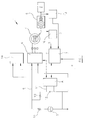
- a system 1 for controlling the movement and position of an output shaft 2 connected to an input member of an actuator (not shown).
- the system 1 includes a d.c. power source 3 for driving a primary load in the form of a three-phase motor 4 which drives the output shaft 2 via a gearbox 5.
- the power source also supplies a secondary load in the form of control means of the system 1, including a converter 6, for converting the d.c. power to a.c. for driving the motor 4, and a controller 7 for controlling the converter 6.
- the converter 6 and the controller 7 are electronic devices driven by a regulated power supply device 8. Power is supplied along a d.c. bus 9 to the converter 6 for driving the motor 4. Power for the power supply device 8 is taken from the d.c. bus 9 through a diode 10 to an input 11 of the power supply device 8.
- a capacitor 12 is connected across the terminals of the power supply device 8 to assist in temporarily maintaining the voltage at the power supply device input 11 should the voltage along the d.c. bus 9 drop.
- the desired position P of the actuator is input to the controller 7 which controls the converter 6 to drive the motor 4.
- closed loop feedback signals S, D are provided to the controller 7 respectively by a tachometer 16 connected to the motor output and by a potentiometer 13 connected to a gearbox output shaft.
- Current feedback C is also provided from the converter 6 to the controller 7.
- the system may include other channels 14 supplied by the d.c. bus 9 instead of or in addition to the converter 6, motor 4, gearbox 5, output shaft 2, and actuator channel described above. Such channels represent the primary load of the power source 3.
- the system 1 may also supply other secondary load channels such as other power supply devices, in addition to the power supply device 8.
- the d.c. power source 3 may be a fuel cell, or a battery of fuel cells. Other, alternative, suitable power sources could also be used as will readily be apparent to the skilled person.
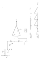
- the voltage V c provided along the d.c. bus 9 by the power source 3 will droop as shown in Figure 2c.
- the droop will be more severe the more channels that are simultaneously activated.
- the capacitor 12 is gradually discharged in satisfying the power supply requirements of device 8.
- this discharge of the capacitor produces a consequential capacitor voltage V b drop at the input 11 to the power supply device 8 as shown in Figure 2b.
- a refresh action R is initiated for a predetermined time period at regular time intervals as shown in Figure 2a and results in an increase in the d.c. bus voltage V c back to the open circuit voltage of the d.c. power source 3 for the short time periods involved.
- the capacitor 12 is refreshed during each time period to its original voltage. Since the capacitor 12 is continually refreshed, it can be used to maintain a desired minimum voltage at the input to the power supply device 8.
- the exemplary system 1 has four actuator channels, a power source open circuit voltage of 150 volts nominal, 170 volts maximum, a power source internal resistance of 0.25 ohms nominal, and a maximum current per channel of 94.5 amps (including tolerances due to measuring circuits).
- the refresh time periods have predetermined lengths of approximately 16 microseconds and the intervals between the refresh time periods have predetermined lengths of about 2 milliseconds.
- the capacitor voltage V b is maintained at or above a minimum value of 100 volts, thereby reducing the input voltage range to about 50 volts.
- the minimum d.c. bus voltage is 55.5 volts (150 volts minus (4 x 94.5 amps x 0.25 ohms) ) and the maximum d.c. bus voltage is 264.5 volts (170 volts plus (4 x 94.5 amps x 0.25 ohms) ).
- the reduction in the power supply device input voltage variation is very significant in terms of reducing the complexity of design necessary to provide effective regulation of the power supply device 8.
- the refresh action is obtained by placing the system in an alternative operating condition in which no power is drawn by the motor 4 or other primary loads.
- the system is placed in this condition for the 16 microsecond time period already described, which is very short compared to the time interval of 2 milliseconds between refresh actions.
- no current is being drawn by the primary load or loads in the alternative operating condition, there is negligible voltage drop caused by current passing through the internal resistance (source impedance) 15 of the power source 3, resulting in a rise in d.c. bus voltage V c to approximately open circuit voltage as best seen in Figure 2c.
- the time needed to refresh the power supply device capacitor 12 depends on the value of the capacitor 12 and the resistance in the charging path (dominated by the power source resistance).
- the capacitor 12 is typically chosen to be in the range 10 to 20 microFarads, and in the exemplary system is 10 microFarads. With the exemplary typical source resistance of 0.25 ohms, the refresh action can be completed in a time period of about 10 to 20 microseconds.
- the converter 6 comprises six semi-conductor switches 16a to 16f and six diodes 17a to 17f, each semiconductor switch 16a to 16f being connected in parallel with a respective one of the diodes 17a to 17f.
- Two of each of the pairs 16a, 17a to 16f, 17f are connected in series and the three sets of twinned pairs are connected in parallel across the power source.
- One end of each winding 18a, 18b and 18c of the three phase motor 4 is connected between respective ones of the twinned pairs, and the other end of each winding is connected together so that the motor is connected in star configuration.
- motors connected in a delta configuration may also be used.
- the motor is controlled by the controller 7 so as to cause the semi-conductor switches in the power electronic converter 6 to open and close sequentially. In this way pairs of motor windings are energised in a predetermined sequence.
- Such motor driving techniques are well known in the art and therefore not further discussed here.
- Figure 3 shows the motor being driven at one particular instant in time at which the controller 7 has caused semiconductor switches 16a and 16e to close so that current flows through motor windings 18a and 18b.
- the current flow path 25 is marked as a heavy line, with arrows marking the direction of current flow. In this mode, the d.c. bus voltage falls below the open-circuit voltage of the power source 3.
- each of the semiconductor switches 16d, 16e, 16f of the lower set of twinned pairs is closed, while each semiconductor switch 16a, 16b, 16c of the upper set of twinned pairs is opened.
- the closed switch 16e and the diode 17d cause a short circuit across the motor, so that the motor current 26 continues to flow through switch 16e, diode 17d and through the windings 18a, 18b as shown by the arrows in Figure 4(b).
- the controller 7 is arranged to open all of the semiconductor switches 16a to 16f. This causes the necessary refresh action by preventing current flow from the d.c. source 3.
- a reverse current 27 flows through diodes 17b and 17d to the power source as shown by the arrows in Fig 4(a), increasing the d.c. bus voltage above the voltage of power source 3, and thus recharging the capacitor 12 to a greater voltage than the maximum open circuit source voltage.
- the refresh action may be initiated in response to the instantaneous voltage sensed at the power supply device input 11.
- Figure 5 shows an exemplary arrangement for such a closed loop refresh action.
- a voltage value which is proportional to the power supply device input voltage is sensed using a voltage divider 20.
- the resultant signal is sent to a comparator 21 with hysteresis. If the sensed voltage falls below a predetermined reference voltage 22, the comparator emits a refresh signal R to the controller 7 to initiate a refresh action (Figure 5b). In this manner, the power supply device input voltage V b is maintained above a predetermined minimum voltage ( Figure 5c).
- the alternative refresh arrangement can result in an even smaller effect on overall system performance, since drive to the motor or other primary load is only interrupted if the d.c. bus voltage drops significantly, which may be an infrequent event if the system is used in a device where it is rare for all the primary loads to demand maximum power at the same time.
- the additional power losses caused by switching the semiconductor switches on and off to carry out the refresh action have negligible effect on system performance.
- the controller 7 may be a programmable device such as a microprocessor.
Abstract
Description
- The invention relates to an apparatus and method for supplying and controlling electrical power to a primary load and to a secondary load.
- Power sources used for supplying electrical power to a primary load generally have significant internal impedance, so that as the primary load increases the internal impedance has an increasingly significant effect on the output voltage of the source. Therefore, the voltage seen by a load driven by a voltage source will droop as the load draws more current because of the increase in voltage dropped across the source impedance. Where a much smaller secondary load is also driven by the power source, the voltage droop may have a disproportionate effect on the voltage range experienced at the input to the secondary load. If the same source supplies a plurality of primary loads which may draw power at independently varying times, the change in the range of voltage suppliable to the secondary load may be greater still.
- A particular problem has been experienced in the provision of a regulated power supply to provide stable current and voltage to the secondary load, as is desirable, for example, where the secondary load includes electronic circuitry. This is because regulation of such a power supply becomes more complex and expensive the wider the range of input voltage it has to cope with.
- The invention provides an apparatus for supplying and controlling electrical power, comprising:
- a power source for supplying electrical power to a primary load and a secondary load;
- a capacitor connected to an input to the secondary load; and
- control means operable to cause an operating condition of the apparatus to temporarily change from;
- a primary operating condition in which power from the power source is supplied to the primary and secondary loads to;
- an alternative operating condition in which power from the power source is not supplied to the primary load but is supplied to the secondary load;
- thereby increasing the minimum voltage the capacitor can maintain at the input to the secondary load.
-
- The invention is particularly beneficial when used in association with a high power primary load, for example an electric motor driving a mechanical actuator, and a relatively low power secondary load, for example electronic control circuitry. The arrangement is particularly advantageous if the apparatus is in the alternative operating condition for relatively short time periods separated by relatively large time intervals because the effect of such short interruptions in power to the primary load should have little or negligible effect in practice on the performance of the primary load.
- The invention is advantageous in that the voltage seen by the secondary load when the primary load no longer draws current from the power source may approach or, in some embodiments, exceed open circuit voltage.
- Preferably, the capacitor is connected to the input of a power supply device for supplying electronic circuitry.
- The range of voltage seen by the input to the power supply device can thus be reduced, thereby simplifying regulation of the power supply device. This facilitates the provision of a stable power supply, for example for supplying electronic circuitry, without the necessity for complex regulation arrangements which inevitably involve consequential increased manufacturing costs and/or increased weight and/or reduced reliability.
- The apparatus may be operable to change between the primary and the alternative operating conditions in response to an instant operating parameter, for example a voltage at the input to the secondary load. This facilitates more accurate control of the voltage seen by the input to the secondary load, and is also more energy efficient because the power supplied to the primary load is only interrupted when necessary.
- Conveniently, the apparatus comprises a comparator operable to repeatedly compare an operating value representing the voltage at the input to the secondary load with a predetermined reference value and to communicate to the control means the result of the comparisons for enabling the control means to temporarily change from the primary operating condition to the alternative operating condition when the voltage at the input to the secondary load falls below a minimum desired level. In this manner the apparatus can be arranged to control the voltage at the input to the secondary load to be above a minimum desired level.
- Alternatively, the control means may be operable to temporarily change the operating condition of the apparatus from the primary to the alternative operating condition for predetermined time periods and/or at predetermined time intervals. This facilitates reduction of the complexity and/or weight and/or manufacturing cost of the apparatus.
- Preferably, the control means, in the alternative operating condition of the apparatus, is operable to disconnect the primary load from the power source and provide a short circuit across the primary load. This facilitates the provision of relatively simple control circuitry.
- Alternatively, the control means is operable to reverse the flow of current from the power source to the primary load in the alternative operating condition of the apparatus. This enables power from the primary load to be used to regenerate the power source during the selected time periods. For example, where the primary load comprises an ac motor, collapse of flux in the motor windings when power from the source to the motor is switched off can be used to create a reverse current through the source at a higher voltage than the open circuit voltage of the source.
- Preferably, a device is provided for preventing current flowing from the secondary load input to the power source. This device is conveniently a diode. This enables the voltage at the input to the secondary load to be greater than the output voltage of the power source under certain operating conditions.
- The power source is preferably a d.c. power source, and may comprise a fuel cell or a battery of fuel cells.
- The control means preferably includes a d.c. to a.c. converter for supplying a primary load comprising an a.c. motor. The converter conveniently comprises switch means operable to switch the apparatus from the primary operating condition to the alternative operating condition. The switch means may comprise an electronic circuit including semiconductor switches.
- The control means preferably includes a programmable electronic control device.
- The power supply device is preferably a regulated d.c. power supply for supplying electronic control circuitry.
- The time constant of the capacitor may be of the order of tens of microseconds
- The invention also includes a method of supplying and controlling electrical power from a power source to a primary load and to a secondary load which has a capacitor connected to an input thereof, comprising temporarily interrupting the supply of power from the power source to the primary load, thereby increasing the minimum voltage the capacitor can maintain at the input to the secondary load.
- The time periods of the interruptions and/or intervals between the interruptions may be selected in response to an instant operating parameter, for example a voltage measured at the input to the secondary load.
- Alternatively, the time periods of the interruptions and/or intervals between the interruptions may be predetermined.
- Preferably, the time periods are short compared to the time intervals. The time periods are conveniently in the
range 10 to 20 microseconds. On the other hand, the time intervals are conveniently of the order of 2 milliseconds. - The supply of power from the power source to the primary load may be interrupted and the load short circuited. Alternatively the supply of power from the power source to the primary load may be interrupted and the current to the primary load reversed.
- Using the latter method, the interruption of power to the primary load is conveniently used to cause a collapse in flux in the windings of an a.c. motor, the resulting motor generated voltage being applied to the power source and seen by the input to the secondary load. Such a motor generated voltage may be higher than the open circuit voltage of the power source. This facilitates recharging of the capacitor at a higher rate, and/or regeneration of the power source.
- In order that the invention may be better understood, two embodiments thereof will now be described, by way of example only, with reference to the accompanying drawings, in which:
- Figure 1 is a schematic diagram showing the inter-relationship of main elements of a control system for driving and controlling a mechanical actuator;
- Figure 2 shows the variation in the voltage of a d.c. bus of the system (Figure 2c) and of a capacitor of the system (Figure 2b) with time in response to a predetermined sequence of refresh actions (Figure 2a) in accordance with a first embodiment of the invention;
- Figure 3 is a schematic diagram showing the instantaneous current flow through switch means of a converter of the system in motor-driving mode;
- Figure 4(a) is a schematic diagram showing the current flow through the converter during a refresh action in accordance with a second embodiment;
- Figure 4(b) is a schematic diagram showing the current flow through the converter during a refresh action in accordance with the first embodiment;
- Figure 5 is a schematic diagram of a portion of the system showing an arrangement including a comparator for providing alternative, closed loop, control of the refresh actions in response to the instantaneous operating voltage at the capacitor.
-
- Referring first to Figure 1, a system 1 is shown for controlling the movement and position of an output shaft 2 connected to an input member of an actuator (not shown). The system 1 includes a d.c.
power source 3 for driving a primary load in the form of a three-phase motor 4 which drives the output shaft 2 via a gearbox 5. The power source also supplies a secondary load in the form of control means of the system 1, including aconverter 6, for converting the d.c. power to a.c. for driving themotor 4, and a controller 7 for controlling theconverter 6. Theconverter 6 and the controller 7 are electronic devices driven by a regulated power supply device 8. Power is supplied along a d.c.bus 9 to theconverter 6 for driving themotor 4. Power for the power supply device 8 is taken from the d.c.bus 9 through adiode 10 to an input 11 of the power supply device 8. Acapacitor 12 is connected across the terminals of the power supply device 8 to assist in temporarily maintaining the voltage at the power supply device input 11 should the voltage along the d.c.bus 9 drop. - Current flow from the
capacitor 12 to the d.c. bus is prevented bydiode 10, enabling the voltage at the input 11 to be higher than the bus voltage under certain operating conditions. - The desired position P of the actuator is input to the controller 7 which controls the
converter 6 to drive themotor 4. In the exemplary system 1, closed loop feedback signals S, D are provided to the controller 7 respectively by atachometer 16 connected to the motor output and by apotentiometer 13 connected to a gearbox output shaft. Current feedback C is also provided from theconverter 6 to the controller 7. - The system may include
other channels 14 supplied by the d.c.bus 9 instead of or in addition to theconverter 6,motor 4, gearbox 5, output shaft 2, and actuator channel described above. Such channels represent the primary load of thepower source 3. The system 1 may also supply other secondary load channels such as other power supply devices, in addition to the power supply device 8. The d.c.power source 3 may be a fuel cell, or a battery of fuel cells. Other, alternative, suitable power sources could also be used as will readily be apparent to the skilled person. - In use, when a demand P is made to alter the position of the actuator and/or to load at least one of the primary loads, the voltage Vc provided along the d.c.
bus 9 by thepower source 3 will droop as shown in Figure 2c. Clearly, the droop will be more severe the more channels that are simultaneously activated. As the voltage Vc of the d.c.bus 9 drops, thecapacitor 12 is gradually discharged in satisfying the power supply requirements of device 8. However, this discharge of the capacitor produces a consequential capacitor voltage Vb drop at the input 11 to the power supply device 8 as shown in Figure 2b. The further the capacitor voltage Vb is allowed to drop, the greater the input voltage range with which the power supply device 8 has to cope. However, in the exemplary system, a refresh action R is initiated for a predetermined time period at regular time intervals as shown in Figure 2a and results in an increase in the d.c. bus voltage Vc back to the open circuit voltage of the d.c.power source 3 for the short time periods involved. As best seen in Figure 2b, thecapacitor 12 is refreshed during each time period to its original voltage. Since thecapacitor 12 is continually refreshed, it can be used to maintain a desired minimum voltage at the input to the power supply device 8. - It should be apparent that the refresh action reduces the range of voltage with which the power supply device 8 has to cope.
- The exemplary system 1 has four actuator channels, a power source open circuit voltage of 150 volts nominal, 170 volts maximum, a power source internal resistance of 0.25 ohms nominal, and a maximum current per channel of 94.5 amps (including tolerances due to measuring circuits). The refresh time periods have predetermined lengths of approximately 16 microseconds and the intervals between the refresh time periods have predetermined lengths of about 2 milliseconds. As shown in Figure 2b, the capacitor voltage Vb is maintained at or above a minimum value of 100 volts, thereby reducing the input voltage range to about 50 volts. These results are within the designed maximum input voltage range for the exemplary power supply device which is 80 volts to 270 volts (an operating ratio of 3.375:1). In contrast, the minimum d.c. bus voltage is 55.5 volts (150 volts minus (4 x 94.5 amps x 0.25 ohms) ) and the maximum d.c. bus voltage is 264.5 volts (170 volts plus (4 x 94.5 amps x 0.25 ohms) ). This represents a 5:1 variation in d.c. bus voltage. The reduction in the power supply device input voltage variation is very significant in terms of reducing the complexity of design necessary to provide effective regulation of the power supply device 8.
- The refresh action is obtained by placing the system in an alternative operating condition in which no power is drawn by the
motor 4 or other primary loads. The system is placed in this condition for the 16 microsecond time period already described, which is very short compared to the time interval of 2 milliseconds between refresh actions. Because no current is being drawn by the primary load or loads in the alternative operating condition, there is negligible voltage drop caused by current passing through the internal resistance (source impedance) 15 of thepower source 3, resulting in a rise in d.c. bus voltage Vc to approximately open circuit voltage as best seen in Figure 2c. Of course, the time needed to refresh the powersupply device capacitor 12 depends on the value of thecapacitor 12 and the resistance in the charging path (dominated by the power source resistance). Thecapacitor 12 is typically chosen to be in therange 10 to 20 microFarads, and in the exemplary system is 10 microFarads. With the exemplary typical source resistance of 0.25 ohms, the refresh action can be completed in a time period of about 10 to 20 microseconds. - The relatively very short time periods for which the system is in the alternative operating condition result in a 0.8% drop in the power supplied to the
motor 4 and/orother channels 14, which has negligible effect on the performance of the actuator or other driven device. - Referring now to Figures 3, 4(a) and 4(b), the
converter 6 comprises six semi-conductor switches 16a to 16f and six diodes 17a to 17f, each semiconductor switch 16a to 16f being connected in parallel with a respective one of the diodes 17a to 17f. Two of each of the pairs 16a, 17a to 16f, 17f are connected in series and the three sets of twinned pairs are connected in parallel across the power source. One end of each winding 18a, 18b and 18c of the threephase motor 4 is connected between respective ones of the twinned pairs, and the other end of each winding is connected together so that the motor is connected in star configuration. However motors connected in a delta configuration may also be used. The motor is controlled by the controller 7 so as to cause the semi-conductor switches in the powerelectronic converter 6 to open and close sequentially. In this way pairs of motor windings are energised in a predetermined sequence. Such motor driving techniques are well known in the art and therefore not further discussed here. Figure 3 shows the motor being driven at one particular instant in time at which the controller 7 has caused semiconductor switches 16a and 16e to close so that current flows throughmotor windings 18a and 18b. Thecurrent flow path 25 is marked as a heavy line, with arrows marking the direction of current flow. In this mode, the d.c. bus voltage falls below the open-circuit voltage of thepower source 3. - Referring to Figure 4(b), in the first embodiment, described with respect to Figure 2, each of the semiconductor switches 16d, 16e, 16f of the lower set of twinned pairs is closed, while each
semiconductor switch 16a, 16b, 16c of the upper set of twinned pairs is opened. This prevents supply of power from thesource 3 to themotor 4 so that the d.c. bus voltage substantially equals the open-circuit voltage of thepower source 3, thereby providing the necessary refresh action. The closed switch 16e and the diode 17d cause a short circuit across the motor, so that the motor current 26 continues to flow through switch 16e, diode 17d and through thewindings 18a, 18b as shown by the arrows in Figure 4(b). - In a second embodiment shown in Figure 4(a) the controller 7 is arranged to open all of the semiconductor switches 16a to 16f. This causes the necessary refresh action by preventing current flow from the d.c.
source 3. However, with the collapse in flux in themotor windings 18a and 18b, a reverse current 27 flows through diodes 17b and 17d to the power source as shown by the arrows in Fig 4(a), increasing the d.c. bus voltage above the voltage ofpower source 3, and thus recharging thecapacitor 12 to a greater voltage than the maximum open circuit source voltage. - Instead of the time periods and time intervals being implemented by the controller at a set time and at a constant frequency, as described above in connection with Figure 2, the refresh action may be initiated in response to the instantaneous voltage sensed at the power supply device input 11. Figure 5 shows an exemplary arrangement for such a closed loop refresh action. A voltage value which is proportional to the power supply device input voltage is sensed using a
voltage divider 20. The resultant signal is sent to acomparator 21 with hysteresis. If the sensed voltage falls below apredetermined reference voltage 22, the comparator emits a refresh signal R to the controller 7 to initiate a refresh action (Figure 5b). In this manner, the power supply device input voltage Vb is maintained above a predetermined minimum voltage (Figure 5c). The alternative refresh arrangement can result in an even smaller effect on overall system performance, since drive to the motor or other primary load is only interrupted if the d.c. bus voltage drops significantly, which may be an infrequent event if the system is used in a device where it is rare for all the primary loads to demand maximum power at the same time. The additional power losses caused by switching the semiconductor switches on and off to carry out the refresh action have negligible effect on system performance. - It will be appreciated that the invention can be used with primary loads other than the three-phase a.c. motor described and shown in the drawings, and that the skilled person will be aware of other methods of temporarily preventing the primary load from drawing power from the power source. The controller 7 may be a programmable device such as a microprocessor.
Claims (20)
- An apparatus for supplying and controlling electrical power, comprising:a power source (3) for supplying electrical power to a primary load (4) and a secondary load (6, 7, 8);a capacitor (12)connected to an input (11) to the secondary load (6, 7, 8); andcontrol means (7) operable to cause an operating condition of the apparatus to temporarily change from;a primary operating condition in which power from the power source (3) is supplied to the primary (4) and secondary (6, 7, 8) loads to;an alternative operating condition in which power from the power source (3) is not supplied to the primary load (4) but is supplied to the secondary load (6, 7, 8);thereby increasing the minimum voltage the capacitor (12) can maintain at the input (11) to the secondary load (6, 7, 8).
- An apparatus as claimed in claim 1, wherein the capacitor (12) is connected to the input (11) of a power supply device (8) for supplying electronic circuitry (6, 7).
- An apparatus as claimed in claim 1 or 2, operable to change between the primary and the alternative operating conditions in response to an instant operating parameter.
- An apparatus as claimed in claim 3, wherein the operating parameter is a voltage (Vb) at the input (11) to the secondary load (6, 7, 8).
- An apparatus as claimed in any one of the preceding claims, operable to repeatedly compare an operating value representing the voltage at the input (11) to the secondary load (6, 7, 8) with a predetermined reference value (22) and to communicate to the control means the result (R) of the comparisons for enabling the control means (7) to temporarily change from the primary operating condition to the alternative operating condition when the voltage (Vb) at the input to the secondary load falls below a minimum desired level.
- An apparatus as claimed in any one of claims 1 to 4, wherein the control means (7) is operable to temporarily change the operating condition of the apparatus from the primary to the alternative operating condition for predetermined time periods and/or at predetermined time intervals.
- An apparatus as claimed in any one of the preceding claims, wherein the control means (7), in the alternative operating condition of the apparatus, is operable to disconnect the primary load (4) from the power source (3) and provide a short circuit across the primary load (4).
- An apparatus as claimed in any one of claims 1 to 6, wherein the control means (7) is operable to reverse the flow of current from the power source (3) to the primary load (4) in the alternative operating condition of the apparatus.
- An apparatus as claimed in any one of the preceding claims, further comprising a device (10) for preventing current flowing from the secondary load input (11) to the power source (3).
- An apparatus as claimed in claim 9, wherein the device (10) is a diode.
- An apparatus as claimed in any one of the preceding claims, wherein the control means (7) includes a d.c. to a.c. converter (6) for supplying a primary load comprising an a.c. motor (4).
- An apparatus as claimed in claim 11, wherein the converter (6) comprises switch means (16a-f) operable to switch the apparatus from the primary operating condition to the alternative operating condition.
- An apparatus as claimed in any one of claims 2 to 12, wherein the power supply device (8) is a regulated d.c. power supply for supplying electronic control circuitry.
- A method of supplying and controlling electrical power from a power source (3) to a primary load (4) and to a secondary load (6, 7, 8) which has a capacitor (12) connected to an input (11) thereof, comprising temporarily interrupting the supply of power from the power source (3) to the primary load (4), thereby increasing the minimum voltage the capacitor (12) can maintain at the input (11) to the secondary load (6, 7, 8).
- A method as claimed in claim 14, wherein time periods of the interruptions and/or intervals between the interruptions are selected in response to an instant operating parameter.
- A method as claimed in claim 15, wherein the operating parameter is a voltage measured at the input (11) to the secondary load (6, 7, 8).
- A method as claimed in claim 14, wherein time periods of the interruptions and/or intervals between the interruptions are predetermined.
- A method as claimed in claim 17, wherein the time periods are short compared to the time intervals.
- A method as claimed in any one of claims 14 to 18, wherein the supply of power from the power source (3) to the primary load (4) is interrupted and the load is short circuited.
- A method as claimed in any one of claims 14 to 18, wherein the supply of power from the power source (3) to the primary load (4) is interrupted and the current to the primary load is reversed.
Applications Claiming Priority (2)
| Application Number | Priority Date | Filing Date | Title |
|---|---|---|---|
| GB0000864 | 2000-01-15 | ||
| GBGB0000864.9A GB0000864D0 (en) | 2000-01-15 | 2000-01-15 | Power supply refresh control |
Publications (3)
| Publication Number | Publication Date |
|---|---|
| EP1122850A2 true EP1122850A2 (en) | 2001-08-08 |
| EP1122850A3 EP1122850A3 (en) | 2004-01-28 |
| EP1122850B1 EP1122850B1 (en) | 2011-06-22 |
Family
ID=9883708
Family Applications (1)
| Application Number | Title | Priority Date | Filing Date |
|---|---|---|---|
| EP01300274A Expired - Lifetime EP1122850B1 (en) | 2000-01-15 | 2001-01-12 | Apparatus and method for supplying and controlling electrical power |
Country Status (3)
| Country | Link |
|---|---|
| US (1) | US6477068B2 (en) |
| EP (1) | EP1122850B1 (en) |
| GB (1) | GB0000864D0 (en) |
Families Citing this family (1)
| Publication number | Priority date | Publication date | Assignee | Title |
|---|---|---|---|---|
| US20100068566A1 (en) * | 2006-12-21 | 2010-03-18 | Sathya Motupally | Method for minimizing membrane electrode degradation in a fuel cell power plant |
Citations (5)
| Publication number | Priority date | Publication date | Assignee | Title |
|---|---|---|---|---|
| GB2263593A (en) * | 1992-01-27 | 1993-07-28 | Samsung Electronics Co Ltd | Function control of battery-operated system; mobile alarm system |
| GB2281458A (en) * | 1993-08-27 | 1995-03-01 | Nokia Telecommunications Oy | Apparatus for managing power supply to a telecommunications base station |
| US5696695A (en) * | 1995-01-05 | 1997-12-09 | Tecom Inc. | System for rate-related control of electrical loads |
| WO1998004030A1 (en) * | 1996-07-17 | 1998-01-29 | Luepges Peter | Energy loss-reduction system |
| US5761084A (en) * | 1996-07-31 | 1998-06-02 | Bay Networks, Inc. | Highly programmable backup power scheme |
Family Cites Families (8)
| Publication number | Priority date | Publication date | Assignee | Title |
|---|---|---|---|---|
| US4151387A (en) * | 1971-04-06 | 1979-04-24 | Environment/One Corporation | Metal base cookware induction heating apparatus having improved power control circuit for insuring safe operation |
| JPS5840918B2 (en) * | 1979-08-15 | 1983-09-08 | ファナック株式会社 | Electric motor operation control device |
| US4716515A (en) * | 1984-06-04 | 1987-12-29 | Solar Refining, Inc. | Switched capacitor induction motor drive |
| US5283726A (en) * | 1991-12-20 | 1994-02-01 | Wilkerson A W | AC line current controller utilizing line connected inductance and DC voltage component |
| US5291106A (en) * | 1992-11-23 | 1994-03-01 | General Motors Corporation | Single current regulator for controlled motoring and braking of a DC-fed electric motor |
| US5945802A (en) * | 1996-09-27 | 1999-08-31 | General Electric Company | Ground fault detection and protection method for a variable speed ac electric motor |
| JP3267524B2 (en) * | 1996-12-13 | 2002-03-18 | 株式会社東芝 | Inverter control device |
| US6031738A (en) * | 1998-06-16 | 2000-02-29 | Wisconsin Alumni Research Foundation | DC bus voltage balancing and control in multilevel inverters |
-
2000
- 2000-01-15 GB GBGB0000864.9A patent/GB0000864D0/en not_active Ceased
-
2001
- 2001-01-12 US US09/759,772 patent/US6477068B2/en not_active Expired - Lifetime
- 2001-01-12 EP EP01300274A patent/EP1122850B1/en not_active Expired - Lifetime
Patent Citations (5)
| Publication number | Priority date | Publication date | Assignee | Title |
|---|---|---|---|---|
| GB2263593A (en) * | 1992-01-27 | 1993-07-28 | Samsung Electronics Co Ltd | Function control of battery-operated system; mobile alarm system |
| GB2281458A (en) * | 1993-08-27 | 1995-03-01 | Nokia Telecommunications Oy | Apparatus for managing power supply to a telecommunications base station |
| US5696695A (en) * | 1995-01-05 | 1997-12-09 | Tecom Inc. | System for rate-related control of electrical loads |
| WO1998004030A1 (en) * | 1996-07-17 | 1998-01-29 | Luepges Peter | Energy loss-reduction system |
| US5761084A (en) * | 1996-07-31 | 1998-06-02 | Bay Networks, Inc. | Highly programmable backup power scheme |
Also Published As
| Publication number | Publication date |
|---|---|
| EP1122850A3 (en) | 2004-01-28 |
| US6477068B2 (en) | 2002-11-05 |
| GB0000864D0 (en) | 2000-03-08 |
| EP1122850B1 (en) | 2011-06-22 |
| US20010008350A1 (en) | 2001-07-19 |
Similar Documents
| Publication | Publication Date | Title |
|---|---|---|
| US5914590A (en) | Electrical power regulator | |
| CN101344184B (en) | Solenoid valve driving circuit and solenoid valve | |
| EP2760122A1 (en) | Cascaded H-Bridge Converter with transformer based cell power balancing in each voltage level | |
| CN109874377B (en) | System and method for operating a system | |
| US6356467B1 (en) | DC/DC boost converter with bypass circuitry | |
| US5455884A (en) | Stepped compound voltage control circuit of battery in combination with field-control DC motor driving circuit | |
| EP0187224B1 (en) | Current controlled motor drive circuit | |
| WO1983000961A1 (en) | Power conversion circuit | |
| US20050242783A1 (en) | Inverter controlled generator set | |
| SE519737C2 (en) | Method for controlling a chopper driver | |
| EP0372819A2 (en) | Electrical charging system control arrangement | |
| US4401927A (en) | Process and device to control the electric braking of a direct current motor | |
| JP4176850B2 (en) | Direct / parallel mixed conversion drive system for electric motors | |
| EP1122850B1 (en) | Apparatus and method for supplying and controlling electrical power | |
| US3361921A (en) | Solid state control circuit for electric vehicle | |
| US4517507A (en) | Multiple output alternator system | |
| JP3681177B2 (en) | Circuit layout for controlling the power consumption of one or more powerful loads in an automobile | |
| US20030030344A1 (en) | Arrangement and method for producing different output volatges with an alternating current generator | |
| JP2850337B2 (en) | Charging device | |
| JPH01231660A (en) | Feeding circuit | |
| SU1523421A1 (en) | Traction electric drive for combined power supplied mine locomotive | |
| SU924812A1 (en) | Device for control of electromechanical load, mainly of dc electric motor | |
| JPH03183331A (en) | Generator for vehicle | |
| RU2065364C1 (en) | Method of and device for regulating field current of vehicle diesel-generator set | |
| JP2650310B2 (en) | Inverter device |
Legal Events
| Date | Code | Title | Description |
|---|---|---|---|
| PUAI | Public reference made under article 153(3) epc to a published international application that has entered the european phase |
Free format text: ORIGINAL CODE: 0009012 |
|
| AK | Designated contracting states |
Kind code of ref document: A2 Designated state(s): AT BE CH CY DE DK ES FI FR GB GR IE IT LI LU MC NL PT SE TR |
|
| AX | Request for extension of the european patent |
Free format text: AL;LT;LV;MK;RO;SI |
|
| RAP1 | Party data changed (applicant data changed or rights of an application transferred) |
Owner name: GOODRICH ACTUATION SYSTEMS LTD |
|
| PUAL | Search report despatched |
Free format text: ORIGINAL CODE: 0009013 |
|
| AK | Designated contracting states |
Kind code of ref document: A3 Designated state(s): AT BE CH CY DE DK ES FI FR GB GR IE IT LI LU MC NL PT SE TR |
|
| AX | Request for extension of the european patent |
Extension state: AL LT LV MK RO SI |
|
| RIC1 | Information provided on ipc code assigned before grant |
Ipc: 7H 02J 1/14 A |
|
| 17P | Request for examination filed |
Effective date: 20040324 |
|
| 17Q | First examination report despatched |
Effective date: 20040728 |
|
| AKX | Designation fees paid |
Designated state(s): DE ES FR GB IT |
|
| GRAP | Despatch of communication of intention to grant a patent |
Free format text: ORIGINAL CODE: EPIDOSNIGR1 |
|
| GRAS | Grant fee paid |
Free format text: ORIGINAL CODE: EPIDOSNIGR3 |
|
| GRAA | (expected) grant |
Free format text: ORIGINAL CODE: 0009210 |
|
| AK | Designated contracting states |
Kind code of ref document: B1 Designated state(s): DE ES FR GB IT |
|
| REG | Reference to a national code |
Ref country code: GB Ref legal event code: FG4D |
|
| REG | Reference to a national code |
Ref country code: DE Ref legal event code: R096 Ref document number: 60144819 Country of ref document: DE Effective date: 20110804 |
|
| PLBE | No opposition filed within time limit |
Free format text: ORIGINAL CODE: 0009261 |
|
| STAA | Information on the status of an ep patent application or granted ep patent |
Free format text: STATUS: NO OPPOSITION FILED WITHIN TIME LIMIT |
|
| 26N | No opposition filed |
Effective date: 20120323 |
|
| PG25 | Lapsed in a contracting state [announced via postgrant information from national office to epo] |
Ref country code: IT Free format text: LAPSE BECAUSE OF FAILURE TO SUBMIT A TRANSLATION OF THE DESCRIPTION OR TO PAY THE FEE WITHIN THE PRESCRIBED TIME-LIMIT Effective date: 20110622 |
|
| REG | Reference to a national code |
Ref country code: DE Ref legal event code: R097 Ref document number: 60144819 Country of ref document: DE Effective date: 20120323 |
|
| PG25 | Lapsed in a contracting state [announced via postgrant information from national office to epo] |
Ref country code: ES Free format text: LAPSE BECAUSE OF FAILURE TO SUBMIT A TRANSLATION OF THE DESCRIPTION OR TO PAY THE FEE WITHIN THE PRESCRIBED TIME-LIMIT Effective date: 20111003 |
|
| REG | Reference to a national code |
Ref country code: FR Ref legal event code: PLFP Year of fee payment: 15 |
|
| PGFP | Annual fee paid to national office [announced via postgrant information from national office to epo] |
Ref country code: DE Payment date: 20150106 Year of fee payment: 15 |
|
| PGFP | Annual fee paid to national office [announced via postgrant information from national office to epo] |
Ref country code: FR Payment date: 20150108 Year of fee payment: 15 Ref country code: GB Payment date: 20150107 Year of fee payment: 15 |
|
| REG | Reference to a national code |
Ref country code: DE Ref legal event code: R119 Ref document number: 60144819 Country of ref document: DE |
|
| GBPC | Gb: european patent ceased through non-payment of renewal fee |
Effective date: 20160112 |
|
| REG | Reference to a national code |
Ref country code: FR Ref legal event code: ST Effective date: 20160930 |
|
| PG25 | Lapsed in a contracting state [announced via postgrant information from national office to epo] |
Ref country code: DE Free format text: LAPSE BECAUSE OF NON-PAYMENT OF DUE FEES Effective date: 20160802 Ref country code: GB Free format text: LAPSE BECAUSE OF NON-PAYMENT OF DUE FEES Effective date: 20160112 |
|
| PG25 | Lapsed in a contracting state [announced via postgrant information from national office to epo] |
Ref country code: FR Free format text: LAPSE BECAUSE OF NON-PAYMENT OF DUE FEES Effective date: 20160201 |