Background of the Invention
Field of the Invention
-
The present invention relates to a semiconductor device, and
more particularly to a semiconductor device having reverse conducting
faculty comprising a switching element including a semiconductor
substrate of a first conductivity type having first and second major
surfaces, a first main electrode region of the first conductivity type
formed on the first major surface of the semiconductor substrate, a
second major electrode region of a second conductivity type formed
on the second surface of the semiconductor substrate, and a control
electrode region of the second conductivity type for controlling a
current passing between the first and second main electrode regions.
Description of the Related Art
-
As a voltage supply source for a pulse laser and pulse
discharge device, there has been used a voltage supply source
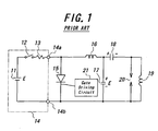
generating a pulse having a high voltage and a large current. Fig. 1
shows an example of a known pulse generating circuit used as a
voltage supply source for use in a pulse laser. In this pulse
generating circuit, between output terminals 14a and 14b of a
charging circuit 14 including a DC power supply source 11, a switch
12 and a current limiting resistor 13, is connected a static induction
thyristor 15 (herein after abbreviated as SIThy). In parallel with the
SIThy 15, there are connected resonance coil 16 and capacitor 17.
Furthermore, in parallel with the capacitor 17 are connected a
capacitor 18 and a coil 19 having a large inductance, and a discharge
gap 20 is connected across the coil 19 as a load.
-
Under a non-conductive condition of the SIThy 15, at first
the switch 12 is closed to charge the capacitor 17 through the resistor
13 and coil 16. During this charging process, an impedance of the
coil 19 at a lower frequency is low, and thus the capacitor 18 is also
charged through the coil 19. Now an output voltage of the DC power
supply source 11 is denoted by E. After charging the capacitors 17
and 18 up to E, the SIThy 15 is turned-on by means of a gate driving
circuit 21. Then, charge stored in the capacitor 17 is discharged
through the SIThy 15 in accordance with a resonance characteristic
determined by the coil 16 and capacitor 17, and the capacitor 17 is
charged in a reverse polarity to a polarity in which the capacitor 17 is
charged up to substantially -E. Charge stored in the capacitor 18 is
also discharged through the SIThy 15 and coil 19. Since an
impedance of the coil 19 is very high for a high frequency, the
discharge is conducted very slowly. Therefore, a voltage of about -
2E will be applied across the discharge gap 20. When a discharge
occurs, charge stored in the capacitors 17 and 18 disappears by
discharge at the discharge gap 20. And the switch 12 is closed to
initiate the charging operation again.
-
In the above mentioned pulse generating circuit, if the
discharging operation is carried out correctly between the discharge
gap 20 when a voltage of -2E is applied across the discharge gap,
charge stored in a resonance circuit consisting of the coil 16 and
capacitor 17 disappears. Therefor, as shown by a solid line in Fig. 2,
no current flows through the SIThy 15 in the reverse direction.
However, if discharge does not occur correctly due to any reason, a
ringing current occurs in the resonance circuit and a large current
flows through the SIThy 15 in the reverse direction as illustrated by a
broken line in Fig. 2.
-
Fig. 3 is a graph showing a voltage across the anode-cathode
path of the SIThy 15. When discharge does not occurs correctly, a
reverse voltage is applied to the SIThy 15. In this case, a reverse
current flows from the cathode to the gate of the SIThy 15, and this
results in application of an excessive high reverse voltage like as a
reverse recovery phenomenon of the diode.
-
In order to protect the static induction thyristor from the
breakdown when the large reverse current flows through the anode-cathode
path of the thyristor, it has been proposed to flow the reverse
current through a diode connected in anti-parallel with the static
induction thyristor. The static induction thyristor having such a
diode is generally called a reverse conducting static induction
thyristor. In the reverse conducting static induction thyristor, in
order to make a wiring inductance as small as possible, it has been
proposed to form the diode by a common semiconductor substrate
together with the static induction thyristor in a preliminary thesis
issued for 1999 Conference of the Electric Engineering Society by
Shimizu et al., "4000V Class Reverse Conducting SI Thyristor(1)".
-
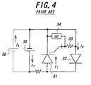
Fig. 4 is an equivalent circuit of the above mentioned
reverse conducting static induction thyristor. A diode 32 is connected
in anti-parallel with a static induction thyristor (SIThy) 31 such that an
anode of the diode is connected to a cathode of the SIThy and a cathode
of the diode is connected to an anode of the SIThy. The anode of the
diode 32 is further connected to a gate of the SIThy 31 by means of a
resistor 33, and the gate of the SIThy is connected to a gate driving
circuit (GC) 34 which controls the turn-on/turn-off of the SIThy.
When a main power supply source 35 is connected across the anode-cathode
path of the SIThy 31 as shown by a solid line in Fig. 4, a
current IT flows through the SIThy, and when a voltage supply source
36 is connected in a reverse polarity as depicted by a broken line in
Fig. 4, a current IR flows through the diode 32 to protect the SIThy 31
from being breakdown.
-
Fig. 5 is a cross sectional view showing the structure of the
above mentioned known reverse conducting static induction thyristor.
In one major surface of an n- silicon substrate 41 there is formed a p+
gate regions 43, and p+ buried gate regions 44 are formed within a
channel region. A gate electrode 45 is provided on the gate region
42 via a conductive layer 45a. The buried gate regions 43 are
formed as a comb shape to be surrounded by the gate region 42.
Above the channel region, there are formed n+ cathode regions 46
which are electrically connected to a cathode electrode 47 via a
conductive layer 47a. On the other major surface of the silicon
substrate 41, an anode electrode 52 is provided via a conductive layer
52a. In this manner, a thyristor section 44 is constructed by the gate
region 42, buried gate regions 43, channel region, cathode regions 46.
Furthermore, a diode section 49 is formed to surround the thyristor
section 44 via a separation band 48. The diode second includes a p+
anode region 50 and a cathode region 41a formed by a part of the n-
silicon substrate 41. The anode region 50 is electrically connected to
the cathode electrode 47 of the static induction thyristor via a
conductive layer 47a and the cathode region 41a is connected to an
anode electrode 52 of the static induction thyristor by means of n+
contact region 51 and conductive layer 52a.
-
In the above explained reverse conducting static induction
thyristor, when a reverse voltage is applied across the anode-cathode
main current path, the diode section 49 is made conductive to prevent
the thyristor section 44 from the breakdown. However, when the
known reverse conducting thyristor is used in the above mentioned
pulse generating circuit shown in Fig. 1, the static induction thyristor
is often broken by the ringing current generated in the resonance
circuit by failure of discharge. In order to investigate a mechanism
of such a phenomenon, the inventors have conducted a detailed
analysis about the influence of the application of the reverse voltage
across the anode-cathode path of the reverse conducting static
induction thyristor.
-
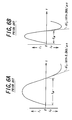
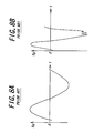
Figs. 6, 7 and 8 are graphs showing the operation of the
static induction thyristor used in the pulse generating circuit upon
occurrence of discharge failure. Fig. 6 represent a variation of a
current Iak flowing through the anode-cathode path, Fig. 7 shows a
variation of a gate current Ig and Fig. 8 denotes a variation of a gate
voltage Vg. In these figures, A represents a case in which a pulse
duration tw is long, and B shows a case in which a pulse duration tw is
long. When the current Iak is larger than 3000 A and the pulse
duration tw is longer than several tens µs, breakdown of the reverse
conducting static induction thyristor does not occur. However, when
a pulse duration tw is set to a shorter value within a range from
several hundreds ns to several µs, the reverse conducting static
induction thyristor might be broken. In this case, a breakdown point
situates in the static induction thyristor section and no abnormal
phenomenon occurs in the diode section. From these phenomena, it
is assumed that the breakdown of the reverse conducting static
induction thyristor depends on an inclination of a raising portion of
the current Iak. In the longer pulse duration shown in Fig. 6A, an
inclination of a reverse current ir (dir/dt) is about 0.5 KA/µs, and in
the shorter pulse duration illustrated in Fig. 6B, an inclination of the
reverse current is about 3 KA/µs. Furthermore, as depicted in
Fig. 8B, when the breakdown of the reverse conducting static
induction thyristor due to discharge failure occurs, a remarkable
variation appears in the gate voltage Vg immediately after a reverse
voltage peak.
-
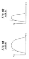
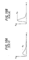
Next the performance of the diode upon an occurrence of an
abruptly increase in the current flowing through the diode is analyzed.
Figs. 9 and 10 show a forward current IF flowing through the anode-cathode
path of the diode 32 shown in Fig. 4 and a forward voltage
drop VF appearing across the anode-cathode path of the diode when
the diode is operated by a pulse. A denotes a case of a smaller
inclination and B represents a case of s larger inclination. From
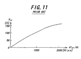
these graphs it can be understood that there is an intimate correlation
between the inclination of the raising portion of the current IF and a
transient on-voltage (forward recovery voltage) VFP as shown in
Fig. 11. That is to say, for the diode having the breakdown voltage
of 4000 V, when the inclination of the current IF (dIF/dt) is about
500 A/µs, the forward recovery voltage VFP is lower such as about
70 V, but when the inclination of the current (dIF/dt) is high such as
1000A/µs and 2000A/µs, the forward recovery voltage VFP is becomes
higher such as about 100 V and 170 V, respectively.
-
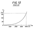
Fig. 12 is a graph showing a relationship between the forward
recovery voltage VFP and the breakdown voltage of the diode for the
inclination dIF/dt of 2000 A/µs. In accordance with the increase in
the diode breakdown voltage, the forward recovery voltage VFP
becomes higher. When the diode has a breakdown voltage of 4000 V,
the forward recovery voltage VFP is about 170 V. In the reverse
conducting static induction thyristor, the breakdown voltage of the
diode section should be not lower than the breakdown voltage of the
thyristor section, and therefore the diode section should have the
breakdown voltage of several thousands volts. The diode section
having such a high breakdown voltage also has a high forward
recovery voltage VFP. In other words, the higher the breakdown
voltage of the diode section is, the forward pulse current hardly flows
through the diode section.
-
In the manner explained above, in the known reverse
conducting static induction thyristor having a breakdown voltage of,
for instance 4 KV, when a large reverse current is to flow immediately
after conducting a large forward current, the protection diode section
could not be made conductive, and a large amount of carriers stored in
the channel regions in Fig. 5 flow abruptly in the reverse direction
from the cathode region 46 to the buried gate region 43. Particularly,
in a region denoted by X in Fig. 5, i.e. in a vicinity of the buried gate
region 43 into which the gate current is supplied much more abruptly
than the central gate region 42, an excessive amount of carriers are
generated and there is produced a filamentation between the channel
regions by the diode reverse recovery phenomenon of the diode
section and the thyristor section 44 might be destroyed.
-
It should be noted that the above explained problem occurs
not only in the reverse conducting static induction thyristor, but also
in a semiconductor switching device such as normal type thyristor,
gate turn-off (GTO) SCR and insulated gate bipolar transistor (IGBT).
Summary of the Invention
-
The present invention has for its object to provide a novel
and useful semiconductor device, in which the above mentioned
problem of the known reverse conducting static induction thyristor,
and even if a high reverse voltage is applied to a switching element
abruptly, a protection diode can be brought into conductive and the
switching element can be effectively protected from the breakdown.
-
According to the invention, a semiconductor device having
reverse conducting faculty comprises:
- a switching element including a semiconductor substrate of a
first conductivity type having first and second major surfaces, a first
main electrode region of the first conductivity type formed in the first
major surface of the semiconductor substrate, a first main electrode
connected to said first main electrode region, a second main electrode
region of a second conductivity type formed in the second major
surface of the semiconductor substrate, a second main electrode
connected to said second main electrode region, a control electrode
region of the second conductivity type formed in the first major
surface of the semiconductor substrate for controlling a current
passing between the first and second main electrode regions, and a
control electrode connected to said control region; and
- a series arrangement of a plurality of diodes connected between
said first main electrode and said second main electrode in an
opposite polarity to a current flowing between said first main
electrode region and said second main electrode region, each of said
plurality of diodes having a breakdown voltage lower than a
breakdown voltage of said switching element.
-
-
Upon practicing the semiconductor device according to the
present invention, it is preferable that said series arrangement of a
plurality of diodes is formed in said first major surface of the
semiconductor substrate in which said first main electrode region is
also formed. Such a structure is particularly suitable for a high
frequency pulse circuit in which inductance of wiring has to be
reduced as far as possible. According to the invention, said series
arrangement of a plurality of diodes may be formed on a separate
semiconductor substrate from said semiconductor substrate semiconductor
substrate which constitutes said switching element, or said
series arrangement of a plurality of diodes may be formed as a diode
stack including first and second electrodes connected to said first and
second main electrodes of the switching element, respectively.
-
In the latter two cases, it is preferable that said switching
device and series arrangement of a plurality of diodes are installed in
a common package in view of a reduction of wiring inductance.
However, according to the invention, said switching device and series
arrangement of a plurality of diodes may be in separate packages.
-
In a preferable embodiment of the semiconductor device
according to the present invention, said switching element is formed
as a static induction thyristor whose cathode region and cathode
electrode are formed by said first main electrode region and first main
electrode, respectively, whose anode region and anode electrode are
formed by said second main electrode region and second main
electrode, respectively, and whose gate region and gate electrode are
formed by said control region and control electrode, respectively.
-
In another preferable embodiment of the switching device
according to the invention, said switching element is formed as a
reverse conducting static induction thyristor including
- a thyristor section whose cathode region and cathode electrode
are formed by said first main electrode region and first main electrode,
respectively, whose anode region and anode electrode are formed by
said second main electrode region and second main electrode,
respectively, and whose gate region and gate electrode are formed by
said control region and control electrode, respectively; and
- a main diode section having an anode region connected to said
cathode electrode of the thyristor section and a cathode region
connected to said anode electrode of the thyristor section.
-
-
In these preferable embodiments, said series arrangement of
a plurality of diodes are preferably formed as field limiting rings
surrounding said static induction thyristor. In this case, a plurality
of diodes of said series arrangement may be preferably formed such
that breakdown voltages of the diodes are gradually increased toward
outside.
Brief Description of the Drawings
-
- Fig. 1 is a circuit diagram showing an example of a known
pulse generating circuit using a static induction thyristor;
- Figs. 2 and 3 are graphs illustrating the operation of the
thyristor shown in Fig. 1;
- Fig. 4 is a schematic diagram depicting a principal structure
of a known reverse conducting static induction thyristor;
- Fig. 5 is a cross sectional view showing a detailed structure
of the known reverse conducting thyristor;
- Figs. 6A, 6B; 7A, 7B and 8A, 8B are signal waveforms
explaining the operation of the known reverse conducting static
induction thyristor;
- Figs. 9A and 9B are signal waveforms representing a
forward recovery characteristic of the known reverse conducting static
induction thyristor;
- Figs. 10A and 10B are signal waveforms denoting a
transient turn-on voltage of the known reverse conducting static
induction thyristor;
- Fig. 11 is a graph expressing a relationship between an
inclination of a current and a forward recovery voltage of a diode;
- Fig. 12 is a graph showing a relationship between a
breakdown voltage and a forward recovery voltage of a diode;
- Fig. 13 is a schematic diagram illustrating a principal
structure of the semiconductor device according to the invention;
- Fig. 14 is a schematic diagram depicting another principal
structure of the semiconductor device according to the invention;
- Fig. 15 is a cross sectional view showing a detailed structure
of a first embodiment of the semiconductor device according to the
invention;
- Fig. 16 is an enlarged cross sectional view of a part of the
semiconductor device shown in Fig. 15;
- Fig. 17 is a cross sectional view showing a detailed structure
of a second embodiment of the semiconductor device according to the
invention;
- Fig. 18 is an enlarged cross sectional view of a part of the
semiconductor device shown in Fig. 17;
- Fig. 19 is a cross sectional view illustrating a detailed
structure of a third embodiment of the semiconductor device
according to the invention;
- Fig. 20 is a cross sectional view depicting a detailed
structure of a fourth embodiment of the semiconductor device
according to the invention; and
- Fig. 21 is a graph representing test results of the semiconductor
device according to the invention in comparison with the
known reverse conducting thyristor.
-
Description of the Preferred Embodiments
-
Now the present invention will be explained in detail with
reference to several embodiments shown in the accompanying
drawings.
-
Fig. 13 is a schematic diagram showing a principal structure
of the semiconductor device according to the invention. As explained
above, according to the invention, the switching element may be
formed not only by a static induction thyristor, but also by another
semiconductor switching element such as SCR and IGBT. For the
sake of explanation, hereinafter the switching element is formed by a
static induction thyristor.
-
According to the invention, between an anode A and a
cathode K of a static induction thyristor 61, is connected a series
arrangement 63 of a plurality of diodes 62 is connected such that an
anode of the series arrangement of diodes 63 is connected to the
cathode K of the static induction thyristor 61 and a cathode of the
series arrangement of diodes is connected to the anode A of the static
induction thyristor, each of said plurality of diodes 62 having a
breakdown voltage which is lower than a breakdown voltage of the
static induction thyristor 61. That is to say, the series arrangement
63 of diodes 62 is connected in parallel with the static induction
thyristor in a reverse polarity. The breakdown voltages of these
diodes 62 are set such that a sum of breakdown voltages of respective
diodes becomes not less than the breakdown voltage of the static
induction thyristor 61.
-
For instance, now it is assumed that all the diodes 62 have
the same characteristics and the static induction thyristor 61 has the
breakdown voltage of 4000 V, then eight diodes each having a
breakdown voltage of 500 V may be connected in series. In this case,
as can be understood from Fig. 12, the forward recovery voltage VFP
of each diodes becomes about 10 V. Even if eight diodes are
connected in series, a total forward recovery voltage of the series
arrangement of diodes becomes 80 V(=10x8) which is sufficiently
lower than the forward recovery voltage of about 170 V of a single
diode having a breakdown voltage of 4000 V. When a reverse
current is to be flown abruptly through the anode-cathode path of the
static induction thyristor 61, the series arrangement 63 of diodes 62
are conducted. Therefore, the reverse current flowing through the
static induction thyristor 61 is reduced and a high reverse voltage is
not applied to the static induction thyristor. In this manner, the static
induction thyristor 61 can be effectively protected against the
breakdown.
-
Fig. 14 is a schematic diagram illustrating another principal
structure of the semiconductor device according to the invention.
In this structure, the static induction thyristor is constructed as the
reverse conducting static induction thyristor having a static induction
thyristor section 61 and a diode section 64 connected in parallel with
the static induction thyristor section 61 in a reverse polarity.
Furthermore, a series arrangement 62 of a plurality of diodes 62 is
connected in parallel with the reverse conducting static induction
thyristor.
-
The semiconductor device according to the invention having
the above explained principal structures may be embodied in various
ways. For instance, the series arrangement 63 of a plurality of
diodes 62 may be formed on a same semiconductor substrate of the
static induction thyristor 61 as a single unit. Particularly, when the
semiconductor device is used in a high frequency circuit, it is
necessary to make a stray inductance of wiring conductors as small as
possible, and therefore it is preferable to construct the static induction
thyristor 61 and series arrangement 63 of a plurality of diodes 62 in a
single common semiconductor substrate. Furthermore, in the semiconductor
device according to the invention, the series arrangement
63 of a plurality of diodes 62 may be constructed separately from a
semiconductor substrate on which the static induction thyristor 61 is
formed. In this case, the series arrangement 63 of diodes is
preferably arranged within a package in which the static induction
thyristor 61 is arranged, but it may be provided outside the package.
This type of structure may be advantageously applied to the known
semiconductor devices such as the static induction thyristor 61 shown
in Fig. 13 and the reverse conducting static induction thyristor having
the static induction thyristor 61 and the single diode 64 illustrated in
Fig. 14.
-
Figs. 15 and 16 are cross sectional views illustrating a first
embodiment of the semiconductor device according to the invention
having the principal structure shown in Fig. 14, in which the series
arrangement 63 of a plurality of diodes 62 is connected in parallel
with the switching element, i.e. static induction thyristor 61 as well as
the single diode 64. A p+ gate region (control region) 102 is formed
substantially at a center area of one major surface of an n- silicon
substrate 101, a plurality of first ring-shaped recesses 103 are formed
to surround the gate region 102, and gate regions 104 are formed
along the recesses 103. Furthermore, buried gate regions 105 are
formed in channel regions formed by parts of the silicon substrate 101
surrounded by successive gate regions 102 and 104. On the gate
regions 102 and 104 are formed conductive layers 106 and a gate
electrode 107 is provided on the conductive layer at the central gate
region 102. In surface portions of the channel regions, there are
formed n+ cathode regions (one major electrode region) 108 and the
cathode regions are connected to a cathode electrode 110 via
conductive layers 109. In the other major surface of the silicon
substrate 101, there are formed p+ anode regions (the other major
electrode region) 111, which are connected to an anode electrode 113
via a conductive layer 112. In this manner, the thyristor section 114
is constructed.
-
In the first major surface of the silicon substrate 101, there
is formed a single ring-shaped second recess 121 and a plurality of
ring-shaped p+ regions 122 are formed on a bottom of the second
recess to construct a separation band 123.
-
Outside the separation band 123, there is formed a p+ anode
region 131 of a main diode 134, said anode region having a wider
width than the remaining p+ regions 104 in the thyristor section 114.
The anode region 131 is connected to the cathode electrode 110 via a
conductive layer 132 of the thyristor section 114. A cathode region
of the main diode section 134 is formed by a bulk of the n- silicon
substrate 101 situating under the anode region 131. In the second
major surface of the silicon substrate 101 at a portion corresponding
to the anode region 131, there is formed an n+ emitter region 133,
which is connected to the anode electrode 113 of the thyristor section
144. In this manner, the main diode section 134 serving to protect
the thyristor section from the breakdown is formed such that the main
diode section 134 is connected in parallel with the thyristor section
114 in a reverse polarity.
-
The structure of the thyristor section 114, separation band
123 and main diode section 134 is identical with that of the known
reverse conducting static induction thyristor. According to the
present invention, in the first major surface of the silicon substrate
101, there are formed a plurality of ring-shaped third recesses 141 are
formed to surround the main diode section 134, and in bottoms of
these third recesses there are formed p+ anode regions 142. As clearly
illustrated in Fig. 16, each of the anode regions 142 is formed at a
position deflected toward one side of the third recess 141. Between
successive third recesses 141 there are formed n+ cathode contact
regions 143, and the successive cathode regions 143 are connected to
adjacent p+ anode regions 142 successively to constitute a series
arrangement of a plurality of diodes by means of conductive layers
144. In this manner, a series arrangement section 145 is formed.
Although not shown in Fig. 15, exposed portions of the first major
surface of the silicon substrate 101 are covered with insulating layers
146 such as silicon oxide layers as shown in Fig. 16.
-
As illustrated in Fig. 15, an anode region of the innermost
diode in the series arrangement section 145 is formed by the anode
region 131 of the main diode section 34, and a cathode of the
outermost diode is connected to the anode electrode 113 of the static
induction thyristor by means of the outermost cathode contact region
143 and conductive layers 147 and 112. In this manner, there is
formed the series arrangement section 145, in which the anode of the
innermost diode is connected to the cathode electrode 110 of the
thyristor and the cathode of the outermost diode is connected to the
anode electrode 113. The main diode section 134 is connected in
parallel with the series arrangement section 145 of a plurality of
diodes.
-
In the semiconductor device of the present embodiment,
each of the plural diodes of the series arrangement section 145 has a
breakdown voltage which is sufficiently lower than a breakdown
voltage of the main diode section 134, and therefore its forward
recovery voltage is sufficiently lower than that of the main diode
section and energy loss due to the forward conduction becomes also
very small. When a reverse voltage is applied to the thyristor section
114, at first a plurality of diodes in the series arrangement section 145
are made conductive, and then the main diode section 134 is made
conductive. In this manner, the thyristor section 134 can be
effectively prevented from the breakdown.
-
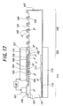
Figs. 17 and 18 are cross sectional views illustrating a
second embodiment of the semiconductor device according to the
invention. In the present embodiment, the switching element is
formed by the static induction thyristor without the main diode, and
portions similar to those of the first embodiment are denoted by the
same reference numerals used in Figs. 15 and 16. The ring-shaped
recesses 141 formed in the series arrangement section 145 of a
plurality of diodes are formed such that successive recesses viewed
from the internal one have increasing widths so that the successive
diodes have increasing breakdown voltage. Then, the p+ anode
regions 142 of these diodes serve optimally as a field limiting ring.
-
Also in the first embodiment illustrated in Figs. 15 and 16,
the anode regions of a plurality of diodes of the series arrangement
section 145 serve as the field limiting ring to some extent, but they do
not optimally operate as the field limiting ring, because the third
recesses 141 have identical width. In the present embodiment, the
third recesses 141 formed in the series arrangement section 145 of a
plurality of diodes have widths which are successively increased
toward outside such that the p+ anode regions 142 of the diodes work
optimally as the field limiting ring. Such a structure may be easily
realized by a known field limiting ring designing method.
-
Fig. 19 is a cross sectional view showing a third embodiment
of the semiconductor device according to the invention. Like
as the second embodiment, in the present embodiment, the switching
element is formed by the static induction thyristor without a main
diode. That is to say, in the first embodiment, the series arrangement
section 145 of a plurality of diodes is provided in addition to the main
diode section 134, but in the present embodiment the main diode
section is not provided. In the present embodiment, a p+ anode
region of the innermost diode within the series arrangement 145 of a
plurality of diodes is constituted by a p+ region 122 within the separation
band 123. The remaining structure of the present embodiment is
identical with the above mentioned second embodiment.
-
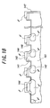
Fig. 20 is a cross sectional view of a fourth embodiment of
the semiconductor device according to the invention. In this embodiment,
the switching element is formed by the reverse conducting
thyristor. In the embodiments so far explained, the series arrangement
of diodes is formed on the silicon substrate on which the
thyristor is also formed. In the present embodiment, only the
thyristor section 114, separation band 123 and main diode section 134
are formed on the silicon substrate 101, and a series arrangement 152
of a plurality of diodes 151 is provided separately from the silicon
substrate 101. It should be noted that in Fig. 20, a reference numeral
161 denotes a field limiting ring section.
-
In this case, the series arrangement of diodes may be formed
on a semiconductor wafer like as the previous embodiment, but in the
present embodiment, the series arrangement 152 of a plurality of
diodes 151 is constructed by a diode stack. Furthermore, in the
present embodiment, respective diodes 151 is constructed to have P+-i-n+
structure and the series arrangement 152 is beveled such that a
surface area of the diodes 151 is gradually decreased from the anode
side to the cathode side. An anode electrode 153 of the series
arrangement 152 of a plurality of diodes 151 is connected to the
cathode electrode 110 of the thyristor section 114 and a cathode
electrode 154 is connected to the anode electrode 113 of the thyristor
section 114. The series arrangement 152 of a plurality of diodes 151
is preferably installed within a common package together with the
silicon substrate 101 of the reverse conducting thyristor, but it may be
installed in a separate package.
-
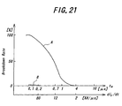
Fig. 21 is a graph representing a breakdown rate of the
semiconductor device according to the invention in comparison with
the known reverse conducting static induction thyristor. In the
known reverse conducting static induction thyristor having only the
main diode, the breakdown occurs in almost all samples when a width
of a pulse voltage applied to the thyristor is not longer than 0.1 µs, i.e.
when an inclination of a reverse current is not smaller than about
100 KA/µs as shown by a curve A, and the breakdown occurs in a
substantially half number of the samples at about 12 KA/µs. In the
semiconductor device according to the invention, no breakdown
occurs in all samples even when the reverse current having an abrupt
inclination not smaller than 100 KA/µs flows as depicted by a curve B.
In this test, a peak value of the forward current is set to 4000 A.
-
It should be noted that the present invention is not limited to
the embodiments explained above, but many alternations and
modifications may be conceived by a person skilled in the art within
the scope of the invention defined by claims. For instance, in the
above embodiments, the switching element formed on the semiconductor
substrate is constituted by the static induction thyristor, but
according to the invention, the switching element may be formed by
any other switching element such as the gate turn-off (GTO) SCR and
insulated gate bipolar transistor (IGBT). The number of diodes
within the series arrangement for use in the pulse generating circuit
may be determined at will taking into account of breakdown voltage
of the thyristor as well as breakdown voltages of respective diodes.
-
As stated above in detail, in the semiconductor device
according to the present invention, since the series arrangement of a
plurality of diodes is connected in parallel with the switching element
in a reverse polarity and each of these diodes has a breakdown voltage
lower than a breakdown voltage of the switching element, when a
current flowing through the switching element is abruptly decreased
and a large reverse voltage is applied to the switching element, the
series arrangement of diodes is positively conducted and the switching
element can be-effectively prevented from breakdown.
-
Moreover, in the above embodiment in which the anode
regions of a plurality of diodes are constructed to serve as the field
limiting rings, the series arrangement of diodes can be formed as a
substantially same size as a conventional semiconductor device
having the field limiting rings. Therefore, an increase in
manufacturing cost can be restricted and an increase in cost of the
semiconductor device according to the invention can be limited.