EP1125326B1 - Selectively doped trench device isolation - Google Patents
Selectively doped trench device isolation Download PDFInfo
- Publication number
- EP1125326B1 EP1125326B1 EP99957461A EP99957461A EP1125326B1 EP 1125326 B1 EP1125326 B1 EP 1125326B1 EP 99957461 A EP99957461 A EP 99957461A EP 99957461 A EP99957461 A EP 99957461A EP 1125326 B1 EP1125326 B1 EP 1125326B1
- Authority
- EP
- European Patent Office
- Prior art keywords
- trench
- substrate
- layer
- isolation device
- work function
- Prior art date
- Legal status (The legal status is an assumption and is not a legal conclusion. Google has not performed a legal analysis and makes no representation as to the accuracy of the status listed.)
- Expired - Lifetime
Links
Images


Classifications
-
- H—ELECTRICITY
- H01—ELECTRIC ELEMENTS
- H01L—SEMICONDUCTOR DEVICES NOT COVERED BY CLASS H10
- H01L21/00—Processes or apparatus adapted for the manufacture or treatment of semiconductor or solid state devices or of parts thereof
- H01L21/70—Manufacture or treatment of devices consisting of a plurality of solid state components formed in or on a common substrate or of parts thereof; Manufacture of integrated circuit devices or of parts thereof
- H01L21/77—Manufacture or treatment of devices consisting of a plurality of solid state components or integrated circuits formed in, or on, a common substrate
- H01L21/78—Manufacture or treatment of devices consisting of a plurality of solid state components or integrated circuits formed in, or on, a common substrate with subsequent division of the substrate into plural individual devices
- H01L21/82—Manufacture or treatment of devices consisting of a plurality of solid state components or integrated circuits formed in, or on, a common substrate with subsequent division of the substrate into plural individual devices to produce devices, e.g. integrated circuits, each consisting of a plurality of components
- H01L21/822—Manufacture or treatment of devices consisting of a plurality of solid state components or integrated circuits formed in, or on, a common substrate with subsequent division of the substrate into plural individual devices to produce devices, e.g. integrated circuits, each consisting of a plurality of components the substrate being a semiconductor, using silicon technology
- H01L21/8232—Field-effect technology
- H01L21/8234—MIS technology, i.e. integration processes of field effect transistors of the conductor-insulator-semiconductor type
- H01L21/823481—MIS technology, i.e. integration processes of field effect transistors of the conductor-insulator-semiconductor type isolation region manufacturing related aspects, e.g. to avoid interaction of isolation region with adjacent structure
-
- H—ELECTRICITY
- H01—ELECTRIC ELEMENTS
- H01L—SEMICONDUCTOR DEVICES NOT COVERED BY CLASS H10
- H01L21/00—Processes or apparatus adapted for the manufacture or treatment of semiconductor or solid state devices or of parts thereof
- H01L21/70—Manufacture or treatment of devices consisting of a plurality of solid state components formed in or on a common substrate or of parts thereof; Manufacture of integrated circuit devices or of parts thereof
- H01L21/71—Manufacture of specific parts of devices defined in group H01L21/70
- H01L21/76—Making of isolation regions between components
- H01L21/763—Polycrystalline semiconductor regions
-
- H—ELECTRICITY
- H01—ELECTRIC ELEMENTS
- H01L—SEMICONDUCTOR DEVICES NOT COVERED BY CLASS H10
- H01L21/00—Processes or apparatus adapted for the manufacture or treatment of semiconductor or solid state devices or of parts thereof
- H01L21/70—Manufacture or treatment of devices consisting of a plurality of solid state components formed in or on a common substrate or of parts thereof; Manufacture of integrated circuit devices or of parts thereof
- H01L21/71—Manufacture of specific parts of devices defined in group H01L21/70
- H01L21/76—Making of isolation regions between components
- H01L21/765—Making of isolation regions between components by field effect
Definitions
- the present invention relates to semiconductor device design and fabrication and more particularly to trench isolation of such devices.
- Such ICs generally consist of an array of active devices such as transistors or capacitors.
- each of the capacitors and transistors are separated by an isolation structure that is adapted to electrically isolate adjacent active devices from each other.
- an isolation structure that is adapted to electrically isolate adjacent active devices from each other.
- the integrity and the reliability of each active device greatly depends on ability to electrically isolate each active device from adjacent active devices as leakage currents from adjacent devices can result in failure.
- each isolation structure must still maintain the required degree of isolation to prevent leakage currents between the individual active devices.
- Active devices on a chip are generally spaced apart by the regions known as field regions in which the isolation structures are formed.
- isolation between the active devices is achieved by interposing the isolation structure, normally called a field device, therebetween to interrupt the parasitic conduction.
- a difference in potential between adjacent active devices induces charge carriers to travel between the two active devices.
- the difference in potential is referred to as the threshold voltage required to produce this parasitic conduction.
- the isolation structure used to inhibit parasitic conduction is formed out of a generally nonconductive oxide material, such as silicon oxide.
- the presence of the isolation structure increases the threshold voltage necessary to produce parasitic conduction to a point where the difference in potential between adjacent active devices never reaches the threshold voltage.
- This threshold voltage in the context of isolation structures, is commonly referred to as the field threshold.
- the threshold voltage resulting from the formation of the isolation structure is proportionate to the thickness of the isolation structure. Hence, the thicker the structure, the greater the threshold voltage which results in less parasitic conduction during active device operation.
- the mechanism of parasitic conduction between active devices can be viewed as a parasitic device that is established between active devices.
- the parasitic device is analogous in operation to a field effect transistor. Consequently, the isolation structure, acting as a gate in a field effect transistor, increases the threshold voltage of the parasitic devices that spontaneously exist between the active devices and prevents inadvertent electrical coupling between the active devices.
- the goal in any isolation scheme is to make this field threshold voltage as high as possible without adversely effecting the characteristics of adjacent devices. In the semiconductor industry, this is conventionally done by forming thick isolation structures in the field regions.
- Such isolation structures are conventionally formed using processes such as LOCOS (For LOCalized Oxidation of Silicon) or trench isolation.
- LOCOS Form LOCalized Oxidation of Silicon
- thick isolation structures known as field oxide regions are formed by oxidizing the regions between adjacent active devices.
- the high field threshold provided by such thick field oxide effectively isolates the active devices
- the LOCOS process presents some disadvantages associated with the nature of the oxidation process. For example, thick isolation structures formed through oxidation consume a considerate amount of area on the chip limiting the amount of area available for active devices and thereby limiting the active device density.
- This lateral encroachment is known as bird's beak encroachment and it further limits the size of the active areas of the chip and the active device density. This bird's beak encroachment remains a significant problem even as device dimensions and isolation structure dimensions are decreased to accommodate higher active device densities.
- trench isolation One alternative to the LOCOS process is known as trench isolation.
- Examples of devices utilising trench isolation are disclosed in US-A-5 179 038 (Kinney Wayne I et al), EP-A-0 220 108 (Thomson components Mostek Corp), US-A-4 470 062 (Muramatsu Akira), JP 62 131539 A (Fujitsu Ltd.) and JP 01 138730 A (Fujitsu Ltd.).
- trench isolation processes do not experience bird's beak lateral encroachment and resulting active area loss.
- Trench isolation generally involves etching a trench in the substrate between the active devices and filling the trench with an insulator such as silicon oxide. In order to provide high field threshold voltages and to prevent the formation of a conductive channel between neighboring active devices, the trench must have a sufficient depth and width.
- trench isolation techniques generally do not have the lateral encroachment problems associated with LOCOS isolation structures, trench isolation structures must still have relatively large minimum dimensions to maintain adequate isolation between adjacent active devices which inhibits significant increase in device density on an integrated circuit.
- Channel-stop implants are usually the same dopant type as the dopant type of the substrate, but channel stop implants are implanted in higher doping concentrations to effectively limit the channel formation.
- doping trench walls is a tedious and technically difficult process, and the doped implant often has a tendency to diffuse into active device regions, resulting in undesirable changes in device characteristics.
- US 5179038 describes a trench isolation structure with highly doped polysilicon in a trench connected to the substrate.
- EP 220108 discloses isolation trenches filled with p++ polysilicon in a p-type substrate.
- US 4,470,062 describes a device with grounded polysilicon trench on a p-type substrate.
- trench isolation method fills the trench with polysilicon.
- device isolation can be achieved by applying a low bias to the polysilicon so as to prevent channel formation between the active devices.
- the field threshold voltage of these isolation structures may not be adequately high enough to prevent channel formation.
- poly filled trenches may still require side wall channel stop implants.
- isolation structures having high field threshold voltages and improved isolation characteristics so as to provide isolation between adjacent active devices in higher active device density applications.
- isolation structures that reduce channeling between adjacent devices but do not require time consuming doping processes to achieve adequately isolating structures.
- the present invention is comprised of an isolation structure formed in a substrate of a semiconductor material having a first work function, the isolation structure comprising a trench formed in the substrate with an insolation layer positioned on the trench surfaces and a material having a second work function, higher than the first work function, that is positioned inside of the trench on the exposed surface of the insulating layer.
- the isolation material is of the same dopant type as the substrate but has a higher dopant concentration.
- the isolation material is formed of a material that can be biased so as to increase the threshold voltage of the isolation structure.
- a method of forming an isolation structure is provided.
- the method is comprised of forming a trench in a substrate of a first work function, depositing an isolation or insulating layer on the inner surfaces of the trench and then positioning a material having a second work function, higher than the first work function on the inner surfaces of the isolation or insulating material.
- the isolation material can be biased.
- a trench is formed in a field region of a p-type substrate and a thin layer of field oxide is formed on the trench side walls and the floor.
- the oxide covered trench is then filled with a material having work function value that is higher than the work function value of the p-type substrate.
- the material is a heavily doped P+ polysilicon material.
- the higher work function of the P+ polysilicon material produces a high flat band voltage that produces high threshold voltages.
- This high threshold voltage of the trench isolation device prevents current leakages between the active devices that are separated by the trench isolation device of this invention. Further, this threshold voltage can advantageously be controlled by varying the bias on the gate material.
- the dopant atoms from the polysilicon diffuse through the isolation layer thereby forming a higher doped channel stop region adjacent the interface between the substrate and the isolation region without requiring the use of channel implants or side wall-implants.
- Figure 1 illustrates a semiconductor substrate 100 where a mask structure 102 is formed on a top surface 104 of the substrate 100.
- the semiconductor substrate 100 preferably comprises a p-type silicon substrate, and the mask structure 102 may be comprised of a silicon oxide layer 106 and a nitride layer 108.
- the silicon oxide layer 106 often referred to as pad-oxide layer, may be formed by oxidation of the top surface 104 using any of a number of well-known wet or dry oxidation techniques so as to grow a silicon oxide layer with a thickness on the order of approximately 30 to 300 Angstroms.
- the nitride layer 108 may be formed on the pad-oxide layer 106 using any of a well-known deposition processes, preferably a Chemical Vapor Deposition (CVD) process.
- a resist layer 110 is formed on the nitride layer 108 through conventional resist forming techniques. Thereafter, as illustrated in Figure 3, a trench 112 is formed in the substrate 100 by patterning and defining the resist layer 110, and subsequently etching the masking structure 102 and substrate 100 to form the trench 112 within the substrate 100.
- the patterning and definition of the resist layer 110 can be carried out using any of a well-known conventional photolithographic techniques in the art.
- a selective etch process may initially be used to etch an aperture 114, which has side walls 116, through the mask structure 102.
- the trench 112 is then etched in the substrate through the aperture 114.
- Etching of the substrate 100 continues until a floor 118 of the trench 112 is horizontally formed at a selected depth within the substrate 100, while side walls 120 of the trench 112 extend general vertically downwardly from the interface between the substrate 100 and the mask structure 102.
- Etching of the mask structure 102 and the substrate 100 may be performed using a dry etch technique, such as a Reactive Ion Etching (RIE) technique, in a manner well known in the art of semiconductor processing so that the trench 112 is formed with generally vertical sidewalls 120.
- RIE Reactive Ion Etching
- the resist layer 110 is then removed from the top of the nitride layer 108.
- a layer 122 of a first material may be formed on the floor 118 and the side walls 120 of the trench 112 as well as side walls 116 and the top of the nitride layer 108.
- the first material layer 122 comprises an isolation material layer and is preferably a silicon oxide layer.
- the silicon oxide layer 122 forms the field oxide layer of the gated trench isolation device of this embodiment.
- the silicon oxide layer 122 may be formed using either a well known a deposition or a well known oxidation technique to a thickness range of approximately 50-500 ⁇ depending upon the technology and chip operating voltage.
- a second material 124 is deposited on the field oxide layer 122 so as to fill trench 112, aperture 114 and to cover the top surface of the nitride layer 108. As will also be described further hereinbelow, the second material 124 is connected to the contact element or the gate of the field isolation device of this embodiment.
- the second material 124 comprises a material having a work function value that is higher than the work function value of the material forming the substrate 100 (p-type impurity doped silicon).
- the work function is a specific material parameter which may be defined as a threshold energy required to remove an electron from a material.
- the second material 124 may comprise a selectively heavily p-type impurity doped polysilicon (P+ poly) material having a work function value of approximately 5.2 electron volts.
- the P+ poly material comprises polysilicon with a p-type doping impurity introduced therein, preferably Boron with a preferred doping concentration range of approximately 10 19 - 10 21 atoms cm -3 .
- the second material 124 is used in conjunction with a p-type silicon substrate 100 having a doping concentration of approximately 10 14 - 10 15 atoms cm 3 and a work function of approximately 4.9 electron volts.
- N + poly has a work function value of 4.17 electron volts.
- the second material 124 is then planarized down to the level of a portion of the oxide layer 122 which is on top of the nitride layer 108.
- a chemical mechanical polishing (CMP) process may preferably be used to planarize the second material 124.
- CMP chemical mechanical polishing
- a dry etch process may also be used to remove this second material layer.
- the second material 124 is then further planarized down to the level of the first surface 104 of the substrate 100 preferably removing the nitride layer 108 and the pad oxide 106 so as to reveal the adjacent active areas 126a, 126b and an embodiment of a field isolation device 127 interposed therebetween.
- the field isolation device 127 has the field oxide layer 122 and the second material 124.
- the second material may be selectively dry etched down to the level of the active areas 126a, 126b while the remaining portions of the mask structure 108 protects underlying active areas 105 from being etched. After this etching is complete, the mask structure 108 and the exposed portions of the field oxide layer 122 are removed using suitable dry or wet etch processes.
- the process results in the formation of the isolation structure 127 having the oxide layer 122 on each of the inner surfaces of the trench 112 and the second material 124 positioned inside of the oxide layers 122.
- the P+ poly material comprises a high work function material when compared to the material of the substrate 100 while the N+ poly material comprises a low work function material when compared to the material of the substrate 100.
- the field isolation device 127 is comprised of a isolation material that is positioned within a trench so as to be interposed between two materials (e.g., P+ poly and the substrate) having positively different work functions.
- the work function difference between a metal (or polysilicon) and semiconductor, which both are connected through an oxide interlayer so as to form a metal - oxide - semiconductor structure is generally defined as the flat band vohage of that structure.
- the flat band voltage is a well-known concept to those skilled in the semiconductor art.
- the threshold voltage is a strong function of a flat band voltage. A positively different work function between the P+ poly and the p-doped substrate results in a larger threshold voltage than that of a negatively different work function.
- the field isolation device 127 has an increased field threshold voltage as a result of using materials to form the isolation structure that has a positive work function difference from the material forming the substrate.
- field threshold voltage is the voltage at which an inadvertent current-flow (leakage) between the active devices may occur.
- the resulting high work function difference between the p-doped substrate 100 and the P+ poly material advantageously increases field threshold voltage of the isolation structure thereby preventing shortages between the adjacent devices.
- doping implant in the heavily doped second material 124 will diffuse through the field oxide layer 122 to create a dopant impurity rich region 125 at the interface between the substrate 100 and the field oxide layer 122.
- This dopant rich region 125 acts like a channel stop region further increasing the field threshold voltage and inhibiting leakage across the isolation device 127.
- a channel-stop region further enhances the field threshold voltage and inhibits parasitic conduction.
- the process of the preferred embodiment results in the creation of channel stop implants adjacent the side walls of the isolation device 127 without requiring the use of tedious and expensive channel stop implant techniques. Consequently, the field isolation device 127 of this embodiment may have a field threshold voltage of at least 10 volts.
- a pair of exemplary transistors may be formed on the either side of the field. isolation device 127.
- a contact element 131 is connected to the second material 124 of the field device 127 so that a bias voltage can be applied to the second material 124.
- the contact element can be replaced with a conventional gate structure (not shown) which generally comprises a layer of gate oxide deposited on the second material, and a polysilicon layer deposited on the gate oxide layer.
- the first transistor 128 comprises a gate oxide layer 132a located between a gate electrode 132a and a channel region 136a.
- the transistor 128 also have a source and drain regions 138a and 140a which may be formed as doped diffused regions as in the manner shown in Figure 8.
- the second transistor 130 has a gate oxide layer 132b, a gate electrode 132b, a channel region 136b as well as source and drain regions 138b and 140b.
- the transistors 128 and 130 are formed using methods which are well-known in the semiconductor device manufacturing technologies.
- the field isolation device 127 introduces higher threshold voltages and thus prevents current leakages between the transistors 128 and 130. Further, this threshold voltage can advantageously be controlled by varying the bias on the second material 124.
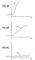
- doped polysilicon isolation structures exhibit superior leakage characteristics compared to that of a silicon oxide (SiO 2) isolation device of the prior art when these devices are tested at an isolation scheme that is similar to one shown in Figure 8.
- the isolation structures can be modeled as a transistor with the isolation device forming a gate and the two active areas forming a drain and a source.
- This undesirably high leakage is due to varying surface potential along the SiO 2 -substrate interface region so that when the device is biased at 0 volts, the potential on this interface, or channel, is not always 0 volts. In such devices, near the drain region, this surface potential is generally greater than zero, thus causing a leakage current from the drain side.
- an N+ poly filled trench device can be formed with the same process used for forming a P + poly filled device (i.e., there is an SiO 2 layer between the N+ poly and the substrate).
- the potential along the SiO 2 -substrate interface region, or channel is almost 0 volts. This, in turn, significantly reduces the leakage currents.
- this leakage current is at least 5 or more orders of magnitude lower than the current leakage that occurred in the prior art trench oxide device down to approximately 6.5E -15 Amperes ⁇ m (current/trench width).
- NMOS metal-oxide-semiconductor
- PMOS metal-oxide-semiconductor
- CMOS complementary metal-oxide-semiconductor
- MOS metal-oxide-semiconductor
Landscapes
- Engineering & Computer Science (AREA)
- Manufacturing & Machinery (AREA)
- Physics & Mathematics (AREA)
- Condensed Matter Physics & Semiconductors (AREA)
- General Physics & Mathematics (AREA)
- Computer Hardware Design (AREA)
- Microelectronics & Electronic Packaging (AREA)
- Power Engineering (AREA)
- Crystallography & Structural Chemistry (AREA)
- Chemical & Material Sciences (AREA)
- Element Separation (AREA)
- Bipolar Transistors (AREA)
- Formation Of Insulating Films (AREA)
- Crystals, And After-Treatments Of Crystals (AREA)
Abstract
Description
Claims (18)
- A trench isolation device comprising:characterized by a contact (131) connected to the second material layer (124) for applying a variable bias to control the threshold voltage of the device.a semiconductor substrate (100) defining active areas (126) and a field region interposed between said active areas (126) wherein said substrate (100) comprises a first implant doping concentration said substrate having a first work function value;a trench (112) formed in said field region, said trench (112) defines a trench surface;a first material layer (122) formed on the floor and the sidewalls of said trench surface wherein said first material layer (122) is comprised of an insulating material; anda second material layer (124) formed on said first material layer (122) wherein said second material layer (124) comprises a material having a second implant doping concentration, said second material layer having a second work function value that is higher than said first work function value to thereby induce a high threshold voltage in said field region of the semiconductor substrate (100);
- The trench isolation device of Claim 1, wherein said substrate (100) is a p-type silicon substrate.
- The trench isolation device of Claim 1 or 2, wherein said first work function value is approximately 4.9 electron volts.
- The trench isolation device of any previous Claim, wherein said second work function value is approximately 5.2 electron volts.
- The trench isolation device of any previous Claim, the work function difference between said second material (124) and said substrate (100) is in the range of approximately +0.3 electron volts.
- The trench isolation device of any previous Claim, wherein said insulating material (122) is silicon dioxide (SiO2).
- The trench isolation device of any previous Claim, wherein said second material (124) is comprised of P+ polysilicon material, said P+ polysilicon material comprises a p-type dopant material.
- The trench isolation device of Claim 7, wherein said p-type dopant material is boron.
- The trench isolation device of Claim 7 or 8, wherein a channel stop layer (125) is formed at an interface between said trench surface and said insulating layer (122) as a result of diffusion of said p-type dopant material from said P+ polysilicon material into said substrate (100).
- The trench isolation device of Claim 10, wherein a channel stop layer (125) is formed at an interface between said trench surface and said insulating layer (122) as a result of diffusion of said n-type dopant material from said N+ polysilicon material into said substrate (100).
- The trench isolation device of any preceding claim wherein said threshold voltage is in the range of at least 10 volts.
- A method of forming an isolation device on a field region of a substrate comprising:forming a trench (112) formed in the substrate (100) wherein said trench (112) defines a trench surface;forming a first material layer (122) on the floor and the sidewalls of said surface wherein said first material (122) is comprised of an insulating material;filling said trench with a second material (124) having a work function value higher than the work function value of the substrate (100); andvarying an electrical bias applied to said second material (124) so as to vary a field threshold voltage into said field region wherein said field threshold voltage inhibits electrical conduction in that field region.
- The method of Claim 12, further comprising forming a mask structure (102) on said substrate prior to forming said trench step.
- The method of Claim 13, further comprising patterning and etching said masking structure (102).
- The method of Claim 13 or 14, wherein the act of forming a mask structure (102) comprises:forming a silicon oxide layer (106) on said substrate (100); anddepositing a nitride layer (108) on said silicon oxide layer.
- The method of any of Claims 12 to 15, wherein said forming a first material layer (122) on said surface comprises growing a silicon oxide layer on said surface.
- The method of Claim 16, wherein the act of said filling said trench (112) comprises selectively depositing a P+ polysilicon material on said silicon oxide layer wherein said P+ polysilicon material comprises a p-type dopant material.
- The method of Claim 17, wherein the act of selectively depositing a P+ polysilicon material on said silicon oxide layer results in forming a channel stop layer (125) between the side walls of said trench and said silicon oxide layer by diffusion of said dopant material into an interface between the side walls of said trench (112) and said silicon oxide layer.
Priority Applications (1)
| Application Number | Priority Date | Filing Date | Title |
|---|---|---|---|
| EP04077069A EP1473766A3 (en) | 1998-08-31 | 1999-08-03 | Selectively doped trench device isolation |
Applications Claiming Priority (3)
| Application Number | Priority Date | Filing Date | Title |
|---|---|---|---|
| US143585 | 1988-01-13 | ||
| US09/143,585 US6781212B1 (en) | 1998-08-31 | 1998-08-31 | Selectively doped trench device isolation |
| PCT/US1999/017812 WO2000013208A2 (en) | 1998-08-31 | 1999-08-03 | Selectively doped trench device isolation |
Related Child Applications (1)
| Application Number | Title | Priority Date | Filing Date |
|---|---|---|---|
| EP04077069A Division EP1473766A3 (en) | 1998-08-31 | 1999-08-03 | Selectively doped trench device isolation |
Publications (2)
| Publication Number | Publication Date |
|---|---|
| EP1125326A2 EP1125326A2 (en) | 2001-08-22 |
| EP1125326B1 true EP1125326B1 (en) | 2004-10-13 |
Family
ID=22504709
Family Applications (2)
| Application Number | Title | Priority Date | Filing Date |
|---|---|---|---|
| EP04077069A Withdrawn EP1473766A3 (en) | 1998-08-31 | 1999-08-03 | Selectively doped trench device isolation |
| EP99957461A Expired - Lifetime EP1125326B1 (en) | 1998-08-31 | 1999-08-03 | Selectively doped trench device isolation |
Family Applications Before (1)
| Application Number | Title | Priority Date | Filing Date |
|---|---|---|---|
| EP04077069A Withdrawn EP1473766A3 (en) | 1998-08-31 | 1999-08-03 | Selectively doped trench device isolation |
Country Status (7)
| Country | Link |
|---|---|
| US (3) | US6781212B1 (en) |
| EP (2) | EP1473766A3 (en) |
| AT (1) | ATE279785T1 (en) |
| AU (1) | AU1516000A (en) |
| DE (1) | DE69921172T2 (en) |
| TW (1) | TWM258414U (en) |
| WO (1) | WO2000013208A2 (en) |
Families Citing this family (17)
| Publication number | Priority date | Publication date | Assignee | Title |
|---|---|---|---|---|
| US6781212B1 (en) * | 1998-08-31 | 2004-08-24 | Micron Technology, Inc | Selectively doped trench device isolation |
| KR100620218B1 (en) * | 2003-12-31 | 2006-09-11 | 동부일렉트로닉스 주식회사 | Semiconductor device |
| DE102004028679A1 (en) * | 2004-06-14 | 2006-01-05 | Infineon Technologies Ag | Isolation grave arrangement |
| US7371627B1 (en) | 2005-05-13 | 2008-05-13 | Micron Technology, Inc. | Memory array with ultra-thin etched pillar surround gate access transistors and buried data/bit lines |
| US7120046B1 (en) | 2005-05-13 | 2006-10-10 | Micron Technology, Inc. | Memory array with surrounding gate access transistors and capacitors with global and staggered local bit lines |
| US7902598B2 (en) * | 2005-06-24 | 2011-03-08 | Micron Technology, Inc. | Two-sided surround access transistor for a 4.5F2 DRAM cell |
| US7888721B2 (en) | 2005-07-06 | 2011-02-15 | Micron Technology, Inc. | Surround gate access transistors with grown ultra-thin bodies |
| US7768051B2 (en) | 2005-07-25 | 2010-08-03 | Micron Technology, Inc. | DRAM including a vertical surround gate transistor |
| US7696567B2 (en) | 2005-08-31 | 2010-04-13 | Micron Technology, Inc | Semiconductor memory device |
| JP2007194259A (en) * | 2006-01-17 | 2007-08-02 | Toshiba Corp | Semiconductor device, and method of manufacturing same |
| DE102007018098B4 (en) | 2007-04-17 | 2016-06-16 | Austriamicrosystems Ag | Method for producing a semiconductor body with a trench and semiconductor body with a trench |
| TWI416660B (en) * | 2008-03-19 | 2013-11-21 | Vanguard Int Semiconduct Corp | Semiconductor device and fabrication method thereof |
| JP6026914B2 (en) * | 2013-02-12 | 2016-11-16 | ルネサスエレクトロニクス株式会社 | Manufacturing method of semiconductor device |
| US9502414B2 (en) | 2015-02-26 | 2016-11-22 | Qualcomm Incorporated | Adjacent device isolation |
| US9822723B2 (en) * | 2015-03-04 | 2017-11-21 | Denso Corporation | Fuel level sensor diagnosis device |
| CN109346467A (en) * | 2018-08-17 | 2019-02-15 | 矽力杰半导体技术(杭州)有限公司 | The manufacturing method of semiconductor structure, driving chip and semiconductor structure |
| CN113054004B (en) * | 2021-03-11 | 2022-08-23 | 电子科技大学 | Reverse electric field coupling isolation structure applied to high-low voltage isolation of integrated circuit |
Family Cites Families (35)
| Publication number | Priority date | Publication date | Assignee | Title |
|---|---|---|---|---|
| US4180416A (en) | 1978-09-27 | 1979-12-25 | International Business Machines Corporation | Thermal migration-porous silicon technique for forming deep dielectric isolation |
| US4470062A (en) | 1979-08-31 | 1984-09-04 | Hitachi, Ltd. | Semiconductor device having isolation regions |
| US4624046A (en) | 1982-01-04 | 1986-11-25 | Fairchild Camera & Instrument Corp. | Oxide isolation process for standard RAM/PROM and lateral PNP cell RAM |
| DE3242113A1 (en) | 1982-11-13 | 1984-05-24 | Ibm Deutschland Gmbh, 7000 Stuttgart | METHOD FOR PRODUCING A THIN DIELECTRIC INSULATION IN A SILICON SEMICONDUCTOR BODY |
| EP0220108A3 (en) | 1985-10-07 | 1990-04-11 | Thomson Components-Mostek Corporation | Side-wall doping for trench isolation |
| US4824797A (en) | 1985-10-31 | 1989-04-25 | International Business Machines Corporation | Self-aligned channel stop |
| JPS62131539A (en) | 1985-12-03 | 1987-06-13 | Fujitsu Ltd | Manufacture of semiconductor device |
| US4666556A (en) | 1986-05-12 | 1987-05-19 | International Business Machines Corporation | Trench sidewall isolation by polysilicon oxidation |
| US4980747A (en) * | 1986-12-22 | 1990-12-25 | Texas Instruments Inc. | Deep trench isolation with surface contact to substrate |
| US4819052A (en) * | 1986-12-22 | 1989-04-04 | Texas Instruments Incorporated | Merged bipolar/CMOS technology using electrically active trench |
| JPH0713871B2 (en) * | 1987-06-11 | 1995-02-15 | 三菱電機株式会社 | Dynamic RAM |
| JPH01138730A (en) | 1987-11-25 | 1989-05-31 | Fujitsu Ltd | Semiconductor device |
| US5073509A (en) | 1989-12-11 | 1991-12-17 | Micron Technology, Inc. | Blanket CMOS channel-stop implant |
| US5459346A (en) * | 1988-06-28 | 1995-10-17 | Ricoh Co., Ltd. | Semiconductor substrate with electrical contact in groove |
| US4839301A (en) | 1988-12-19 | 1989-06-13 | Micron Technology, Inc. | Blanket CMOS channel stop implant employing a combination of n-channel and p-channel punch-through implants |
| JP2512216B2 (en) | 1989-08-01 | 1996-07-03 | 松下電器産業株式会社 | Method for manufacturing semiconductor device |
| US5179038A (en) | 1989-12-22 | 1993-01-12 | North American Philips Corp., Signetics Division | High density trench isolation for MOS circuits |
| US5173438A (en) | 1991-02-13 | 1992-12-22 | Micron Technology, Inc. | Method of performing a field implant subsequent to field oxide fabrication by utilizing selective tungsten deposition to produce encroachment-free isolation |
| US5087586A (en) | 1991-07-03 | 1992-02-11 | Micron Technology, Inc. | Process for creating fully-recessed field isolation regions by oxidizing a selectively-grown epitaxial silicon layer |
| US5191509A (en) | 1991-12-11 | 1993-03-02 | International Business Machines Corporation | Textured polysilicon stacked trench capacitor |
| US5358894A (en) | 1992-02-06 | 1994-10-25 | Micron Technology, Inc. | Oxidation enhancement in narrow masked field regions of a semiconductor wafer |
| JP3688726B2 (en) | 1992-07-17 | 2005-08-31 | 株式会社東芝 | Manufacturing method of semiconductor device |
| US5302233A (en) | 1993-03-19 | 1994-04-12 | Micron Semiconductor, Inc. | Method for shaping features of a semiconductor structure using chemical mechanical planarization (CMP) |
| JP3252518B2 (en) | 1993-03-19 | 2002-02-04 | ソニー株式会社 | Dry etching method |
| US5356828A (en) | 1993-07-01 | 1994-10-18 | Digital Equipment Corporation | Method of forming micro-trench isolation regions in the fabrication of semiconductor devices |
| JPH0776700A (en) * | 1993-07-14 | 1995-03-20 | Senju Pharmaceut Co Ltd | Stabilization of agent for contact lens |
| US5470783A (en) | 1994-06-06 | 1995-11-28 | At&T Ipm Corp. | Method for integrated circuit device isolation |
| US5436190A (en) * | 1994-11-23 | 1995-07-25 | United Microelectronics Corporation | Method for fabricating semiconductor device isolation using double oxide spacers |
| US5530293A (en) | 1994-11-28 | 1996-06-25 | International Business Machines Corporation | Carbon-free hydrogen silsesquioxane with dielectric constant less than 3.2 annealed in hydrogen for integrated circuits |
| US5492736A (en) | 1994-11-28 | 1996-02-20 | Air Products And Chemicals, Inc. | Fluorine doped silicon oxide process |
| US5859466A (en) | 1995-06-07 | 1999-01-12 | Nippon Steel Semiconductor Corporation | Semiconductor device having a field-shield device isolation structure and method for making thereof |
| JPH0964164A (en) | 1995-08-24 | 1997-03-07 | Nittetsu Semiconductor Kk | Semiconductor device and its fabrication method |
| US5702976A (en) | 1995-10-24 | 1997-12-30 | Micron Technology, Inc. | Shallow trench isolation using low dielectric constant insulator |
| US5914523A (en) * | 1998-02-17 | 1999-06-22 | National Semiconductor Corp. | Semiconductor device trench isolation structure with polysilicon bias voltage contact |
| US6781212B1 (en) * | 1998-08-31 | 2004-08-24 | Micron Technology, Inc | Selectively doped trench device isolation |
-
1998
- 1998-08-31 US US09/143,585 patent/US6781212B1/en not_active Expired - Lifetime
-
1999
- 1999-08-03 WO PCT/US1999/017812 patent/WO2000013208A2/en active IP Right Grant
- 1999-08-03 DE DE69921172T patent/DE69921172T2/en not_active Expired - Lifetime
- 1999-08-03 AU AU15160/00A patent/AU1516000A/en not_active Abandoned
- 1999-08-03 EP EP04077069A patent/EP1473766A3/en not_active Withdrawn
- 1999-08-03 AT AT99957461T patent/ATE279785T1/en not_active IP Right Cessation
- 1999-08-03 EP EP99957461A patent/EP1125326B1/en not_active Expired - Lifetime
- 1999-09-28 TW TW092216335U patent/TWM258414U/en not_active IP Right Cessation
-
2004
- 2004-08-17 US US10/920,579 patent/US7259442B2/en not_active Expired - Fee Related
-
2006
- 2006-05-03 US US11/417,807 patent/US20060220109A1/en not_active Abandoned
Also Published As
| Publication number | Publication date |
|---|---|
| EP1473766A3 (en) | 2004-12-15 |
| EP1125326A2 (en) | 2001-08-22 |
| DE69921172D1 (en) | 2004-11-18 |
| ATE279785T1 (en) | 2004-10-15 |
| US6781212B1 (en) | 2004-08-24 |
| US20050012174A1 (en) | 2005-01-20 |
| WO2000013208A2 (en) | 2000-03-09 |
| US20060220109A1 (en) | 2006-10-05 |
| US7259442B2 (en) | 2007-08-21 |
| AU1516000A (en) | 2000-03-21 |
| EP1473766A2 (en) | 2004-11-03 |
| WO2000013208A9 (en) | 2000-08-17 |
| WO2000013208A3 (en) | 2000-06-02 |
| DE69921172T2 (en) | 2006-02-16 |
| TWM258414U (en) | 2005-03-01 |
Similar Documents
| Publication | Publication Date | Title |
|---|---|---|
| US20060220109A1 (en) | Selectively doped trench device isolation | |
| KR0165457B1 (en) | Method of trench isolation | |
| US6097076A (en) | Self-aligned isolation trench | |
| KR0176202B1 (en) | Soi transistor and its fabrication method | |
| US5384280A (en) | Method of manufacturing a semiconductor device isolated by a trench | |
| EP0749165B1 (en) | Thin film transistor in insulated semiconductor substrate and manufacturing method thereof | |
| US6627512B2 (en) | Method of manufacturing a semiconductor device | |
| US5406111A (en) | Protection device for an intergrated circuit and method of formation | |
| US6960806B2 (en) | Double gated vertical transistor with different first and second gate materials | |
| US6127215A (en) | Deep pivot mask for enhanced buried-channel PFET performance and reliability | |
| US7791163B2 (en) | Semiconductor device and its manufacturing method | |
| US5874769A (en) | Mosfet isolation structure with planar surface | |
| US7556997B2 (en) | Method of manufacturing semiconductor device having impurity region under isolation region | |
| US8546268B2 (en) | Manufacturing integrated circuit components having multiple gate oxidations | |
| US6703187B2 (en) | Method of forming a self-aligned twin well structure with a single mask | |
| US6034410A (en) | MOSFET structure with planar surface | |
| US6040607A (en) | Self aligned method for differential oxidation rate at shallow trench isolation edge | |
| US6150219A (en) | Method for fabricating a high bias device | |
| US6239476B1 (en) | Integrated circuit isolation structure employing a protective layer and method for making same | |
| US6140193A (en) | Method for forming a high-voltage semiconductor device with trench structure | |
| KR100188008B1 (en) | Method of manufacturing cmos semiconductor device |
Legal Events
| Date | Code | Title | Description |
|---|---|---|---|
| PUAI | Public reference made under article 153(3) epc to a published international application that has entered the european phase |
Free format text: ORIGINAL CODE: 0009012 |
|
| 17P | Request for examination filed |
Effective date: 20010427 |
|
| AK | Designated contracting states |
Kind code of ref document: A2 Designated state(s): AT BE CH CY DE DK ES FI FR GB GR IE IT LI LU MC NL PT SE |
|
| AX | Request for extension of the european patent |
Free format text: AL;LT;LV;MK;RO;SI |
|
| 17Q | First examination report despatched |
Effective date: 20030403 |
|
| GRAP | Despatch of communication of intention to grant a patent |
Free format text: ORIGINAL CODE: EPIDOSNIGR1 |
|
| GRAS | Grant fee paid |
Free format text: ORIGINAL CODE: EPIDOSNIGR3 |
|
| GRAA | (expected) grant |
Free format text: ORIGINAL CODE: 0009210 |
|
| AK | Designated contracting states |
Kind code of ref document: B1 Designated state(s): AT BE CH CY DE DK ES FI FR GB GR IE IT LI LU MC NL PT SE |
|
| PG25 | Lapsed in a contracting state [announced via postgrant information from national office to epo] |
Ref country code: NL Free format text: LAPSE BECAUSE OF FAILURE TO SUBMIT A TRANSLATION OF THE DESCRIPTION OR TO PAY THE FEE WITHIN THE PRESCRIBED TIME-LIMIT Effective date: 20041013 Ref country code: LI Free format text: LAPSE BECAUSE OF FAILURE TO SUBMIT A TRANSLATION OF THE DESCRIPTION OR TO PAY THE FEE WITHIN THE PRESCRIBED TIME-LIMIT Effective date: 20041013 Ref country code: FI Free format text: LAPSE BECAUSE OF FAILURE TO SUBMIT A TRANSLATION OF THE DESCRIPTION OR TO PAY THE FEE WITHIN THE PRESCRIBED TIME-LIMIT Effective date: 20041013 Ref country code: CH Free format text: LAPSE BECAUSE OF FAILURE TO SUBMIT A TRANSLATION OF THE DESCRIPTION OR TO PAY THE FEE WITHIN THE PRESCRIBED TIME-LIMIT Effective date: 20041013 Ref country code: BE Free format text: LAPSE BECAUSE OF FAILURE TO SUBMIT A TRANSLATION OF THE DESCRIPTION OR TO PAY THE FEE WITHIN THE PRESCRIBED TIME-LIMIT Effective date: 20041013 Ref country code: AT Free format text: LAPSE BECAUSE OF FAILURE TO SUBMIT A TRANSLATION OF THE DESCRIPTION OR TO PAY THE FEE WITHIN THE PRESCRIBED TIME-LIMIT Effective date: 20041013 |
|
| REG | Reference to a national code |
Ref country code: GB Ref legal event code: FG4D |
|
| REG | Reference to a national code |
Ref country code: CH Ref legal event code: EP |
|
| REG | Reference to a national code |
Ref country code: IE Ref legal event code: FG4D |
|
| REF | Corresponds to: |
Ref document number: 69921172 Country of ref document: DE Date of ref document: 20041118 Kind code of ref document: P |
|
| PG25 | Lapsed in a contracting state [announced via postgrant information from national office to epo] |
Ref country code: SE Free format text: LAPSE BECAUSE OF FAILURE TO SUBMIT A TRANSLATION OF THE DESCRIPTION OR TO PAY THE FEE WITHIN THE PRESCRIBED TIME-LIMIT Effective date: 20050113 Ref country code: GR Free format text: LAPSE BECAUSE OF FAILURE TO SUBMIT A TRANSLATION OF THE DESCRIPTION OR TO PAY THE FEE WITHIN THE PRESCRIBED TIME-LIMIT Effective date: 20050113 Ref country code: DK Free format text: LAPSE BECAUSE OF FAILURE TO SUBMIT A TRANSLATION OF THE DESCRIPTION OR TO PAY THE FEE WITHIN THE PRESCRIBED TIME-LIMIT Effective date: 20050113 |
|
| PG25 | Lapsed in a contracting state [announced via postgrant information from national office to epo] |
Ref country code: ES Free format text: LAPSE BECAUSE OF FAILURE TO SUBMIT A TRANSLATION OF THE DESCRIPTION OR TO PAY THE FEE WITHIN THE PRESCRIBED TIME-LIMIT Effective date: 20050124 |
|
| LTIE | Lt: invalidation of european patent or patent extension |
Effective date: 20041013 |
|
| NLV1 | Nl: lapsed or annulled due to failure to fulfill the requirements of art. 29p and 29m of the patents act | ||
| REG | Reference to a national code |
Ref country code: CH Ref legal event code: PL |
|
| PG25 | Lapsed in a contracting state [announced via postgrant information from national office to epo] |
Ref country code: LU Free format text: LAPSE BECAUSE OF NON-PAYMENT OF DUE FEES Effective date: 20050803 Ref country code: IE Free format text: LAPSE BECAUSE OF NON-PAYMENT OF DUE FEES Effective date: 20050803 Ref country code: CY Free format text: LAPSE BECAUSE OF FAILURE TO SUBMIT A TRANSLATION OF THE DESCRIPTION OR TO PAY THE FEE WITHIN THE PRESCRIBED TIME-LIMIT Effective date: 20050803 |
|
| PLBE | No opposition filed within time limit |
Free format text: ORIGINAL CODE: 0009261 |
|
| STAA | Information on the status of an ep patent application or granted ep patent |
Free format text: STATUS: NO OPPOSITION FILED WITHIN TIME LIMIT |
|
| PG25 | Lapsed in a contracting state [announced via postgrant information from national office to epo] |
Ref country code: MC Free format text: LAPSE BECAUSE OF NON-PAYMENT OF DUE FEES Effective date: 20050831 |
|
| ET | Fr: translation filed | ||
| 26N | No opposition filed |
Effective date: 20050714 |
|
| REG | Reference to a national code |
Ref country code: IE Ref legal event code: MM4A |
|
| PG25 | Lapsed in a contracting state [announced via postgrant information from national office to epo] |
Ref country code: PT Free format text: LAPSE BECAUSE OF NON-PAYMENT OF DUE FEES Effective date: 20050313 |
|
| PGFP | Annual fee paid to national office [announced via postgrant information from national office to epo] |
Ref country code: IT Payment date: 20100814 Year of fee payment: 12 Ref country code: FR Payment date: 20100824 Year of fee payment: 12 Ref country code: DE Payment date: 20100728 Year of fee payment: 12 |
|
| PGFP | Annual fee paid to national office [announced via postgrant information from national office to epo] |
Ref country code: GB Payment date: 20100728 Year of fee payment: 12 |
|
| GBPC | Gb: european patent ceased through non-payment of renewal fee |
Effective date: 20110803 |
|
| REG | Reference to a national code |
Ref country code: FR Ref legal event code: ST Effective date: 20120430 |
|
| PG25 | Lapsed in a contracting state [announced via postgrant information from national office to epo] |
Ref country code: IT Free format text: LAPSE BECAUSE OF NON-PAYMENT OF DUE FEES Effective date: 20110803 |
|
| REG | Reference to a national code |
Ref country code: DE Ref legal event code: R119 Ref document number: 69921172 Country of ref document: DE Effective date: 20120301 |
|
| PG25 | Lapsed in a contracting state [announced via postgrant information from national office to epo] |
Ref country code: FR Free format text: LAPSE BECAUSE OF NON-PAYMENT OF DUE FEES Effective date: 20110831 Ref country code: GB Free format text: LAPSE BECAUSE OF NON-PAYMENT OF DUE FEES Effective date: 20110803 |
|
| PG25 | Lapsed in a contracting state [announced via postgrant information from national office to epo] |
Ref country code: DE Free format text: LAPSE BECAUSE OF NON-PAYMENT OF DUE FEES Effective date: 20120301 |