EP1126468B1 - MRAM device including differential sense amplifiers - Google Patents
MRAM device including differential sense amplifiers Download PDFInfo
- Publication number
- EP1126468B1 EP1126468B1 EP00122074A EP00122074A EP1126468B1 EP 1126468 B1 EP1126468 B1 EP 1126468B1 EP 00122074 A EP00122074 A EP 00122074A EP 00122074 A EP00122074 A EP 00122074A EP 1126468 B1 EP1126468 B1 EP 1126468B1
- Authority
- EP
- European Patent Office
- Prior art keywords
- differential amplifier
- column
- asserted
- bit line
- sense
- Prior art date
- Legal status (The legal status is an assumption and is not a legal conclusion. Google has not performed a legal analysis and makes no representation as to the accuracy of the status listed.)
- Expired - Lifetime
Links
- 238000002347 injection Methods 0.000 claims description 6
- 239000007924 injection Substances 0.000 claims description 6
- 230000008878 coupling Effects 0.000 claims 2
- 238000010168 coupling process Methods 0.000 claims 2
- 238000005859 coupling reaction Methods 0.000 claims 2
- 230000005415 magnetization Effects 0.000 description 23
- 230000007774 longterm Effects 0.000 description 8
- 230000003071 parasitic effect Effects 0.000 description 7
- 230000006870 function Effects 0.000 description 4
- 230000005291 magnetic effect Effects 0.000 description 4
- 230000005641 tunneling Effects 0.000 description 4
- 238000013500 data storage Methods 0.000 description 3
- 230000001419 dependent effect Effects 0.000 description 3
- VYPSYNLAJGMNEJ-UHFFFAOYSA-N Silicium dioxide Chemical compound O=[Si]=O VYPSYNLAJGMNEJ-UHFFFAOYSA-N 0.000 description 2
- 230000032683 aging Effects 0.000 description 2
- 238000003491 array Methods 0.000 description 2
- 230000004888 barrier function Effects 0.000 description 2
- 239000003990 capacitor Substances 0.000 description 2
- 238000010586 diagram Methods 0.000 description 2
- 230000000694 effects Effects 0.000 description 2
- 238000005516 engineering process Methods 0.000 description 2
- 238000004519 manufacturing process Methods 0.000 description 2
- 238000000034 method Methods 0.000 description 2
- 230000004044 response Effects 0.000 description 2
- 239000000758 substrate Substances 0.000 description 2
- 230000008859 change Effects 0.000 description 1
- 230000000295 complement effect Effects 0.000 description 1
- 239000004020 conductor Substances 0.000 description 1
- 230000001276 controlling effect Effects 0.000 description 1
- 239000000835 fiber Substances 0.000 description 1
- 239000011810 insulating material Substances 0.000 description 1
- 230000001172 regenerating effect Effects 0.000 description 1
- 230000001105 regulatory effect Effects 0.000 description 1
- 230000035945 sensitivity Effects 0.000 description 1
- 235000012239 silicon dioxide Nutrition 0.000 description 1
- 239000000377 silicon dioxide Substances 0.000 description 1
- 239000013589 supplement Substances 0.000 description 1
Images


Classifications
-
- G—PHYSICS
- G11—INFORMATION STORAGE
- G11C—STATIC STORES
- G11C11/00—Digital stores characterised by the use of particular electric or magnetic storage elements; Storage elements therefor
- G11C11/02—Digital stores characterised by the use of particular electric or magnetic storage elements; Storage elements therefor using magnetic elements
- G11C11/14—Digital stores characterised by the use of particular electric or magnetic storage elements; Storage elements therefor using magnetic elements using thin-film elements
- G11C11/15—Digital stores characterised by the use of particular electric or magnetic storage elements; Storage elements therefor using magnetic elements using thin-film elements using multiple magnetic layers
-
- G—PHYSICS
- G11—INFORMATION STORAGE
- G11C—STATIC STORES
- G11C11/00—Digital stores characterised by the use of particular electric or magnetic storage elements; Storage elements therefor
- G11C11/02—Digital stores characterised by the use of particular electric or magnetic storage elements; Storage elements therefor using magnetic elements
- G11C11/16—Digital stores characterised by the use of particular electric or magnetic storage elements; Storage elements therefor using magnetic elements using elements in which the storage effect is based on magnetic spin effect
- G11C11/165—Auxiliary circuits
- G11C11/1673—Reading or sensing circuits or methods
-
- G—PHYSICS
- G11—INFORMATION STORAGE
- G11C—STATIC STORES
- G11C27/00—Electric analogue stores, e.g. for storing instantaneous values
- G11C27/02—Sample-and-hold arrangements
Landscapes
- Engineering & Computer Science (AREA)
- Computer Hardware Design (AREA)
- Mram Or Spin Memory Techniques (AREA)
- Hall/Mr Elements (AREA)
- Semiconductor Memories (AREA)
- Read Only Memory (AREA)
Description
Claims (9)
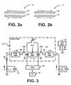
- An MRAM device comprising:an array (10) including a plurality of columns of memory cells (12) and at least one column of reference cells (26);a plurality of bit lines, wherein, for each column, the memory cells (12) of a column are connected to a memory bit line (16), and wherein the reference cells (26) of a column are connected to a reference bit line (28); anda read circuit (20) for sensing resistance states of selected memory cells (12) in the array (10), the read circuit (20) including:a plurality of steering circuits (22), each steering circuit (12) having inputs coupled to multiple memory bit lines (16);a plurality of differential amplifiers (34), each differential amplifier (34) corresponding to a steering circuit (22), each differential amplifier (34) having a sense node (S0) and a reference node (R0);a plurality of first current mode preamplifiers (38), each first current mode preamplifier (38) being coupled between an output of a corresponding steering circuit (22) and the sense node (S0) of a corresponding differential amplifier (34); anda plurality of second current mode preamplifiers (42), each second current mode preamplifier (42) being coupled between the reference node (R0) of a corresponding differential amplifier (34) and a bit line (28) connected to a reference cell column.
- The device of claim 1, wherein the device (8') includes a single column of reference cells (26); and wherein the reference bit line (28) connected to the reference cells (26) of the single column is connected to the reference node (R0) of each differential amplifier (34).
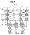
- The device of claim 1, wherein the device (8) includes a plurality of reference cell columns, each reference cell column corresponding to a differential amplifier (34); and wherein the reference bit line (28) connected to the reference cells of a reference cell column is connected to the reference node (R0) of the corresponding differential amplifier (34).
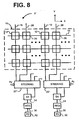
- The device of claim 1, wherein the device (8") includes a plurality of reference cell columns, each reference cell column corresponding to a memory cell column; wherein the memory bit line (16) connected to a memory cell in a memory cell column and the reference bit line (28) connected to a reference cell in a corresponding reference cell column are connected to the same steering circuit (22").
- The device of claim 1, wherein the first and second preamplifiers (38 and 42) are direct-injection charge amplifiers.
- The device of claim 1, wherein the first and second preamplifiers (38 and 42) are current-mirror charge amplifiers.
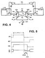
- The device of claim 1, further comprising at least one clock generator (44) for generating an Equalization signal, the Equalization signal being asserted to cause the sense and reference nodes (S0 and R0) of a differential amplifier (34) to be equalized, the asserted Equalization signal also causing at least one differential amplifier (34) to pull its node voltages toward a source voltage, a voltage differential developing across the sense and reference nodes (S0 and R0) of at least one differential amplifier (34) after the Equalization signal has been de-asserted.
- The device of claim 7, wherein each clock generator (44) also generates a Set signal, the Set signal being asserted after the Equalization signal has been de-asserted.
- The device of claim 8, further comprising a plurality of first and second switches (36 and 40), each first switch (36) coupling a corresponding first preamplifier (38) to the sense node (S0) of a corresponding differential amplifier (34), each second switch (40) coupling a corresponding second preamplifier (42) to the reference node (R0) of a corresponding differential amplifier (34); wherein each clock generator (44) also generates an Unload signal, the Unload signal being asserted after the Equalization signal is de-asserted but before the Set signal is asserted, the asserted Unload signal causing the first and second switches (36 and 40) to disconnect their corresponding differential amplifier (34) from their corresponding first and second preamplifiers (38 and 42).
Applications Claiming Priority (2)
| Application Number | Priority Date | Filing Date | Title |
|---|---|---|---|
| US09/498,587 US6185143B1 (en) | 2000-02-04 | 2000-02-04 | Magnetic random access memory (MRAM) device including differential sense amplifiers |
| US498587 | 2000-02-04 |
Publications (3)
| Publication Number | Publication Date |
|---|---|
| EP1126468A2 EP1126468A2 (en) | 2001-08-22 |
| EP1126468A3 EP1126468A3 (en) | 2001-09-19 |
| EP1126468B1 true EP1126468B1 (en) | 2005-12-28 |
Family
ID=23981674
Family Applications (1)
| Application Number | Title | Priority Date | Filing Date |
|---|---|---|---|
| EP00122074A Expired - Lifetime EP1126468B1 (en) | 2000-02-04 | 2000-10-11 | MRAM device including differential sense amplifiers |
Country Status (6)
| Country | Link |
|---|---|
| US (2) | US6185143B1 (en) |
| EP (1) | EP1126468B1 (en) |
| JP (1) | JP4758554B2 (en) |
| CN (1) | CN1319846A (en) |
| DE (1) | DE60025152T2 (en) |
| HK (1) | HK1041362A1 (en) |
Cited By (14)
| Publication number | Priority date | Publication date | Assignee | Title |
|---|---|---|---|---|
| US7652930B2 (en) | 2004-04-01 | 2010-01-26 | Saifun Semiconductors Ltd. | Method, circuit and system for erasing one or more non-volatile memory cells |
| US7668017B2 (en) | 2005-08-17 | 2010-02-23 | Saifun Semiconductors Ltd. | Method of erasing non-volatile memory cells |
| US7675782B2 (en) | 2002-10-29 | 2010-03-09 | Saifun Semiconductors Ltd. | Method, system and circuit for programming a non-volatile memory array |
| US7692961B2 (en) | 2006-02-21 | 2010-04-06 | Saifun Semiconductors Ltd. | Method, circuit and device for disturb-control of programming nonvolatile memory cells by hot-hole injection (HHI) and by channel hot-electron (CHE) injection |
| US7701779B2 (en) | 2006-04-27 | 2010-04-20 | Sajfun Semiconductors Ltd. | Method for programming a reference cell |
| US7738304B2 (en) | 2002-07-10 | 2010-06-15 | Saifun Semiconductors Ltd. | Multiple use memory chip |
| US7743230B2 (en) | 2003-01-31 | 2010-06-22 | Saifun Semiconductors Ltd. | Memory array programming circuit and a method for using the circuit |
| US7760554B2 (en) | 2006-02-21 | 2010-07-20 | Saifun Semiconductors Ltd. | NROM non-volatile memory and mode of operation |
| US7786512B2 (en) | 2005-07-18 | 2010-08-31 | Saifun Semiconductors Ltd. | Dense non-volatile memory array and method of fabrication |
| US7808818B2 (en) | 2006-01-12 | 2010-10-05 | Saifun Semiconductors Ltd. | Secondary injection for NROM |
| US7964459B2 (en) | 2004-10-14 | 2011-06-21 | Spansion Israel Ltd. | Non-volatile memory structure and method of fabrication |
| US8053812B2 (en) | 2005-03-17 | 2011-11-08 | Spansion Israel Ltd | Contact in planar NROM technology |
| US8253452B2 (en) | 2006-02-21 | 2012-08-28 | Spansion Israel Ltd | Circuit and method for powering up an integrated circuit and an integrated circuit utilizing same |
| US8400841B2 (en) | 2005-06-15 | 2013-03-19 | Spansion Israel Ltd. | Device to program adjacent storage cells of different NROM cells |
Families Citing this family (179)
| Publication number | Priority date | Publication date | Assignee | Title |
|---|---|---|---|---|
| US6768165B1 (en) * | 1997-08-01 | 2004-07-27 | Saifun Semiconductors Ltd. | Two bit non-volatile electrically erasable and programmable semiconductor memory cell utilizing asymmetrical charge trapping |
| JP2001273796A (en) * | 2000-03-29 | 2001-10-05 | Nec Microsystems Ltd | Sense amplifier circuit |
| US6317376B1 (en) * | 2000-06-20 | 2001-11-13 | Hewlett-Packard Company | Reference signal generation for magnetic random access memory devices |
| DE10032271C2 (en) * | 2000-07-03 | 2002-08-01 | Infineon Technologies Ag | MRAM configuration |
| US6396733B1 (en) * | 2000-07-17 | 2002-05-28 | Micron Technology, Inc. | Magneto-resistive memory having sense amplifier with offset control |
| US6538921B2 (en) | 2000-08-17 | 2003-03-25 | Nve Corporation | Circuit selection of magnetic memory cells and related cell structures |
| TW564418B (en) * | 2000-12-29 | 2003-12-01 | Amic Technology Taiwan Inc | Sensing circuit for magnetic memory unit |
| US6426907B1 (en) | 2001-01-24 | 2002-07-30 | Infineon Technologies North America Corp. | Reference for MRAM cell |
| US6356477B1 (en) * | 2001-01-29 | 2002-03-12 | Hewlett Packard Company | Cross point memory array including shared devices for blocking sneak path currents |
| US6567297B2 (en) * | 2001-02-01 | 2003-05-20 | Micron Technology, Inc. | Method and apparatus for sensing resistance values of memory cells |
| US6687178B1 (en) | 2001-02-23 | 2004-02-03 | Western Digital (Fremont), Inc. | Temperature dependent write current source for magnetic tunnel junction MRAM |
| US6803615B1 (en) | 2001-02-23 | 2004-10-12 | Western Digital (Fremont), Inc. | Magnetic tunnel junction MRAM with improved stability |
| US6721203B1 (en) | 2001-02-23 | 2004-04-13 | Western Digital (Fremont), Inc. | Designs of reference cells for magnetic tunnel junction (MTJ) MRAM |
| US6392923B1 (en) * | 2001-02-27 | 2002-05-21 | Motorola, Inc. | Magnetoresistive midpoint generator and method |
| US6504753B1 (en) * | 2001-03-21 | 2003-01-07 | Matrix Semiconductor, Inc. | Method and apparatus for discharging memory array lines |
| US6522594B1 (en) * | 2001-03-21 | 2003-02-18 | Matrix Semiconductor, Inc. | Memory array incorporating noise detection line |
| US7177181B1 (en) * | 2001-03-21 | 2007-02-13 | Sandisk 3D Llc | Current sensing method and apparatus particularly useful for a memory array of cells having diode-like characteristics |
| JP2002299575A (en) * | 2001-03-29 | 2002-10-11 | Toshiba Corp | Semiconductor memory |
| US6584017B2 (en) | 2001-04-05 | 2003-06-24 | Saifun Semiconductors Ltd. | Method for programming a reference cell |
| IL148959A (en) * | 2001-04-05 | 2006-09-05 | Saifun Semiconductors Ltd | Architecture and scheme for a non-strobed read sequence |
| US6535434B2 (en) * | 2001-04-05 | 2003-03-18 | Saifun Semiconductors Ltd. | Architecture and scheme for a non-strobed read sequence |
| JP5019681B2 (en) * | 2001-04-26 | 2012-09-05 | ルネサスエレクトロニクス株式会社 | Thin film magnetic memory device |
| US6744086B2 (en) | 2001-05-15 | 2004-06-01 | Nve Corporation | Current switched magnetoresistive memory cell |
| JP4731041B2 (en) * | 2001-05-16 | 2011-07-20 | ルネサスエレクトロニクス株式会社 | Thin film magnetic memory device |
| US6930516B2 (en) * | 2001-05-30 | 2005-08-16 | Agere Systems Inc. | Comparator circuits having non-complementary input structures |
| JP2003016777A (en) * | 2001-06-28 | 2003-01-17 | Mitsubishi Electric Corp | Thin film magnetic storage device |
| US6515896B1 (en) | 2001-07-24 | 2003-02-04 | Hewlett-Packard Company | Memory device with short read time |
| US6803616B2 (en) * | 2002-06-17 | 2004-10-12 | Hewlett-Packard Development Company, L.P. | Magnetic memory element having controlled nucleation site in data layer |
| US6829158B2 (en) * | 2001-08-22 | 2004-12-07 | Motorola, Inc. | Magnetoresistive level generator and method |
| US6445612B1 (en) * | 2001-08-27 | 2002-09-03 | Motorola, Inc. | MRAM with midpoint generator reference and method for readout |
| US6510080B1 (en) * | 2001-08-28 | 2003-01-21 | Micron Technology Inc. | Three terminal magnetic random access memory |
| US6577525B2 (en) * | 2001-08-28 | 2003-06-10 | Micron Technology, Inc. | Sensing method and apparatus for resistance memory device |
| US6385079B1 (en) * | 2001-08-31 | 2002-05-07 | Hewlett-Packard Company | Methods and structure for maximizing signal to noise ratio in resistive array |
| US6496051B1 (en) | 2001-09-06 | 2002-12-17 | Sharp Laboratories Of America, Inc. | Output sense amplifier for a multibit memory cell |
| US6501697B1 (en) | 2001-10-11 | 2002-12-31 | Hewlett-Packard Company | High density memory sense amplifier |
| US6545906B1 (en) * | 2001-10-16 | 2003-04-08 | Motorola, Inc. | Method of writing to scalable magnetoresistance random access memory element |
| EP1304701A1 (en) * | 2001-10-18 | 2003-04-23 | STMicroelectronics S.r.l. | Sensing circuit for ferroelectric non-volatile memories |
| US6456524B1 (en) * | 2001-10-31 | 2002-09-24 | Hewlett-Packard Company | Hybrid resistive cross point memory cell arrays and methods of making the same |
| JP2003151262A (en) * | 2001-11-15 | 2003-05-23 | Toshiba Corp | Magnetic random access memory |
| US7098107B2 (en) * | 2001-11-19 | 2006-08-29 | Saifun Semiconductor Ltd. | Protective layer in memory device and method therefor |
| JP4052829B2 (en) * | 2001-12-12 | 2008-02-27 | 株式会社ルネサステクノロジ | Thin film magnetic memory device |
| EP1324344B1 (en) * | 2001-12-28 | 2007-04-04 | STMicroelectronics S.r.l. | Sense amplifier structure for multilevel non-volatile memory devices and corresponding reading method |
| US6650562B2 (en) * | 2002-01-23 | 2003-11-18 | Hewlett-Packard Development Company, L.P. | System and method for determining the logic state of a memory cell in a magnetic tunnel junction memory device |
| JP4046513B2 (en) * | 2002-01-30 | 2008-02-13 | 株式会社ルネサステクノロジ | Semiconductor integrated circuit |
| US6700818B2 (en) * | 2002-01-31 | 2004-03-02 | Saifun Semiconductors Ltd. | Method for operating a memory device |
| WO2003067598A2 (en) * | 2002-02-06 | 2003-08-14 | Koninklijke Philips Electronics N.V. | Reading circuit for reading a memory cell |
| US6678189B2 (en) * | 2002-02-25 | 2004-01-13 | Hewlett-Packard Development Company, L.P. | Method and system for performing equipotential sensing across a memory array to eliminate leakage currents |
| US6885573B2 (en) | 2002-03-15 | 2005-04-26 | Hewlett-Packard Development Company, L.P. | Diode for use in MRAM devices and method of manufacture |
| US6593608B1 (en) | 2002-03-15 | 2003-07-15 | Hewlett-Packard Development Company, L.P. | Magneto resistive storage device having double tunnel junction |
| KR100464536B1 (en) * | 2002-03-22 | 2005-01-03 | 주식회사 하이닉스반도체 | Magnetoresistive RAM |
| US6625055B1 (en) | 2002-04-09 | 2003-09-23 | Hewlett-Packard Development Company, L.P. | Multiple logical bits per memory cell in a memory device |
| JP4071531B2 (en) * | 2002-04-23 | 2008-04-02 | 株式会社ルネサステクノロジ | Thin film magnetic memory device |
| US6597598B1 (en) | 2002-04-30 | 2003-07-22 | Hewlett-Packard Development Company, L.P. | Resistive cross point memory arrays having a charge injection differential sense amplifier |
| US6574129B1 (en) * | 2002-04-30 | 2003-06-03 | Hewlett-Packard Development Company, L.P. | Resistive cross point memory cell arrays having a cross-couple latch sense amplifier |
| US6724652B2 (en) * | 2002-05-02 | 2004-04-20 | Micron Technology, Inc. | Low remanence flux concentrator for MRAM devices |
| US7023243B2 (en) * | 2002-05-08 | 2006-04-04 | University Of Southern California | Current source evaluation sense-amplifier |
| GB0210719D0 (en) * | 2002-05-10 | 2002-06-19 | Koninkl Philips Electronics Nv | Memories and memory circuits |
| US7042749B2 (en) | 2002-05-16 | 2006-05-09 | Micron Technology, Inc. | Stacked 1T-nmemory cell structure |
| AU2003243244A1 (en) * | 2002-05-16 | 2003-12-02 | Micron Technology, Inc. | STACKED 1T-nMEMORY CELL STRUCTURE |
| US6940748B2 (en) * | 2002-05-16 | 2005-09-06 | Micron Technology, Inc. | Stacked 1T-nMTJ MRAM structure |
| US20030218905A1 (en) * | 2002-05-22 | 2003-11-27 | Perner Frederick A. | Equi-potential sensing magnetic random access memory (MRAM) with series diodes |
| JP4208498B2 (en) * | 2002-06-21 | 2009-01-14 | 株式会社ルネサステクノロジ | Thin film magnetic memory device |
| US6760266B2 (en) * | 2002-06-28 | 2004-07-06 | Freescale Semiconductor, Inc. | Sense amplifier and method for performing a read operation in a MRAM |
| US6693824B2 (en) | 2002-06-28 | 2004-02-17 | Motorola, Inc. | Circuit and method of writing a toggle memory |
| US6744663B2 (en) | 2002-06-28 | 2004-06-01 | Motorola, Inc. | Circuit and method for reading a toggle memory cell |
| US6903964B2 (en) * | 2002-06-28 | 2005-06-07 | Freescale Semiconductor, Inc. | MRAM architecture with electrically isolated read and write circuitry |
| JP3821066B2 (en) | 2002-07-04 | 2006-09-13 | 日本電気株式会社 | Magnetic random access memory |
| US7095646B2 (en) * | 2002-07-17 | 2006-08-22 | Freescale Semiconductor, Inc. | Multi-state magnetoresistance random access cell with improved memory storage density |
| US6882553B2 (en) | 2002-08-08 | 2005-04-19 | Micron Technology Inc. | Stacked columnar resistive memory structure and its method of formation and operation |
| US7152800B2 (en) * | 2002-08-22 | 2006-12-26 | Texas Instruments Incorporated | Preamplifier system having programmable resistance |
| US6791865B2 (en) * | 2002-09-03 | 2004-09-14 | Hewlett-Packard Development Company, L.P. | Memory device capable of calibration and calibration methods therefor |
| JP4679036B2 (en) * | 2002-09-12 | 2011-04-27 | ルネサスエレクトロニクス株式会社 | Storage device |
| US6674679B1 (en) * | 2002-10-01 | 2004-01-06 | Hewlett-Packard Development Company, L.P. | Adjustable current mode differential amplifier for multiple bias point sensing of MRAM having equi-potential isolation |
| US6834017B2 (en) * | 2002-10-03 | 2004-12-21 | Hewlett-Packard Development Company, L.P. | Error detection system for an information storage device |
| US6963505B2 (en) | 2002-10-29 | 2005-11-08 | Aifun Semiconductors Ltd. | Method circuit and system for determining a reference voltage |
| US6992932B2 (en) | 2002-10-29 | 2006-01-31 | Saifun Semiconductors Ltd | Method circuit and system for read error detection in a non-volatile memory array |
| US6700814B1 (en) | 2002-10-30 | 2004-03-02 | Motorola, Inc. | Sense amplifier bias circuit for a memory having at least two distinct resistance states |
| US6944052B2 (en) * | 2002-11-26 | 2005-09-13 | Freescale Semiconductor, Inc. | Magnetoresistive random access memory (MRAM) cell having a diode with asymmetrical characteristics |
| US6738303B1 (en) * | 2002-11-27 | 2004-05-18 | Motorola, Inc. | Technique for sensing the state of a magneto-resistive random access memory |
| EP1568038B1 (en) * | 2002-11-28 | 2011-01-26 | Nxp B.V. | A method and device to detect the likely onset of thermal relaxation in magnetic data storage devices |
| US6806127B2 (en) * | 2002-12-03 | 2004-10-19 | Freescale Semiconductor, Inc. | Method and structure for contacting an overlying electrode for a magnetoelectronics element |
| JP3766380B2 (en) * | 2002-12-25 | 2006-04-12 | 株式会社東芝 | Magnetic random access memory and data read method of the magnetic random access memory |
| US6888743B2 (en) * | 2002-12-27 | 2005-05-03 | Freescale Semiconductor, Inc. | MRAM architecture |
| US6909631B2 (en) * | 2003-10-02 | 2005-06-21 | Freescale Semiconductor, Inc. | MRAM and methods for reading the MRAM |
| US6836443B2 (en) * | 2003-01-14 | 2004-12-28 | Tower Semiconductor Ltd. | Apparatus and method of high speed current sensing for low voltage operation |
| US6967896B2 (en) * | 2003-01-30 | 2005-11-22 | Saifun Semiconductors Ltd | Address scramble |
| US7002228B2 (en) * | 2003-02-18 | 2006-02-21 | Micron Technology, Inc. | Diffusion barrier for improving the thermal stability of MRAM devices |
| US6868025B2 (en) * | 2003-03-10 | 2005-03-15 | Sharp Laboratories Of America, Inc. | Temperature compensated RRAM circuit |
| US6838721B2 (en) * | 2003-04-25 | 2005-01-04 | Freescale Semiconductor, Inc. | Integrated circuit with a transitor over an interconnect layer |
| US7142464B2 (en) * | 2003-04-29 | 2006-11-28 | Saifun Semiconductors Ltd. | Apparatus and methods for multi-level sensing in a memory array |
| US6816403B1 (en) | 2003-05-14 | 2004-11-09 | International Business Machines Corporation | Capacitively coupled sensing apparatus and method for cross point magnetic random access memory devices |
| US7042783B2 (en) * | 2003-06-18 | 2006-05-09 | Hewlett-Packard Development Company, L.P. | Magnetic memory |
| US6956763B2 (en) * | 2003-06-27 | 2005-10-18 | Freescale Semiconductor, Inc. | MRAM element and methods for writing the MRAM element |
| US6826086B1 (en) | 2003-08-05 | 2004-11-30 | Hewlett-Packard Development Company, L.P. | Method, apparatus and system for erasing and writing a magnetic random access memory |
| US6751147B1 (en) | 2003-08-05 | 2004-06-15 | Hewlett-Packard Development Company, L.P. | Method for adaptively writing a magnetic random access memory |
| US7240275B2 (en) * | 2003-08-05 | 2007-07-03 | Hewlett-Packard Development Company, L.P. | Logical data block, magnetic random access memory, memory module, computer system and method |
| US6967366B2 (en) * | 2003-08-25 | 2005-11-22 | Freescale Semiconductor, Inc. | Magnetoresistive random access memory with reduced switching field variation |
| GB0320339D0 (en) * | 2003-08-29 | 2003-10-01 | Isis Innovation | Resistance array reader |
| US7123532B2 (en) * | 2003-09-16 | 2006-10-17 | Saifun Semiconductors Ltd. | Operating array cells with matched reference cells |
| US6985383B2 (en) * | 2003-10-20 | 2006-01-10 | Taiwan Semiconductor Manufacturing Company, Ltd. | Reference generator for multilevel nonlinear resistivity memory storage elements |
| US6847544B1 (en) | 2003-10-20 | 2005-01-25 | Hewlett-Packard Development Company, L.P. | Magnetic memory which detects changes between first and second resistive states of memory cell |
| US6990030B2 (en) * | 2003-10-21 | 2006-01-24 | Hewlett-Packard Development Company, L.P. | Magnetic memory having a calibration system |
| US7286378B2 (en) * | 2003-11-04 | 2007-10-23 | Micron Technology, Inc. | Serial transistor-cell array architecture |
| US7064970B2 (en) * | 2003-11-04 | 2006-06-20 | Micron Technology, Inc. | Serial transistor-cell array architecture |
| WO2005050712A2 (en) * | 2003-11-18 | 2005-06-02 | Halliburton Energy Services, Inc. | High-temperature memory systems |
| US7099179B2 (en) * | 2003-12-22 | 2006-08-29 | Unity Semiconductor Corporation | Conductive memory array having page mode and burst mode write capability |
| US7095644B2 (en) * | 2003-12-22 | 2006-08-22 | Unity Semiconductor Corporation | Conductive memory array having page mode and burst mode read capability |
| US7072209B2 (en) * | 2003-12-29 | 2006-07-04 | Micron Technology, Inc. | Magnetic memory having synthetic antiferromagnetic pinned layer |
| US7251159B2 (en) * | 2004-01-09 | 2007-07-31 | Broadcom Corporation | Data encoding approach for implementing robust non-volatile memories |
| JP3845096B2 (en) * | 2004-02-12 | 2006-11-15 | 株式会社東芝 | Magnetic storage |
| US7079438B2 (en) * | 2004-02-17 | 2006-07-18 | Hewlett-Packard Development Company, L.P. | Controlled temperature, thermal-assisted magnetic memory device |
| DE102004015928A1 (en) * | 2004-03-31 | 2005-10-27 | Infineon Technologies Ag | Write / erase method for resistively switching memory devices |
| US7027323B2 (en) * | 2004-04-02 | 2006-04-11 | Hewlett-Packard Development Company, L.P. | Storage device having parallel connected memory cells that include magnetoresistive elements |
| US7755938B2 (en) * | 2004-04-19 | 2010-07-13 | Saifun Semiconductors Ltd. | Method for reading a memory array with neighbor effect cancellation |
| US7362549B2 (en) * | 2004-05-19 | 2008-04-22 | Seagate Technology Llc | Storage device having first and second magnetic elements that interact magnetically to indicate a storage state |
| US7075817B2 (en) * | 2004-07-20 | 2006-07-11 | Unity Semiconductor Corporation | Two terminal memory array having reference cells |
| US7203112B2 (en) * | 2004-08-05 | 2007-04-10 | Taiwan Semiconductor Manufacturing Co., Ltd. | Multiple stage method and system for sensing outputs from memory cells |
| US7095655B2 (en) * | 2004-08-12 | 2006-08-22 | Saifun Semiconductors Ltd. | Dynamic matching of signal path and reference path for sensing |
| US8578063B2 (en) * | 2004-08-20 | 2013-11-05 | Mitsubishi Kagaku Media Co., Ltd. | Self-labeling digital storage unit |
| US7130235B2 (en) * | 2004-09-03 | 2006-10-31 | Hewlett-Packard Development Company, L.P. | Method and apparatus for a sense amplifier |
| US7038959B2 (en) * | 2004-09-17 | 2006-05-02 | Freescale Semiconductor, Inc. | MRAM sense amplifier having a precharge circuit and method for sensing |
| US20060068551A1 (en) * | 2004-09-27 | 2006-03-30 | Saifun Semiconductors, Ltd. | Method for embedding NROM |
| JP4660163B2 (en) * | 2004-10-29 | 2011-03-30 | 東芝メモリシステムズ株式会社 | Semiconductor memory device |
| US7129098B2 (en) * | 2004-11-24 | 2006-10-31 | Freescale Semiconductor, Inc. | Reduced power magnetoresistive random access memory elements |
| US20060146624A1 (en) * | 2004-12-02 | 2006-07-06 | Saifun Semiconductors, Ltd. | Current folding sense amplifier |
| US7257025B2 (en) * | 2004-12-09 | 2007-08-14 | Saifun Semiconductors Ltd | Method for reading non-volatile memory cells |
| CN1838323A (en) * | 2005-01-19 | 2006-09-27 | 赛芬半导体有限公司 | Methods for preventing fixed pattern programming |
| US20060230273A1 (en) * | 2005-04-08 | 2006-10-12 | Eastman Kodak Company | Hidden MIRC printing for security |
| US20070141788A1 (en) * | 2005-05-25 | 2007-06-21 | Ilan Bloom | Method for embedding non-volatile memory with logic circuitry |
| US7184313B2 (en) * | 2005-06-17 | 2007-02-27 | Saifun Semiconductors Ltd. | Method circuit and system for compensating for temperature induced margin loss in non-volatile memory cells |
| US20070036007A1 (en) * | 2005-08-09 | 2007-02-15 | Saifun Semiconductors, Ltd. | Sticky bit buffer |
| US7272035B1 (en) * | 2005-08-31 | 2007-09-18 | Grandis, Inc. | Current driven switching of magnetic storage cells utilizing spin transfer and magnetic memories using such cells |
| US7272034B1 (en) * | 2005-08-31 | 2007-09-18 | Grandis, Inc. | Current driven switching of magnetic storage cells utilizing spin transfer and magnetic memories using such cells |
| US20070096199A1 (en) * | 2005-09-08 | 2007-05-03 | Eli Lusky | Method of manufacturing symmetric arrays |
| JPWO2007043358A1 (en) * | 2005-10-07 | 2009-04-16 | コニカミノルタオプト株式会社 | Method for producing cellulose ester film, cellulose ester film, polarizing plate and liquid crystal display device |
| US7426133B2 (en) * | 2005-10-24 | 2008-09-16 | Honeywell International, Inc. | Complementary giant magneto-resistive memory with full-turn word line |
| US20070120180A1 (en) * | 2005-11-25 | 2007-05-31 | Boaz Eitan | Transition areas for dense memory arrays |
| US7352627B2 (en) * | 2006-01-03 | 2008-04-01 | Saifon Semiconductors Ltd. | Method, system, and circuit for operating a non-volatile memory array |
| US20070173017A1 (en) * | 2006-01-20 | 2007-07-26 | Saifun Semiconductors, Ltd. | Advanced non-volatile memory array and method of fabrication thereof |
| US7881138B2 (en) * | 2006-07-10 | 2011-02-01 | Freescale Semiconductor, Inc. | Memory circuit with sense amplifier |
| US7561472B2 (en) | 2006-09-11 | 2009-07-14 | Micron Technology, Inc. | NAND architecture memory with voltage sensing |
| US7605579B2 (en) * | 2006-09-18 | 2009-10-20 | Saifun Semiconductors Ltd. | Measuring and controlling current consumption and output current of charge pumps |
| KR100866623B1 (en) * | 2006-10-16 | 2008-11-03 | 삼성전자주식회사 | Sense Amplifying Circuit and Nonvolatile Memory Device capable of operating with low power supply |
| US7379364B2 (en) * | 2006-10-19 | 2008-05-27 | Unity Semiconductor Corporation | Sensing a signal in a two-terminal memory array having leakage current |
| US7372753B1 (en) * | 2006-10-19 | 2008-05-13 | Unity Semiconductor Corporation | Two-cycle sensing in a two-terminal memory array having leakage current |
| US7567462B2 (en) * | 2006-11-16 | 2009-07-28 | Micron Technology, Inc. | Method and system for selectively limiting peak power consumption during programming or erase of non-volatile memory devices |
| US7453740B2 (en) * | 2007-01-19 | 2008-11-18 | International Business Machines Corporation | Method and apparatus for initializing reference cells of a toggle switched MRAM device |
| US20080239599A1 (en) * | 2007-04-01 | 2008-10-02 | Yehuda Yizraeli | Clamping Voltage Events Such As ESD |
| US9135962B2 (en) * | 2007-06-15 | 2015-09-15 | Micron Technology, Inc. | Comparators for delta-sigma modulators |
| US7813166B2 (en) * | 2008-06-30 | 2010-10-12 | Qualcomm Incorporated | Controlled value reference signal of resistance based memory circuit |
| JP2010055719A (en) * | 2008-08-29 | 2010-03-11 | Toshiba Corp | Resistance change memory device |
| US7936590B2 (en) * | 2008-12-08 | 2011-05-03 | Qualcomm Incorporated | Digitally-controllable delay for sense amplifier |
| US8208330B2 (en) | 2009-07-24 | 2012-06-26 | Macronix International Co., Ltd. | Sense amplifier with shielding circuit |
| CN103222002B (en) * | 2010-11-19 | 2018-04-24 | 慧与发展有限责任合伙企业 | For reading the circuit and method of the resistor switching device in array |
| US8611132B2 (en) * | 2011-04-29 | 2013-12-17 | Qualcomm Incorporated | Self-body biasing sensing circuit for resistance-based memories |
| WO2013032424A1 (en) * | 2011-08-26 | 2013-03-07 | Hewlett-Packard Development Company, L.P. | Circuit and method for reading a resistive switching device in an array |
| KR102049306B1 (en) | 2011-12-12 | 2019-11-27 | 삼성전자주식회사 | Memory device, method of performing read or write operation and memory system including the same |
| US8570819B2 (en) * | 2012-03-09 | 2013-10-29 | Actel Corporation | Non-volatile memory array architecture optimized for hi-reliability and commercial markets |
| US8912517B2 (en) | 2012-09-24 | 2014-12-16 | Adesto Technologies Corporation | Resistive switching memory |
| KR102005226B1 (en) * | 2012-10-29 | 2019-07-30 | 삼성전자 주식회사 | Nonvolatile memory device using variable resistive element and driving method thereof |
| KR102023358B1 (en) * | 2012-10-29 | 2019-09-20 | 삼성전자 주식회사 | Nonvolatile memory device using variable resistive element and driving method thereof |
| US9058875B2 (en) | 2012-12-17 | 2015-06-16 | Micron Technology, Inc. | Resistive memory sensing |
| US9384792B2 (en) | 2014-04-09 | 2016-07-05 | Globalfoundries Inc. | Offset-cancelling self-reference STT-MRAM sense amplifier |
| US9472257B2 (en) * | 2014-05-15 | 2016-10-18 | Qualcomm Incorporated | Hybrid magnetoresistive read only memory (MRAM) cache mixing single-ended and differential sensing |
| US9373383B2 (en) | 2014-09-12 | 2016-06-21 | International Business Machines Corporation | STT-MRAM sensing technique |
| KR20170063649A (en) | 2014-09-30 | 2017-06-08 | 휴렛 팩커드 엔터프라이즈 디벨롭먼트 엘피 | Crosspoint array decoder |
| US10008264B2 (en) | 2014-10-23 | 2018-06-26 | Hewlett Packard Enterprise Development Lp | Memristive cross-bar array for determining a dot product |
| CN105741864B (en) * | 2016-02-03 | 2018-08-21 | 上海磁宇信息科技有限公司 | A kind of sense amplifier and MRAM chip |
| CN105761745B (en) * | 2016-02-03 | 2018-05-22 | 上海磁宇信息科技有限公司 | A kind of sense amplifier and MRAM chip |
| KR102514045B1 (en) | 2016-04-21 | 2023-03-24 | 삼성전자주식회사 | Resistive Memory device and Memory system including thereof |
| JP2018147534A (en) | 2017-03-03 | 2018-09-20 | ソニーセミコンダクタソリューションズ株式会社 | Sense amplifier, semiconductor memory device, information processor and reading out method |
| JP2018163728A (en) * | 2017-03-24 | 2018-10-18 | 東芝メモリ株式会社 | Memory device and control method of memory device |
| JP2019057348A (en) * | 2017-09-21 | 2019-04-11 | 東芝メモリ株式会社 | Memory device |
| US11222259B2 (en) | 2017-12-13 | 2022-01-11 | International Business Machines Corporation | Counter based resistive processing unit for programmable and reconfigurable artificial-neural-networks |
| CN108133725B (en) * | 2017-12-19 | 2021-06-29 | 上海磁宇信息科技有限公司 | MRAM readout circuit using low voltage pulse |
| US10381074B1 (en) | 2018-04-10 | 2019-08-13 | International Business Machines Corporation | Differential weight reading of an analog memory element in crosspoint array utilizing current subtraction transistors |
| US10726895B1 (en) | 2019-01-07 | 2020-07-28 | International Business Machines Corporation | Circuit methodology for differential weight reading in resistive processing unit devices |
| JP2020135913A (en) * | 2019-02-25 | 2020-08-31 | キオクシア株式会社 | Semiconductor storage device |
| CN111540396B (en) * | 2020-04-27 | 2022-04-01 | 中国科学院微电子研究所 | MRAM reading device and method for overcoming process floating of memory cell |
Family Cites Families (9)
| Publication number | Priority date | Publication date | Assignee | Title |
|---|---|---|---|---|
| US4633443A (en) * | 1984-07-09 | 1986-12-30 | Texas Instruments Incorporated | Dynamic read/write memory circuits with equal-sized dummy and storage capacitors |
| US5898612A (en) * | 1997-05-22 | 1999-04-27 | Motorola, Inc. | Magnetic memory cell with increased GMR ratio |
| US5831920A (en) * | 1997-10-14 | 1998-11-03 | Motorola, Inc. | GMR device having a sense amplifier protected by a circuit for dissipating electric charges |
| US5982658A (en) * | 1997-10-31 | 1999-11-09 | Honeywell Inc. | MRAM design to reduce dissimilar nearest neighbor effects |
| US6111781A (en) * | 1998-08-03 | 2000-08-29 | Motorola, Inc. | Magnetic random access memory array divided into a plurality of memory banks |
| DE19853447A1 (en) * | 1998-11-19 | 2000-05-25 | Siemens Ag | Magnetic storage |
| US6055178A (en) * | 1998-12-18 | 2000-04-25 | Motorola, Inc. | Magnetic random access memory with a reference memory array |
| DE19914489C1 (en) * | 1999-03-30 | 2000-06-08 | Siemens Ag | Memory cell condition evaluation device for magnetoresistive memory |
| US6128239A (en) * | 1999-10-29 | 2000-10-03 | Hewlett-Packard | MRAM device including analog sense amplifiers |
-
2000
- 2000-02-04 US US09/498,587 patent/US6185143B1/en not_active Expired - Lifetime
- 2000-10-11 DE DE60025152T patent/DE60025152T2/en not_active Expired - Lifetime
- 2000-10-11 EP EP00122074A patent/EP1126468B1/en not_active Expired - Lifetime
- 2000-11-06 CN CN00133877A patent/CN1319846A/en active Pending
- 2000-12-19 US US09/745,103 patent/US6256247B1/en not_active Expired - Lifetime
-
2001
- 2001-02-05 JP JP2001028596A patent/JP4758554B2/en not_active Expired - Fee Related
-
2002
- 2002-04-08 HK HK02102605.1A patent/HK1041362A1/en unknown
Cited By (14)
| Publication number | Priority date | Publication date | Assignee | Title |
|---|---|---|---|---|
| US7738304B2 (en) | 2002-07-10 | 2010-06-15 | Saifun Semiconductors Ltd. | Multiple use memory chip |
| US7675782B2 (en) | 2002-10-29 | 2010-03-09 | Saifun Semiconductors Ltd. | Method, system and circuit for programming a non-volatile memory array |
| US7743230B2 (en) | 2003-01-31 | 2010-06-22 | Saifun Semiconductors Ltd. | Memory array programming circuit and a method for using the circuit |
| US7652930B2 (en) | 2004-04-01 | 2010-01-26 | Saifun Semiconductors Ltd. | Method, circuit and system for erasing one or more non-volatile memory cells |
| US7964459B2 (en) | 2004-10-14 | 2011-06-21 | Spansion Israel Ltd. | Non-volatile memory structure and method of fabrication |
| US8053812B2 (en) | 2005-03-17 | 2011-11-08 | Spansion Israel Ltd | Contact in planar NROM technology |
| US8400841B2 (en) | 2005-06-15 | 2013-03-19 | Spansion Israel Ltd. | Device to program adjacent storage cells of different NROM cells |
| US7786512B2 (en) | 2005-07-18 | 2010-08-31 | Saifun Semiconductors Ltd. | Dense non-volatile memory array and method of fabrication |
| US7668017B2 (en) | 2005-08-17 | 2010-02-23 | Saifun Semiconductors Ltd. | Method of erasing non-volatile memory cells |
| US7808818B2 (en) | 2006-01-12 | 2010-10-05 | Saifun Semiconductors Ltd. | Secondary injection for NROM |
| US7760554B2 (en) | 2006-02-21 | 2010-07-20 | Saifun Semiconductors Ltd. | NROM non-volatile memory and mode of operation |
| US8253452B2 (en) | 2006-02-21 | 2012-08-28 | Spansion Israel Ltd | Circuit and method for powering up an integrated circuit and an integrated circuit utilizing same |
| US7692961B2 (en) | 2006-02-21 | 2010-04-06 | Saifun Semiconductors Ltd. | Method, circuit and device for disturb-control of programming nonvolatile memory cells by hot-hole injection (HHI) and by channel hot-electron (CHE) injection |
| US7701779B2 (en) | 2006-04-27 | 2010-04-20 | Sajfun Semiconductors Ltd. | Method for programming a reference cell |
Also Published As
| Publication number | Publication date |
|---|---|
| JP2001273756A (en) | 2001-10-05 |
| DE60025152T2 (en) | 2006-08-03 |
| JP4758554B2 (en) | 2011-08-31 |
| US6185143B1 (en) | 2001-02-06 |
| EP1126468A3 (en) | 2001-09-19 |
| CN1319846A (en) | 2001-10-31 |
| US6256247B1 (en) | 2001-07-03 |
| US20010012228A1 (en) | 2001-08-09 |
| HK1041362A1 (en) | 2002-07-05 |
| EP1126468A2 (en) | 2001-08-22 |
| DE60025152D1 (en) | 2006-02-02 |
Similar Documents
| Publication | Publication Date | Title |
|---|---|---|
| EP1126468B1 (en) | MRAM device including differential sense amplifiers | |
| US6128239A (en) | MRAM device including analog sense amplifiers | |
| US6259644B1 (en) | Equipotential sense methods for resistive cross point memory cell arrays | |
| US7277319B2 (en) | System and method for reading a memory cell | |
| JP4113033B2 (en) | Resistive crosspoint memory array with charge injection differential sense amplifier | |
| US6574129B1 (en) | Resistive cross point memory cell arrays having a cross-couple latch sense amplifier | |
| JP4046513B2 (en) | Semiconductor integrated circuit | |
| KR100528855B1 (en) | Thin film magnetic memory device reducing a charging time of a data line in a data read operation | |
| KR100522629B1 (en) | Thin film magnetic memory device conducting read operation by a self-reference method | |
| JP2003208784A (en) | Nonvolatile magnetic storage device | |
| JP2002008367A (en) | Magnetic random access memory | |
| KR101136038B1 (en) | Memory cell strings | |
| US6836422B1 (en) | System and method for reading a memory cell | |
| US20070097733A1 (en) | Controllably connectable strings of MRAM cells | |
| JP4067897B2 (en) | Memory device with reduced read time | |
| JP2008084533A (en) | Thin magnetic film storage device | |
| US6865108B2 (en) | Memory cell strings in a resistive cross point memory cell array |
Legal Events
| Date | Code | Title | Description |
|---|---|---|---|
| PUAI | Public reference made under article 153(3) epc to a published international application that has entered the european phase |
Free format text: ORIGINAL CODE: 0009012 |
|
| PUAL | Search report despatched |
Free format text: ORIGINAL CODE: 0009013 |
|
| AK | Designated contracting states |
Kind code of ref document: A2 Designated state(s): AT BE CH CY DE DK ES FI FR GB GR IE IT LI LU MC NL PT SE Kind code of ref document: A2 Designated state(s): DE FR GB |
|
| AX | Request for extension of the european patent |
Free format text: AL;LT;LV;MK;RO;SI |
|
| AK | Designated contracting states |
Kind code of ref document: A3 Designated state(s): AT BE CH CY DE DK ES FI FR GB GR IE IT LI LU MC NL PT SE |
|
| AX | Request for extension of the european patent |
Free format text: AL;LT;LV;MK;RO;SI |
|
| 17P | Request for examination filed |
Effective date: 20020204 |
|
| AKX | Designation fees paid |
Free format text: DE FR GB |
|
| 17Q | First examination report despatched |
Effective date: 20041001 |
|
| GRAP | Despatch of communication of intention to grant a patent |
Free format text: ORIGINAL CODE: EPIDOSNIGR1 |
|
| GRAS | Grant fee paid |
Free format text: ORIGINAL CODE: EPIDOSNIGR3 |
|
| GRAA | (expected) grant |
Free format text: ORIGINAL CODE: 0009210 |
|
| AK | Designated contracting states |
Kind code of ref document: B1 Designated state(s): DE FR GB |
|
| REG | Reference to a national code |
Ref country code: GB Ref legal event code: FG4D |
|
| REF | Corresponds to: |
Ref document number: 60025152 Country of ref document: DE Date of ref document: 20060202 Kind code of ref document: P |
|
| PLBE | No opposition filed within time limit |
Free format text: ORIGINAL CODE: 0009261 |
|
| STAA | Information on the status of an ep patent application or granted ep patent |
Free format text: STATUS: NO OPPOSITION FILED WITHIN TIME LIMIT |
|
| 26N | No opposition filed |
Effective date: 20060929 |
|
| REG | Reference to a national code |
Ref country code: GB Ref legal event code: 732E |
|
| PG25 | Lapsed in a contracting state [announced via postgrant information from national office to epo] |
Ref country code: FR Free format text: LAPSE BECAUSE OF FAILURE TO SUBMIT A TRANSLATION OF THE DESCRIPTION OR TO PAY THE FEE WITHIN THE PRESCRIBED TIME-LIMIT Effective date: 20070216 |
|
| PGFP | Annual fee paid to national office [announced via postgrant information from national office to epo] |
Ref country code: FR Payment date: 20061017 Year of fee payment: 7 |
|
| PG25 | Lapsed in a contracting state [announced via postgrant information from national office to epo] |
Ref country code: FR Free format text: LAPSE BECAUSE OF FAILURE TO SUBMIT A TRANSLATION OF THE DESCRIPTION OR TO PAY THE FEE WITHIN THE PRESCRIBED TIME-LIMIT Effective date: 20051228 |
|
| PGFP | Annual fee paid to national office [announced via postgrant information from national office to epo] |
Ref country code: GB Payment date: 20190923 Year of fee payment: 20 |
|
| PGFP | Annual fee paid to national office [announced via postgrant information from national office to epo] |
Ref country code: DE Payment date: 20190918 Year of fee payment: 20 |
|
| REG | Reference to a national code |
Ref country code: DE Ref legal event code: R071 Ref document number: 60025152 Country of ref document: DE |
|
| REG | Reference to a national code |
Ref country code: GB Ref legal event code: PE20 Expiry date: 20201010 |
|
| PG25 | Lapsed in a contracting state [announced via postgrant information from national office to epo] |
Ref country code: GB Free format text: LAPSE BECAUSE OF EXPIRATION OF PROTECTION Effective date: 20201010 |