EP1128425B1 - Aluminium nitride sintered body, metal embedded article, electronic functional material and electrostatic chuck - Google Patents
Aluminium nitride sintered body, metal embedded article, electronic functional material and electrostatic chuck Download PDFInfo
- Publication number
- EP1128425B1 EP1128425B1 EP01103195A EP01103195A EP1128425B1 EP 1128425 B1 EP1128425 B1 EP 1128425B1 EP 01103195 A EP01103195 A EP 01103195A EP 01103195 A EP01103195 A EP 01103195A EP 1128425 B1 EP1128425 B1 EP 1128425B1
- Authority
- EP
- European Patent Office
- Prior art keywords
- sintered body
- aluminum nitride
- nitride sintered
- oxygen
- rare earth
- Prior art date
- Legal status (The legal status is an assumption and is not a legal conclusion. Google has not performed a legal analysis and makes no representation as to the accuracy of the status listed.)
- Expired - Lifetime
Links
Images


Classifications
-
- C—CHEMISTRY; METALLURGY
- C04—CEMENTS; CONCRETE; ARTIFICIAL STONE; CERAMICS; REFRACTORIES
- C04B—LIME, MAGNESIA; SLAG; CEMENTS; COMPOSITIONS THEREOF, e.g. MORTARS, CONCRETE OR LIKE BUILDING MATERIALS; ARTIFICIAL STONE; CERAMICS; REFRACTORIES; TREATMENT OF NATURAL STONE
- C04B35/00—Shaped ceramic products characterised by their composition; Ceramics compositions; Processing powders of inorganic compounds preparatory to the manufacturing of ceramic products
- C04B35/515—Shaped ceramic products characterised by their composition; Ceramics compositions; Processing powders of inorganic compounds preparatory to the manufacturing of ceramic products based on non-oxide ceramics
- C04B35/58—Shaped ceramic products characterised by their composition; Ceramics compositions; Processing powders of inorganic compounds preparatory to the manufacturing of ceramic products based on non-oxide ceramics based on borides, nitrides, i.e. nitrides, oxynitrides, carbonitrides or oxycarbonitrides or silicides
- C04B35/581—Shaped ceramic products characterised by their composition; Ceramics compositions; Processing powders of inorganic compounds preparatory to the manufacturing of ceramic products based on non-oxide ceramics based on borides, nitrides, i.e. nitrides, oxynitrides, carbonitrides or oxycarbonitrides or silicides based on aluminium nitride
-
- B—PERFORMING OPERATIONS; TRANSPORTING
- B23—MACHINE TOOLS; METAL-WORKING NOT OTHERWISE PROVIDED FOR
- B23Q—DETAILS, COMPONENTS, OR ACCESSORIES FOR MACHINE TOOLS, e.g. ARRANGEMENTS FOR COPYING OR CONTROLLING; MACHINE TOOLS IN GENERAL CHARACTERISED BY THE CONSTRUCTION OF PARTICULAR DETAILS OR COMPONENTS; COMBINATIONS OR ASSOCIATIONS OF METAL-WORKING MACHINES, NOT DIRECTED TO A PARTICULAR RESULT
- B23Q3/00—Devices holding, supporting, or positioning work or tools, of a kind normally removable from the machine
- B23Q3/15—Devices for holding work using magnetic or electric force acting directly on the work
-
- H—ELECTRICITY
- H01—ELECTRIC ELEMENTS
- H01L—SEMICONDUCTOR DEVICES NOT COVERED BY CLASS H10
- H01L21/00—Processes or apparatus adapted for the manufacture or treatment of semiconductor or solid state devices or of parts thereof
- H01L21/67—Apparatus specially adapted for handling semiconductor or electric solid state devices during manufacture or treatment thereof; Apparatus specially adapted for handling wafers during manufacture or treatment of semiconductor or electric solid state devices or components ; Apparatus not specifically provided for elsewhere
- H01L21/68—Apparatus specially adapted for handling semiconductor or electric solid state devices during manufacture or treatment thereof; Apparatus specially adapted for handling wafers during manufacture or treatment of semiconductor or electric solid state devices or components ; Apparatus not specifically provided for elsewhere for positioning, orientation or alignment
-
- H—ELECTRICITY
- H01—ELECTRIC ELEMENTS
- H01L—SEMICONDUCTOR DEVICES NOT COVERED BY CLASS H10
- H01L21/00—Processes or apparatus adapted for the manufacture or treatment of semiconductor or solid state devices or of parts thereof
- H01L21/67—Apparatus specially adapted for handling semiconductor or electric solid state devices during manufacture or treatment thereof; Apparatus specially adapted for handling wafers during manufacture or treatment of semiconductor or electric solid state devices or components ; Apparatus not specifically provided for elsewhere
- H01L21/683—Apparatus specially adapted for handling semiconductor or electric solid state devices during manufacture or treatment thereof; Apparatus specially adapted for handling wafers during manufacture or treatment of semiconductor or electric solid state devices or components ; Apparatus not specifically provided for elsewhere for supporting or gripping
- H01L21/6831—Apparatus specially adapted for handling semiconductor or electric solid state devices during manufacture or treatment thereof; Apparatus specially adapted for handling wafers during manufacture or treatment of semiconductor or electric solid state devices or components ; Apparatus not specifically provided for elsewhere for supporting or gripping using electrostatic chucks
- H01L21/6833—Details of electrostatic chucks
-
- Y—GENERAL TAGGING OF NEW TECHNOLOGICAL DEVELOPMENTS; GENERAL TAGGING OF CROSS-SECTIONAL TECHNOLOGIES SPANNING OVER SEVERAL SECTIONS OF THE IPC; TECHNICAL SUBJECTS COVERED BY FORMER USPC CROSS-REFERENCE ART COLLECTIONS [XRACs] AND DIGESTS
- Y10—TECHNICAL SUBJECTS COVERED BY FORMER USPC
- Y10T—TECHNICAL SUBJECTS COVERED BY FORMER US CLASSIFICATION
- Y10T279/00—Chucks or sockets
- Y10T279/23—Chucks or sockets with magnetic or electrostatic means
Definitions
- the present invention relates to a novel aluminum nitride sintered body having a high purity and a low volume resistivity, and metal embedded articles, electronic functional materials and electrostatic chucks utilizing this aluminum nitride sintered body.
- electrostatic chucks are used for attracting and holding the semiconductor wafer.
- dense ceramics have been drawing attention.
- halogenous corrosive gases such as ClF 3 and the like are frequently used as etching gases or cleaning gases.
- the substrate of the electrostatic chuck is desired to have a high thermal conductivity.
- a dense aluminum nitride has a high corrosive resistance against halogenous corrosive gases as mentioned above.
- aluminum nitride is a high thermal conductive material and its volume resistivity is not less than 10 14 ⁇ cm at room temperature.
- aluminum nitride has a high thermal shock resistance. Therefore, it is accounted preferable to form a substrate of an electrostatic chuck for semiconductor manufacturing apparatuses of an aluminum nitride sintered body.
- ceramics starting materials containing alumina as a main component are fired in a reducing atmosphere to produce dielectric ceramics for electrostatic chucks.
- the ceramic starting material is made to contain an alkali earth metal and a transition metal in amounts as oxide of 1-6 % and 0.5-6 %, by weight, respectively.
- it is intended to increase the dielectric constant, concurrently decreasing the volume resistivity to 10 12 - 10 18 ⁇ cm, by incorporating TiO 2 with the alumina ceramics, thereby to obtain a high attracting power.
- US-A-5376601 discloses a sintered aluminium nitride article.
- the article has high purity and an average grain size of greater than 9 ⁇ m.
- a sintering aid is not used.
- FR-A-2637887 discloses a fine powder of aluminium nitride.
- the mean particle diameter is not greater than 2 ⁇ m and at least 70% of the particles have a diameter of not greater than 3 ⁇ m.
- the powder comprises 93% by weight aluminium nitride, 0.02 to 5% by weight of oxides (e.g. alkaline-earth metals or lanthanum or yttrium family metals) and other components.
- oxides e.g. alkaline-earth metals or lanthanum or yttrium family metals
- an object of the present invention to provide a novel aluminum nitride sintered body having a high purity and a low volume resistivity.
- an aluminum nitride sintered body as set out in claim 1.
- the present inventors in the course of manufacture of an aluminum sintered body containing not more than 900 ppm of at least one metal impurity other than rare earth elements, have surprisingly succeeded in providing an aluminum nitride sintered body with a volume resistivity of not more than 1 x 10 12 ⁇ cm by adjusting the content of the rare earth elements (as oxides thereof) in the sintered body to not more than 0.5 % by weight, and making the sintering to proceed so that constituent aluminum nitride crystal grains may have an average grain diameter of at least 3.0 ⁇ m.
- the reason for such a result is not clear, but it can be conjectured as follows:
- the resistance of aluminum nitride sintered bodies can be calculated as a resistance of a circuit formed by connecting aluminum nitride crystal grain resistances with grain boundary resistances in series and parallel.
- the present inventors have accelerated densification of a sintered body, by employing aluminum nitride particles with high purity, admixing a small amount of a rare earth element therewith, and applying a high pressure by means of hot pressing or the like.
- the starting powder of aluminum nitrides contains oxygen within the particles thereof.
- the oxygen existing in the inside of each particle diffuses towards the outside of the particles by virtue of an action of the sintering assistant during sintering. It has been assumed that the thermal conductivity is more improved with progressing process of discharging the oxygen from the aluminum nitride particles.
- the oxygen atoms are a kind of impurities which remain in the aluminum nitride crystal grains even after sintering. Accordingly, a study to decrease the amount of oxygen remaining in the grains has been conducted in order to improve the thermal conductivity of sintered bodies. From another point of view, a study for utilizing aluminum nitride sintered bodies as a material having a volume resistivity in the region of semiconductors has not been heretofore conducted.
- the amount of the oxygen remaining in grains after pressure sintering is controlled by adjusting the amount of the rare earth element compound blended and increasing the pressure during sintering, with the consequence that the oxygen is made to remain as a donor for decreasing the resistance of each crystal grain. It is an utterly novel concept that the oxygen remaining in crystal grains after sintering is used as a donor, in order to decrease the volume resistivity of aluminum nitride sintered bodies to the same level as semiconductors.
- the content of the rare earth element(s) in aluminum nitride sintered bodies is necessary to be not more than 0.5 % by weight as oxide thereof. If it exceeds 0.5 % by weight, the oxygen existing in crystal grains diffuses toward the outside of the grains during sintering. If the oxygen is thus purged out and the interior of the grains is purified, the thermal conductivity is increased by virtue of decrease of phonon scattering with decreasing oxygen, but the resistance of each grain is also increased. Further, rare earth elements remaining at boundaries and triple points of each aluminum nitride crystal grain form an intergranular phase. This intergranular phase disorders the crystal lattice near the grain boundary of each aluminum nitride crystal grain adjacent to others, and loosens adhesion between crystal grains.
- the volume resistivity of the sintered bodies can be more lowered by decreasing the content of the rare earth elements to not more than 0.1 % by weight.
- the content of the rare earth elements in the sintered body is made to be not less than 150 ppm. It has been found that if it is made to be not less than 300 ppm, the decrease of the volume resistivity becomes particularly noticeable. From this point of view, the content of the rare earth elements in the sintered body is more preferred to be not less than 300 ppm.
- alkaline metals and transition metals which are regarded as impurities in these processes are not preferred. Further, it is considered that metal impurities except rare earth elements are present inside the grains or at grain boundaries and function to increase an in-grain resistance or grain boundary resistance.
- the content of metal impurities except rare earth elements must be restricted to not more than 900 ppm. If it exceeds 900 ppm, the tendency to increase the volume resistivity of the sintered body is shown as conceived. Since these metals are included as impurities, it is preferred to be as small an amount as possible. Accordingly, the amount of the metal impurities except rare earth elements is preferred to be not more than 500 ppm, more preferably not more than 100 ppm, including 0 ppm to below a detectable limit.
- the average grain diameter of the aluminum nitride crystal grains in the sintered bodies is to be not less than 3.0 ⁇ m, more preferably not less than 4.0 ⁇ m, and most preferably not less than 5.0 ⁇ m.
- the resistance of the crystal grain boundary is larger than that in the crystal grains, for example, in the case where the sintering temperature is increased to grow crystals, a tendency to decrease volume resistivity thereof is shown. It is important to decrease the number of the grain boundaries per the number of the grains, in order to decrease the volume resistivity of the sintered body. Therefore, if the crystal grains have grown to have an average grain diameter only up to less than 3.0 ⁇ m, since the frequency of the grain boundaries per conduction path increases, the resistivity of the sintered body also increases.
- the average diameter of the aluminum nitride crystal grains it is generally preferred to be not more than 20 ⁇ m,
- the aluminum sintered bodies have a relative density of not less than 98.5 %, whereby the volume resistivity of the sintered bodies is further decreased. From this point of view, the relative density of the sintered body is preferred to be not less than 99.0 %, more preferably not less than 99.6 %.
- the aluminum nitride sintered bodies are required to be extremely densified, and at the same time, the amount of the rare earth elements added is decreased to such an amount that the rare earth elements substantially may not act as a sintering assistant.
- the amount of other metal elements to be added which is functionable to promote sintering is required to be decreased to the utmost as mentioned above. Under such a condition, generally only a relative density of not more than 90 % can be obtained by means of normal pressure sintering.
- the aluminum sintered bodies according to the present invention it is necessary to employ a press sintering process such as a hot press process and a hot isostatic press process, whereby the aluminum nitride sintered bodies can be densified without requiring any sintering assistant.
- a press sintering process such as a hot press process and a hot isostatic press process
- one of the principal points of the present invention is that a mechanical pressure is also applied during firing.
- the hot press process has been understood as a process for applying a mechanical pressure for promoting densification of sintered bodies.
- the thus obtained aluminum nitride sintered bodies according to the present invention surprisingly have a volume resistivity in the range of 1 x 10 12 -1 x 10 6 ⁇ cm, particularly not more than 1 x 10 11 ⁇ cm, and more particularly not more than 1 x 10 10 ⁇ cm.
- Such a range of the volume resistivity belongs just in the region for semiconductors.
- the present invention in highly pure aluminum nitride sintered bodies including very small amounts of metal impurities and rare earth elements, first provides a sintered body having a volume resistivity of semiconductor region. In this respect, the present invention is epoch-making.
- the aluminum nitride sintered bodies have hitherto been studied as an electrically insulating material with a high thermal conductivity. Furthermore, an attempt has been made to decrease the resistance by doping aluminum nitride sintered bodies with an electric conductor or semiconductor. However, a study has not been conducted to decrease the resistance of the aluminum nitride crystal grains per se, like the present invention.
- the present inventors have further investigated boundaries of each crystal grains, and have searched into the reason for the drastic decrease of the volume resistivity of the sintered body.
- the volume resistivity of the sintered body was not so decreased as the case of the present invention, and rare earth elements did not form solid- solution in the crystal grains, so that it is conjectured that if a very small amount of rare earth elements existed in the boundaries of adjacent crystal grains, the resistance at the crystal grain boundaries could be decreased.
- rare earth elements substantially do not exist within the aluminum nitride crystal grains but are present in the boundary of two aluminum nitride crystal grains adjacent to one another.
- the phrase "rare earth elements substantially do not exist in crystal grains" should be understood to mean that there is shown no peak corresponding to rare earth elements by means of EDS (Energy Dispersive X-ray Spectrometer).
- the rare earth elements exist in the grain boundary of adjacent two aluminum nitride crystal grains but do not form a crystalline phase, and are present in the grain boundary between crystal grains on an atomic level. And it has been found that in the grain boundary of adjacent two aluminum nitride crystal grains, the disordered portion of the crystal lattices composing each aluminum nitride crystal grain can hardly been observed, and that the width of this portion is not more than 5 nm, particularly not more than 1 nm. In some measured samples, such a disorder of the crystal lattices at interfaces of the grains substantially could not be observed. It is conjectured that the resistance between crystal grains is extremely decreased, because of such a specific microstructure at the grain boundary of the crystal grains.
- the present inventors have investigated the triple point (triple point formed by three aluminum nitride crystal grains) in the aluminum nitride sintered bodies, and found that the crystalline phase at the triple point substantially does not contain rare earth elements. From this result, it is conjectured that the rare earth elements exist, as an extremely thin amorphous phase, near the surface or on the surface of each aluminum nitride crystal grain. Even at the triple point, it has been found that rare earth elements exist only near the surface or on the surface of the crystal grains.
- the difference between a total oxygen content in an aluminum nitride sintered body and an oxygen content in the assumed oxides of rare earth elements is not less than 0.5 % by weight.
- This difference represents the content of the oxygen remaining in the aluminum nitride crystal grains.
- the resistance of the crystal grains per se can be decreased, whereby the volume resistivity of the whole sintered body also can be extremely decreased.
- the upper limit is 2.0 % by weight.
- the present inventors have taken spectra by means of an electron spin resonance method (ESR method) with respect of each sample of the aluminum nitride sintered bodes having a low volume resistivity according to the invention, in order to study the constitution of the defect structure of inside the crystalline phase and at the grain boundary.
- ESR method electron spin resonance method
- the g-value of the unpaired electrons of aluminum varies corresponding to a crystal field where the unpaired electrons exist. This g-value is 2.0000 theoretically in a free electron, and 2.002316 after a relativistic correction.
- the Al atom and N atom in the aluminum nitride crystalline phase have a wurtzite structure with four coordinations. Therefore, an sp 3 hybridized orbit is constructed by one aluminum atom and three nitrogen atoms. It is possible to know, from the g-value of each sample, what crystal coordination that unpaired electrons in the lattice defects exist in or what kind of elements exist around the unpaired electrons.
- the g-value of the unpaired electrons of the aluminum in a spectrum by means of ESR method is not more than 2.000.
- the spin amount per unit mg of aluminum obtained from a spectrum by means of ESR method is not less than 1 x 10 13 spin.
- the measuring method was according to the method described in Hiroaki Ohya and Jun Yamauchi: "Electron Spin Resonance” published by Kodansha Co., Ltd. That is, the absorption intensity in ESR spectra is proportional to the percentage of unpaired electrons in the aluminum nitride crystal grain. The quantitative determination of the g-value needs to be conducted comparing with a standard sample having a known g-value.
- the present inventors quantitatively determined a single super fine line of Mn 2+ /MgO by using a solution of TEMPOL (4-hydroxy-2,2,6,6-tetramethylpyperidine-1-oxyl) having a known spin amount, compared the spin amount with the line, and calculated the spin amount per unit mg of the aluminum nitride sintered body from an area ratio of peaks.
- TEMPOL 4-hydroxy-2,2,6,6-tetramethylpyperidine-1-oxyl
- the inventors measured a cathode luminescence spectrum.
- a cathode luminescence is generally a kind of reflection waves from a sample when it is irradiated with an electron ray.
- Fig. 1 as a schematic view, if an excited electron exits from a valence band to a conduction band, a positive hole is formed in the valence band. Then, luminescence corresponding to a band gap between the valence band and the positive hole in the valence band is emitted.
- luminescence is emitted by virtue of re-coupling of excited electrons in the local electron level with the positive holes in the valence band. Therefore, it is possible to obtain information about an energy band structure, a crystal property and defects and impurities included in the crystal from the cathode luminescence spectrum.
- a cathode luminescence spectrum of the sintered body according to the present invention was measured. As the result, as shown in Figs. 23 and 25, it was found that a strong main peak existed in the wavelength range of 350 -370 nm. Further, a weak peak, which was assumed as a double multiple wave of the main peak, was detected in a wavelength range of 650-750 nm.
- a highly densified sintered body was prepared by admixing an aluminum nitride powder with 5 % by weight of yttria powder and firing. With respect to this sintered body, a cathode luminescence spectrum was measured. As the result, for example, as shown in Figs. 24 and 25, weak peaks were observed at wavelengths of about 340 nm, 500 nm and 600 nm, respectively.
- Such a difference in the wavelength of luminescence represents a difference of kinds of luminescence i.e. an electron level in the band gap.
- a difference in intensity of luminescence shows a difference of electron density due to impurities. That is, in the sintered body according to the present invention, a very strong and sharp peak was observed in the wavelength range of 350 - 370 nm. This shows existence of a very strong new electron level and a high electron density due to a particular impurity.
- the inventors conducted a cathode luminescence two-dimensional mapping with respect to luminescence of 360 nm wavelength, in order to specify whether an electron level generating a strong main peak in the wavelength range of 350 -370 nm exists in aluminum nitride crystal grains in the sintered body or in the intergranular phase of the crystal grains.
- a concentration of not less than 0.5 %, preferably not less than 0.6 %, by weight, is required. It has no particular upper limit, but it is preferred to be not more than 2.0 %, more preferably no more than 1.0 %, by weight.
- the electric resistance of crystal grains may be decreased according to the following process. Namely, when oxygen forms solid-solution in aluminum nitride crystal grains, the oxygen replaces nitrogen at a nitrogen lattice site. In this case, because of a compensation of an electric charge between nitrogen N 3- and oxygen O 2- , a conductive electron (donor) or a vacancy is formed in the aluminum lattice, which influences largely upon the electric conductivity. It is considered that the formation of such conductive electron or vacancy in the lattice decreases internal electric resistance of the aluminum nitride crystal grains and largely contributes to decrease the electric resistance of the sintered body.
- the present inventors also determined the distribution of the oxygen concentration by means of electron probe X-ray microanalyzer (EPMA) with respect to a comparative object sintered body admixed with 5 % by weight of yttria.
- EPMA electron probe X-ray microanalyzer
- the internal oxygen concentration of the crystal grains was decreased relatively.
- a portion including relatively much oxygen almost overlaps a portion containing yttria.
- yttria does not form solid-solution in aluminum nitride grains and is discharged to intergranular portions. Accordingly, most oxygen atoms are not present in the grains but a grain boundaries.
- the yttrium is discharged from the grains, when the yttrium shows a tendency to entrain oxygen atoms towards grain boundaries. Therefore, it is considered that oxygen atoms in the grains have been decreased.
- the powder obtained by a direct nitriding method as well as a reductive nitriding method can be used.
- the powder by the reductive nitriding method is more preferred, since this method readily yields a powder having a low metal impurity content.
- the powder obtained by a direct nitriding method can be used with no problem, if the purity of aluminum raw materials is improved and inclusion of impurities is prevented in each step of the manufacturing process.
- the oxygen content in the starting powder is rather important.
- a post-treatment for introducing oxygen into the starting powder becomes required.
- the oxygen content in the starting powder can be increased by an oxidation treatment in which the starting powder is heated at a temperature of 400 - 800°C in oxidative atmosphere such as air.
- the starting powder can be admixed with various kinds of alumina powder or an alumina precursor.
- the difference between the total oxygen content in the aluminum nitride starting powder and the oxygen content in oxides of rare earth elements before subjecting to caramelizing and firing steps is preferred to be not less than 0.5 % by weight.
- the above starting powder can be admixed with rare earth elements in various forms.
- the aluminum nitride starting powder can be admixed with powder of a simple substance or a compound of rare earth elements.
- oxides of rare earth elements are most readily available.
- the amount of the adding rare earth elements is very small in the present invention and, therefore, if dispersibility of the oxides of rare earth elements is insufficient, it will be difficult to uniformly disperse the rare earth elements over the whole sintered body, whereby various properties such as volume resistivity or the like in each portion of the sintered body are caused to vary.
- compounds such as nitrates, sulfates, alkoxides or the like of rare earth elements are dissolved in an appropriate solvent in which these compounds are soluble, to thereby obtain solution and this solution can be admixed with the aluminum nitride starting powder.
- the rare earth elements are added in a trace amount, the rare earth elements are uniformly dispersed to every portion in the sintered body.
- the high resistant rare earth element compounds become difficult to precipitate partially. If dispersion is insufficient, it may occasionally happen that the crystals comprising rare earth elements are precipitated locally. A small ratio of precipitates will not influence upon the above requirements.
- a spray dry process can be proposed as a process for drying the aforementioned starting powder. This process is particularly preferred as an instant drying process for compounds of rare earth elements as a trace additive.
- a tape shaping process may be employed.
- solution obtained by dissolving compounds such as nitrates, sulfates and alkoxides or the like of rare earth elements may be added as an additive into a conventional tape shaping step. Because of very small loads, there will be no influence upon the shapability and dewaxability.
- an aluminum nitride starting powder is dispersed in a solvent, with which can be admixed rare earth element compounds in the form of oxide powder or solution as mentioned above.
- the mixing may be conducted by simple stirring. However, in the case where pulverization of aggregates in the starting powder is required, mixing pulverizing machines such as pot mill, trommel, attrition mill or the like may be employed. In the case where an additive soluble in a solvent for pulverization is employed, the time for conducting the mixing and pulverizing steps may be the shortest time required for the pulverization of the powder.
- binders such as polyvinyl alcohol or the like may be added.
- a spray dry process is preferred for the step of drying the solvent for pulverization.
- a mold pressing process may be employed.
- a shaping pressure is preferred to be not less than 100 kgf/cm 2 , and, however, it is not particularly limited, as far as the mold can be maintained.
- the hot press mold also can be loaded with a shaping material in a powdery form.
- the dewaxing may be conducted at a temperature of 200 - 800°C in an oxidative atmosphere prior to firing.
- denitrification, desulfurization and decarboxylation may be conducted for the starting powder or powdery shaped body, prior to firing.
- a degassing step may be conducted by heating the abovementioned starting powder or powdery shaped body under oxidative atmosphere, like the dewaxing step. In this case, it is necessary, however, to pay attention to damage of furnaces by NOx gases, SOx gases and the like.
- the degassing may be conducted during firing, without conducting separately the degassing step such as denitrification, desulfurization, decarboxylation or the like.
- the pressure in the hot pressing is required to be not less than 50 kgf/cm 2 , preferably not less than 200 kgf/cm 2 . There is no particular upper limit. However, in order to prevent the damage of the furnace, it is preferred to be not more than 1,000 kgf/cm 2 , more preferably not more than 400 kgf/cm 2 from a practical point of view.
- a disc-type shaped body When a disc-type shaped body is fired by means of a hot press process, it is preferred to receive the shaped body in a sleeve having an inside diameter slightly larger than the outside diameter of the shaped body.
- the temperature at a temperature increasing rate from between 50°C/ hour and 1,500°C/hour up to a maximum temperature in firing.
- the maximum temperature is preferred to be 1,750 - 2,300°C. If the maximum temperature exceeds 2,300°C, aluminum nitride begins to decompose. If the maximum temperature is less than 1,750°C, the effective grain growth is restrained, and the average grain diameter will not reach 3 ⁇ m.
- the sintering was required to be conducted for at least 3 hours. Even at a maximum temperature from 1,900°C to less than 2,000°C, the maximum temperature was necessary to be retained for not less than 2 hours. Further, when the retention time was made to be not less than 3 hours, or not less than 5 hours, a further decrease of volume resistivity was observed. When a maximum temperature of not less than 2,000°C was retained for not less than 1 hour, a decrease of volume resistivity was observed. The retention time is preferred to be not more than 30 hours from the viewpoint of practical productivity in sintering furnaces. Cooling was conducted at a cooling rate of 300°C/hour from a maximum temperature to 1,400°C. Then, at 1,400°C, the power source was turned off, to allow spontaneous cooling. The influence of the cooling rate on resistance is not clear.
- Each aluminum nitride sintered body shown in Tables 1-6 was produced.
- the starting powder aluminum nitride powder obtained by a reductive nitriding method was used. And amounts of oxygen and metal impurities in the starting powder are shown in Tables 1, 3 and 5.
- An additive solution was prepared by dissolving yttrium nitrate in isopropyl alcohol, and the additive solution was admixed with the aluminum nitride starting powder, using a pot mill. Mixing ratios of the yttrium as Y 2 O 3 and amounts of the added alumina are shown in Tables 1, 3 and 5.
- disc-type shaped bodies having a diameter of 200 mm were produced by axial press molding at a pressure of 100 kgf/cm 2 .
- the disc-type shaped body was received in a hot press mold and sealed hermetically.
- the temperature was increased at a temperature increasing rate of 300°C/hour.
- the pressure was reduced in the temperature range from room temperature to 1,000°C. Concurrently with the increase of this temperature up above this range, the pressure was raised.
- the maximum temperature was changed as shown in Tables 2, 4 and 6, and each maximum temperature was retained for the retention time shown in Tables 2, 4 and 6.
- the total amount of the metal impurities except yttrium was determined with respect to each of the thus obtained sintered bodies and the results are shown in Tables 1, 3 and 5. Further, yttrium content (Y), total oxygen (O), total carbon (C), and excessive oxygen (a difference between a total oxygen content and an oxygen content in yttria) are shown in Tables 1, 3 and 5. Besides, each value mentioned below was determined with respect to each sintered body, and the results are shown in Tables 2, 4 and 6.
- h ⁇ g/ ⁇ BH, wherein h is the Planck's constant, ⁇ is a frequency of microwave, ⁇ B is Bohr magneton, and H is a magnetic field.
- Example 1780 5 1.9971 1.9 3 90 290 99.5 amber 46 Comparative Example 1700 5 2.0023 0.5 2 80 260 98.5 gray
- Fig. 4 is a graph showing a relationship between an excessive oxygen and a volume resistivity.
- the excessive oxygen i.e., an amount of oxygen existing in aluminum nitride crystal grains
- the volume resistivity is extremely increased.
- a sintered body having a high volume resistivity not less than 1 x 10 12 ⁇ cm
- having a volume resistivity of not more than 1 x 10 10 ⁇ cm will co-exist. Its reason is assumable to be that even if oxygen forms solid-solution in aluminum nitride grains, the resistance is not decreased when the grain diameter is small.
- Fig. 5 is a graph showing a relationship between a g-value obtained from an ESR spectrum and a volume resistivity. As is seen from this graph, when the g-value exceeds 2.000, the volume resistivity is extremely increased. On the other hand, when the g-value is not more than 2.000, a sintered body having a high volume resistivity (not less than 1 x 10 12 ⁇ cm) and that having a volume resistivity of not more than 1 x 10 10 ⁇ cm co-exist.
- Fig. 6 is a graph showing a relationship between a spin amount per unit mg of aluminum obtained from an ESR spectrum and a volume resistivity. As is seen from this result, when the spin amount was not less than 1 x 10 13 spins/mg, the volume resistivity was extremely decreased.
- the amounts of oxygen and metal impurities in the starting material were optimized, and the amount of yttrium was changed.
- the content of the yttrium in a sintered body is preferred to be not more than 1000 ppm, more preferably not less than 300 ppm.
- Fig. 7 is a scanning electron photomicrograph showing a crystal structure of the sintered body No. 11.
- Fig. 8 is a transition electron photomicrograph showing an enlargement of the vicinity of a triple point of this sintered body.
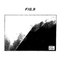
- Fig. 9 is a transition electron photomicrograph showing an enlargement of a grain boundary of adjacent crystal grains. Though no intergranular phase is observed in the boundaries of adjacent crystal grains, an aluminum oxide phase has been formed at the triple point.
- Fig. 10 is a graph showing a result of an analysis by EDS (Energy Dispersive X-ray Spectrometer) of a grain boundary of adjacent crystal grains with respect to the sintered body No. 11 of an embodiment of the present invention, and it shows that the yttrium exists in a trace amount. However, the peak of "C" is attributed to the contamination of the sample.
- Fig. 11 is a graph showing a result of an analysis by EDS of the inside of a crystal grain with respect to the same sample. No peak of yttrium is observed and it shows existence of a peak of oxygen.
- Figs. 12 and 13 are graphs respectively showing results of analyses by EDS of the inside of a crystal grain with respect to the sintered body No. 16 in a comparative example. No peaks of oxygen and yttrium are observed.
- Fig. 14 is a graph showing a result of an analysis by EDS of a grain boundary in the interface of crystal grains with respect to the same sintered body as the above. A conspicuous peak of yttrium is observed. This intergranular phase containing a large amount of yttrium contributes to increase the resistance between adjacent crystal grains.
- Fig. 15 is a graph showing a result of an analysis by EDS of a triple point with respect to the sintered body No. 16 in a comparative example. A further conspicuous peak of yttrium is observed.
- Fig. 16 is a graph showing an X-ray diffraction peak with respect to the sintered body No. 11 in an embodiment of the present invention. As is seen from this graph, there is no peak corresponding to crystals of an yttrium compound. Therefore, yttrium does not constitute a crystalline phase at the boundary of crystal grains.
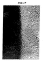
- Fig. 17 is a TEM photograph in a high magnification showing a crystal tissue near the grain boundary of adjacent crystal grains with respect to the sintered body No. 11 of an embodiment of the present invention.
- the crystal grains are present on the right and left hand sides, respectively, in this photograph, and an interface exists between crystal grains in the right and left directions.
- constituent atoms of a crystal lattice form a perfect orderly crystal lattice. It has been found that though the crystal lattice is slightly disordered in the vicinity of the grain boundary of the crystal grains, the width of the portion where the crystal lattice is disordered is extremely as narrow as about several numbers of atoms, that is, no more than 1 nm.
- Fig. 18 is a TEM photograph in a high magnification showing a crystal tissue near the grain boundary of adjacent crystal grains with respect to the sintered body No. 16 of a comparative example.
- a disorder of crystal lattice is recognized in the vicinity of the grain boundary between the right and left grains. Its width is about 1-3 nm. From the result of a restricted view field electron diffraction, crystalline precipitates were detected at the grain boundary. This disordering of the crystal lattice is assumed to be caused by fine precipitates deposited in grain boundaries.
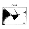
- Figs. 19 and 20 are transition electron photomicrographs with respect to the sintered body No. 16 in a comparative example. At the triple points and grain boundaries, black precipitates (0.2 ⁇ m) were observed. As a result of observation of the precipitates by EDS, Y 2 Al 4 O 9 was detected. Besides, these precipitates were crystalline.
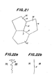
- the interface 6 between adjacent crystal grains 5A and 5B had an irregularly intermingled shape and was intricately bent.
- the width t of this intergranular phase was about 1-3 nm.
- the interface 2 between crystal grains 1A and 1B extended substantially straight, and the width was not more than 1 nm. Further, the deviation of the position of the grain boundary was on a level of several aluminum atoms.
- aluminum nitride sintered bodies of experimental run No. 51 - 63 shown in Tables 7 and 8 were produced.
- the starting powder aluminum nitride powder obtained by a reductive nitriding method was used. Amounts of oxygen and metal impurities in this starting powder are shown in Table 7 .
- Yttrium nitrate was dissolved in isopropyl alcohol to provide an additive solution. This additive solution was admixed with the aluminum nitride starting powder by using a pot mill. The amounts of the added yttrium as Y 2 O 3 are shown in Table 7.
- the total amount of metal impurities except yttrium was determined and shown in Table 7. Further, the content of yttrium (Y), a total oxygen content (O), a total carbon content (C), and excessive oxygen (the difference between the total oxygen content and the oxygen content in yttria) in the sintered bodies were shown in Table 7. Besides, the g-value, spin number, average particle diameter, thermal conductivity, strength, relative density and color were measured as aforementioned with respect to each sintered body. The results are shown in Table 8.
- the amount of yttria added to the starting powder was 5 % by weight, and in the sintered body it remained in an amount of about 3.7 % or 0.1 %, by weight.
- the oxygen content in the crystal particle was determined with an electron probe X-ray microanalyzer, and it was found to be 0.35 % or 0.21 %, by weight. Namely, since in experimental run No. 52 the hot press temperature was relatively higher, discharge of yttria proceeded on the sintering stage, and discharge of the oxygen from inside of the crystal particle also proceeded.
- the volume resistivity of the sintered body is in the order of 10 14 ⁇ cm in Comparative Example 51, and in the order of 10 12 ⁇ cm in Comparative Example 52.
- the volume resistivity is lower in Comparative Example 52. This is considered that grain growth proceeded with discharging yttria, more in Comparative Example 52.
- the amount of the oxygen in crystal grains determined by an electron probe X-ray microanalyzer is not less than 0.5 % by weight, and the amount of the "excessive oxygen” is also not less than 0.5 % by weight. Additionally, it has been found that most of the "excessive oxygen" is distributed within the crystal grains, except Examples 62 and 63.
- the present inventors measured a spectrum by cathode luminescence with respect to each of the sintered bodies, experimental run numbers of which are shown in the aforementioned Tables 1-8. As the result, it has been found that an extreme decrease of the volume resistivity is recognized as mentioned above, in the sintered bodies that exhibit an intense main peak at 350-370 nm.
- the surface of the sintered body of Example 54 was mirror-polished with diamond paste, then the spectrum was observed according to the cathode luminescence method. The result is shown in Fig. 23.
- the axis of ordinate shows an intensity of luminescence and the axis of abscissa shows a wavelength of luminescence. A strong peak has appeared in the wavelength range of 350-370 nm, and a weak peak has appeared in the wavelength range of 650-750 nm.
- the surface of the sintered body of Comparative Example 52 was mirror-polished with diamond paste, then the spectrum was observed according to the cathode luminescence method. The result is shown in Fig. 24. As the result, weak peaks at about 340 nm, 500 nm and 600 nm are observed, respectively.
- Fig. 25 is shown comparison of Example 54 with Comparative Example 52 with respect to spectra obtained according to the cathode luminescence method.
- the luminescence intensity of the main peak in 350-370 nm that is characteristically shown in the sintered body according to the present invention is very high, as compared with each peak of the sintered body of Comparative Example.
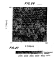
- Fig. 26 cathode luminescence two-dimensional mapping was conducted at a wavelength of 360 nm. The result is shown in Fig. 26. Besides, in Fig. 27 is shown a relationship between shades in the two-dimensional mapping shown in Fig. 26 and a luminescense intensity. Additionally, Fig. 28 is a scanning electron photomicrograph of a ceramic tissue with the same view field as Fig. 26.
- the shades in the two-dimensional mapping is considered to depend on the crystalline orientation of each crystal grain. Namely, in the case where a crystal grain has a crystalline orientation perpendicular to electron radiation, the luminescence intensity according to the cathode luminescence method is increased. Thus, the difference in crystalline orientation of each crystal grain shown in Fig. 28 may be a direct cause of variation of the shades shown in Fig. 26. Besides, in Fig. 26, a portion corresponding to the grain boundary is always dark and not luminous. From the above result of measurement, it has been found that a very strong luminescence at wavelength 360 nm is emitted from the inside of crystal grains.
- Metals can be embedded in the aluminum nitride sintered body according to the prevent invention.
- Articles embedded with an electrode can be used preferably particularly in an environment where impurities are abominated. Examples of such applications include: ceramic electrostatic chucks; ceramic heaters; and high frequency electrode apparatuses. The use for electrostatic chucks is particularly suitable.
- the metal embedded articles according to the invention are used as an electrostatic chuck, for example, for attracting semiconductor wafers, since a dielectric layer can be made to have a volume resistivity of not more than 1 x 10 12 ⁇ cm at room temperature, it may be possible to extremely improve attracting characteristics of the electrostatic chuck in the temperature range of around room temperature or below -60°C. In this case, even if the thickness of the dielectric layer is made to be not less than 500 ⁇ m, when voltage is applied, electric charge is transferred from the electrode onto the surface of the insulative dielectric layer, so that a sufficient attracting force can be obtained. Immediately after turning off the voltage, the electric charge is lost quickly. Therefore, the response for chucking or releasing wafer is also good. It has become possible thereby to attract and hold stably a large-sized semiconductor wafer of not less than 8 inches in the extremely wide temperature range from a low temperature region of particularly about -60°C to a high temperature region of not less than 300°C.
- Such a metal member to be embedded in the aluminum nitride sintered body is preferred to be a plate-type metal bulk material.
- the metal member when the metal embedded article is an electrostatic chuck, the metal member is a plate-type electrode made from the metal bulk material.
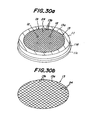
- the term "plate- type metal bulk material” should be understood to mean a monolitic plate-type material formed of metal, for example, as shown in Fig. 30, other than a spiral or zigzag shaped wire or plate.
- the metal member since it is fired together with aluminum nitride powder, is preferred to be formed of a high melting metal.
- a high melting metal include: tantalum; tungsten: molybdenum; platinum; rhenium; hafnium; and alloys thereof. From the viewpoint of preventing semiconductors from contamination, tantalum, tungsten, molybdenum, platinum and alloys thereof are more preferred.
- objects to be treated with electrostatic chucks include an aluminum wafer and the like, in addition to the semiconductor wafer.
- Examples of such a plate-type bulk material include the followings:
- the shape of the mesh and the wire diameter of such a metal net are not specifically limited. However, 150 meshes with wire of 0.03 mm diameter to 6 meshes with wire of 0.5 mm diameter could be employed without problems. Further, the cross sectional shape of the wire material constructing the metal net may be various rolled shapes such as circular, ellipse, rectangular and the like. Here, one mesh is meant by one wire per an inch.
- the electrodes of the electrostatic chuck can be connected with a high frequency power source to supply the electrodes with a high frequency voltage together with a DC voltage, whereby this electrode also can be used as an electrode for generating plasma.
- the thickness of the electrode is preferred to be not less than 430 ⁇ m.
- the electrode is formed of a metal bulk body.
- a dielectric layer having a thickness ranging 0.5 - 5.0 mm since a self-exotherm due to dielectric loss is not so high, can be used as a high frequency electrode with no problem.
- Fig. 29 is a cross sectional view schematically showing an embodiment of the electrostatic chuck.
- Fig. 30a is a perspective view showing the electrostatic chuck shown in Fig. 29, with a part cut away.
- Fig. 30b is a perspective view showing an electrode 13 formed of a metal net.
- a ring shaped flange 11c is provided on a circumferential side surface 11d of a substantially disc shaped substrate 11.
- An electrode 19 formed of a metal net 13 is embedded in the substrate 11.
- a dielectric layer 14 having a predetermined thickness is formed on the surface 11a for loading a semiconductor wafer 16.
- a terminal 20 is embedded in a supporting portion 18 of the substrate. One end surface of the terminal 20 is exposed at the rear surface 11b of the substrate 11.
- Through-holes 12 for inserting a pin for elevating and lowering the semiconductor wafer 16 are formed at predetermined positions of the substrate 11 .
- a DC power source 17 is connected via an electric wire 5A to the terminal 20, and a negative electrode of the DC power source 17 is connected via an electric wire 5B to the semiconductor wafer 16.
- the electrode 19 is formed of a metal net 13 as shown in Figs. 30a and 30b.
- the metal net 13 comprises a circular rim wire 13a and wires 13b arranged crosswise within the rim wire 13a, thus forming meshes 24 in the net.
- a resistance heating element 21 is embedded between the electrode 19 and the back surface 11b. Both the end portions of the resistance heating element 21 are connected to the terminals 22, respectively, and the terminals 22 are connected to the external terminals 23, respectively.
- This resistance heating element is for heating the semiconductor wafer during chucking the wafer and not always necessary.
- the aluminum nitride sintered body according to the invention can be used as a substrate for semiconductor manufacturing apparatuses, such as susceptors for holding a semiconductor wafer, dummy wafers, shadow rings. tubes for generating a high frequency plasma, domes for generating a high frequency plasma, high frequency transmitting windows, lift pins for supporting a semiconductor wafer, shower plates and the like.
- a heating source for induced heating (a heating material) can be exemplified.
- the sintered body according to the invention since it has a high purity as well as a high corrosive resistance against plasma, can be utilized as a heating source for induced heating to be used in a plasma atmosphere.
- the present inventors manufactured an electrostatic chuck as shown in Fig. 29.
- a starting powder an aluminum nitride powder obtained by a reductive nitriding method was employed.
- the amount of the oxygen was 1.2 % by weight and the amount of the metal impurities was 90 ppm in the starting powder.
- An additive solution was prepared by dissolving yttrium nitrate in isopropyl alcohol, and this additive solution was admixed with the aluminum nitride starting powder by using a pot mill.
- the proportion of the mixed yttria as Y 2 O 3 was 0.05 % by weight.
- a metal net 13 made of molybdenum was used as the electrode 19.
- the metal net 13 was knitted with a molybdenum wire having a diameter of 0.5 mm, at a density of 15 ends per 1 inch.
- the metal net 13 was embedded in the aforementioned starting powder, a pressure of 100 kgf/cm 2 was applied in a perpendicular direction of to the metal net 13 and axial press molding was conducted to provide a disc-type shaped body having a diameter of 200 mm.
- This disc-type shaped body was received in a hot press mold and sealed hermetically.
- the temperature was increased at a temperature increasing rate of 300°C/hour. In this case, the pressure was reduced in the range of from room temperature to 1000°C. Concurrently with the temperature increase up above this temperature range, the pressure was raised.
- the maximum temperature set at 2000°C was held for 5 hours.
- the total amount of the metal impurities except yttrium was 90 ppm
- the yttrium (Y) was 320 ppm
- the total oxygen (O) was 0.90 % by weight
- the total carbon (C) was 0.03 % by weight
- an excessive oxygen (O) was 0.89 % by weight.
- this sintered body had a g-value of ESR spectrum of 1.9977, a peak ratio (Al/Mn) of 3.50, a spin number of 2.9 x 10 13 spins/mg, an average grain diameter of 11 ⁇ m, a thermal conductivity of 60, a strength of 320 MPa, and a relative density of 99.9 %.
- the spectrum was measured by means of a cathode luminescence method, and the same main peak as that of Fig. 23 was observed in the wavelength range of 350-370 nm.
- the mount of the oxygen in crystal grains determined by an electron probe X-ray microanalyzer was 0.79 % by weight.
- the surface of the dielectric layer of the obtained sintered body was machined, to make the thickness of the dielectric layer 14 to be 1 mm.
- Through-holes 12 were perforated from the back surface side 11b of the sintered body with a machining center. Further, a terminal 20 was connected to electrodes 19. However, the resistance heating element was not embedded.
- the electrostatic chuck had a dimension of 200 mm diameter and 12 mm thickness. The attracting force of this electrostatic chuck was determined. The attracting force that was measured at an interval of 100°C from room temperature to 300°C was 60-100g/cm 2 at any temperatures. Besides, the volume resistivity at room temperature of the dielectric layer was 1 x 10 7 ⁇ cm.
- a novel aluminum nitride sintered body with a high purity and a low volume resistivity can be provided.
- a novel electronic functional material comprising such an aluminum nitride sintered body, which has a volume resistivity on a semiconductor level, and an electrostatic chuck using such an aluminum nitride sintered body.
Description
- The present invention relates to a novel aluminum nitride sintered body having a high purity and a low volume resistivity, and metal embedded articles, electronic functional materials and electrostatic chucks utilizing this aluminum nitride sintered body.
- At present, in film forming processes comprising the steps of transferring, exposing to light, chemical vapor depositing, sputtering and the like, and in the succeeding steps of micromachining, washing, etching, dicing and the like, of a semiconductor wafer, electrostatic chucks are used for attracting and holding the semiconductor wafer. As a substrate of such electrostatic chucks, dense ceramics have been drawing attention. Particularly, in apparatuses for manufacturing semiconductors, halogenous corrosive gases such as ClF3 and the like are frequently used as etching gases or cleaning gases. Moreover, in order that the semiconductor wafer is rapidly heated or cooled while being chucked, the substrate of the electrostatic chuck is desired to have a high thermal conductivity. It is further desired to have such a high thermal shock resistance that it may not fracture due to a rapid temperature change. A dense aluminum nitride has a high corrosive resistance against halogenous corrosive gases as mentioned above. Moreover, it has been known that such an aluminum nitride is a high thermal conductive material and its volume resistivity is not less than 1014Ω·cm at room temperature. Further, it is also known that aluminum nitride has a high thermal shock resistance. Therefore, it is accounted preferable to form a substrate of an electrostatic chuck for semiconductor manufacturing apparatuses of an aluminum nitride sintered body.
- On the other hand, in the semiconductor-manufacturing apparatuses, in order to use an electrostatic chuck as a susceptor for holding a semiconductor wafer, it is necessary to enhance the attracting force of the electrostatic chuck, and consequently it is necessary to decrease the specific resistance of the substrate. For example, in Japanese Patent Publication No. 7-19831, in order to increase the attracting force of the electrostatic chuck by decreasing the resistance of the insulating dielectric layer of the electrostatic chuck, an insulating material having a high volume resistivity is incorporated with a conductive or semiconductive material to adjust the resistivity of the insulating dielectric layer to not more than 1013Ω·cm. Moreover, in Japanese Patent Laid-Open Publication No. 2-22166, ceramics starting materials containing alumina as a main component are fired in a reducing atmosphere to produce dielectric ceramics for electrostatic chucks. In this case, the ceramic starting material is made to contain an alkali earth metal and a transition metal in amounts as oxide of 1-6 % and 0.5-6 %, by weight, respectively. In this method, for example, it is intended to increase the dielectric constant, concurrently decreasing the volume resistivity to 1012 - 1018Ω·cm, by incorporating TiO2 with the alumina ceramics, thereby to obtain a high attracting power.
- However, according to such a method, there will be posed problems such that products produced by corrosion of alkali earth metals and transition metals yield particles.
- However, highly purified aluminum nitride sintered bodies are not suited for forming a substrate of electrostatic chucks for semiconductor-manufacturing apparatuses, because of such a high volume resistivity thereof as at least 1014Ω·cm. In order to provide them with a sufficient attracting force, it is necessary to form an extremely thin insulating dielectric layer, 300 µm thick or less. However, it has been found that when such a thin insulating dielectric layer contacts with halogenous corrosive gas or plasma, during its long time use, there is a possibility of causing an insulation breakdown and the like occurring from a starting point on any of reactant layers on the surface of the insulating dielectric layer. From this point of view, it has been found that the insulating dielectric layer is preferred to be 500 µm thick or more.
- US-A-5376601 discloses a sintered aluminium nitride article. The article has high purity and an average grain size of greater than 9 µm. A sintering aid is not used.
- FR-A-2637887 discloses a fine powder of aluminium nitride. The mean particle diameter is not greater than 2 µm and at least 70% of the particles have a diameter of not greater than 3 µm. The powder comprises 93% by weight aluminium nitride, 0.02 to 5% by weight of oxides (e.g. alkaline-earth metals or lanthanum or yttrium family metals) and other components.
- However, in conventional electrostatic chucks made of an aluminum nitride sintered body, such a thick insulating dielectric layer results in decrease of the attracting force of the electrostatic chucks. Particularly in a low temperature region where a volume resistivity is high, it has been difficult to provide a sufficient attracting force. Particularly, it is at a low temperature of from -50°C to -60°C that dry etching processes are conducted, and it is at relatively a low temperature of around 100°C that highly densified plasma CVD processes are conducted. Therefore, in such low temperature processes, it has been difficult to constantly provide a predetermined attracting force.
- For this reason, the present inventors have restudied the aluminum nitride sintered bodies per se.
- For example, in an electrostatic chuck comprising an aluminum nitride substrate, the effect of adding a low resistivity material to the aluminum nitride substrate was studied according to the description in Japanese Patent Publication No. 7-19831. By this method, the volume resistivity of the aluminum nitride sintered body was able to be reduced to not more than 1013Ω·cm. However, with this electrostatic chuck, there is a possibility of causing pollution to semiconductor by separation of the added low resistant metal or the like from the surface of the substrate.
- Alternatively, it has been proposed to improve a thermal conductivity as well as a density of aluminum nitride by adding an oxide or carbonate of a rare earth element such as yttrium or the like, as a sintering assistant, to an aluminum nitride starting material (Japanese Patent Publication No. 63-46032). Using such a sintering assistant, dense aluminum nitride sintered bodies can be manufactured even by a normal pressure sintering method. However, such aluminum nitride sintered bodies have a high volume resistivity, and even those of about 99 % relative density have a volume resistivity on a level of 1013-1015Ω·cm.
- It is, therefore, an object of the present invention to provide a novel aluminum nitride sintered body having a high purity and a low volume resistivity.
- It is another object of the present invention to provide a novel electronic functional material comprising such an aluminum nitride sintered body and having a volume resistivity on the same level as that of semiconductors, and an article using such an aluminum nitride sintered body, with a metal member embedded therein.
- According to the first aspect of the invention, there is provided an aluminum nitride sintered body as set out in
claim 1. - Further, according to another aspect of the invention, there is provided an article as set out in claim 5.
- Furthermore, according to another aspect of the invention, there is provided an electronic functional material as set out in
claim 6. - The present inventors, in the course of manufacture of an aluminum sintered body containing not more than 900 ppm of at least one metal impurity other than rare earth elements, have surprisingly succeeded in providing an aluminum nitride sintered body with a volume resistivity of not more than 1 x 10¹²Ω·cm by adjusting the content of the rare earth elements (as oxides thereof) in the sintered body to not more than 0.5 % by weight, and making the sintering to proceed so that constituent aluminum nitride crystal grains may have an average grain diameter of at least 3.0 µm. The reason for such a result is not clear, but it can be conjectured as follows:
- As a basic way of thinking, the resistance of aluminum nitride sintered bodies can be calculated as a resistance of a circuit formed by connecting aluminum nitride crystal grain resistances with grain boundary resistances in series and parallel. The present inventors have accelerated densification of a sintered body, by employing aluminum nitride particles with high purity, admixing a small amount of a rare earth element therewith, and applying a high pressure by means of hot pressing or the like.
- In this case, if the rare earth element compound is admixed in an amount of more than 0.5 % by weight, oxygen existing in the starting particles diffuses towards the outside of the particles during firing. In contrast therewith, according to the present invention, by adjusting the amount of the rare earth element compound to small, and applying a high pressure during sintering, the oxygen is made to remain in aluminum nitride crystal grains in the state of solid solution. This oxygen in the crystal grains replaces nitrogen atoms in AlN, to form a donor level in a band gap, with the consequence that the electron conductivity in the grains is improved. As mentioned above, the oxygen solid-solution in aluminum nitride crystal grains is essential for decreasing the resistance of each crystal grain.
- Conventionally, rare earth elements such as yttrium or the like have been incorporated, as a sintering assistant, with aluminum nitride sintered bodies in an amount as oxide thereof of several percent by weight (Japanese Patent Publication No. 63-46032). If this amount is positively decreased, a dense body becomes hardly obtainable in normal pressure sintering. Besides, a study has been conducted to improve a thermal conductivity of aluminum nitride sintered bodies by increasing the amount of these sintering assistants to be added. That is to say, it has been a common sense to add about several % by weight of a sintering assistant in order to decrease porosity and increase thermal conductivity of aluminum nitride sintered bodies.
- Further, the starting powder of aluminum nitrides contains oxygen within the particles thereof. The oxygen existing in the inside of each particle diffuses towards the outside of the particles by virtue of an action of the sintering assistant during sintering. It has been assumed that the thermal conductivity is more improved with progressing process of discharging the oxygen from the aluminum nitride particles.
- Namely, it has been considered that the oxygen atoms are a kind of impurities which remain in the aluminum nitride crystal grains even after sintering. Accordingly, a study to decrease the amount of oxygen remaining in the grains has been conducted in order to improve the thermal conductivity of sintered bodies. From another point of view, a study for utilizing aluminum nitride sintered bodies as a material having a volume resistivity in the region of semiconductors has not been heretofore conducted.
- In contrast, according to the present invention, the amount of the oxygen remaining in grains after pressure sintering, is controlled by adjusting the amount of the rare earth element compound blended and increasing the pressure during sintering, with the consequence that the oxygen is made to remain as a donor for decreasing the resistance of each crystal grain. It is an utterly novel concept that the oxygen remaining in crystal grains after sintering is used as a donor, in order to decrease the volume resistivity of aluminum nitride sintered bodies to the same level as semiconductors.
- The content of the rare earth element(s) in aluminum nitride sintered bodies is necessary to be not more than 0.5 % by weight as oxide thereof. If it exceeds 0.5 % by weight, the oxygen existing in crystal grains diffuses toward the outside of the grains during sintering. If the oxygen is thus purged out and the interior of the grains is purified, the thermal conductivity is increased by virtue of decrease of phonon scattering with decreasing oxygen, but the resistance of each grain is also increased. Further, rare earth elements remaining at boundaries and triple points of each aluminum nitride crystal grain form an intergranular phase. This intergranular phase disorders the crystal lattice near the grain boundary of each aluminum nitride crystal grain adjacent to others, and loosens adhesion between crystal grains. It is considered that the decrease of the volume resistivity of the sintered body has so far been impeded by such disordering at each grain boundary of crystal grains. In the aluminum nitride sintered bodies according to the present invention, even the disorder of atom arrangement at the aluminum nitride crystal grain boundary can be hardly seen.
- From this point of view, the volume resistivity of the sintered bodies can be more lowered by decreasing the content of the rare earth elements to not more than 0.1 % by weight.
- It is necessary that the content of the rare earth elements in the sintered body is made to be not less than 150 ppm. It has been found that if it is made to be not less than 300 ppm, the decrease of the volume resistivity becomes particularly noticeable. From this point of view, the content of the rare earth elements in the sintered body is more preferred to be not less than 300 ppm.
- Particularly for use in semiconductor processes, alkaline metals and transition metals which are regarded as impurities in these processes are not preferred. Further, it is considered that metal impurities except rare earth elements are present inside the grains or at grain boundaries and function to increase an in-grain resistance or grain boundary resistance.
- Further, in the present invention, it is necessary to employ starting materials with high purity, more concretely, the content of metal impurities except rare earth elements must be restricted to not more than 900 ppm. If it exceeds 900 ppm, the tendency to increase the volume resistivity of the sintered body is shown as conceived. Since these metals are included as impurities, it is preferred to be as small an amount as possible. Accordingly, the amount of the metal impurities except rare earth elements is preferred to be not more than 500 ppm, more preferably not more than 100 ppm, including 0 ppm to below a detectable limit.
- Further, the average grain diameter of the aluminum nitride crystal grains in the sintered bodies is to be not less than 3.0 µm, more preferably not less than 4.0 µm, and most preferably not less than 5.0 µm.
- If the average grain diameter of the crystal grains increases, the number of the crystal grain boundaries per unit length of the conduction path in the sintered body decreases. In general, the resistance of the crystal grain boundary is larger than that in the crystal grains, for example, in the case where the sintering temperature is increased to grow crystals, a tendency to decrease volume resistivity thereof is shown. It is important to decrease the number of the grain boundaries per the number of the grains, in order to decrease the volume resistivity of the sintered body. Therefore, if the crystal grains have grown to have an average grain diameter only up to less than 3.0 µm, since the frequency of the grain boundaries per conduction path increases, the resistivity of the sintered body also increases.
- There is no particular upper limit in the average diameter of the aluminum nitride crystal grains, it is generally preferred to be not more than 20 µm,
- Further, the aluminum sintered bodies have a relative density of not less than 98.5 %, whereby the volume resistivity of the sintered bodies is further decreased. From this point of view, the relative density of the sintered body is preferred to be not less than 99.0 %, more preferably not less than 99.6 %.
- As mentioned above, in the present invention, the aluminum nitride sintered bodies are required to be extremely densified, and at the same time, the amount of the rare earth elements added is decreased to such an amount that the rare earth elements substantially may not act as a sintering assistant. At the same time, the amount of other metal elements to be added which is functionable to promote sintering is required to be decreased to the utmost as mentioned above. Under such a condition, generally only a relative density of not more than 90 % can be obtained by means of normal pressure sintering.
- Therefore, in order to obtain the aluminum sintered bodies according to the present invention, it is necessary to employ a press sintering process such as a hot press process and a hot isostatic press process, whereby the aluminum nitride sintered bodies can be densified without requiring any sintering assistant.
- Thus, one of the principal points of the present invention is that a mechanical pressure is also applied during firing. For example, according to the conventional concept, the hot press process has been understood as a process for applying a mechanical pressure for promoting densification of sintered bodies.
- However, in the present invention, it is not only for promoting densification of sintered bodies. Namely, under a high temperature condition during firing, there is a possibility such that the electron state of the aluminum nitride crystal grains or grain boundaries is interfered synergistically with small amounts of rare earth elements having existed at the surface of the aluminum nitride grains from prior to firing, which would not occur in a normal pressure sintering. It is assumed that such an interference controls the arrangement of aluminum atoms and nitrogen atoms at the boundaries of adjacent crystal grains and thus decreases the resistance at the grain boundaries. It is highly possible that the above causes the decrease of the resistance at the grain boundaries, and also may effect in decrease of the in-grain resistance.
- The thus obtained aluminum nitride sintered bodies according to the present invention surprisingly have a volume resistivity in the range of 1 x 10¹²-1 x 10⁶Ω·cm, particularly not more than 1 x 10¹¹Ω·cm, and more particularly not more than 1 x 10¹⁰Ω·cm. Such a range of the volume resistivity belongs just in the region for semiconductors. The present invention, in highly pure aluminum nitride sintered bodies including very small amounts of metal impurities and rare earth elements, first provides a sintered body having a volume resistivity of semiconductor region. In this respect, the present invention is epoch-making.
- Further, the aluminum nitride sintered bodies have hitherto been studied as an electrically insulating material with a high thermal conductivity. Furthermore, an attempt has been made to decrease the resistance by doping aluminum nitride sintered bodies with an electric conductor or semiconductor. However, a study has not been conducted to decrease the resistance of the aluminum nitride crystal grains per se, like the present invention.
- The present inventors have further investigated boundaries of each crystal grains, and have searched into the reason for the drastic decrease of the volume resistivity of the sintered body. First, in the case where no rare earth element was added as described above, the volume resistivity of the sintered body was not so decreased as the case of the present invention, and rare earth elements did not form solid- solution in the crystal grains, so that it is conjectured that if a very small amount of rare earth elements existed in the boundaries of adjacent crystal grains, the resistance at the crystal grain boundaries could be decreased.
- In fact, the present inventors have found by each measuring method as mentioned below that rare earth elements substantially do not exist within the aluminum nitride crystal grains, but are present in the boundary of two aluminum nitride crystal grains adjacent to one another. In this specification and claims, that the phrase "rare earth elements substantially do not exist in crystal grains" should be understood to mean that there is shown no peak corresponding to rare earth elements by means of EDS (Energy Dispersive X-ray Spectrometer).
- It has been found that the rare earth elements exist in the grain boundary of adjacent two aluminum nitride crystal grains but do not form a crystalline phase, and are present in the grain boundary between crystal grains on an atomic level. And it has been found that in the grain boundary of adjacent two aluminum nitride crystal grains, the disordered portion of the crystal lattices composing each aluminum nitride crystal grain can hardly been observed, and that the width of this portion is not more than 5 nm, particularly not more than 1 nm. In some measured samples, such a disorder of the crystal lattices at interfaces of the grains substantially could not be observed. It is conjectured that the resistance between crystal grains is extremely decreased, because of such a specific microstructure at the grain boundary of the crystal grains.
- Further, the present inventors have investigated the triple point (triple point formed by three aluminum nitride crystal grains) in the aluminum nitride sintered bodies, and found that the crystalline phase at the triple point substantially does not contain rare earth elements. From this result, it is conjectured that the rare earth elements exist, as an extremely thin amorphous phase, near the surface or on the surface of each aluminum nitride crystal grain. Even at the triple point, it has been found that rare earth elements exist only near the surface or on the surface of the crystal grains.
- From these results, it has been elucidated why the volume resistivity is extremely increased in the case where much metal impurities except rare earth elements are included. It is because that such a metal atom impurity forms solid-solution within the aluminum nitride crystal grains or exists in the grain boundaries, and such crystal grains or grain boundaries are considered to have a high resistance.
- Further, the difference between a total oxygen content in an aluminum nitride sintered body and an oxygen content in the assumed oxides of rare earth elements is not less than 0.5 % by weight. This difference represents the content of the oxygen remaining in the aluminum nitride crystal grains. By increasing this up to not less than 0.5 % by weight, the resistance of the crystal grains per se can be decreased, whereby the volume resistivity of the whole sintered body also can be extremely decreased. However, the upper limit is 2.0 % by weight.
- The present inventors have taken spectra by means of an electron spin resonance method (ESR method) with respect of each sample of the aluminum nitride sintered bodes having a low volume resistivity according to the invention, in order to study the constitution of the defect structure of inside the crystalline phase and at the grain boundary. This principle will be explained briefly. Under a magnetic field, an energy level of unpaired electrons is split due to the Zeeman's effect. To these energy levels sensitively react an orbit movement of electrons and a mutual action of neighboring electrons with a nuclear magnetic efficiency. In the ESR method, it is possible to obtain information about atoms, chemical coupling or the like in the vicinity of an atom having the unpaired electrons, by measuring the split energy levels.
- In the aluminum nitride, the g-value of the unpaired electrons of aluminum varies corresponding to a crystal field where the unpaired electrons exist. This g-value is 2.0000 theoretically in a free electron, and 2.002316 after a relativistic correction. The Al atom and N atom in the aluminum nitride crystalline phase have a wurtzite structure with four coordinations. Therefore, an sp3 hybridized orbit is constructed by one aluminum atom and three nitrogen atoms. It is possible to know, from the g-value of each sample, what crystal coordination that unpaired electrons in the lattice defects exist in or what kind of elements exist around the unpaired electrons.
- From this result, it has been proved that in the aluminum nitride sintered bodies according to the present invention, the g-value of the unpaired electrons of the aluminum in a spectrum by means of ESR method is not more than 2.000.
- If the kind of atoms coupled with an Al atom having unpaired electrons is varied, the g-value will be largely varied. The cause for resulting such a low g-value as the above is attributable to a variation of the kind of atoms coupled with the aluminum. In a Si atom having a four coordinate structure, it has been reported that the same variation of the g-value as the above occurs (see: "ESR assessment method of materials", IPC Publishing, page 57). This reason is conjectured to be due to an influence of oxygen atoms remaining in aluminum nitride crystal grains.
- It has also been found that the spin amount per unit mg of aluminum obtained from a spectrum by means of ESR method is not less than 1 x 10¹³ spin. The measuring method was according to the method described in Hiroaki Ohya and Jun Yamauchi: "Electron Spin Resonance" published by Kodansha Co., Ltd. That is, the absorption intensity in ESR spectra is proportional to the percentage of unpaired electrons in the aluminum nitride crystal grain. The quantitative determination of the g-value needs to be conducted comparing with a standard sample having a known g-value. Namely, it is necessary that the sample having a known g-value and the sample of the aluminum nitride sintered body according to the present invention are measured under the same condition, absorption curves obtained are converted into integral curves, and then areas defined by the integral curves are compared with each other.
- The present inventors quantitatively determined a single super fine line of Mn2+/MgO by using a solution of TEMPOL (4-hydroxy-2,2,6,6-tetramethylpyperidine-1-oxyl) having a known spin amount, compared the spin amount with the line, and calculated the spin amount per unit mg of the aluminum nitride sintered body from an area ratio of peaks.
- In order to estimate the state of the electrons in the band gap affecting on the electric property of the aluminum nitride sintered body and further clarify the feature of the present invention, the inventors measured a cathode luminescence spectrum.
- A cathode luminescence is generally a kind of reflection waves from a sample when it is irradiated with an electron ray. As shown in Fig. 1 as a schematic view, if an excited electron exits from a valence band to a conduction band, a positive hole is formed in the valence band. Then, luminescence corresponding to a band gap between the valence band and the positive hole in the valence band is emitted. In addition, in the case where a local electron level other than the conduction band is generated by a function of defects or impurities included in the crystal, luminescence is emitted by virtue of re-coupling of excited electrons in the local electron level with the positive holes in the valence band. Therefore, it is possible to obtain information about an energy band structure, a crystal property and defects and impurities included in the crystal from the cathode luminescence spectrum.
- A cathode luminescence spectrum of the sintered body according to the present invention was measured. As the result, as shown in Figs. 23 and 25, it was found that a strong main peak existed in the wavelength range of 350 -370 nm. Further, a weak peak, which was assumed as a double multiple wave of the main peak, was detected in a wavelength range of 650-750 nm.
- Further, as a comparative object, a highly densified sintered body was prepared by admixing an aluminum nitride powder with 5 % by weight of yttria powder and firing. With respect to this sintered body, a cathode luminescence spectrum was measured. As the result, for example, as shown in Figs. 24 and 25, weak peaks were observed at wavelengths of about 340 nm, 500 nm and 600 nm, respectively.
- Such a difference in the wavelength of luminescence represents a difference of kinds of luminescence i.e. an electron level in the band gap. Alternatively, a difference in intensity of luminescence shows a difference of electron density due to impurities. That is, in the sintered body according to the present invention, a very strong and sharp peak was observed in the wavelength range of 350 - 370 nm. This shows existence of a very strong new electron level and a high electron density due to a particular impurity.
- Then, the inventors conducted a cathode luminescence two-dimensional mapping with respect to luminescence of 360 nm wavelength, in order to specify whether an electron level generating a strong main peak in the wavelength range of 350 -370 nm exists in aluminum nitride crystal grains in the sintered body or in the intergranular phase of the crystal grains.
- Then, the result of this mapping was compared with a scanning electron photomicrograph with respect to the same view field of the same sample. It was proved that a very strong luminescence of 360 nm wavelength by cathode luminescence existed in the aluminum nitride crystal grains. On the other hand, grain boundary portions were dark, and the above mentioned luminescence could not be seen. This shows that regions of high electron density i.e. regions of high local electron level, are distributed within the grains and not in the intergranular portions. From this result, it has been found that the electric property of the crystal grains per se has a strong influence upon the volume resistivity of the sintered body.
- Further, distribution of oxygen density was measured by means of an electron probe X-ray microanalyzer (EPMA) with respect to the sintered bodies of the present invention. As the result, it has been found that in the sintered bodies of the present invention, a relatively large amount of oxygen forms solid-solution in the grains.
- In the sintered bodies of the present invention, it is assumed that a relative large amount of oxygen forms solid-solution in the aluminum nitride crystal grains, and this provides the local electron level and contributes to decreasing the in-grain resistances. This is in accordance with the high intensity of the absorption peak on the ESR spectrum.
- Concretely, as a result of determination of the oxygen concentration in the aluminum nitride crystal grains constituting the sintered bodies according to the invention, it has been found that a concentration of not less than 0.5 %, preferably not less than 0.6 %, by weight, is required. It has no particular upper limit, but it is preferred to be not more than 2.0 %, more preferably no more than 1.0 %, by weight.
- In summarizing the experimental results mentioned above, it is conjectured that the electric resistance of crystal grains may be decreased according to the following process. Namely, when oxygen forms solid-solution in aluminum nitride crystal grains, the oxygen replaces nitrogen at a nitrogen lattice site. In this case, because of a compensation of an electric charge between nitrogen N3- and oxygen O2-, a conductive electron (donor) or a vacancy is formed in the aluminum lattice, which influences largely upon the electric conductivity. It is considered that the formation of such conductive electron or vacancy in the lattice decreases internal electric resistance of the aluminum nitride crystal grains and largely contributes to decrease the electric resistance of the sintered body.
- The present inventors also determined the distribution of the oxygen concentration by means of electron probe X-ray microanalyzer (EPMA) with respect to a comparative object sintered body admixed with 5 % by weight of yttria. As the result, in the case of the sintered body admixed with 5 % by weight of yttria, the internal oxygen concentration of the crystal grains was decreased relatively. Moreover, it has been found that a portion including relatively much oxygen almost overlaps a portion containing yttria. It has been known that yttria does not form solid-solution in aluminum nitride grains and is discharged to intergranular portions. Accordingly, most oxygen atoms are not present in the grains but a grain boundaries.
- Therefore, in the course of sintering progress, the yttrium is discharged from the grains, when the yttrium shows a tendency to entrain oxygen atoms towards grain boundaries. Therefore, it is considered that oxygen atoms in the grains have been decreased.
- Next, a method for producing the sintered bodies according to the present invention will be explained. As an aluminum nitride starting powder, the powder obtained by a direct nitriding method as well as a reductive nitriding method can be used. At present, the powder by the reductive nitriding method is more preferred, since this method readily yields a powder having a low metal impurity content. However, even the powder obtained by a direct nitriding method can be used with no problem, if the purity of aluminum raw materials is improved and inclusion of impurities is prevented in each step of the manufacturing process.
- In the finally resulting sintered bodies, since the difference between the total oxygen content in the aluminum nitride sintered body and the oxygen content in oxides of rare earth elements is preferred to be not less than 0.5 % by weight, the oxygen content in the starting powder is rather important. When the oxygen content in the starting powder is low, a post-treatment for introducing oxygen into the starting powder becomes required. For example, the oxygen content in the starting powder can be increased by an oxidation treatment in which the starting powder is heated at a temperature of 400 - 800°C in oxidative atmosphere such as air. Alternatively, the starting powder can be admixed with various kinds of alumina powder or an alumina precursor.
- Finally, the difference between the total oxygen content in the aluminum nitride starting powder and the oxygen content in oxides of rare earth elements before subjecting to caramelizing and firing steps is preferred to be not less than 0.5 % by weight.
- However, in order to uniformly disperse oxygen atoms in each aluminum nitride crystal grain which constitutes a sintering body, it is preferred to make the oxygen content in the starting powder sufficiently high as mentioned above on the stage where the starting powder has been produced, without conducting the post-treatment as mentioned above.
- Further, the above starting powder can be admixed with rare earth elements in various forms. For example, the aluminum nitride starting powder can be admixed with powder of a simple substance or a compound of rare earth elements.
- Generally, oxides of rare earth elements are most readily available. However, in the case where oxides of rare earth elements are employed, the amount of the adding rare earth elements is very small in the present invention and, therefore, if dispersibility of the oxides of rare earth elements is insufficient, it will be difficult to uniformly disperse the rare earth elements over the whole sintered body, whereby various properties such as volume resistivity or the like in each portion of the sintered body are caused to vary.
- Therefore, in the present invention, compounds such as nitrates, sulfates, alkoxides or the like of rare earth elements are dissolved in an appropriate solvent in which these compounds are soluble, to thereby obtain solution and this solution can be admixed with the aluminum nitride starting powder. Thereby, even if the rare earth elements are added in a trace amount, the rare earth elements are uniformly dispersed to every portion in the sintered body. Moreover, since it is most probable that rare earth elements are dispersed on the surface of each grain as a very thin layer, the high resistant rare earth element compounds become difficult to precipitate partially. If dispersion is insufficient, it may occasionally happen that the crystals comprising rare earth elements are precipitated locally. A small ratio of precipitates will not influence upon the above requirements.
- When a dry press shaping process is employed, a spray dry process can be proposed as a process for drying the aforementioned starting powder. This process is particularly preferred as an instant drying process for compounds of rare earth elements as a trace additive.
- Alternatively, a tape shaping process may be employed. In this case, solution obtained by dissolving compounds such as nitrates, sulfates and alkoxides or the like of rare earth elements may be added as an additive into a conventional tape shaping step. Because of very small loads, there will be no influence upon the shapability and dewaxability.
- In a blending stage, an aluminum nitride starting powder is dispersed in a solvent, with which can be admixed rare earth element compounds in the form of oxide powder or solution as mentioned above. The mixing may be conducted by simple stirring. However, in the case where pulverization of aggregates in the starting powder is required, mixing pulverizing machines such as pot mill, trommel, attrition mill or the like may be employed. In the case where an additive soluble in a solvent for pulverization is employed, the time for conducting the mixing and pulverizing steps may be the shortest time required for the pulverization of the powder. Besides, binders such as polyvinyl alcohol or the like may be added.
- A spray dry process is preferred for the step of drying the solvent for pulverization. Alternatively, after conducting a vacuum drying process, it is preferred to adjust the grain size by passing the dry powder through a sieve.
- In the powder shaping step, when a disc-type shaped body is manufactured, a mold pressing process may be employed. A shaping pressure is preferred to be not less than 100 kgf/cm2, and, however, it is not particularly limited, as far as the mold can be maintained. The hot press mold also can be loaded with a shaping material in a powdery form.
- When a binder is admixed with a shaped body, the dewaxing may be conducted at a temperature of 200 - 800°C in an oxidative atmosphere prior to firing.
- In the case where an additive containing rare earth elements in the form of nitrates, sulfates and carbonates is added, denitrification, desulfurization and decarboxylation may be conducted for the starting powder or powdery shaped body, prior to firing. Such a degassing step may be conducted by heating the abovementioned starting powder or powdery shaped body under oxidative atmosphere, like the dewaxing step. In this case, it is necessary, however, to pay attention to damage of furnaces by NOx gases, SOx gases and the like.
- Alternatively, the degassing may be conducted during firing, without conducting separately the degassing step such as denitrification, desulfurization, decarboxylation or the like.
- Then, the shaped body is fired by means of a hot press process. The pressure in the hot pressing is required to be not less than 50 kgf/cm2, preferably not less than 200 kgf/cm2. There is no particular upper limit. However, in order to prevent the damage of the furnace, it is preferred to be not more than 1,000 kgf/cm2, more preferably not more than 400 kgf/cm2 from a practical point of view.
- When the pressure is increased, it is possible to increase up to a maximum pressure all at once. However, it is particularly preferred to increase the pressure stepwise as the temperature rises, in order to improve the precision of the sintered body.
- When a disc-type shaped body is fired by means of a hot press process, it is preferred to receive the shaped body in a sleeve having an inside diameter slightly larger than the outside diameter of the shaped body.
- When degassing is required in the temperature increasing step, it is preferred to promote exhalation of gases by heating under vacuum in the temperature range from room temperature to 1,600°C.
- Additionally, it is preferred to increase the temperature at a temperature increasing rate from between 50°C/ hour and 1,500°C/hour up to a maximum temperature in firing. The maximum temperature is preferred to be 1,750 - 2,300°C. If the maximum temperature exceeds 2,300°C, aluminum nitride begins to decompose. If the maximum temperature is less than 1,750°C, the effective grain growth is restrained, and the average grain diameter will not reach 3 µm.
- Further, as regards the time for sintering the shaped bodies, with the maximum temperature in the range from 1,850°C to less than 1,900°C, the sintering was required to be conducted for at least 3 hours. Even at a maximum temperature from 1,900°C to less than 2,000°C, the maximum temperature was necessary to be retained for not less than 2 hours. Further, when the retention time was made to be not less than 3 hours, or not less than 5 hours, a further decrease of volume resistivity was observed. When a maximum temperature of not less than 2,000°C was retained for not less than 1 hour, a decrease of volume resistivity was observed. The retention time is preferred to be not more than 30 hours from the viewpoint of practical productivity in sintering furnaces. Cooling was conducted at a cooling rate of 300°C/hour from a maximum temperature to 1,400°C. Then, at 1,400°C, the power source was turned off, to allow spontaneous cooling. The influence of the cooling rate on resistance is not clear.
- In the hot press process, there has now been proposed a process wherein boron nitride as a parting agent is applied between a shaped body or starting powder and a carbon jig. However, in the present invention, since there is a fear of inclusion of boron into the sintered bodies, use of the parting agent is not preferred.
- The above and other objects, features and advantages of the present invention will become more apparent from reading the following description of the preferred embodiments taken in connection with the accompanying drawings, wherein:
- Fig. 1 is a schematic view illustrating a principle of cathode luminescence;
- Fig. 2 is a graph showing a relationship between an amount of metal impurities except yttrium and volume resistivity;
- Fig. 3 is a graph showing a relationship between an amount of added Y2O3 and a volume resistivity of a sintered body;
- Fig. 4 is a graph showing a relationship between an amount of excessive oxygen and a volume resistivity;
- Fig. 5 is a graph showing a relationship between a g-value obtained from an ESR spectrum and a volume resistivity;
- Fig. 6 is a graph showing a spin amount based on an ESR spectrum and a volume resistivity;
- Fig. 7 is a scanning electron photomicrograph showing a ceramic tissue with respect to the sintered body of the Example 11;
- Fig. 8 is a transition electron photomicrograph showing an enlargement of a ceramic tissue around a triple point of the sintered body shown in Fig. 7;
- Fig. 9 is a transition electron photomicrograph showing an enlargement of a grain boundary of adjacent crystal grains with respect to the sintered body of an embodiment of the present invention;
- Fig. 10 is a graph showing a result of an analysis by EDS of a grain boundary of adjacent crystal grains with respect to the sintered body of an embodiment of the present invention;
- Fig. 11 is a graph showing a result of an analysis by EDS of the inside of a crystal grain with respect to the sintered body shown in Fig. 10;
- Fig. 12 is a graph showing a result of an analysis by EDS of the inside of a crystal grain with respect to a sintered body of a comparative example;
- Fig. 13 is a graph showing a result of an analysis of EDS of the inside of a crystal grain with respect to a sintered body of a comparative example;
- Fig. 14 is a graph showing a result of an analysis by EDS of a grain boundary of adjacent crystal grains with respect to the sintered body shown in Fig. 12;
- Fig. 15 is a graph showing a result of an analysis by EDS of a triple point with respect to a sintered body of a comparative example;
- Fig. 16 is a graph showing an X-ray diffraction peak with respect to the sintered body of an embodiment of the present invention;
- Fig. 17 is a TEM photograph of a ceramic tissue in a high magnification showing a crystal tissue in the vicinity of a grain boundary of adjacent crystal grains with respect to the sintered body of an embodiment of the present invention;
- Fig. 18 is a TEM photograph of a ceramic tissue in a high magnification showing a crystal tissue in the vicinity of a grain boundary of adjacent crystal grains with respect to a sintered body of a comparative example;
- Fig. 19 is a transition electron photomicrograph showing a ceramic tissue of a sintered body of a comparative example;
- Fig. 20 is a transition electron photomicrograph showing a ceramic tissue of a sintered body of another comparative example;
- Fig. 21 is a schematic view showing a feature of microstructure of the sintered body of an embodiment of the present invention;
- Fig. 22a is a schematic view illustrating the state of the grain boundary of adjacent crystal grains with respect to a sintered body of a comparative example;
- Fig. 22b is a schematic view illustrating the state of the grain boundary of adjacent crystal grains with respect to the sintered body of an embodiment of the present invention;
- Fig. 23 is a spectrum obtained by cathode luminescence with respect to the sintered body of an embodiment (Example 54) of the present invention;
- Fig. 24 is a spectrum obtained by cathode luminescence with respect to the sintered body of Comparative Example 52;
- Fig. 25 shows spectra obtained by cathode luminescence, respectively of the sintered bodies of Example 54 and Comparative Example 52;
- Fig. 26 is a photograph showing a cathode luminescence two-dimensional mapping of the sintered body of Example 54;
- Fig. 27 is a photograph showing a relationship between shades in a cathode luminescence two-dimensional mapping and luminescence intensity;
- Fig. 28 is a scanning electron photomicrograph of a ceramic tissue in the same view field as Figure 26 with respect to the sintered bodies of Example 54;
- Fig. 29 is a cross sectional view schematically showing an example of electrostatic chuck; and
- Fig. 30a is a slant view showing a principal portion partially cut away of the electrostatic chuck shown in Fig. 29; and
- Fig. 30b is a slant view showing an example metal net usable as an electrode for an electrostatic chuck.
- The present invention will be explained in more detail hereinafter by way of example and with reference to experimental results. The examples are not intended to limit the invention.
- Each aluminum nitride sintered body shown in Tables 1-6 was produced. As the starting powder, aluminum nitride powder obtained by a reductive nitriding method was used. And amounts of oxygen and metal impurities in the starting powder are shown in Tables 1, 3 and 5. An additive solution was prepared by dissolving yttrium nitrate in isopropyl alcohol, and the additive solution was admixed with the aluminum nitride starting powder, using a pot mill. Mixing ratios of the yttrium as Y2O3 and amounts of the added alumina are shown in Tables 1, 3 and 5.
- With this starting powder, disc-type shaped bodies having a diameter of 200 mm were produced by axial press molding at a pressure of 100 kgf/cm2. The disc-type shaped body was received in a hot press mold and sealed hermetically. The temperature was increased at a temperature increasing rate of 300°C/hour. In this case, the pressure was reduced in the temperature range from room temperature to 1,000°C. Concurrently with the increase of this temperature up above this range, the pressure was raised. The maximum temperature was changed as shown in Tables 2, 4 and 6, and each maximum temperature was retained for the retention time shown in Tables 2, 4 and 6.
- The total amount of the metal impurities except yttrium was determined with respect to each of the thus obtained sintered bodies and the results are shown in Tables 1, 3 and 5. Further, yttrium content (Y), total oxygen (O), total carbon (C), and excessive oxygen (a difference between a total oxygen content and an oxygen content in yttria) are shown in Tables 1, 3 and 5. Besides, each value mentioned below was determined with respect to each sintered body, and the results are shown in Tables 2, 4 and 6.
- Each g-value was found from a resonance condition formula in ESR. This formula is hν = g/µBH, wherein h is the Planck's constant, ν is a frequency of microwave, µB is Bohr magneton, and H is a magnetic field.
- Calculated as mentioned above.
- An electron photomicrograph was taken and a mean value of the lengths of longitudinal axes was calculated with respect to the observed grains.
- Determined by a laser flash method.
- Determined by four-point bending test at room temperature according to JIS-1601.
- Determined according to the Archimedes' method.
- The appearance was visually observed.
- Determined by a volume resistivity measuring method for insulators according to JIS-2141. Abbreviations are used in each Table and drawing. For example, "1E + 06" is meant by "1 X 106".

Table 2 No. Maximum temperature (°C) Retention time (Hr) g-value Spin number (x1013 spin/mg) Average grain diameter (µm) Thermal conductivity (W/mK) Strength (MPa) Relative density (%) Color 1 Comparative Example 2000 5 2.0032 0.4 12 70 320 98.9 black 2 Comparative Example 1950 5 2.0020 0.3 9 60 290 99.6 gray 3 Comparative Example 2000 5 2.0021 0.3 13 60 310 99.3 amber 4 Comparative Example 2000 5 2.0008 1.0 13 70 290 99.5 amber 5 Example 2000 5 1.9975 1.8 10 80 330 99.6 amber 6 Example 2000 5 1.9972 1.9 11 80 340 99.6 amber 7 Example 2000 5 1.9974 2.1 9 80 330 98.8 amber 8 Example 2000 5 1.9972 2.8 8 90 290 99.9 amber 9 Example 2000 5 1.9977 2.9 9 100 340 99.8 amber 10 Example 2000 5 1.9976 2.8 12 70 390 99.7 amber 11 Example 2000 5 1.9977 2.9 11 60 320 99.9 amber 12 Example 2000 5 1.9965 3.5 10 80 310 99.9 amber 13 Example 2000 5 1.9964 4.2 9 60 330 99.8 amber 14 Example 2200 1 1.9996 2.9 12 70 310 99.9 amber 
Table 4 No. Maximum temperature (°C) Retention time (Hr) g-value Spin number (x1013 spin/mg) Average grain diameter (µm) Thermal conductivity (W/mK) Strength (MPa) Relative density (%) Color 15 Comparative Example 2000 5 2.0022 0.4 12 130 290 99.9 gray 16 Comparative Example 2000 5 2.0009 1.0 10 140 280 99.8 amber 17 Comparative Example 2000 5 1.9971 0.8 11 190 310 99.6 amber 18 Comparative Example 1850 2 2.0032 0.3 150 320 99.9 gray 19 Comparative Example 2000 5 1.9982 0.5 12 130 330 99.9 amber 20 Comparative Example 2000 5 1.9983 0.7 9 110 380 99.8 amber 21 Comparative Example 1850 2 2.0022 0.3 2 120 380 99.7 gray 22 Comparative Example 2000 5 1.9971 0.8 8 100 270 99.7 amber 23 Example 2000 5 1.9981 1.1 10 90 310 99.9 amber 24 Example 2000 5 1.9962 2.0 12 90 300 99.6 amber 25 Example 2000 5 1.9965 1.9 10 120 350 99.9 amber 26 Example 2000 5 1.9970 2.2 8 90 320 99.8 amber 27 Example 2000 5 1.9968 2.9 9 80 300 99.7 amber 28 Example 2000 5 1.9962 4.3 11 110 290 99.9 amber 29 Example 2000 5 1.9963 3.5 11 90 350 99.9 amber 
Table 6 No. Maximum temperature (°C) Retention time (Hr) g-value Spin number (x1013 spin/mg) Average grain diameter (µm) Thermal conductivity (W/mK) Strength (MPa) Relative density (%) Color 36 Example 2000 5 1.9970 1.9 11 80 280 99.6 amber 37 Example 1900 5 1.9971 1.9 10 70 320 99.7 amber 38 Example 2000 5 1.9969 2.2 9 80 310 99.8 amber 39 Example 2000 5 1.9975 2.2 8 90 250 99.8 amber 40 Example 1950 5 1.9972 2.7 9 90 330 99.8 amber 41 Example 1900 5 1.9972 2.7 8 90 330 99.8 amber 42 Example 1850 5 1.9975 2.4 7 100 310 99.9 amber 43 Example 1800 5 1.9978 2.1 5 100 350 99.9 amber 44 Example 1780 5 1.9971 1.9 3 90 290 99.5 amber 46 Comparative Example 1700 5 2.0023 0.5 2 80 260 98.5 gray - In Tables 1 and 2, the amount of the metal impurities except yttrium in the sintered body was variously changed. A relationship between an amount of metal impurities except yttrium and a volume resistivity is shown in Fig. 2. As is seen from the result, when the amount of metal impurities is not more than 500 ppm, the volume resistivity is extremely decreased.
- In Tables 3 and 4, the amount of the added Y2O3 was variously changed. A relationship between an amount of added Y2O3 and a volume resistivity of the sintered body is shown in Fig. 3. When the amount of the added Y2O3 is not more than 0.5 % by weight, the volume resistivity is extremely decreased, and it is further noticeably decreased when the yttria is not more than 0.1 % by weight. In a region below this value, no noticeable particular change was observed.
- Fig. 4 is a graph showing a relationship between an excessive oxygen and a volume resistivity. As is seen from this graph, if the excessive oxygen, i.e., an amount of oxygen existing in aluminum nitride crystal grains, becomes less than 0.5 % by weight, the volume resistivity is extremely increased. When the excessive oxygen is within the range from 0.5 % to 2.0 %, by weight, a sintered body having a high volume resistivity (not less than 1 x 10¹²Ω·cm) and that having a volume resistivity of not more than 1 x 10¹⁰Ω·cm will co-exist. Its reason is assumable to be that even if oxygen forms solid-solution in aluminum nitride grains, the resistance is not decreased when the grain diameter is small.
- Fig. 5 is a graph showing a relationship between a g-value obtained from an ESR spectrum and a volume resistivity. As is seen from this graph, when the g-value exceeds 2.000, the volume resistivity is extremely increased. On the other hand, when the g-value is not more than 2.000, a sintered body having a high volume resistivity (not less than 1 x 10¹²Ω·cm) and that having a volume resistivity of not more than 1 x 10¹⁰Ω·cm co-exist.
- Fig. 6 is a graph showing a relationship between a spin amount per unit mg of aluminum obtained from an ESR spectrum and a volume resistivity. As is seen from this result, when the spin amount was not less than 1 x 10¹³ spins/mg, the volume resistivity was extremely decreased.
- In Tables 3 and 4, the amounts of oxygen and metal impurities in the starting material were optimized, and the amount of yttrium was changed. As is seen from the result, in order to further decrease the volume resistivity, the content of the yttrium in a sintered body is preferred to be not more than 1000 ppm, more preferably not less than 300 ppm.
- In Tables 5 and 6, the amounts of the oxygen and metal impurities in the starting material were optimized, and the maximum temperature was changed. When the maximum temperature was low, grain growth was not enough and, therefore, the volume resistivity did not reach a level of 1 x 10¹⁰Ω·cm.
- Fig. 7 is a scanning electron photomicrograph showing a crystal structure of the sintered body No. 11. Fig. 8 is a transition electron photomicrograph showing an enlargement of the vicinity of a triple point of this sintered body. Fig. 9 is a transition electron photomicrograph showing an enlargement of a grain boundary of adjacent crystal grains. Though no intergranular phase is observed in the boundaries of adjacent crystal grains, an aluminum oxide phase has been formed at the triple point.
- Fig. 10 is a graph showing a result of an analysis by EDS (Energy Dispersive X-ray Spectrometer) of a grain boundary of adjacent crystal grains with respect to the sintered body No. 11 of an embodiment of the present invention, and it shows that the yttrium exists in a trace amount. However, the peak of "C" is attributed to the contamination of the sample. Fig. 11 is a graph showing a result of an analysis by EDS of the inside of a crystal grain with respect to the same sample. No peak of yttrium is observed and it shows existence of a peak of oxygen.
- Figs. 12 and 13 are graphs respectively showing results of analyses by EDS of the inside of a crystal grain with respect to the sintered body No. 16 in a comparative example. No peaks of oxygen and yttrium are observed. Fig. 14 is a graph showing a result of an analysis by EDS of a grain boundary in the interface of crystal grains with respect to the same sintered body as the above. A conspicuous peak of yttrium is observed. This intergranular phase containing a large amount of yttrium contributes to increase the resistance between adjacent crystal grains.
- Fig. 15 is a graph showing a result of an analysis by EDS of a triple point with respect to the sintered body No. 16 in a comparative example. A further conspicuous peak of yttrium is observed.
- Fig. 16 is a graph showing an X-ray diffraction peak with respect to the sintered body No. 11 in an embodiment of the present invention. As is seen from this graph, there is no peak corresponding to crystals of an yttrium compound. Therefore, yttrium does not constitute a crystalline phase at the boundary of crystal grains.
- Fig. 17 is a TEM photograph in a high magnification showing a crystal tissue near the grain boundary of adjacent crystal grains with respect to the sintered body No. 11 of an embodiment of the present invention. The crystal grains are present on the right and left hand sides, respectively, in this photograph, and an interface exists between crystal grains in the right and left directions. Inside of each crystal grain, constituent atoms of a crystal lattice form a perfect orderly crystal lattice. It has been found that though the crystal lattice is slightly disordered in the vicinity of the grain boundary of the crystal grains, the width of the portion where the crystal lattice is disordered is extremely as narrow as about several numbers of atoms, that is, no more than 1 nm.
- Fig. 18 is a TEM photograph in a high magnification showing a crystal tissue near the grain boundary of adjacent crystal grains with respect to the sintered body No. 16 of a comparative example. A disorder of crystal lattice is recognized in the vicinity of the grain boundary between the right and left grains. Its width is about 1-3 nm. From the result of a restricted view field electron diffraction, crystalline precipitates were detected at the grain boundary. This disordering of the crystal lattice is assumed to be caused by fine precipitates deposited in grain boundaries.
- Figs. 19 and 20 are transition electron photomicrographs with respect to the sintered body No. 16 in a comparative example. At the triple points and grain boundaries, black precipitates (0.2 µm) were observed. As a result of observation of the precipitates by EDS, Y2Al4O9 was detected. Besides, these precipitates were crystalline.
- The features of the microstructure of the sintered bodies according to the present invention will be further explained referring to the schematic view of Fig. 21. In the sintered body according to the present invention, at each
grain boundary 2 between crystal grains 1A and 1B, 1B and 1C, and 1C and 1A, adjacent to one another, no intergranular phase is present, which should be usually present between crystal grains, and substantially the crystal lattice is not disordered at thegrain boundary 2 between adjacent crystal grains. And it is assumable that yttrium atoms are included in a disordered portion of the crystal lattice. This assumption is in conformity with the fact that a crystalline phase of an yttrium compound is totally not detected by an X-ray diffraction method. - Inside of each crystal grain, 1A, 1B or 1C, oxygen forms solid-solution as aforementioned. Additionally, it has been found that yttrium is not detected at triple points as well. However, even at triple points, yttrium is present on the surface of the crystal grains.
- In the sintered body of comparative examples, as shown in Fig. 22a, the
interface 6 betweenadjacent crystal grains interface 2 between crystal grains 1A and 1B extended substantially straight, and the width was not more than 1 nm. Further, the deviation of the position of the grain boundary was on a level of several aluminum atoms. - Then, aluminum nitride sintered bodies of experimental run No. 51 - 63 shown in Tables 7 and 8 were produced. As the starting powder, aluminum nitride powder obtained by a reductive nitriding method was used. Amounts of oxygen and metal impurities in this starting powder are shown in Table 7 . Yttrium nitrate was dissolved in isopropyl alcohol to provide an additive solution. This additive solution was admixed with the aluminum nitride starting powder by using a pot mill. The amounts of the added yttrium as Y2O3 are shown in Table 7.
- By axial press molding this starting powder at a pressure of 100 kgf/cm2, a disc-type shaped body with a diameter of 200 mm was manufactured. This disc-type shaped body was received in a hot press mold, and sealed hermetically. The temperature was increased at a temperature increasing rate of 300°C/hour. In this case, the pressure was reduced at the temperature range from room temperature to 1000°C. Concurrently with the temperature increase, the pressure was raised. The maximum temperature was changed as shown in Table 8, each maximum temperature was retained for the retention time shown in Table 8.
- With respect to each of the thus obtained sintered bodies, the total amount of metal impurities except yttrium was determined and shown in Table 7. Further, the content of yttrium (Y), a total oxygen content (O), a total carbon content (C), and excessive oxygen (the difference between the total oxygen content and the oxygen content in yttria) in the sintered bodies were shown in Table 7. Besides, the g-value, spin number, average particle diameter, thermal conductivity, strength, relative density and color were measured as aforementioned with respect to each sintered body. The results are shown in Table 8.
- Further, the volume resistivity of each sintered body was determined as mentioned above. Also, the oxygen concentration in each aluminum nitride crystal grain constituting each sintered body was measured. These results of measurement are shown in Table 7.

Table 8 No. Maximum temperature (°C) Retention time (Hr) g-value Spin number (x1013 spin/mg) Average grain diameter (µm) Thermal conductivity (W/mK) Strength (MPa) Relative density (%) Color 51 Comparative Example 1750 5 2.001 0.1 1 150 260 98.8 black 52 Comparative Example 1950 5 2.0008 0.6 10 190 300 98.5 amber 53 Example 1850 5 1.9976 1.9 4 80 350 99.3 amber 54 Example 2000 5 1.9976 2.4 11 90 320 99.9 amber 55 Example 1800 5 1.9977 1.8 4 80 400 99.6 amber 56 Example 1850 5 1.9976 1.9 6 90 350 99.7 amber 57 Example 1900 5 1.9977 2 7 90 340 99.7 amber 58 Example 2000 5 1.9977 2.2 11 90 300 99.9 amber 59 Example 1900 10 1.9975 2.3 11 90 310 99.8 amber 60 Example 1900 5 1.9975 2.3 7 90 310 99.7 amber 61 Example 2000 5 1.9977 2.4 9 100 290 99.8 amber 62 Example 1900 5 1.9976 2.3 8 100 320 99.8 amber 63 Example 2000 5 1.9976 2.5 10 100 300 99.9 amber - In each sintered body of Comparative Examples 51 and 52, the amount of yttria added to the starting powder was 5 % by weight, and in the sintered body it remained in an amount of about 3.7 % or 0.1 %, by weight. The oxygen content in the crystal particle was determined with an electron probe X-ray microanalyzer, and it was found to be 0.35 % or 0.21 %, by weight. Namely, since in experimental run No. 52 the hot press temperature was relatively higher, discharge of yttria proceeded on the sintering stage, and discharge of the oxygen from inside of the crystal particle also proceeded.
- Furthermore, the volume resistivity of the sintered body is in the order of 1014 Ω·cm in Comparative Example 51, and in the order of 1012 Ω·cm in Comparative Example 52. Thus, the volume resistivity is lower in Comparative Example 52. This is considered that grain growth proceeded with discharging yttria, more in Comparative Example 52.
- In contrast, in Examples 53-63, the amount of the oxygen in crystal grains determined by an electron probe X-ray microanalyzer is not less than 0.5 % by weight, and the amount of the "excessive oxygen" is also not less than 0.5 % by weight. Additionally, it has been found that most of the "excessive oxygen" is distributed within the crystal grains, except Examples 62 and 63.
- Further in Examples 53-63, the yttria content in the sintered body is not more than 0.2 % by weight, the g-value is not more than 2.000, the spin amount is not less than 1.0 x 10¹³ spins/mg, the average grain diameter is not less than 4 µm and the relative density is not less than 99 %. In these sintered bodies, a volume resistivity of not more than 1012Ω · cm has been obtained.
- Then, the present inventors measured a spectrum by cathode luminescence with respect to each of the sintered bodies, experimental run numbers of which are shown in the aforementioned Tables 1-8. As the result, it has been found that an extreme decrease of the volume resistivity is recognized as mentioned above, in the sintered bodies that exhibit an intense main peak at 350-370 nm.
- Such a peak within the wavelength range of 350-370 nm was confirmed in Examples 5-14, 23-29, 36-44 and 53-63. For brevity's sake, specifically with respect to the sintered bodies of Example 54 and Comparative Example 52 as a typical example, a concrete method for measuring spectra or the like, and detailed data will be exhibited hereinafter.
- The surface of the sintered body of Example 54 was mirror-polished with diamond paste, then the spectrum was observed according to the cathode luminescence method. The result is shown in Fig. 23. In Fig. 23, the axis of ordinate shows an intensity of luminescence and the axis of abscissa shows a wavelength of luminescence. A strong peak has appeared in the wavelength range of 350-370 nm, and a weak peak has appeared in the wavelength range of 650-750 nm.
- On the other hand, the surface of the sintered body of Comparative Example 52 was mirror-polished with diamond paste, then the spectrum was observed according to the cathode luminescence method. The result is shown in Fig. 24. As the result, weak peaks at about 340 nm, 500 nm and 600 nm are observed, respectively.
- In Fig. 25 is shown comparison of Example 54 with Comparative Example 52 with respect to spectra obtained according to the cathode luminescence method. As is seen from the above, the luminescence intensity of the main peak in 350-370 nm that is characteristically shown in the sintered body according to the present invention is very high, as compared with each peak of the sintered body of Comparative Example.
- Furthermore, with respect to the sintered body of Comparative Example 52, the distributions of oxygen concentration and yttrium atoms were measured by means of an electron probe X-ray microanalyzer (EPMA). As the result, in the case of sintered body of Comparative Example 52, the oxygen concentration was relatively low. Moreover, the portion wherein relatively much oxygen was present in the sintered body almost overlapped the portion wherein yttria was present. This overlapped portion substantially agreed with the position of the grain boundary shown by the scanning electron photomicrograph.
- Further, with respect to the sintered body of Example 54, cathode luminescence two-dimensional mapping was conducted at a wavelength of 360 nm. The result is shown in Fig. 26. Besides, in Fig. 27 is shown a relationship between shades in the two-dimensional mapping shown in Fig. 26 and a luminescense intensity. Additionally, Fig. 28 is a scanning electron photomicrograph of a ceramic tissue with the same view field as Fig. 26.
- In the result of the two-dimensional mapping shown in Fig. 26, a contrast of shades is observed. From a comparison of the two-dimensional mapping with the photograph of Fig. 28, it has been found that the shape of each particle shown in Fig. 28 completely laps over the shape of the dark portion or light portion shown in Fig. 26.
- Therefore, the shades in the two-dimensional mapping is considered to depend on the crystalline orientation of each crystal grain. Namely, in the case where a crystal grain has a crystalline orientation perpendicular to electron radiation, the luminescence intensity according to the cathode luminescence method is increased. Thus, the difference in crystalline orientation of each crystal grain shown in Fig. 28 may be a direct cause of variation of the shades shown in Fig. 26. Besides, in Fig. 26, a portion corresponding to the grain boundary is always dark and not luminous. From the above result of measurement, it has been found that a very strong luminescence at wavelength 360 nm is emitted from the inside of crystal grains.
- Metals can be embedded in the aluminum nitride sintered body according to the prevent invention. Articles embedded with an electrode can be used preferably particularly in an environment where impurities are abominated. Examples of such applications include: ceramic electrostatic chucks; ceramic heaters; and high frequency electrode apparatuses. The use for electrostatic chucks is particularly suitable.
- If the metal embedded articles according to the invention are used as an electrostatic chuck, for example, for attracting semiconductor wafers, since a dielectric layer can be made to have a volume resistivity of not more than 1 x 10¹²Ω·cm at room temperature, it may be possible to extremely improve attracting characteristics of the electrostatic chuck in the temperature range of around room temperature or below -60°C. In this case, even if the thickness of the dielectric layer is made to be not less than 500 µm, when voltage is applied, electric charge is transferred from the electrode onto the surface of the insulative dielectric layer, so that a sufficient attracting force can be obtained. Immediately after turning off the voltage, the electric charge is lost quickly. Therefore, the response for chucking or releasing wafer is also good. It has become possible thereby to attract and hold stably a large-sized semiconductor wafer of not less than 8 inches in the extremely wide temperature range from a low temperature region of particularly about -60°C to a high temperature region of not less than 300°C.
- Such a metal member to be embedded in the aluminum nitride sintered body is preferred to be a plate-type metal bulk material. In this case, when the metal embedded article is an electrostatic chuck, the metal member is a plate-type electrode made from the metal bulk material. The term "plate- type metal bulk material" should be understood to mean a monolitic plate-type material formed of metal, for example, as shown in Fig. 30, other than a spiral or zigzag shaped wire or plate.
- The metal member, since it is fired together with aluminum nitride powder, is preferred to be formed of a high melting metal. Examples of such a high melting metal include: tantalum; tungsten: molybdenum; platinum; rhenium; hafnium; and alloys thereof. From the viewpoint of preventing semiconductors from contamination, tantalum, tungsten, molybdenum, platinum and alloys thereof are more preferred. Examples of objects to be treated with electrostatic chucks include an aluminum wafer and the like, in addition to the semiconductor wafer.
- Examples of such a plate-type bulk material include the followings:
- (1) Plate-type bulk materials formed into a thin plate.
- (2) Bulk materials formed into a plate-type electrode having a number of small spaces therein. This includes bulk materials and meshed bulk materials consisting of a plate-type body having a number of small holes therein. As a plate-type body having a number of small holes therein, a punching metal can be exemplified. However, when the bulk material is a punching metal comprising a high melting metal, since the high melting metal has a high hardness, it is difficult to perforate by punching a number of small holes in a plate consisting of the high melting metal and, therefore, a machining cost will become extremely high. In this respect, in the case where the bulk material is a metal net, a wire material consisting of a high melting metal is readily available so that the metal net can be manufactured by knitting this wire material.
- The shape of the mesh and the wire diameter of such a metal net are not specifically limited. However, 150 meshes with wire of 0.03 mm diameter to 6 meshes with wire of 0.5 mm diameter could be employed without problems. Further, the cross sectional shape of the wire material constructing the metal net may be various rolled shapes such as circular, ellipse, rectangular and the like. Here, one mesh is meant by one wire per an inch.
- When the present invention is applied to an electrostatic chuck, the electrodes of the electrostatic chuck can be connected with a high frequency power source to supply the electrodes with a high frequency voltage together with a DC voltage, whereby this electrode also can be used as an electrode for generating plasma. In this case, when, for example, the electrodes are made of tungsten and the frequency is 13.56 MHz, the thickness of the electrode is preferred to be not less than 430 µm. However, since it is difficult to form an electrode having such a thickness by means of a screen printing method, the electrode is formed of a metal bulk body. Further, a dielectric layer having a thickness ranging 0.5 - 5.0 mm, since a self-exotherm due to dielectric loss is not so high, can be used as a high frequency electrode with no problem.
- Fig. 29 is a cross sectional view schematically showing an embodiment of the electrostatic chuck. Fig. 30a is a perspective view showing the electrostatic chuck shown in Fig. 29, with a part cut away. Fig. 30b is a perspective view showing an
electrode 13 formed of a metal net. - A ring shaped flange 11c is provided on a circumferential side surface 11d of a substantially disc shaped substrate 11. An
electrode 19 formed of ametal net 13 is embedded in the substrate 11. Adielectric layer 14 having a predetermined thickness is formed on the surface 11a for loading asemiconductor wafer 16. A terminal 20 is embedded in a supportingportion 18 of the substrate. One end surface of the terminal 20 is exposed at the rear surface 11b of the substrate 11. Through-holes 12 for inserting a pin for elevating and lowering thesemiconductor wafer 16 are formed at predetermined positions of the substrate 11 . - A
DC power source 17 is connected via anelectric wire 5A to the terminal 20, and a negative electrode of theDC power source 17 is connected via anelectric wire 5B to thesemiconductor wafer 16. In these embodiments, theelectrode 19 is formed of ametal net 13 as shown in Figs. 30a and 30b. Themetal net 13 comprises acircular rim wire 13a andwires 13b arranged crosswise within therim wire 13a, thus formingmeshes 24 in the net. - In the substrate 11, a
resistance heating element 21 is embedded between theelectrode 19 and the back surface 11b. Both the end portions of theresistance heating element 21 are connected to theterminals 22, respectively, and theterminals 22 are connected to theexternal terminals 23, respectively. This resistance heating element is for heating the semiconductor wafer during chucking the wafer and not always necessary. - Further, the aluminum nitride sintered body according to the invention can be used as a substrate for semiconductor manufacturing apparatuses, such as susceptors for holding a semiconductor wafer, dummy wafers, shadow rings. tubes for generating a high frequency plasma, domes for generating a high frequency plasma, high frequency transmitting windows, lift pins for supporting a semiconductor wafer, shower plates and the like.
- As an electronic functional materials to which the aluminum nitride sintered body according to the present invention is applicable, a heating source for induced heating (a heating material) can be exemplified. Namely, the sintered body according to the invention, since it has a high purity as well as a high corrosive resistance against plasma, can be utilized as a heating source for induced heating to be used in a plasma atmosphere.
- The present inventors manufactured an electrostatic chuck as shown in Fig. 29. As a starting powder, an aluminum nitride powder obtained by a reductive nitriding method was employed. The amount of the oxygen was 1.2 % by weight and the amount of the metal impurities was 90 ppm in the starting powder. An additive solution was prepared by dissolving yttrium nitrate in isopropyl alcohol, and this additive solution was admixed with the aluminum nitride starting powder by using a pot mill. The proportion of the mixed yttria as Y2O3 was 0.05 % by weight.
- As the
electrode 19, ametal net 13 made of molybdenum was used. Themetal net 13 was knitted with a molybdenum wire having a diameter of 0.5 mm, at a density of 15 ends per 1 inch. Themetal net 13 was embedded in the aforementioned starting powder, a pressure of 100 kgf/cm2 was applied in a perpendicular direction of to themetal net 13 and axial press molding was conducted to provide a disc-type shaped body having a diameter of 200 mm. This disc-type shaped body was received in a hot press mold and sealed hermetically. The temperature was increased at a temperature increasing rate of 300°C/hour. In this case, the pressure was reduced in the range of from room temperature to 1000°C. Concurrently with the temperature increase up above this temperature range, the pressure was raised. The maximum temperature set at 2000°C was held for 5 hours. - With respect to the thus obtained sintered body, measurement was conducted according to the methods mentioned above. The total amount of the metal impurities except yttrium was 90 ppm, the yttrium (Y) was 320 ppm, the total oxygen (O) was 0.90 % by weight, the total carbon (C) was 0.03 % by weight, and an excessive oxygen (O) was 0.89 % by weight. Additionally, this sintered body had a g-value of ESR spectrum of 1.9977, a peak ratio (Al/Mn) of 3.50, a spin number of 2.9 x 10¹³ spins/mg, an average grain diameter of 11 µm, a thermal conductivity of 60, a strength of 320 MPa, and a relative density of 99.9 %.
- Further, the spectrum was measured by means of a cathode luminescence method, and the same main peak as that of Fig. 23 was observed in the wavelength range of 350-370 nm. The mount of the oxygen in crystal grains determined by an electron probe X-ray microanalyzer was 0.79 % by weight.
- The surface of the dielectric layer of the obtained sintered body was machined, to make the thickness of the
dielectric layer 14 to be 1 mm. Through-holes 12 were perforated from the back surface side 11b of the sintered body with a machining center. Further, a terminal 20 was connected toelectrodes 19. However, the resistance heating element was not embedded. The electrostatic chuck had a dimension of 200 mm diameter and 12 mm thickness. The attracting force of this electrostatic chuck was determined. The attracting force that was measured at an interval of 100°C from room temperature to 300°C was 60-100g/cm2 at any temperatures. Besides, the volume resistivity at room temperature of the dielectric layer was 1 x 10⁷Ω·cm. - As mentioned above, according to the present invention, a novel aluminum nitride sintered body with a high purity and a low volume resistivity can be provided. Moreover, there is the provision of a novel electronic functional material comprising such an aluminum nitride sintered body, which has a volume resistivity on a semiconductor level, and an electrostatic chuck using such an aluminum nitride sintered body.
Claims (6)
- An aluminum nitride sintered body containing one or more rare earth element in a total amount (calculated as oxide thereof) of between 150 ppm and 0.5% by weight, and at least one metal impurity other than rare earth elements in a total amount of not more than 900 ppm, carbon in a total amount of not more than 0.05% by weight, and oxygen in an amount such that the difference between the total oxygen content in the aluminium nitride sintered body and the oxygen content calculated as oxygen of oxides of the rare earth element is between 0.5% and 2.0% by weight, wherein constituent aluminum nitride crystal grains have an average grain diameter of not less than 3.0 µm and the aluminum nitride sintered body has a relative density of not less than 98.5% and a volume resistivity at room temperature of between 1.0 x 10⁶ Ω·cm and 1.0 x 10¹²Ω·cm, and exhibits no peaks of crystalline rare earth metal phases in X-ray diffraction analysis.
- An aluminum nitride sintered body according to claim 1, wherein an oxygen concentration in constituent aluminum nitride crystal grains is between 0.50% and 2.00%, by weight, said oxygen concentration being measured by means of an electron probe X-ray microanalyzer.
- An aluminum nitride sintered body according to claim 1 or claim 2, wherein an unpaired electron of aluminum in a spectrum of the aluminum nitride sintered body obtained by an electron spin resonance method has a g-value of not more than 2.000.
- An aluminum nitride sintered body according to any one of claims 1 to 3, wherein the amount of spin per unit mg of aluminum obtained from a spectrum by an electron spin resonance method is not less than 1 x 10¹³ spins/mg.
- An article comprising an aluminum nitride sintered body according to any one of claims 1 to 4, and a metal member embedded therein.
- An electronic functional material comprising an aluminum nitride sintered body according to any one of claims 1 to 4.
Applications Claiming Priority (5)
| Application Number | Priority Date | Filing Date | Title |
|---|---|---|---|
| JP9955796 | 1996-03-29 | ||
| JP9955796 | 1996-03-29 | ||
| JP07279997A JP3457495B2 (en) | 1996-03-29 | 1997-03-11 | Aluminum nitride sintered body, metal buried product, electronic functional material and electrostatic chuck |
| JP7279997 | 1997-03-11 | ||
| EP97302083A EP0798278B1 (en) | 1996-03-29 | 1997-03-26 | Aluminium nitride sintered body, metal embedded article, electronic functional material and electrostatic chuck |
Related Parent Applications (2)
| Application Number | Title | Priority Date | Filing Date |
|---|---|---|---|
| EP97302083A Division-Into EP0798278B1 (en) | 1996-03-29 | 1997-03-26 | Aluminium nitride sintered body, metal embedded article, electronic functional material and electrostatic chuck |
| EP97302083A Division EP0798278B1 (en) | 1996-03-29 | 1997-03-26 | Aluminium nitride sintered body, metal embedded article, electronic functional material and electrostatic chuck |
Publications (2)
| Publication Number | Publication Date |
|---|---|
| EP1128425A1 EP1128425A1 (en) | 2001-08-29 |
| EP1128425B1 true EP1128425B1 (en) | 2006-06-21 |
Family
ID=26413933
Family Applications (2)
| Application Number | Title | Priority Date | Filing Date |
|---|---|---|---|
| EP97302083A Expired - Lifetime EP0798278B1 (en) | 1996-03-29 | 1997-03-26 | Aluminium nitride sintered body, metal embedded article, electronic functional material and electrostatic chuck |
| EP01103195A Expired - Lifetime EP1128425B1 (en) | 1996-03-29 | 1997-03-26 | Aluminium nitride sintered body, metal embedded article, electronic functional material and electrostatic chuck |
Family Applications Before (1)
| Application Number | Title | Priority Date | Filing Date |
|---|---|---|---|
| EP97302083A Expired - Lifetime EP0798278B1 (en) | 1996-03-29 | 1997-03-26 | Aluminium nitride sintered body, metal embedded article, electronic functional material and electrostatic chuck |
Country Status (6)
| Country | Link |
|---|---|
| US (1) | US6001760A (en) |
| EP (2) | EP0798278B1 (en) |
| JP (1) | JP3457495B2 (en) |
| KR (1) | KR100268481B1 (en) |
| DE (2) | DE69706734T2 (en) |
| TW (1) | TW561138B (en) |
Families Citing this family (86)
| Publication number | Priority date | Publication date | Assignee | Title |
|---|---|---|---|---|
| JP3670416B2 (en) | 1995-11-01 | 2005-07-13 | 日本碍子株式会社 | Metal inclusion material and electrostatic chuck |
| US5914613A (en) | 1996-08-08 | 1999-06-22 | Cascade Microtech, Inc. | Membrane probing system with local contact scrub |
| JP4236292B2 (en) | 1997-03-06 | 2009-03-11 | 日本碍子株式会社 | Wafer adsorption apparatus and method for manufacturing the same |
| JPH10275524A (en) * | 1997-03-31 | 1998-10-13 | Kyocera Corp | Plasma resistance member |
| JP3670444B2 (en) * | 1997-06-06 | 2005-07-13 | 日本碍子株式会社 | Aluminum nitride matrix composite, electronic functional material, electrostatic chuck, and aluminum nitride matrix composite manufacturing method |
| JP3318514B2 (en) * | 1997-08-06 | 2002-08-26 | 日本碍子株式会社 | Semiconductor support device |
| JP3433063B2 (en) * | 1997-09-29 | 2003-08-04 | 日本碍子株式会社 | Aluminum nitride sintered body, electronic functional material and electrostatic chuck |
| CA2252113A1 (en) * | 1997-10-29 | 1999-04-29 | Yoshihiko Numata | Substrate and process for producing the same |
| US5909355A (en) * | 1997-12-02 | 1999-06-01 | Applied Materials, Inc. | Ceramic electrostatic chuck and method of fabricating same |
| JPH11214491A (en) * | 1998-01-22 | 1999-08-06 | Toshiba Ceramics Co Ltd | Wafer holder and production thereof |
| JPH11209182A (en) * | 1998-01-22 | 1999-08-03 | Sumitomo Metal Ind Ltd | Plasma corrosion resistant member |
| JP3527840B2 (en) * | 1998-01-28 | 2004-05-17 | 京セラ株式会社 | Electrostatic chuck |
| JP4013386B2 (en) * | 1998-03-02 | 2007-11-28 | 住友電気工業株式会社 | Support for manufacturing semiconductor and method for manufacturing the same |
| JP4003907B2 (en) * | 1998-07-08 | 2007-11-07 | コバレントマテリアル株式会社 | Semiconductor manufacturing equipment-related products made of aluminum nitride sintered body, manufacturing method thereof, electrostatic chuck, susceptor, dummy wafer, clamp ring, and particle catcher |
| US6256882B1 (en) | 1998-07-14 | 2001-07-10 | Cascade Microtech, Inc. | Membrane probing system |
| US6445202B1 (en) | 1999-06-30 | 2002-09-03 | Cascade Microtech, Inc. | Probe station thermal chuck with shielding for capacitive current |
| JP3273773B2 (en) * | 1999-08-12 | 2002-04-15 | イビデン株式会社 | Ceramic heater for semiconductor manufacturing / inspection equipment, electrostatic chuck for semiconductor manufacturing / inspection equipment and chuck top for wafer prober |
| JP2001064079A (en) * | 1999-08-25 | 2001-03-13 | Sumitomo Electric Ind Ltd | Aluminum nitride sintered body and its production |
| US6900149B1 (en) | 1999-09-06 | 2005-05-31 | Ibiden Co., Ltd. | Carbon-containing aluminum nitride sintered compact and ceramic substrate for use in equipment for manufacturing or inspecting semiconductor |
| JP4447750B2 (en) * | 1999-09-30 | 2010-04-07 | 日本碍子株式会社 | Aluminum nitride sintered body and semiconductor manufacturing member |
| US20040222211A1 (en) * | 1999-12-28 | 2004-11-11 | Ibiden Co., Ltd. | Carbon-containing aluminum nitride sintered body, and ceramic substrate for a semiconductor producing/examining device |
| JP3228924B2 (en) | 2000-01-21 | 2001-11-12 | イビデン株式会社 | Ceramic heater for semiconductor manufacturing and inspection equipment |
| EP1205451A1 (en) * | 2000-03-07 | 2002-05-15 | Ibiden Co., Ltd. | Ceramic substrate for manufacture/inspection of semiconductor |
| JP2001278665A (en) * | 2000-03-29 | 2001-10-10 | Kyocera Corp | Ceramic resistor and ceramic board |
| TWI254403B (en) * | 2000-05-19 | 2006-05-01 | Ngk Insulators Ltd | Electrostatic clamper, and electrostatic attracting structures |
| JP2001342070A (en) * | 2000-05-29 | 2001-12-11 | Kyocera Corp | Ceramic resistive element and holding material |
| JP3605347B2 (en) * | 2000-06-27 | 2004-12-22 | 京セラ株式会社 | Method for producing ceramics with built-in electrodes, adsorption device and semiconductor production device |
| US6815646B2 (en) | 2000-07-25 | 2004-11-09 | Ibiden Co., Ltd. | Ceramic substrate for semiconductor manufacture/inspection apparatus, ceramic heater, electrostatic clampless holder, and substrate for wafer prober |
| JP2002047067A (en) * | 2000-07-31 | 2002-02-12 | Kyocera Corp | Electrode built-in ceramics and its manufacturing method |
| US6965226B2 (en) | 2000-09-05 | 2005-11-15 | Cascade Microtech, Inc. | Chuck for holding a device under test |
| US6914423B2 (en) | 2000-09-05 | 2005-07-05 | Cascade Microtech, Inc. | Probe station |
| US6607836B2 (en) | 2000-10-23 | 2003-08-19 | Ngk Insulators, Ltd. | Material of low volume resistivity, an aluminum nitride sintered body and a member used for the production of semiconductors |
| DE10143173A1 (en) | 2000-12-04 | 2002-06-06 | Cascade Microtech Inc | Wafer probe has contact finger array with impedance matching network suitable for wide band |
| JP4514379B2 (en) * | 2000-12-21 | 2010-07-28 | 日本碍子株式会社 | Aluminum nitride sintered body and member for semiconductor manufacturing apparatus |
| TWI243158B (en) * | 2000-12-21 | 2005-11-11 | Ngk Insulators Ltd | Aluminum nitride sintered bodies |
| JP3740383B2 (en) * | 2001-05-28 | 2006-02-01 | 京セラ株式会社 | Holding device |
| JP2003012376A (en) * | 2001-06-27 | 2003-01-15 | Kyocera Corp | Resistor and its manufacturing method and holding device for the same |
| KR100698871B1 (en) * | 2001-07-03 | 2007-03-22 | 삼성전자주식회사 | Dry Etching Apparatus |
| JP2003040674A (en) * | 2001-07-25 | 2003-02-13 | Kyocera Corp | Resistor and its manufacturing method and its holding device |
| JP4145097B2 (en) * | 2001-08-20 | 2008-09-03 | 日本碍子株式会社 | Low dielectric loss tangent material and method for controlling dielectric loss tangent of silicon carbide sintered body |
| AU2002327490A1 (en) | 2001-08-21 | 2003-06-30 | Cascade Microtech, Inc. | Membrane probing system |
| JP4493264B2 (en) * | 2001-11-26 | 2010-06-30 | 日本碍子株式会社 | Aluminum nitride ceramics, semiconductor manufacturing members and corrosion resistant members |
| JP4245125B2 (en) | 2001-11-26 | 2009-03-25 | 日本碍子株式会社 | Aluminum nitride ceramics, semiconductor manufacturing members, corrosion resistant members, and conductive members |
| JP4243943B2 (en) | 2002-04-22 | 2009-03-25 | 日本碍子株式会社 | Aluminum nitride material and semiconductor manufacturing member |
| JP3808407B2 (en) * | 2002-07-05 | 2006-08-09 | 住友大阪セメント株式会社 | Electrode built-in susceptor and manufacturing method thereof |
| US6986865B2 (en) * | 2002-07-10 | 2006-01-17 | Watlow Electric Manufacturing Company | Method for manufacturing an electrostatic chuck |
| JP4386695B2 (en) * | 2002-11-14 | 2009-12-16 | 日本碍子株式会社 | Method for producing aluminum nitride sintered body |
| US6982125B2 (en) * | 2002-12-23 | 2006-01-03 | Saint-Gobain Ceramics & Plastics, Inc. | ALN material and electrostatic chuck incorporating same |
| JP4424659B2 (en) | 2003-02-28 | 2010-03-03 | 日本碍子株式会社 | Aluminum nitride material and member for semiconductor manufacturing equipment |
| US7492172B2 (en) | 2003-05-23 | 2009-02-17 | Cascade Microtech, Inc. | Chuck for holding a device under test |
| US7057404B2 (en) | 2003-05-23 | 2006-06-06 | Sharp Laboratories Of America, Inc. | Shielded probe for testing a device under test |
| JP4499431B2 (en) | 2003-07-07 | 2010-07-07 | 日本碍子株式会社 | Aluminum nitride sintered body, electrostatic chuck, conductive member, member for semiconductor manufacturing apparatus, and method for manufacturing aluminum nitride sintered body |
| US7250626B2 (en) | 2003-10-22 | 2007-07-31 | Cascade Microtech, Inc. | Probe testing structure |
| US7427868B2 (en) | 2003-12-24 | 2008-09-23 | Cascade Microtech, Inc. | Active wafer probe |
| US7187188B2 (en) | 2003-12-24 | 2007-03-06 | Cascade Microtech, Inc. | Chuck with integrated wafer support |
| KR101160109B1 (en) * | 2004-03-29 | 2012-06-26 | 덴끼 가가꾸 고교 가부시키가이샤 | Aluminum nitride powder and aluminum nitride sintered compact |
| US7369393B2 (en) * | 2004-04-15 | 2008-05-06 | Saint-Gobain Ceramics & Plastics, Inc. | Electrostatic chucks having barrier layer |
| US7420381B2 (en) | 2004-09-13 | 2008-09-02 | Cascade Microtech, Inc. | Double sided probing structures |
| US7535247B2 (en) | 2005-01-31 | 2009-05-19 | Cascade Microtech, Inc. | Interface for testing semiconductors |
| US7656172B2 (en) | 2005-01-31 | 2010-02-02 | Cascade Microtech, Inc. | System for testing semiconductors |
| JP5062959B2 (en) * | 2005-03-25 | 2012-10-31 | 日本碍子株式会社 | Ceramic member and manufacturing method thereof |
| JP4987238B2 (en) * | 2005-03-25 | 2012-07-25 | 日本碍子株式会社 | Aluminum nitride sintered body, semiconductor manufacturing member, and aluminum nitride sintered body manufacturing method |
| KR100917778B1 (en) * | 2005-04-22 | 2009-09-21 | 주식회사 코미코 | High dense sintered body of aluminium nitride, method for preparing the same and member for manufacturing semiconductor using the sintered body |
| KR100918190B1 (en) * | 2005-04-22 | 2009-09-22 | 주식회사 코미코 | High dense sintered body of aluminium nitride, method for preparing the same and member for manufacturing semiconductor using the sintered body |
| JP2006045059A (en) * | 2005-09-05 | 2006-02-16 | Ngk Insulators Ltd | Aluminum nitride sintered compact, corrosion resistant member, metal buried article, and semiconductor holding device |
| JP4753851B2 (en) * | 2005-12-19 | 2011-08-24 | 日本碍子株式会社 | Aluminum nitride powder, aluminum nitride ceramic sintered body, semiconductor manufacturing apparatus member, aluminum nitride light-emitting material, and aluminum nitride powder manufacturing method |
| JP4740002B2 (en) | 2006-03-20 | 2011-08-03 | 日本碍子株式会社 | Aluminum nitride sintered body, member for semiconductor manufacturing apparatus, and method for manufacturing aluminum nitride sintered body |
| US7764072B2 (en) | 2006-06-12 | 2010-07-27 | Cascade Microtech, Inc. | Differential signal probing system |
| US7723999B2 (en) | 2006-06-12 | 2010-05-25 | Cascade Microtech, Inc. | Calibration structures for differential signal probing |
| US7403028B2 (en) | 2006-06-12 | 2008-07-22 | Cascade Microtech, Inc. | Test structure and probe for differential signals |
| US7848075B2 (en) * | 2006-07-19 | 2010-12-07 | Ngk Insulators, Ltd. | Electrostatic chuck with heater |
| KR101256878B1 (en) * | 2006-11-23 | 2013-05-02 | 주식회사 코미코 | Aluminum nitride sintered body |
| JP5121268B2 (en) | 2007-03-27 | 2013-01-16 | 日本碍子株式会社 | Aluminum nitride sintered body and member for semiconductor manufacturing apparatus |
| WO2009013984A1 (en) * | 2007-07-24 | 2009-01-29 | Kabushiki Kaisha Toshiba | AlN MEMBER FOR COMPOUND SEMICONDUCTOR VAPOR DEPOSITION APPARATUS AND METHOD FOR PRODUCING COMPOUND SEMICONDUCTOR USING THE SAME |
| US7876114B2 (en) | 2007-08-08 | 2011-01-25 | Cascade Microtech, Inc. | Differential waveguide probe |
| US7888957B2 (en) | 2008-10-06 | 2011-02-15 | Cascade Microtech, Inc. | Probing apparatus with impedance optimized interface |
| US8410806B2 (en) | 2008-11-21 | 2013-04-02 | Cascade Microtech, Inc. | Replaceable coupon for a probing apparatus |
| US8319503B2 (en) | 2008-11-24 | 2012-11-27 | Cascade Microtech, Inc. | Test apparatus for measuring a characteristic of a device under test |
| US8791566B2 (en) * | 2009-03-26 | 2014-07-29 | Kabushiki Kaisha Toshiba | Aluminum nitride substrate, aluminum nitride circuit board, semiconductor apparatus, and method for manufacturing aluminum nitride substrate |
| KR101762752B1 (en) * | 2012-01-26 | 2017-07-28 | 쿄세라 코포레이션 | Electrostatic chuck |
| JP6868553B2 (en) | 2014-08-15 | 2021-05-12 | アプライド マテリアルズ インコーポレイテッドApplied Materials,Incorporated | Methods and equipment for processing wafers with compressive or tensile stress at high temperatures in a plasma chemical vapor deposition system |
| JP6338998B2 (en) * | 2014-10-23 | 2018-06-06 | 国立大学法人九州工業大学 | Fluorescent element |
| KR101757069B1 (en) | 2015-11-26 | 2017-07-13 | 한국세라믹기술원 | Alumina composite ceramic composition and method of manufacturing the same |
| JP6875799B2 (en) * | 2016-07-27 | 2021-05-26 | 日本特殊陶業株式会社 | Aluminum nitride sintered body |
| KR102552189B1 (en) | 2020-12-21 | 2023-07-05 | 한국세라믹기술원 | Aluminium nitride ceramics composition and manufacturing method of the same |
| CN116768633A (en) * | 2023-06-20 | 2023-09-19 | 苏州艾成科技技术有限公司 | AlN component for semiconductor and manufacturing method thereof |
Family Cites Families (19)
| Publication number | Priority date | Publication date | Assignee | Title |
|---|---|---|---|---|
| JPS57129868A (en) * | 1980-10-09 | 1982-08-12 | Vasipari Kutato Intezet | Stamping powder and tool |
| HU185474B (en) * | 1981-11-10 | 1985-02-28 | Almasfuezitoei Timfoeldgyar | Process for preparing alpha-aluminium oxyde poor in alkali for ceramic purposes |
| DE3333406A1 (en) * | 1982-09-17 | 1984-03-22 | Tokuyama Soda K.K., Tokuyama, Yamaguchi | FINE ALUMINUM NITRIDE POWDER, METHOD FOR THE PRODUCTION THEREOF AND MEANS CONTAINING IT |
| FR2637887A1 (en) * | 1983-05-13 | 1990-04-20 | Tokuyama Soda Kk | Fine aluminium nitride powder |
| JPS6065768A (en) * | 1983-09-19 | 1985-04-15 | 株式会社トクヤマ | Aluminum nitrogen composition and manufacture |
| JPS6071575A (en) * | 1983-09-26 | 1985-04-23 | 株式会社トクヤマ | Aluminum nitride sintered body |
| JPS60127267A (en) * | 1983-12-12 | 1985-07-06 | 株式会社東芝 | High heat conductivity aluminum nitride sintered body |
| US4672046A (en) * | 1984-10-15 | 1987-06-09 | Tdk Corporation | Sintered aluminum nitride body |
| JPS6346032A (en) * | 1986-08-13 | 1988-02-26 | Nippon Telegr & Teleph Corp <Ntt> | Image information transferring control system |
| US4847221A (en) * | 1987-01-13 | 1989-07-11 | Kabushiki Kaisha Toshiba | AlN sintered body having high thermal conductivity and a method of fabricating the same |
| US4833108A (en) * | 1987-03-28 | 1989-05-23 | Narumi China Corporation | Sintered body of aluminum nitride |
| CA1318691C (en) * | 1987-08-28 | 1993-06-01 | Akira Yamakawa | Sintered body of aluminum nitride and method for producing the same |
| JPH01203270A (en) * | 1988-02-08 | 1989-08-16 | Sumitomo Electric Ind Ltd | Sintered aluminum nitride body having high thermal conductivity and its production |
| DE68909665T2 (en) * | 1988-04-26 | 1994-02-10 | Toto Ltd | Method of manufacturing dielectric ceramics for electrostatic chucks. |
| US5250478A (en) * | 1988-07-28 | 1993-10-05 | Kyocera Corporation | Aluminum nitride sintered body and process for preparation thereof |
| JP3214890B2 (en) * | 1991-05-30 | 2001-10-02 | 京セラ株式会社 | Aluminum nitride sintered body, method for producing the same, and firing jig using the same |
| JP3447305B2 (en) * | 1991-07-30 | 2003-09-16 | 京セラ株式会社 | Electrostatic chuck |
| US5413360A (en) * | 1992-12-01 | 1995-05-09 | Kyocera Corporation | Electrostatic chuck |
| JP3670416B2 (en) * | 1995-11-01 | 2005-07-13 | 日本碍子株式会社 | Metal inclusion material and electrostatic chuck |
-
1997
- 1997-03-11 JP JP07279997A patent/JP3457495B2/en not_active Expired - Lifetime
- 1997-03-25 US US08/824,560 patent/US6001760A/en not_active Expired - Lifetime
- 1997-03-25 TW TW086103801A patent/TW561138B/en not_active IP Right Cessation
- 1997-03-26 DE DE69706734T patent/DE69706734T2/en not_active Expired - Lifetime
- 1997-03-26 EP EP97302083A patent/EP0798278B1/en not_active Expired - Lifetime
- 1997-03-26 DE DE69736205T patent/DE69736205T2/en not_active Expired - Lifetime
- 1997-03-26 EP EP01103195A patent/EP1128425B1/en not_active Expired - Lifetime
- 1997-03-29 KR KR1019970011434A patent/KR100268481B1/en active IP Right Grant
Also Published As
| Publication number | Publication date |
|---|---|
| EP0798278B1 (en) | 2001-09-19 |
| DE69736205D1 (en) | 2006-08-03 |
| DE69706734D1 (en) | 2001-10-25 |
| JPH09315867A (en) | 1997-12-09 |
| KR19980023985A (en) | 1998-07-06 |
| US6001760A (en) | 1999-12-14 |
| DE69736205T2 (en) | 2007-05-16 |
| KR100268481B1 (en) | 2000-10-16 |
| TW561138B (en) | 2003-11-11 |
| DE69706734T2 (en) | 2002-07-04 |
| EP0798278A3 (en) | 1998-03-04 |
| EP0798278A2 (en) | 1997-10-01 |
| JP3457495B2 (en) | 2003-10-20 |
| EP1128425A1 (en) | 2001-08-29 |
Similar Documents
| Publication | Publication Date | Title |
|---|---|---|
| EP1128425B1 (en) | Aluminium nitride sintered body, metal embedded article, electronic functional material and electrostatic chuck | |
| US5998320A (en) | Aluminum nitride sintered body, metal including member, electrostatic chuck, method of producing aluminum nitride sintered body, and method of producing metal including member | |
| KR100617342B1 (en) | Aluminum nitride sintered body containing carbon fibers and method of manufacturing the same | |
| KR101689054B1 (en) | Alumina sintered body, member including the same, and semiconductor manufacturing apparatus | |
| EP1582509B1 (en) | Dense cordierite based sintered body | |
| EP1088801B1 (en) | Aluminum nitride sintered bodies and semiconductor-producing members including same | |
| EP0896362B1 (en) | Semiconductor supporting device | |
| EP0905106B1 (en) | Aluminum nitride sintered body, electronic functional material, and electrostatic chuck | |
| EP3061739B1 (en) | Silicon nitride substrate and silicon nitride circuit board using same | |
| EP1881519B1 (en) | Electrostatic chuck heater | |
| KR100706064B1 (en) | Ceramic member and method for producing the same | |
| KR100278904B1 (en) | Method for producing aluminum nitride based composite, electronic functional material, electrostatic chuck and aluminum nitride based composite | |
| US20040074606A1 (en) | Electrode-built-in susceptor and a manufacturing method therefor | |
| EP1420004B1 (en) | An aluminum nitride ceramic and a member used for the production of semiconductors | |
| EP2189431B1 (en) | Aluminum nitride sintered product, method for producing the same and electrostatic chuck including the same | |
| JP4571728B2 (en) | Silicon nitride sintered body and manufacturing method thereof | |
| KR20210062783A (en) | Aluminium nitride ceramics and manufacturing method thereof |
Legal Events
| Date | Code | Title | Description |
|---|---|---|---|
| PUAI | Public reference made under article 153(3) epc to a published international application that has entered the european phase |
Free format text: ORIGINAL CODE: 0009012 |
|
| AC | Divisional application: reference to earlier application |
Ref document number: 798278 Country of ref document: EP |
|
| AK | Designated contracting states |
Kind code of ref document: A1 Designated state(s): DE FR GB |
|
| 17P | Request for examination filed |
Effective date: 20011004 |
|
| RIN1 | Information on inventor provided before grant (corrected) |
Inventor name: TAKAHASHI, MICHIO Inventor name: MORI, YUKIMASA Inventor name: KATSUDA, YUJI, C/O NGK Inventor name: BESSHO, YUKI |
|
| AKX | Designation fees paid |
Free format text: DE FR GB |
|
| 17Q | First examination report despatched |
Effective date: 20040113 |
|
| GRAP | Despatch of communication of intention to grant a patent |
Free format text: ORIGINAL CODE: EPIDOSNIGR1 |
|
| RIN1 | Information on inventor provided before grant (corrected) |
Inventor name: TAKAHASHI, MICHIO Inventor name: BESSHO, YUKI Inventor name: MORI, YUKIMASA Inventor name: KATSUDA, YUJI |
|
| GRAS | Grant fee paid |
Free format text: ORIGINAL CODE: EPIDOSNIGR3 |
|
| GRAA | (expected) grant |
Free format text: ORIGINAL CODE: 0009210 |
|
| AC | Divisional application: reference to earlier application |
Ref document number: 0798278 Country of ref document: EP Kind code of ref document: P |
|
| AK | Designated contracting states |
Kind code of ref document: B1 Designated state(s): DE FR GB |
|
| REG | Reference to a national code |
Ref country code: GB Ref legal event code: FG4D |
|
| REF | Corresponds to: |
Ref document number: 69736205 Country of ref document: DE Date of ref document: 20060803 Kind code of ref document: P |
|
| ET | Fr: translation filed | ||
| PLBE | No opposition filed within time limit |
Free format text: ORIGINAL CODE: 0009261 |
|
| STAA | Information on the status of an ep patent application or granted ep patent |
Free format text: STATUS: NO OPPOSITION FILED WITHIN TIME LIMIT |
|
| 26N | No opposition filed |
Effective date: 20070322 |
|
| REG | Reference to a national code |
Ref country code: FR Ref legal event code: PLFP Year of fee payment: 20 |
|
| PGFP | Annual fee paid to national office [announced via postgrant information from national office to epo] |
Ref country code: DE Payment date: 20160322 Year of fee payment: 20 |
|
| PGFP | Annual fee paid to national office [announced via postgrant information from national office to epo] |
Ref country code: FR Payment date: 20160208 Year of fee payment: 20 Ref country code: GB Payment date: 20160323 Year of fee payment: 20 |
|
| REG | Reference to a national code |
Ref country code: DE Ref legal event code: R071 Ref document number: 69736205 Country of ref document: DE |
|
| REG | Reference to a national code |
Ref country code: GB Ref legal event code: PE20 Expiry date: 20170325 |
|
| PG25 | Lapsed in a contracting state [announced via postgrant information from national office to epo] |
Ref country code: GB Free format text: LAPSE BECAUSE OF EXPIRATION OF PROTECTION Effective date: 20170325 |