EP1128488A2 - Electrical connector for high speed signal transmission - Google Patents
Electrical connector for high speed signal transmission Download PDFInfo
- Publication number
- EP1128488A2 EP1128488A2 EP01104117A EP01104117A EP1128488A2 EP 1128488 A2 EP1128488 A2 EP 1128488A2 EP 01104117 A EP01104117 A EP 01104117A EP 01104117 A EP01104117 A EP 01104117A EP 1128488 A2 EP1128488 A2 EP 1128488A2
- Authority
- EP
- European Patent Office
- Prior art keywords
- main housing
- connector
- cable
- partition
- cover
- Prior art date
- Legal status (The legal status is an assumption and is not a legal conclusion. Google has not performed a legal analysis and makes no representation as to the accuracy of the status listed.)
- Granted
Links
Images


Classifications
-
- H—ELECTRICITY
- H01—ELECTRIC ELEMENTS
- H01R—ELECTRICALLY-CONDUCTIVE CONNECTIONS; STRUCTURAL ASSOCIATIONS OF A PLURALITY OF MUTUALLY-INSULATED ELECTRICAL CONNECTING ELEMENTS; COUPLING DEVICES; CURRENT COLLECTORS
- H01R13/00—Details of coupling devices of the kinds covered by groups H01R12/70 or H01R24/00 - H01R33/00
- H01R13/46—Bases; Cases
- H01R13/516—Means for holding or embracing insulating body, e.g. casing, hoods
-
- H—ELECTRICITY
- H01—ELECTRIC ELEMENTS
- H01R—ELECTRICALLY-CONDUCTIVE CONNECTIONS; STRUCTURAL ASSOCIATIONS OF A PLURALITY OF MUTUALLY-INSULATED ELECTRICAL CONNECTING ELEMENTS; COUPLING DEVICES; CURRENT COLLECTORS
- H01R12/00—Structural associations of a plurality of mutually-insulated electrical connecting elements, specially adapted for printed circuits, e.g. printed circuit boards [PCB], flat or ribbon cables, or like generally planar structures, e.g. terminal strips, terminal blocks; Coupling devices specially adapted for printed circuits, flat or ribbon cables, or like generally planar structures; Terminals specially adapted for contact with, or insertion into, printed circuits, flat or ribbon cables, or like generally planar structures
- H01R12/70—Coupling devices
- H01R12/71—Coupling devices for rigid printing circuits or like structures
- H01R12/72—Coupling devices for rigid printing circuits or like structures coupling with the edge of the rigid printed circuits or like structures
- H01R12/721—Coupling devices for rigid printing circuits or like structures coupling with the edge of the rigid printed circuits or like structures cooperating directly with the edge of the rigid printed circuits
-
- H—ELECTRICITY
- H01—ELECTRIC ELEMENTS
- H01R—ELECTRICALLY-CONDUCTIVE CONNECTIONS; STRUCTURAL ASSOCIATIONS OF A PLURALITY OF MUTUALLY-INSULATED ELECTRICAL CONNECTING ELEMENTS; COUPLING DEVICES; CURRENT COLLECTORS
- H01R2201/00—Connectors or connections adapted for particular applications
- H01R2201/04—Connectors or connections adapted for particular applications for network, e.g. LAN connectors
-
- H—ELECTRICITY
- H01—ELECTRIC ELEMENTS
- H01R—ELECTRICALLY-CONDUCTIVE CONNECTIONS; STRUCTURAL ASSOCIATIONS OF A PLURALITY OF MUTUALLY-INSULATED ELECTRICAL CONNECTING ELEMENTS; COUPLING DEVICES; CURRENT COLLECTORS
- H01R24/00—Two-part coupling devices, or either of their cooperating parts, characterised by their overall structure
- H01R24/60—Contacts spaced along planar side wall transverse to longitudinal axis of engagement
- H01R24/62—Sliding engagements with one side only, e.g. modular jack coupling devices
- H01R24/64—Sliding engagements with one side only, e.g. modular jack coupling devices for high frequency, e.g. RJ 45
-
- H—ELECTRICITY
- H01—ELECTRIC ELEMENTS
- H01R—ELECTRICALLY-CONDUCTIVE CONNECTIONS; STRUCTURAL ASSOCIATIONS OF A PLURALITY OF MUTUALLY-INSULATED ELECTRICAL CONNECTING ELEMENTS; COUPLING DEVICES; CURRENT COLLECTORS
- H01R31/00—Coupling parts supported only by co-operation with counterpart
- H01R31/06—Intermediate parts for linking two coupling parts, e.g. adapter
Definitions
- the present invention relates generally to electrical connectors and in particular to high transmission speed communication connectors.
- One particularly advantageous flexible interconnect system is set out in EP 274 487.
- the building wiring is terminated in an edge-card connector.
- the edge-card connector is then mounted in a wall box.
- An interface insert that includes a common printed circuit board (PCB) with a standardized edge-card interface corresponding to the edge-card connector is provided.
- This insert further includes a communications connector mounted thereupon that is set in a mounting bezel so that as the insert is plugged into the edge-card, the bezel is received in the box.
- an insert with a different connector is incorporated onto the PCB and by exchanging the inserts, access to the building wiring is provided for various equipment interfaces. This provides the flexibility necessary to accommodate the many different types of equipment that are used within buildings today.
- This cabling is known as foil shielded twisted-pair, screened foil shielded twisted-pair and pair in metal foil twisted-pair.
- These various shielding or screening techniques are used in order to try to prevent any outside influences from effecting the signal being transmitted along the cable and/or a particular twisted-pair. It is not uncommon, over the life of the building, for the internal wiring to be upgraded.
- the present invention addresses the aforementioned objects by providing a high frequency connector with: a main housing having an open mounting side, a cable side and a partition at the cable side defining two compartments where each compartment is in communication with the mounting side and the cable side; a plurality of contacts, where a pair of contacts are positioned in the compartments such that the contacts are exposed for mating with a complementary electrical interface on the mating side and wires of a cable on the cable side; and a rear cover that is fittable to the main housing on the cable side in order to close the open cable side and cover the exposed contacts therein where the cover further includes a second partition configured to mechanically and electrically engage the partition of the main housing where the two partitions are conductive and act as a shield between the two compartments.
- main housing and the cover can be conductive or metallized plastic to provide complete shielding of the interconnections within the connector and in particular individually shield the compartments.
- compartments can be provided with a wire exit having a metallized saddle where any foil or screening about a twisted wire pair would sit such that shielding continuity would exist between the cable and the screening at a given compartment.
- partitions are formed with tongues having chamfered surfaces thereupon that abut with one another along the chamfers to assure shielding continuity between the compartments.
- the box 22 is a rectangular shell having a forward opening 24, a rear end 26 and a cable exit 28.
- the forward end includes latches 30 for retaining an insert 32 therein.
- the insert 32 includes a PCB 34 having a rear end 36 formed as a card edge with multiple conductors 38 thereupon.
- a connector 40 is incorporated onto the PCB 34.
- this connector 40 is a modular jack receptacle and provides an interface 42 for receiving a modular jack plug (not shown).
- the interface 42 is surrounded by a bezel 44 that includes latch arms 46 to engage latches 30 in box 22 when the insert 32 is placed within the box 22.
- a rear cover 48 is provided to close the rear end 26 of the box 22 once the connector 12 is mounted therein.
- the rear cover 48 includes a tab 50 that is received within the slot 28 of box 22 when the cover 48 is affixed thereto.
- the tab 50 in cooperation with the edges of the slot 28, engages the cable 4 to provide strain relief and possibly grounding of any general shielding of the cable 4 to the box 22.
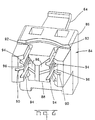
- the electrical connector 12 according to the present invention is shown mounted within the box 22.
- the box 22 includes a mounting wall 52 which is engaged by the latch 20 for retaining the connector 12 therein.
- the connector box 22 is conductive, either by having been formed from a conductive material or a metallized plastic, and the connector 12 is also advantageously formed of conductive material, such as metallized plastic, by placing the connector 12 within the box 22, the connector 12 will be electrically commoned thereto. This will have further advantageous effects.
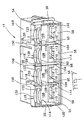
- the electrical connector 12 incorporates a main housing 14.
- the main housing 14 has a mating side 54 which in this example includes the card receiving slot 16 ( Figure 1). It is important to note that while the present invention can be advantageously used in a card-edge connector style, that the invention should not be limited.
- the main housing 14 also includes an open cable side 56 that is divided into a plurality of compartments 58 by partitions 60.
- the main housing 14 will be formed from a conductive material or metallized plastic.
- a plurality of contact carrying modules 62 are constructed to be received within compartments 58.
- the contact carrying modules 62 include opposing latches 64 so that they can be snapped in place within the main housing 14.
- the contact carrying module 62 is advantageously formed of insulative material although selective metallization could be used if desired.
- Each contact carrying module 62 includes two contacts 66 that are best seen and described in Figures 4 and 5. These contacts 66 include a mating end and a wire termination end 70.
- the connector 12 further includes a rear cover 18 that is fittable to the main housing 14 by a pair of latch arms 72 designed to engage corresponding catches 74 upon the main housing 14.
- the cover 18 further includes multiple U-shaped cable tabs 76. It is also envisioned that tabs 76 may be omitted.
- the rear cover 18 will also be manufactured from a conductive material or advantageously a metallized plastic.
- the contact 66 includes a mating end 68 that, in this embodiment, is a resilient tongue for engaging the conductive pads 38 of the card edge 36. Various configurations of this mating end 68 may be realized depending on the interface desired.
- the contact 66 further includes a cable termination end 70 that is formed as an insulation displacement contact (IDC).
- the IDC includes a wire receiving slot 78 for receiving an insulated wire and making connection thereto, as is well known in the industry.
- the wire termination end 70 could take on various other configurations, such as a crimp connection or a solder termination.
- a body section 80 is located between the mating end 68 and the wire termination end 70.
- the body portion 80 includes a retention lance 82 for incorporating the contact 66 into the contact carrying module 62.
- Various materials may be used for the contact 66 as desired and it may be advantageous to include a precious metal contact patch 84 for engaging the conductive pads 38 of the card edge 36.
- guide slots 94 that extend into the module 84 basically parallel to the contact receiving passageways 90. These guide slots 94, along with large chamfers 96 on both sides of the wire receiving slots 92, are useful for stabilizing a wire termination tool (not shown) that would be used to stuff the insulated wires into the IDC contact slot 70 of the contact 66 in a manner well known in industry.
- the open cable side 56 of the main housing 14 is shell-like and defined by a lower wall 98, opposing side walls 100, 102 and upper wall 103.
- This shell-like open cable side 56 is further divided into a row of compartments 58 by partitions 60 that extend between the lower wall 98 and the upper wall 103.
- the partitions 60 are formed as tongues having a chamfered surface 104 extending on a side thereof to an end 106 of the tongue 60.
- the end 106 of tongue 60 is slightly recessed from the open cable side 56 of the connector 14.
- Each compartment 58 further includes a table 108 having an inverted, U-shaped, end 110 defining a passageway 112 thereunder and a passageway 114 thereover.
- the passageway 114 extends through the housing 14 to the mating side 54 while the passageway 112 exposes a latch 116 for retaining the contact carrying module 62.
- the table 108 is used to position the contact module 62 within the main housing 14.
- the end cover 18 that is constructed to close the open cable side 56 of the main housing 14 will be described in greater detail.
- the end cover 18 includes latches 72 to engage the catches 30 of the main housing in order to fix the cover 18 to the main housing 14.
- the cover 18 includes a body portion 124 having a rearward side 126 and a connector side 128. An interior surface 130 of the rearward side 126 faces the connector side 128.
- a trough-like structure is formed.
- the trough-like structure is further divided into compartments 58A by second partitions 60A that correspond to the partitions 60 of the main housing 14, as will be described below with reference to Figures 11 and 12.
- the second partition 60A also include chamfers 104A that extend along sides of the partition 60A to ends 142. It is important to note that at least a portion of the chamfer 104A of the partition 60A extends beyond the connector surface 128 in order to provide the ends 142 of the partition 60 with some flexibility. In this particular embodiment, the second partition 60A itself extends a small distance 144 beyond the connector edge 128. Further, the end 142 of the partitions extends upwards to a ledge 146 such that the second partitions 60A would be received between the lower wall 98 and the upper wall 103 of the main housing 14 when the cover 18 is fitted thereto.
- the cover 18 would be manufactured from a conductive material or a metallized plastic mold.
- a portion 148 of the partition 60A extends above the ledge 146 to be received within slots 150 formed in the upper wall 103 of the main housing 14 that correspond to the partition 60 therein.
- a plurality of U-shaped tabs 76 located along the upper wall 140 of the cover 18 are a plurality of U-shaped tabs 76 constructed to be received within the troughs 122 of the main housing 14. These legs of the U-shaped tabs 76 may take on various lengths as desired and provide some strain relief for the twisted-pair wire 6 and discontinuity in any pathway. As mentioned above, these tabs 76 are optional.
- a second saddle portion 152 At the base of the U-shaped tab 76 is a second saddle portion 152 that will be disposed opposite the first saddle portion 118 in the main housing 14.
- the electrical connector 12 is shown in assembled form.
- the contact carrying module 62 with the contact 66 is fitted to the housing 14 by the latch members 64 engaging corresponding latches 116 formed in the main housing 14.
- the contact 66 extends through the contact carrying passageway 90 such that the mating end 68 is disposed in the card edge receiving slot 16 on the mating end 54 of the main housing 14.
- the contact 66 is retained therein by the locking lance 82 that is received in a recess 156 of the body 84 in order to further retain the contact 66.
- a staking operation can be performed that utilizes the recess 158 above the contact lance 82 prior to assembling of the module 62 with the main housing 14 to further assure contact retention.
- the main housing has been assembled to the extent shown in Figure 9.
- a wire exit 160 is defined by the two saddle portions 120, 152 of the main housing 14 and cover 18 respectively for each of the compartments 58.
- This wire exit 160 is configured to be slightly smaller than that of the wires exiting such that an interference will exist. This interference is advantageously taken advantage of by allowing the shielding 10 that surrounds the wires 8 to extend into the compartment and be terminated only slightly above the rear IDC portion 88 of the contact module 62 when the various conductors 6 are being terminated.
- what is realized from the present invention is a structure that continues the shielding 10 provided to the twisted pair of wires 8 to a compartment 58 within a connector 12 such that a fully shielded twisted-pair interconnection is provided, thereby greatly reducing the effect of cross-talk from adjacent signal conductors 6 and any spurious electro-magnetic fields.
Abstract
Description
- The present invention relates generally to electrical connectors and in particular to high transmission speed communication connectors.
- It is well known to transmit data over twisted-pair cabling for communication signal transmissions. A particular application where this cabling finds wide-spread use is in building wiring. In order to provide the flexibility necessary to utilize various pieces of equipment, which may have different interface requirements, it is desirable to have a flexible interconnect to the building wiring, as opposed to attempting to hard wire the equipment into the building wiring or to provide dedicated plugs for one particular interface requirements.
- One particularly advantageous flexible interconnect system is set out in EP 274 487. In this system, the building wiring is terminated in an edge-card connector. The edge-card connector is then mounted in a wall box. An interface insert that includes a common printed circuit board (PCB) with a standardized edge-card interface corresponding to the edge-card connector is provided. This insert further includes a communications connector mounted thereupon that is set in a mounting bezel so that as the insert is plugged into the edge-card, the bezel is received in the box. Depending upon the interface required, an insert with a different connector is incorporated onto the PCB and by exchanging the inserts, access to the building wiring is provided for various equipment interfaces. This provides the flexibility necessary to accommodate the many different types of equipment that are used within buildings today.
- Since this particularly flexible interconnection system has been introduced, the signal transmission speeds of copper-based communication systems have risen dramatically. As the signal transmission speeds have increased, so has the susceptibility of the signals being carried by the system to degradation from such things as the electro-magnetic interference from other electrical devices or cabling within the building and even adjacent signal line cross-talk.
- In order to accommodate the new signal transmission speeds, improved twisted-pair cabling has been developed. This cabling is known as foil shielded twisted-pair, screened foil shielded twisted-pair and pair in metal foil twisted-pair. These various shielding or screening techniques are used in order to try to prevent any outside influences from effecting the signal being transmitted along the cable and/or a particular twisted-pair. It is not uncommon, over the life of the building, for the internal wiring to be upgraded.
- In addition, improvements have been made to other parts of the system. For example, in EP 525 703 proposals to improve on an insert are set out. In addition, there has been much study relating to improving basic data connectors, such as the common modular jack receptacle. An example of this improvement is set out in US 5,186,647. Finally, it has been known to utilize metallized plastic boxes from US 5,484 308 or metal boxes for housing the cable termination and the edge-card connector. It is further known to electrically close the box by metallizing at least one side of the plastic adapter that fits around the connector mounted upon the PCB so that the interface with the building wiring is generally protected from the outside.
- However, signal speeds have continued to increase and further improvement on the existing system has brought the requirement to provide an improved edge-card connector. This improved edge-card connector should retain the desirable flexibility of the existing system and work with the already improved components thereof. Additionally, it is desirable that the improved edge-card connector would have backward compatibility so that it could be installed within existing systems. These goals have been met by the present invention, which while particularly attractive in an edge-card form, may be useful with other interfaces and outside of building wiring systems.
- The present invention addresses the aforementioned objects by providing a high frequency connector with: a main housing having an open mounting side, a cable side and a partition at the cable side defining two compartments where each compartment is in communication with the mounting side and the cable side; a plurality of contacts, where a pair of contacts are positioned in the compartments such that the contacts are exposed for mating with a complementary electrical interface on the mating side and wires of a cable on the cable side; and a rear cover that is fittable to the main housing on the cable side in order to close the open cable side and cover the exposed contacts therein where the cover further includes a second partition configured to mechanically and electrically engage the partition of the main housing where the two partitions are conductive and act as a shield between the two compartments.
- It is advantageous that this connector can be configured as an edge-card connector.
- It is further advantageous that the main housing and the cover can be conductive or metallized plastic to provide complete shielding of the interconnections within the connector and in particular individually shield the compartments.
- It is yet further advantageous that the compartments can be provided with a wire exit having a metallized saddle where any foil or screening about a twisted wire pair would sit such that shielding continuity would exist between the cable and the screening at a given compartment.
- It is still further advantageous that the partitions are formed with tongues having chamfered surfaces thereupon that abut with one another along the chamfers to assure shielding continuity between the compartments.
- An exemplary embodiment of the present invention will be described below with reference to the following figures, wherein:
- Figure 1 is an exploded perspective view of a building interface system utilizing a connector according to present invention;
- Figure 2 is a partially assembled view of Figure 1;
- Figure 3 is a partially exploded perspective view of the electrical connector utilized in the system of Figure 1 incorporating the present invention;
- Figure 4 is a top view of a contact of the connector of Figure 3;
- Figure 5 is a side view of the contact of Figure 4;
- Figure 6 is a rear perspective view of the contact carrying module used in the connector of Figure 3;
- Figure 7 is a rear perspective view of a main housing of the connector of Figure 3;
- Figure 8 is an interior perspective view of a cover of the connector of Figure 3;
- Figure 9 is a further assembled view of the electrical connector of Figure 3 shown ready for termination of the wires of a building cable;
- Figure 10 is a side sectional view of an assembled view of the connector of Figure 3;
- Figure 11 is a upper partial section view of the assembled connector of Figure 3; and
- Figure 12 is a detailed view taken from Figure 11 at detail A.
-
- With reference first to Figure 1, a building wiring system interface utilizing the present invention is shown generally at 2. This building wiring system consists of a
cable 4 havingmultiple signal conductors 6 in the form oftwisted wires 8 that are surrounded byindividual shielding 10, which could take on the form of a foil. Theconductors 6 are terminated by anelectrical connector 12 incorporating the present invention. Theelectrical connector 12 includes amain housing 14 having an edge-card receivingslot 16 and arear cover 18. Theconnector 12 further includes alatch 20 for retaining theconnector 12 in anaccess box 22. While theconnector 12 utilizes an integrally moldedlatch 20, for snapping theconnector 12 into thebox 22, other mounting techniques may be used, such as a screw or other fastener. Thebox 22 is a rectangular shell having aforward opening 24, arear end 26 and acable exit 28. The forward end includeslatches 30 for retaining aninsert 32 therein. Theinsert 32 includes a PCB 34 having arear end 36 formed as a card edge with multiple conductors 38 thereupon. Aconnector 40 is incorporated onto the PCB 34. In particular, thisconnector 40 is a modular jack receptacle and provides aninterface 42 for receiving a modular jack plug (not shown). Theinterface 42 is surrounded by abezel 44 that includeslatch arms 46 to engagelatches 30 inbox 22 when theinsert 32 is placed within thebox 22. - A
rear cover 48 is provided to close therear end 26 of thebox 22 once theconnector 12 is mounted therein. Therear cover 48 includes atab 50 that is received within theslot 28 ofbox 22 when thecover 48 is affixed thereto. Thetab 50, in cooperation with the edges of theslot 28, engages thecable 4 to provide strain relief and possibly grounding of any general shielding of thecable 4 to thebox 22. - With reference now to Figure 2, the
electrical connector 12 according to the present invention is shown mounted within thebox 22. Thebox 22 includes amounting wall 52 which is engaged by thelatch 20 for retaining theconnector 12 therein. If theconnector box 22 is conductive, either by having been formed from a conductive material or a metallized plastic, and theconnector 12 is also advantageously formed of conductive material, such as metallized plastic, by placing theconnector 12 within thebox 22, theconnector 12 will be electrically commoned thereto. This will have further advantageous effects. - With reference now to Figure 3, the
electrical connector 12 will now be described in greater detail. Theelectrical connector 12 incorporates amain housing 14. Themain housing 14 has amating side 54 which in this example includes the card receiving slot 16 (Figure 1). It is important to note that while the present invention can be advantageously used in a card-edge connector style, that the invention should not be limited. Themain housing 14 also includes anopen cable side 56 that is divided into a plurality ofcompartments 58 bypartitions 60. Advantageously, themain housing 14 will be formed from a conductive material or metallized plastic. - A plurality of
contact carrying modules 62 are constructed to be received withincompartments 58. Thecontact carrying modules 62 include opposinglatches 64 so that they can be snapped in place within themain housing 14. Thecontact carrying module 62 is advantageously formed of insulative material although selective metallization could be used if desired. Eachcontact carrying module 62 includes twocontacts 66 that are best seen and described in Figures 4 and 5. Thesecontacts 66 include a mating end and awire termination end 70. - The
connector 12 further includes arear cover 18 that is fittable to themain housing 14 by a pair oflatch arms 72 designed to engage correspondingcatches 74 upon themain housing 14. Thecover 18 further includes multipleU-shaped cable tabs 76. It is also envisioned thattabs 76 may be omitted. Therear cover 18 will also be manufactured from a conductive material or advantageously a metallized plastic. - With reference now to Figures 4 and 5, the
contact 66 will be described in greater detail. Thecontact 66 includes amating end 68 that, in this embodiment, is a resilient tongue for engaging the conductive pads 38 of thecard edge 36. Various configurations of thismating end 68 may be realized depending on the interface desired. Thecontact 66 further includes acable termination end 70 that is formed as an insulation displacement contact (IDC). The IDC includes awire receiving slot 78 for receiving an insulated wire and making connection thereto, as is well known in the industry. Thewire termination end 70 could take on various other configurations, such as a crimp connection or a solder termination. Abody section 80 is located between themating end 68 and thewire termination end 70. Thebody portion 80 includes aretention lance 82 for incorporating thecontact 66 into thecontact carrying module 62. Various materials may be used for thecontact 66 as desired and it may be advantageous to include a preciousmetal contact patch 84 for engaging the conductive pads 38 of thecard edge 36. - With reference now to Figure 6, a
body 84 that substantially makes up thecontact carrying module 66 will be described in detail. Thebody 84 carries the twolatches 64 extending from afront surface 86 thereof. Thelatches 64 retain acontact carrying module 62 within themain housing 14 in a manner best seen in Figure 10. Thebody 84 includes arear IDC portion 88 having a pair ofcontact passageways 90 that extend through thebody 84 and open at thefront surface 86 so that acontact 66 may be disposed therein (best seen in Figure 10). Awire receiving slot 92 extends across theIDC termination portion 88 and the associatedcontact passageways 90 and is constructed for receiving theindividual wires 8 of the twisted-pair conductors 6 therein. Additionally, on either side of thecontact carrying passageway 90 areguide slots 94 that extend into themodule 84 basically parallel to thecontact receiving passageways 90. These guideslots 94, along withlarge chamfers 96 on both sides of thewire receiving slots 92, are useful for stabilizing a wire termination tool (not shown) that would be used to stuff the insulated wires into theIDC contact slot 70 of thecontact 66 in a manner well known in industry. - With reference now to Figure 7, the
main housing 14 will be described in greater detail. Theopen cable side 56 of themain housing 14 is shell-like and defined by alower wall 98, opposingside walls upper wall 103. This shell-likeopen cable side 56 is further divided into a row ofcompartments 58 bypartitions 60 that extend between thelower wall 98 and theupper wall 103. Advantageously, in this embodiment, thepartitions 60 are formed as tongues having a chamferedsurface 104 extending on a side thereof to anend 106 of thetongue 60. Theend 106 oftongue 60 is slightly recessed from theopen cable side 56 of theconnector 14. - Each
compartment 58 further includes a table 108 having an inverted, U-shaped, end 110 defining apassageway 112 thereunder and apassageway 114 thereover. Thepassageway 114 extends through thehousing 14 to themating side 54 while thepassageway 112 exposes alatch 116 for retaining thecontact carrying module 62. The table 108 is used to position thecontact module 62 within themain housing 14. - The
upper wall 103 is considerably thicker than thelower wall 98 or theside walls upper wall 103 carries at least a first portion of awire exit saddle 118. The first portion of thiswire exit saddle 118 includes a pair of scalloped saddle surfaces 120 that are separated by atab receiving trough 122 that extends into thewall 103 for receiving theU-shaped tabs 76 of thecover 18, as will be described below. As mentioned above, themain housing 14 would either be manufactured from a conductive material or molded from plastic and metallized such that themain housing 14 would provide shielding or anything received therein. - With reference now to Figure 8, the
end cover 18 that is constructed to close theopen cable side 56 of themain housing 14 will be described in greater detail. Theend cover 18 includeslatches 72 to engage thecatches 30 of the main housing in order to fix thecover 18 to themain housing 14. Thecover 18 includes abody portion 124 having arearward side 126 and aconnector side 128. Aninterior surface 130 of therearward side 126 faces theconnector side 128. Combined withside walls lower wall 136 andupper wall 140, a trough-like structure is formed. The trough-like structure is further divided into compartments 58A by second partitions 60A that correspond to thepartitions 60 of themain housing 14, as will be described below with reference to Figures 11 and 12. The second partition 60A also include chamfers 104A that extend along sides of the partition 60A to ends 142. It is important to note that at least a portion of the chamfer 104A of the partition 60A extends beyond theconnector surface 128 in order to provide theends 142 of thepartition 60 with some flexibility. In this particular embodiment, the second partition 60A itself extends asmall distance 144 beyond theconnector edge 128. Further, theend 142 of the partitions extends upwards to aledge 146 such that the second partitions 60A would be received between thelower wall 98 and theupper wall 103 of themain housing 14 when thecover 18 is fitted thereto. Advantageously, thecover 18 would be manufactured from a conductive material or a metallized plastic mold. Aportion 148 of the partition 60A extends above theledge 146 to be received withinslots 150 formed in theupper wall 103 of themain housing 14 that correspond to thepartition 60 therein. In addition, located along theupper wall 140 of thecover 18 are a plurality ofU-shaped tabs 76 constructed to be received within thetroughs 122 of themain housing 14. These legs of theU-shaped tabs 76 may take on various lengths as desired and provide some strain relief for the twisted-pair wire 6 and discontinuity in any pathway. As mentioned above, thesetabs 76 are optional. At the base of theU-shaped tab 76 is asecond saddle portion 152 that will be disposed opposite thefirst saddle portion 118 in themain housing 14. - With reference now to Figure 9, the
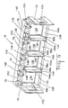
electrical connector 12 is shown in partially assembled form. Thecontact carrying modules 62, with thecontacts 66 therein, are shown received within themain housing 14. Thecover 18 is positioned to be mounted upon themain housing 14. As can be seen, the partition 60A will be received between adjacentcontact carrying modules 62 and theupper portions 148 of the partition 60A will be received in theslots 150. Additionally, if desired to improve the flexibility of thecover 18,reliefs 154 may be provided in therear surface 126. - With reference now to Figure 10, the
electrical connector 12 is shown in assembled form. Thecontact carrying module 62 with thecontact 66 is fitted to thehousing 14 by thelatch members 64 engagingcorresponding latches 116 formed in themain housing 14. Thecontact 66 extends through thecontact carrying passageway 90 such that themating end 68 is disposed in the cardedge receiving slot 16 on themating end 54 of themain housing 14. Thecontact 66 is retained therein by the lockinglance 82 that is received in arecess 156 of thebody 84 in order to further retain thecontact 66. A staking operation can be performed that utilizes therecess 158 above thecontact lance 82 prior to assembling of themodule 62 with themain housing 14 to further assure contact retention. At this point, the main housing has been assembled to the extent shown in Figure 9. - With the
cover 18 attached to themain housing 14 as shown in Figure 10, theopen cable side 56 of themain housing 14 has been closed. Awire exit 160 is defined by the twosaddle portions main housing 14 and cover 18 respectively for each of thecompartments 58. Thiswire exit 160 is configured to be slightly smaller than that of the wires exiting such that an interference will exist. This interference is advantageously taken advantage of by allowing the shielding 10 that surrounds thewires 8 to extend into the compartment and be terminated only slightly above therear IDC portion 88 of thecontact module 62 when thevarious conductors 6 are being terminated. Once thecover 18 is attached to themain housing 14, it is easily recognized that thesaddle portions main housing 14 and thecover 18 are manufactured from either conductive material or metallized plastic, the saddle surfaces 120, 152 are electrically commoned to the shielding 10. - Returning to Figure 1 and Figure 2, it can be seen that as a result of closing of the
rear cover 18 upon themain housing 14 with theconductors 6 extending therefrom, the shielding 10 of the individual conductors is slightly compressed in theregion 161 indicating engagement with thehousing 14 andcover 18. - With reference now to Figures 11 and 12, in addition to providing for the commoning of the conductive
main housing 14 andrear cover 18 to the shielding 10 of theindividual conductors 6 by way of thesaddle portions adjacent compartments 58 are completely isolated from one another. This is reliably achieved by thefirst partitions 60 of themain housing 14 and the second partition 60A of thecover 18 being provided withrespective chamfers 104, 104A and configured such that the respective ends 106, 142 also overlap and result in aslight interference 162 within thespace 164 betweenadjacent modules 84 contained within theirrespective compartments 58. As can be imagined, thisspace 164 and the associated partition walls are extremely thin and, hence, some flexibility of thepartitions 60, 60A is realized. Furthermore, it is this space requirement that prevents easily manufacturing these partitions as a single piece extending outward from either thecover 18 or thehousing 14 exclusively. As each of thepartitions 60, 60A are conductive, a shielding partition is formed betweenadjacent compartments 58. - Advantageously then, what is realized from the present invention is a structure that continues the shielding 10 provided to the twisted pair of
wires 8 to acompartment 58 within aconnector 12 such that a fully shielded twisted-pair interconnection is provided, thereby greatly reducing the effect of cross-talk fromadjacent signal conductors 6 and any spurious electro-magnetic fields.
Claims (6)
- A high frequency connector; comprising:a main housing having an open mounting side, a cable side and a partition at the cable side defining two compartments where each compartment is in communication with the mounting side and the cable side;a plurality of contacts, where a pair of contacts are positioned in the compartments such that the contacts are exposed from mating with a complementary electrical interface on the mating side and wires of a cable on the cable side; anda rear cover that is fittable to the main housing on the cable side in order to close the open cable side and cover the exposed contacts therein where the cover further includes a second partition configured to mechanically and electrically engage the partition of the main housing where the two partitions are conductive and act as a shield between the two compartments.
- The high frequency connector of claim 1, wherein the connector includes a conductive saddle for electrically engaging a conductive shield about the wires of the cable.
- The high frequency connector of claim 2, wherein the connector includes conductive saddles at each compartment.
- The high frequency connector of claim 3, wherein a saddle portion is formed on each of the main housing and the rear cover to capture the conductive shield therebetween.
- The high frequency connector of claim 1, wherein one of the partition or second partition includes a tapered section to engage the other.
- The high frequency connector of claim 5, wherein both partitions include complementary tapered sections.
Priority Applications (1)
| Application Number | Priority Date | Filing Date | Title |
|---|---|---|---|
| EP20010104117 EP1128488B1 (en) | 2000-02-21 | 2001-02-21 | Electrical connector for high speed signal transmission |
Applications Claiming Priority (3)
| Application Number | Priority Date | Filing Date | Title |
|---|---|---|---|
| EP00103625 | 2000-02-21 | ||
| EP00103625 | 2000-02-21 | ||
| EP20010104117 EP1128488B1 (en) | 2000-02-21 | 2001-02-21 | Electrical connector for high speed signal transmission |
Publications (3)
| Publication Number | Publication Date |
|---|---|
| EP1128488A2 true EP1128488A2 (en) | 2001-08-29 |
| EP1128488A3 EP1128488A3 (en) | 2013-07-31 |
| EP1128488B1 EP1128488B1 (en) | 2015-02-11 |
Family
ID=26070576
Family Applications (1)
| Application Number | Title | Priority Date | Filing Date |
|---|---|---|---|
| EP20010104117 Expired - Lifetime EP1128488B1 (en) | 2000-02-21 | 2001-02-21 | Electrical connector for high speed signal transmission |
Country Status (1)
| Country | Link |
|---|---|
| EP (1) | EP1128488B1 (en) |
Cited By (6)
| Publication number | Priority date | Publication date | Assignee | Title |
|---|---|---|---|---|
| EP1531523A2 (en) * | 2003-11-13 | 2005-05-18 | Tyco Electronics AMP GmbH | Lead connector for circuit board |
| WO2005124940A2 (en) * | 2004-06-10 | 2005-12-29 | Commscope Solutions Properties, Llc | Shielded jack assemblies and methods for forming a cable termination |
| US7033219B2 (en) | 2004-06-10 | 2006-04-25 | Commscope Solutions Properties, Llc | Modular plug assemblies, terminated cable assemblies and methods for forming the same |
| WO2006065972A1 (en) * | 2004-12-17 | 2006-06-22 | Panduit Corp. | Systems for reducing crosstalk between communications connectors |
| CN100539323C (en) * | 2004-06-10 | 2009-09-09 | 北卡罗来纳科姆斯科普公司 | Jack assemblies and the method that is used to make this jack assemblies |
| WO2011003914A1 (en) * | 2009-07-08 | 2011-01-13 | Tyco Electronics Amp Gmbh | Electrical plug connector having a one-piece connector housing and assembly method |
Citations (4)
| Publication number | Priority date | Publication date | Assignee | Title |
|---|---|---|---|---|
| EP0274487A1 (en) | 1986-06-13 | 1988-07-20 | Amp Inc | Local area network interface. |
| EP0525703A1 (en) | 1991-08-01 | 1993-02-03 | Siemens Aktiengesellschaft | Connector for local networks |
| US5186647A (en) | 1992-02-24 | 1993-02-16 | At&T Bell Laboratories | High frequency electrical connector |
| US5484308A (en) | 1993-04-29 | 1996-01-16 | The Whitaker Corporation | Data communications outlet kit |
Family Cites Families (2)
| Publication number | Priority date | Publication date | Assignee | Title |
|---|---|---|---|---|
| US5605469A (en) * | 1995-01-05 | 1997-02-25 | Thomas & Betts Corporation | Electrical connector having an improved conductor holding block and conductor shield |
| ES2135199T3 (en) * | 1996-05-23 | 1999-10-16 | Bks Kabel Service Ag | MULTIPOLAR CONNECTOR SYSTEM THAT HAS AT LEAST ONE CONNECTOR FOR THE ELECTRICAL AND MECHANICAL CONNECTION OF ELECTRICAL CONDUCTORS. |
-
2001
- 2001-02-21 EP EP20010104117 patent/EP1128488B1/en not_active Expired - Lifetime
Patent Citations (4)
| Publication number | Priority date | Publication date | Assignee | Title |
|---|---|---|---|---|
| EP0274487A1 (en) | 1986-06-13 | 1988-07-20 | Amp Inc | Local area network interface. |
| EP0525703A1 (en) | 1991-08-01 | 1993-02-03 | Siemens Aktiengesellschaft | Connector for local networks |
| US5186647A (en) | 1992-02-24 | 1993-02-16 | At&T Bell Laboratories | High frequency electrical connector |
| US5484308A (en) | 1993-04-29 | 1996-01-16 | The Whitaker Corporation | Data communications outlet kit |
Cited By (14)
| Publication number | Priority date | Publication date | Assignee | Title |
|---|---|---|---|---|
| EP1531523A2 (en) * | 2003-11-13 | 2005-05-18 | Tyco Electronics AMP GmbH | Lead connector for circuit board |
| US7134904B2 (en) | 2003-11-13 | 2006-11-14 | Tyco Electronics Amp Gmbh | Terminal unit for putting a lead into contact with a printed circuit board |
| EP1531523A3 (en) * | 2003-11-13 | 2006-03-01 | Tyco Electronics AMP GmbH | Lead connector for circuit board |
| US7083472B2 (en) | 2004-06-10 | 2006-08-01 | Commscope Solutions Properties, Llc | Shielded jack assemblies and methods for forming a cable termination |
| WO2005124940A3 (en) * | 2004-06-10 | 2006-05-04 | Commscope Solutions Properties | Shielded jack assemblies and methods for forming a cable termination |
| US7033219B2 (en) | 2004-06-10 | 2006-04-25 | Commscope Solutions Properties, Llc | Modular plug assemblies, terminated cable assemblies and methods for forming the same |
| WO2005124940A2 (en) * | 2004-06-10 | 2005-12-29 | Commscope Solutions Properties, Llc | Shielded jack assemblies and methods for forming a cable termination |
| US7249974B2 (en) | 2004-06-10 | 2007-07-31 | Commscope, Inc. Of North Carolina | Shielded jack assemblies and methods for forming a cable termination |
| US7510439B2 (en) | 2004-06-10 | 2009-03-31 | Commscope, Inc. Of North Carolina | Shielded jack assemblies and methods for forming a cable termination |
| CN100539323C (en) * | 2004-06-10 | 2009-09-09 | 北卡罗来纳科姆斯科普公司 | Jack assemblies and the method that is used to make this jack assemblies |
| AU2005255867B2 (en) * | 2004-06-10 | 2010-05-20 | Commscope, Inc. Of North Carolina | Shielded jack assemblies and methods for forming a cable termination |
| AU2005255867C1 (en) * | 2004-06-10 | 2010-10-14 | Commscope, Inc. Of North Carolina | Shielded jack assemblies and methods for forming a cable termination |
| WO2006065972A1 (en) * | 2004-12-17 | 2006-06-22 | Panduit Corp. | Systems for reducing crosstalk between communications connectors |
| WO2011003914A1 (en) * | 2009-07-08 | 2011-01-13 | Tyco Electronics Amp Gmbh | Electrical plug connector having a one-piece connector housing and assembly method |
Also Published As
| Publication number | Publication date |
|---|---|
| EP1128488A3 (en) | 2013-07-31 |
| EP1128488B1 (en) | 2015-02-11 |
Similar Documents
| Publication | Publication Date | Title |
|---|---|---|
| US6394844B1 (en) | Electrical connector for high speed signal transmission | |
| USRE38519E1 (en) | Low crosstalk modular communication connector | |
| EP0992084B1 (en) | Shielded cable connector | |
| EP0460976B1 (en) | Connectors with ground structure | |
| EP0080772B1 (en) | Jack and plug electrical assembly | |
| EP0658953B1 (en) | Multi-port modular jack assembly | |
| US6705902B1 (en) | Connector assembly having contacts with uniform electrical property of resistance | |
| EP1356549B1 (en) | Connector interface and retention system for high-density connector | |
| US6478610B1 (en) | Electrical connector assembly | |
| EP1923970A2 (en) | Low crosstalk modular communication connector | |
| EP1450442A2 (en) | Connector apparatus | |
| EP0460975A1 (en) | Connectors with ground structure | |
| US6582255B2 (en) | High-density plug connector for twisted pair cable | |
| US11239617B2 (en) | Cable receptacle connector | |
| EP0614248B1 (en) | Local area network interface | |
| US5151036A (en) | Connectors with ground structure | |
| US5141453A (en) | Connectors with ground structure | |
| US5261829A (en) | Connectors with ground structure | |
| US6184460B1 (en) | Modular box shield for forming a coaxial header | |
| GB2428337A (en) | Enhanced jack with plug engaging printed circuit board | |
| US6887094B2 (en) | Shielded connection arrangement for data transfer | |
| EP1128488B1 (en) | Electrical connector for high speed signal transmission | |
| US6375506B1 (en) | High-density high-speed input/output connector | |
| EP1166400A2 (en) | Electrical connector | |
| US20220384984A1 (en) | High density coupling panel |
Legal Events
| Date | Code | Title | Description |
|---|---|---|---|
| PUAI | Public reference made under article 153(3) epc to a published international application that has entered the european phase |
Free format text: ORIGINAL CODE: 0009012 |
|
| AK | Designated contracting states |
Kind code of ref document: A2 Designated state(s): AT BE CH CY DE DK ES FI FR GB GR IE IT LI LU MC NL PT SE TR |
|
| AX | Request for extension of the european patent |
Free format text: AL;LT;LV;MK;RO;SI |
|
| PUAL | Search report despatched |
Free format text: ORIGINAL CODE: 0009013 |
|
| AK | Designated contracting states |
Kind code of ref document: A3 Designated state(s): AT BE CH CY DE DK ES FI FR GB GR IE IT LI LU MC NL PT SE TR |
|
| AX | Request for extension of the european patent |
Extension state: AL LT LV MK RO SI |
|
| RIC1 | Information provided on ipc code assigned before grant |
Ipc: H01R 13/658 20110101AFI20130627BHEP |
|
| RAP1 | Party data changed (applicant data changed or rights of an application transferred) |
Owner name: TYCO ELECTRONICS AMP ESPANA S.A. |
|
| 17P | Request for examination filed |
Effective date: 20140121 |
|
| RBV | Designated contracting states (corrected) |
Designated state(s): AT BE CH CY DE DK ES FI FR GB GR IE IT LI LU MC NL PT SE TR |
|
| AKX | Designation fees paid |
Designated state(s): AT BE CH CY DE DK ES FI FR GB GR IE IT LI LU MC NL PT SE TR |
|
| 17Q | First examination report despatched |
Effective date: 20140319 |
|
| GRAP | Despatch of communication of intention to grant a patent |
Free format text: ORIGINAL CODE: EPIDOSNIGR1 |
|
| INTG | Intention to grant announced |
Effective date: 20140819 |
|
| GRAS | Grant fee paid |
Free format text: ORIGINAL CODE: EPIDOSNIGR3 |
|
| GRAA | (expected) grant |
Free format text: ORIGINAL CODE: 0009210 |
|
| AK | Designated contracting states |
Kind code of ref document: B1 Designated state(s): AT BE CH CY DE DK ES FI FR GB GR IE IT LI LU MC NL PT SE TR |
|
| REG | Reference to a national code |
Ref country code: GB Ref legal event code: FG4D |
|
| REG | Reference to a national code |
Ref country code: CH Ref legal event code: EP |
|
| REG | Reference to a national code |
Ref country code: IE Ref legal event code: FG4D |
|
| REG | Reference to a national code |
Ref country code: CH Ref legal event code: NV Representative=s name: MURGITROYD AND COMPANY, CH |
|
| REG | Reference to a national code |
Ref country code: AT Ref legal event code: REF Ref document number: 710177 Country of ref document: AT Kind code of ref document: T Effective date: 20150315 |
|
| REG | Reference to a national code |
Ref country code: DE Ref legal event code: R096 Ref document number: 60149230 Country of ref document: DE Effective date: 20150326 |
|
| REG | Reference to a national code |
Ref country code: NL Ref legal event code: VDEP Effective date: 20150211 |
|
| PG25 | Lapsed in a contracting state [announced via postgrant information from national office to epo] |
Ref country code: BE Free format text: LAPSE BECAUSE OF NON-PAYMENT OF DUE FEES Effective date: 20150228 |
|
| PG25 | Lapsed in a contracting state [announced via postgrant information from national office to epo] |
Ref country code: SE Free format text: LAPSE BECAUSE OF FAILURE TO SUBMIT A TRANSLATION OF THE DESCRIPTION OR TO PAY THE FEE WITHIN THE PRESCRIBED TIME-LIMIT Effective date: 20150211 Ref country code: ES Free format text: LAPSE BECAUSE OF FAILURE TO SUBMIT A TRANSLATION OF THE DESCRIPTION OR TO PAY THE FEE WITHIN THE PRESCRIBED TIME-LIMIT Effective date: 20150211 Ref country code: FI Free format text: LAPSE BECAUSE OF FAILURE TO SUBMIT A TRANSLATION OF THE DESCRIPTION OR TO PAY THE FEE WITHIN THE PRESCRIBED TIME-LIMIT Effective date: 20150211 |
|
| PG25 | Lapsed in a contracting state [announced via postgrant information from national office to epo] |
Ref country code: GR Free format text: LAPSE BECAUSE OF FAILURE TO SUBMIT A TRANSLATION OF THE DESCRIPTION OR TO PAY THE FEE WITHIN THE PRESCRIBED TIME-LIMIT Effective date: 20150512 Ref country code: NL Free format text: LAPSE BECAUSE OF FAILURE TO SUBMIT A TRANSLATION OF THE DESCRIPTION OR TO PAY THE FEE WITHIN THE PRESCRIBED TIME-LIMIT Effective date: 20150211 |
|
| PG25 | Lapsed in a contracting state [announced via postgrant information from national office to epo] |
Ref country code: DK Free format text: LAPSE BECAUSE OF FAILURE TO SUBMIT A TRANSLATION OF THE DESCRIPTION OR TO PAY THE FEE WITHIN THE PRESCRIBED TIME-LIMIT Effective date: 20150211 |
|
| REG | Reference to a national code |
Ref country code: DE Ref legal event code: R097 Ref document number: 60149230 Country of ref document: DE |
|
| REG | Reference to a national code |
Ref country code: IE Ref legal event code: MM4A |
|
| PG25 | Lapsed in a contracting state [announced via postgrant information from national office to epo] |
Ref country code: MC Free format text: LAPSE BECAUSE OF FAILURE TO SUBMIT A TRANSLATION OF THE DESCRIPTION OR TO PAY THE FEE WITHIN THE PRESCRIBED TIME-LIMIT Effective date: 20150211 |
|
| PLBE | No opposition filed within time limit |
Free format text: ORIGINAL CODE: 0009261 |
|
| STAA | Information on the status of an ep patent application or granted ep patent |
Free format text: STATUS: NO OPPOSITION FILED WITHIN TIME LIMIT |
|
| PG25 | Lapsed in a contracting state [announced via postgrant information from national office to epo] |
Ref country code: IT Free format text: LAPSE BECAUSE OF FAILURE TO SUBMIT A TRANSLATION OF THE DESCRIPTION OR TO PAY THE FEE WITHIN THE PRESCRIBED TIME-LIMIT Effective date: 20150211 |
|
| 26N | No opposition filed |
Effective date: 20151112 |
|
| GBPC | Gb: european patent ceased through non-payment of renewal fee |
Effective date: 20150511 |
|
| PG25 | Lapsed in a contracting state [announced via postgrant information from national office to epo] |
Ref country code: IE Free format text: LAPSE BECAUSE OF NON-PAYMENT OF DUE FEES Effective date: 20150221 |
|
| REG | Reference to a national code |
Ref country code: FR Ref legal event code: PLFP Year of fee payment: 16 |
|
| REG | Reference to a national code |
Ref country code: AT Ref legal event code: UEP Ref document number: 710177 Country of ref document: AT Kind code of ref document: T Effective date: 20150211 |
|
| PG25 | Lapsed in a contracting state [announced via postgrant information from national office to epo] |
Ref country code: GB Free format text: LAPSE BECAUSE OF NON-PAYMENT OF DUE FEES Effective date: 20150511 |
|
| PG25 | Lapsed in a contracting state [announced via postgrant information from national office to epo] |
Ref country code: BE Free format text: LAPSE BECAUSE OF FAILURE TO SUBMIT A TRANSLATION OF THE DESCRIPTION OR TO PAY THE FEE WITHIN THE PRESCRIBED TIME-LIMIT Effective date: 20150211 |
|
| REG | Reference to a national code |
Ref country code: FR Ref legal event code: PLFP Year of fee payment: 17 |
|
| PG25 | Lapsed in a contracting state [announced via postgrant information from national office to epo] |
Ref country code: CY Free format text: LAPSE BECAUSE OF FAILURE TO SUBMIT A TRANSLATION OF THE DESCRIPTION OR TO PAY THE FEE WITHIN THE PRESCRIBED TIME-LIMIT Effective date: 20150211 |
|
| PG25 | Lapsed in a contracting state [announced via postgrant information from national office to epo] |
Ref country code: PT Free format text: LAPSE BECAUSE OF FAILURE TO SUBMIT A TRANSLATION OF THE DESCRIPTION OR TO PAY THE FEE WITHIN THE PRESCRIBED TIME-LIMIT Effective date: 20150611 |
|
| PG25 | Lapsed in a contracting state [announced via postgrant information from national office to epo] |
Ref country code: TR Free format text: LAPSE BECAUSE OF FAILURE TO SUBMIT A TRANSLATION OF THE DESCRIPTION OR TO PAY THE FEE WITHIN THE PRESCRIBED TIME-LIMIT Effective date: 20150211 |
|
| PG25 | Lapsed in a contracting state [announced via postgrant information from national office to epo] |
Ref country code: LU Free format text: LAPSE BECAUSE OF NON-PAYMENT OF DUE FEES Effective date: 20150221 |
|
| REG | Reference to a national code |
Ref country code: FR Ref legal event code: PLFP Year of fee payment: 18 |
|
| PGFP | Annual fee paid to national office [announced via postgrant information from national office to epo] |
Ref country code: DE Payment date: 20200227 Year of fee payment: 20 |
|
| PGFP | Annual fee paid to national office [announced via postgrant information from national office to epo] |
Ref country code: FR Payment date: 20200225 Year of fee payment: 20 |
|
| REG | Reference to a national code |
Ref country code: CH Ref legal event code: PL |
|
| REG | Reference to a national code |
Ref country code: AT Ref legal event code: MM01 Ref document number: 710177 Country of ref document: AT Kind code of ref document: T Effective date: 20200221 |
|
| PG25 | Lapsed in a contracting state [announced via postgrant information from national office to epo] |
Ref country code: CH Free format text: LAPSE BECAUSE OF NON-PAYMENT OF DUE FEES Effective date: 20200229 Ref country code: LI Free format text: LAPSE BECAUSE OF NON-PAYMENT OF DUE FEES Effective date: 20200229 Ref country code: AT Free format text: LAPSE BECAUSE OF NON-PAYMENT OF DUE FEES Effective date: 20200221 |
|
| REG | Reference to a national code |
Ref country code: DE Ref legal event code: R071 Ref document number: 60149230 Country of ref document: DE |